CHAPTER 10
![]()
Audio Circuits
We will explore two types of audio amplifiers—preamplifiers, commonly known as preamps, and power amplifiers.
The examples chosen will be from commercially manufactured designs. What’s different in this chapter is that in some cases, we will see associated circuits such as a power supply and a voltage regulator. Although integrated circuit (IC) amplifiers could have been chosen for this chapter, it would be good to know something more about amplifiers on the transistor level. This way you can use this knowledge to augment IC designs with discrete circuits.
NOTE: Audio signals are usually measured in RMS voltages. For a sine wave signal, the peak to peak voltage is 2.82 x RMS voltage. For example, a 1-volt RMS sine wave is 2.82 volts peak to peak. However, when you are measuring the audio signal on an oscilloscope, you will often measure the peak to peak amplitude instead of the RMS value.
Preamps and Power Amps
For transducers such as microphones and phonograph pickup cartridges that generate small amplitude signals in the 1 mV to 10 mV range, preamps are needed to provide large voltage gains for these devices. For example, a microphone preamp has a voltage gain of 30 to 1000.
A dynamic microphone needs a preamp gain of about 300 or 50 dB. There are higher output microphones such as electret types. These require power, and they generally have about 10 times more output signal than a dynamic microphone; so they only require gains of 30 or about 30 dB. Low-level microphone preamps have voltage gains from about 30 to 1000 (30 dB to 60 dB) with flat frequency response from 20 Hz to 20,000 Hz.
NOTE: Decibels or dB = 20 log10(|Vout/Vin|) where the voltage gain = |Vout/Vin|. For example if you have a 2 volt RMS input signal and the output is 10 volts RMS, then the gain = |10 volts RMS/2 volts RMS| = 5 and in decibels we have 20log10(5) dB = 14 dB since log10(5) = 0.7. Also log10(x) is commonly known as just log(x), where x is a non-negative number. For example, x ≥ 0.
Magnetic phonograph pick up cartridges (a.k.a., phono cartridges such as Shure M97xE or Audio Technica AT95E) for playing (LP) vinyl records generally require a gain of 50 to 100 at 1 kHz. The phono cartridge preamp requires a frequency equalization to provide flat frequency response from the vinyl record to the output of the preamp. That is, the vinyl recording is cut with a non-flat frequency response. This is done to maximize playing time by essentially attenuating low frequencies while boosting higher frequencies.
For higher (amplitude) level signals, we use line-level preamps that have a gain of 1 to about 10 or 0 dB to 20 dB. Line-level signals are in the order of 70 mV RMS to about 1 volt RMS. A typical portable digital audio device may output a maximum of about 1 volt RMS or about 2.82 volts peak to peak. Preamplifiers, whether low-level or line-level types, do not provide enough current output to drive a loudspeaker. However, some preamps can drive headphones.
The ultimate goal for the preamp is to provide enough signal level to a power amplifier. Typically, an audio power amplifier will be specified for an input voltage for full power output.
For example, many audio power amps have a gain of 26 dB or 20. If the amplifier is specified for 2 volts RMS input for full output into an 8Ω speaker load, then the power output will be output RMS voltage squared, divided by the load resistance. In this example, power output will then be P = [(2 volts RMS × 20)2/8 Ω]. Thus, P = [402/8] watts = [1600/8] watts, or P = 200 watts output into the 8Ω load.
For this chapter we will look into a Dynaco PAT-5 low-level preamp and two different power amplifiers from the Pioneer SX-626 and SX-636 stereo receivers.
First, we need to discuss differencing amplifiers and emitter follower amplifiers and how they will relate to preamps, power amps, or voltage regulators.
Now let’s look at some building blocks to preamp and power amps.
A Basic Difference Amplifier
In most modern amplifiers, negative feedback is used. This requires an inverting input terminal, and a non-inverting input terminal. For example, the voltage follower circuit using an op amp has the output terminal connected to the inverting input terminal while the input signal is applied to the non-inverting input terminal (e.g., Chapter 9, Figure 9-3).
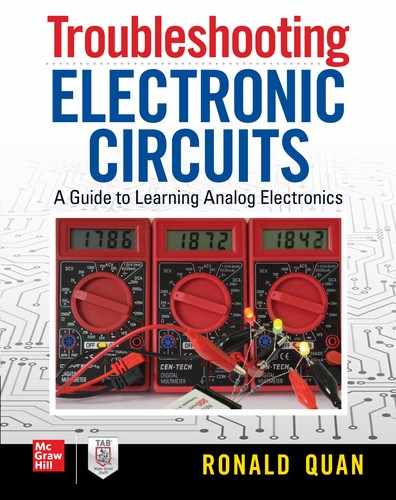
A difference amplifier can be made with a common emitter amplifier and a common base amplifier. What we want is for the difference amplifier to provide an output signal that somehow subtracts two input signals. First let’s take a look at each amplifier in Figure 10-1.
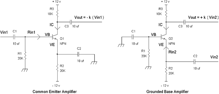
FIGURE 10.1 A common emitter amplifier with input signal Vin1 and a common base amplifier with a second input signal Vin2.
The common emitter amplifier in Figure 10-1 provides an inverting gain referenced to input signal Vin1. In both figures, VE = emitter voltage, VB = base voltage, IC = collector current, Rin1 = input AC resistance Q1’s base, and Rin2 = input AC resistance into Q1’s emitter.
Generally for the common emitter amplifier, the gain – k = –R3/re, where re = 0.026 v/IC, where in this case, IC = (VE – –12 v)/R2, and where VE ~ –0.7 volt since Q1’s DC base voltage ~ 0 volt.
Therefore, IC = (–0.7 v – –12 v)/20KΩ or IC = 11.3 v/20KΩ = 0.565 mA or IC = 0.565 mA = 0.000565 A, and re = 0.026 v/0.000565 A or re = 46Ω.
With re = 46Ω, the gain, Vout/Vin1 = –k is then –R3/re or –k = –10KΩ/46Ω Vout/Vin1 = –k = –217.
If –k = –217, then by multiplying by –1 on both sides, k = 217. Knowing +k will be important for the common base amplifier shown in Figure 10-1.
The input resistance looking into Q1’s base, Rin1 is β re, and if β = 100 (as an example only because β can typically be anywhere from 50 to 300), then Rin1 = 100 (46Ω) or Rin1 = 4600Ω.
The actual input resistance as seen by Vin1 is then R1 || Rin1, and in this case, R1 || Rin1 = 20KΩ || 4600Ω = 3740Ω.
NOTE: R1 || Rin1 = (R1 x Rin1)/(R1 + Rin1).
Now let’s look again at Figure 10-1’s common base amplifier on the right side. The base of the Q2 is AC grounded via C1. And we call it a common base amplifier because the base is AC grounded and both input and output signals have ground connections. Here we see that the common base amplifier has no phase inversion at the output with the collector output voltage being Vout = +k (Vin2).
It turns out a common base amplifier, when the input signal Vin2 is a voltage source with 0Ω source resistance, has the same voltage gain as the common emitter amplifier except there is no phase inversion at the output. That is, the common base amplifier’s output waveform has the same phase as the input signal. Given the same collector load and emitter bias resistors R3 and R2 with the same power supplies at ± 12 volts, the collector current of the common base amplifier for Q2 is also 11.3 volts/ R3 or 11.3 volts/20KΩ = 0.565 mA = IC. Thus re = 0.026 volt/0.000565 A, or re = 46Ω is the same for the common emitter amplifier in Figure 10-1.
The gain of the common base amplifier Vout/Vin2 = + k = R2/re = 10KΩ/46Ω = +217, which is the same gain of the common emitter amplifier except that there is no phase inversion in a common base amplifier between the input and output signals.
When we look into the input resistance via Rin2 for a common base amplifier, we find that there is no current gain in terms of input emitter current and output collector current since they are essentially the same. However, in the common emitter amplifier, the base current is very small and is 1/β of the collector current. Thus, we can surmise that since there is no current gain in the common base amplifier, the input resistance must be very low. In fact, the input resistance into the emitter of Q2 is Rin2 = re = 46Ω, which smaller than Rin1 (input resistance into Q1’s base) by a factor of 1/β since Rin1 = β re. Recall that if β = 100, then Rin1 = 4600Ω for the common emitter amplifier. But Rin2 for the common base amplifier is 46Ω. The actual input resistance from Vin2’s viewpoint is R2 || Rin2 = 20KΩ || 46Ω ~ 46Ω.
NOTE: Anytime you parallel a first resistor with second resistor of at least 35 times more resistance, the paralleled resistance is essentially the value of the first resistor within 3 percent accuracy. For example, a 1000Ω resistor in parallel with a 39KΩ is about 975Ω, which for most practical purposes is still 1000Ω.
In Figure 10-1, we now have shown that a one-transistor circuit can have two inputs, one at the base and another at the emitter. By utilizing two inputs with a single transistor, we can make a difference amplifier as shown in Figure 10-2.
FIGURE 10.2 A difference amplifier having two input signals, Vin1 and Vin2, and a block diagram of the difference amplifier on the right side.
Since the amplification factor, k = R3/re, is the same for both common emitter and common base configurations, we see in Figure 10-2, a difference amplifier is possible with a single transistor Q1. The output signal Vout = k (Vin2 – Vin1).
Or put another way, for the common emitter amplifier’s input signal Vin1, Vout = –k (Vin1); and for the common base amplifier, Vout = k (Vin2).
We can use this difference amplifier with another common emitter amplifier to make a feedback amplifier as shown in Figure 10-3.
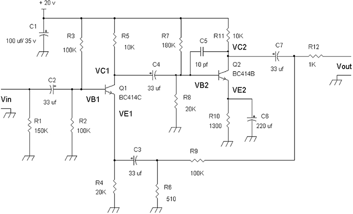
FIGURE 10.3 An example two-stage feedback amplifier with the first stage transistor with Q1 similar to the difference amplifier shown in Figure 10-2.
Let’s first find the DC bias voltages. VB1 = 10 volts DC since R3 and R2 form a divide by two voltage divider circuit for +20 volts. For an estimate as long as R2 || R3 ≤ 10 × R4, we can ignore base currents as long as β >> 10 (e.g., the β > 300 for both Q1 and Q2).
With VBEQ1 = VB1 – VE1, VE1 = VB1 – VBEQ1 or VE1 = 10 v –0.7 v or VE1 = 9.3 volts. From this, Q1’s DC collector current ICQ1 = IEQ1 = 9.3 v/20KΩ = 0.465 mA. Thus, VC1 = 20 v – ICQ1 × R5 = 20 v – 0.465 mA × 10KΩ or VC1 = 20 v – 4.65 v, which leads to VC1 = 15.35 volts.
Note that although we are not optimized for maximum swing, it will be fine because the voltage gain of the next stage is very high and less than 1 volt peak to peak swing from Q1’s collector will do. Also note VCEQ1 = VC1 – VE1 = 15.35 v – 9.3 v = +6.05 volts, which is good since the collector to emitter voltage should typically > 0.5 volt to ensure that Q1 is operating as an amplifying device.
For Q2, the base voltage is VB2 = 20 v [R8/(R8 + R7)], and thus:
VB2 = 20 v [20K/(20K + 180K)] = 20 v [20K/200K] = 20 v /10
VB2 = 2 volts, and since VBEQ2 = 0.7 volt
VE2 = VB2 – VBEQ2 = VE2 – 0.7 volt = 1.3 volts or VE2 = 1.3 volts
This means ICQ2 = IEQ2 = VE2/R10 = 1.3 v/1300Ω or ICQ2 = 1 mA.
VC2 = 20 v – ICQ2 R11 = 20 v – 1 mA (10KΩ) = 20 v – 10 v
VC2 = +10 volts
A single-supply two-transistor amplifier utilizes a difference amplifier Q1 where the emitter acts as a second input terminal for the feedback resistor network, R9 and (R6 || R4). Q1’s base can be thought of as a first input terminal. The difference voltage across the base-emitter junction of Q1 provides an output signal at the collector, VC1. This output signal is then sent to the second-stage amplifier, Q2, which is another inverting gain amplifier.
To understand this amplifier in terms of a feedback system, we can find which terminal of Q1 is the non-inverting input and which one is the inverting input. One way is to look at Q1 and Q2. We know that Q1 is a common emitter amplifier with phase inversion from the base to the collector in terms of AC signals (e.g., see Figures 10-1 left side and 10-3). Since the second stage with Q2 is also a common emitter amplifier, it inverts the phase from Q1’s collector signal. Thus, from the base of Q1 to the collector of Q2, we get two 180-degree phase inversions so that the output signal at Vout is in phase with the input signal Vin.
For Figure 10-3’s amplifier, we can say that Q1’s base terminal is a non-inverting input. By process of elimination, is the remaining input at the emitter the inverting input for this two-transistor amplifier? Yes, that is the case. If we couple an input emitter terminal AC signal at the emitter of Q1 via C3, the collector voltage VC1 will have an AC signal in the same phase with this emitter terminal input signal. Since Q1’s collector signal is sent to Q2, which is a common emitter amplifier, there will be a phase inversion from the collector signal of Q1 to the collector signal of Q2.
In other words, since a signal coupled to the emitter terminal at Q1 has the same phase as the collector signal at Q1, the phase is thus inverted from the Q1 emitter terminal signal to the collector of Q2, which is coupled to Vout. Thus, the emitter terminal of Q1 is an inverting input terminal for this amplifier.
We can estimate the non-inverting gain by just observing that the two-resistor feedback network R9 and R6 looks like the feedback network used in non-inverting gain op amp circuits. For a more accurate estimate we can replace R6’s value with R6 || R4.
However, since R4 (20KΩ) >> R6 (510Ω) we can say that (R4 || R6) ~ R6 = 510Ω.
The estimated (closed loop) gain is then [1 + (R9/R6)] ~ Vout/Vin, providing the total (open loop) gain from the first and second stages is >> [1 + (R9/R6)].
For this example, R9 = 100KΩ and R6 = 510Ω, so our estimated gain is Vout/Vin ~ [1 + (100K/510)] or Vout / Vin ~ 197.
The quick analysis of the gain of the first stage involving Q1 is about:
(R5 || R7 || R8 || Rin2) / R6, Given R5 = 10KΩ, R7 = 180KΩ, R8 = 20KΩ, and Rin2 ~ 10KΩ when Q2’s β ~ 400 at ICQ2 = 1 mA collector current
To calculate Rin2, with ICQ2 = 1 mA, re2 = 0.026 v/ICQ2 = 0.026 v/0.001 A = 26Ω. Or re2 = 26Ω. Rin2 = β re2 = 400 × 26Ω or Rin2 = 10.4kΩ or Rin2 ~ 10kΩ.
The gain of the first stage is about (R5 || R7 || R8 || Rin2)/R6 ~ 4K/510 ~ 8.
Note VB2 ~ 2 volts, so VE2 ~ 1.3 volts and with R10 = 1300Ω, the emitter and collector currents of Q2 is ~ 1.3 volts/1300Ω or ~ 1 mA = IC2. The second stage’s gain from the base of Q2 to its collector is about R11/re2, where R11 = 10kΩ with re2 = 0.026 volt/IC2 re2 = (0.026 volt) / (0.001 A) or re2 = 26Ω.
Gain of the second stage = ~ 10KΩ/26Ω or about 380.
Total open loop gain is then = gain of 1st stage × gain of 2nd stage = 8 × 380 ~3040. The estimated “closed loop” gain is ~ 197 and so we should be OK since 3040 >> 197. Should the open loop gain be in the order of [1 + (100K/510)], such as the gain of 1st stage × gain of 2nd stage = 197, the actual gain Vout/Vin will be less than than [1 + (100K/510)] = 197.
Also note that the gain calculations are estimates, by which we mean if the measured gain is within 20 percent of the calculated value, that’s good enough. Estimates within 20 percent are good enough for troubleshooting. If more accurate analysis is needed probably the best thing to do is to run a simulation via a program such as LT Spice if you are not into deep engineering analysis via hand calculations. See link to LTSPICE from Analog Devices (http://www.analog.com/en/design-center/design-tools-and-calculators/ltspice-simulator.html).
Before we look at the specific Dynaco PAT-5’s voltage regulator and low-level preamp circuit, we should examine the emitter follower circuit. See Figure 10-4.

FIGURE 10.4 An emitter follower circuit on the left side, and on the right side a block diagram model of the emitter follower circuit for AC signals.
An emitter follower circuit is often used as a gain of 1 buffer amplifier to provide a high-resistance input (Rin1) and a low-resistance output (Rout_E1).
The input resistance Rin1 ~ β re + (β + 1)(R1 || RL1), where re = 0.026 v/IC wherein IC is the DC collector current.
And the output resistance from Q1’s emitter terminal before being connected to R1 and RL1 is Rout_E1 = [Rs1/(β + 1)] + re.
For example, suppose Vin is an audio signal generator with a 600Ω as its source resistance, Rs1 = 600Ω, and R1 = 1130Ω so that IC = 10 mA. Then re = 0.026 v/0.010 A or re = 2.6Ω. Let Q1 = PN2222 (TO-92 EBC pin out) with β = 75, then we have the following with R1 || RL1 = 530Ω given RL1 = 1000Ω.
Rin1 ~ β re + (β + 1)(R1 || RL1) = 75 ×26Ω + (75 + 1)(1130Ω || 1000Ω)
Rin1 ~ 1950Ω + 40.28KΩ or Rin1 = 42.23KΩ
Rout_E1 = [Rs1/(β + 1)] + re = 600Ω/(75 + 1) + 2.6Ω = 7.89Ω + 2.6Ω or Rout_E1 = 10.49Ω
As we can see, indeed the input resistance, Rin1 = 42.23KΩ, is reasonably high and the output resistance, Rout_E1 = 10.49Ω, is fairly low.
One other characteristic of the emitter follower is that it has power supply rejection. That is, if there is noise or ripple from the power supplies, little of it shows up at the output, Vout_E1. For example, if there is even large amounts of noise (e.g., 1-volt peak to peak ripple) on the +12-volt supply in Figure 10-4, the emitter follower will reject essentially all of the positive supply ripple voltage at Vout_E1. If there is ripple on the negative supply (–12 v), it will be reduced via a voltage divider as seen from the –12-volt supply via R1 and Rout_E1. The resulting voltage dividing factor is Rout_E1/(Rout_E1 + R1), which is 10.49/(10.49 + 1130) ~ 0.01 ~ 1%. For example, if there is 100 mV of ripple on the negative supply for this example, then Vout_E1 will have only about 1 percent of 100 mV or 1 mV of noise at the output of the emitter follower.
NOTE: C1 has large capacitance to provide an AC short circuit (e.g., C1 is ~ 0Ω for AC signals when compared to RL1’s resistance value).
Figure 10-4 shows an example of this circuit with an extra resistor, R2, which does not affect Rin1 and Rout_E1. Collector series resistor R2 can be used as a current-limiting resistor to prevent Q1 from sourcing excessive current that may damage it. Typically, R2 has a resistance value in the order of 2.2Ω to about 100Ω to provide current limiting just in case the Q1’s emitter is shorted to ground. Also, R2 can be chosen with generally a higher-resistance value such as 510Ω to 10KΩ to act as a load for a common emitter amplifier for Q1. Care must be taken such that there is sufficient DC voltage across the collector-emitter terminals to avoid having Q1 in the saturation region, which will cause Q1 to not amplify.
Dynaco PAT-5 Low-Level Preamp Section and Power Supply
In the mid-1970s, the Dynaco corporation designed one of their last high-fidelity preamps, the PAT-5. We will look at a couple of its circuits for estimating performance and troubleshooting. See Figures 10-5 to 10-7. The design included a phono preamp section via an equalization network and a microphone channel. These figures have had their original Dynaco component reference designations renumbered for this book.

FIGURE 10.5 Dynaco PAT-5 low-level preamp section and power supply with regulator.
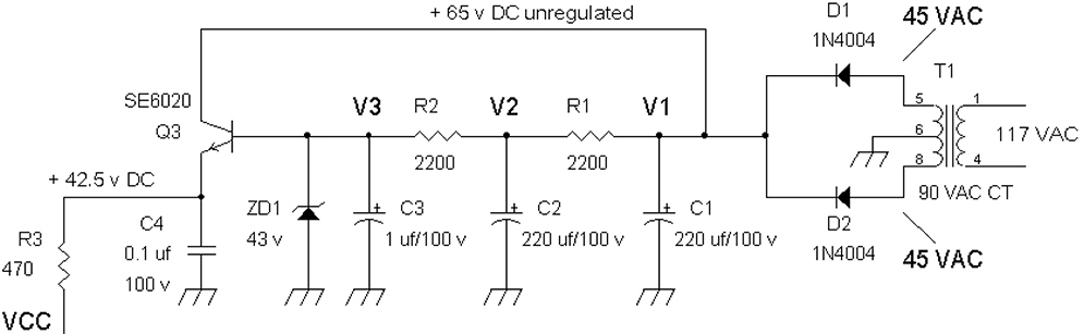
FIGURE 10.6 Power supply and voltage regulator section of the Dynaco Pat-5 preamp.

FIGURE 10.7 Preamp section of a modified PAT-5 preamp.
Let’s split Figure 10-5 into two parts—the power supply–voltage regulator and the low-level preamp section. See Figure 10-6 for the power supply–regulator section.
The power supply uses a 90-volt RMS center tapped (CT) transformer, T1, that delivers 45 VAC RMS into each diode’s anode for D1 and D2. The peak DC voltage into C1 is then 1.414 × 45 volts ~ 65 volts peak DC voltage. The cathodes of D1 and D1 provide an unregulated + 65 volts DC into capacitor C1 via the full-wave rectifier circuit of D1 and D2. R1 and C2 form a low-pass filter that removes most of the ripple (e.g., a 120 Hz sawtooth waveform for the 60 Hz transformer T1). A quick approximation for the cut-off frequency requires having R2 in parallel with R1 because ZD1, a 43-volt Zener diode, is turned on and for practical purposes the ripple voltage at ZD1’s cathode is nonexistent. Thus, ZD1’s cathode looks like an AC ground for R2 connected to C3. To find the cut-off frequency in a low-pass filter, we have to look at not only the driving resistor into C2 but also any resistor connected to C2 whose other end goes to AC ground. When we have this, the actual RC time-constant of the circuit is τ = (R1 || R2) C2 and the cut-off frequency fc = 1/[2 π τ] = 1/[2 π (R1 || R2) C2] = 1/[2 π (1100Ω) 220 μf] or fc = 0.66 Hz. For a rough estimate of how much the 120 Hz is attenuated we just take the ratio of the two frequencies, fc / 120 Hz = 0.66 Hz/120 Hz = 0.0055 or 0.55 percent of the ripple voltage from the +65-volt unregulated supply. For example, if there is a 1-volt peak to peak 120 Hz sawtooth waveform at +65 volts, then we can expect about 0.55 percent of 1 volt or about 0.55 mV of ripple on the + terminal of C2. Because R1 and R2 have equal resistances, they form an averaging voltage summing circuit. Whenever you have two equal resistors and there are two different voltages, V1 and V2, driving each resistor, the voltage at the junction of the two resistors are (V1 + V2)/2. We have 65 volts at C1 and R1, and 43 volts at R2 and C3. Thus, the estimated voltage at C2 is (65 v + 43 v)/2 or + 54 volts DC at C2’s positive terminal. Put it another way, the voltage at C2 should be the halfway point of the two voltages on each side of C1 and C3.
Transistor Q3 forms an emitter follower circuit with 43 volts at its base terminal from ZD1. We will lose about 0.7 volts due to the VBE or base emitter turn-on voltage. So, at Q1’s emitter we would expect something like 42.3 volts. Q1’s emitter can then provide about 42.3 volts at high currents while allowing ZD1 to be turned on. For example, the Zener diode current is approximately the voltage between R1 and R2 divided by (R1 + R2). This current is then (65 v – 43 v)/(R1 + R2) = 22 v/(2200Ω + 2200Ω) or ZD1’s current = 5 mA. If we have 1 mA of base current from Q3, the Zener current will be reduced to 4 mA, which is still good for turning on ZD1. However, with 1 mA of drive into the base of Q3, and with Q3 having a β ≥ 50, at least 50 mA can be provided via Q3’s emitter output terminal to the preamp circuits.
Capacitor C4 (0.1 μf) does not reduce any residual 120 Hz ripple voltage because the capacitance is too small. However, it does get rid of any higher-frequency noise, and C4 also “stomps” out any chance for Q3 to parasitically oscillate at very high frequencies (e.g., > 10 MHz). Further low-frequency filtering is provided by R3, which is coupled to C5, 100 μf at the preamp. (See Figure 10-5.)
Troubleshooting the Power Supply and Regulator
1. Confirm that the Zener diode, diodes, transistor, and capacitors are installed correctly. For example, if a 43-volt Zener diode is put in backwards, you will get a “fake” Zener voltage of 0.7 volts instead of the correct 43 volts. Remember in a Zener diode, the positive voltage via a resistor or current source will flows into the cathode. A transistor installed backwards, such as having its collector and emitter terminals reversed, may turn into a 7-volt Zener diode and it may have excessive base current due to running the transistor in reverse β mode. For example, the reverse β mode or reverse current gain mode in a transistor results in the current gain dropping to about 1 to 5, whereas a transistor normally has a current gain of over 30.
2. For your safety, be sure to avoid areas where the AC power line voltage comes in such as the power switch and or the primary windings of T1, the power transformer.
3. With the power turned on, confirm with a volt meter (negative or black lead at ground) that on the anode of D1 and D2 that there is about 40 AC volts RMS to 50 AC volts RMS. Most DVMs will measure AC in RMS voltages.
4. Then with the volt meter set to DC measurements, confirm that there is about 65 volts DC on C1’s positive terminal. If the DC voltage is low, the capacitor may be old and have lost capacitance. Parallel a ≥ 220 μf 100-volt (extra) external capacitor with C1 and see if the DC voltage rises to about 65 volts. If the voltage is restored to about 65 volts, replace C1 with the external capacitor. Note that C1 can actually be 220 μf to 470 μf at 100 volts or more. Be careful to discharge the extra external capacitor by connecting across a 47KΩ to 220KΩ resistor for about a minute. If you short out the extra capacitor to discharge it, you will encounter a large spark, which may be unsafe.
5. Measure the DC voltage at C2’s positive terminal. It should be higher than 43 volts (e.g., ≥ 50 volts DC) if there is about 65 volts at C1’s positive terminal. Then confirm that there is about 43 volts at C3, anode of ZD1, and the base of Q3. If this is confirmed, Q3’s emitter should have about 42.3 volts. You should also confirm that Q3 has a base-to-emitter DC voltage of about 0.7 volt. If the voltages are lower than expected at the base-to-emitter of Q3, then confirm there is about 65 volts at the collector. If Q3 does not have collector voltage > 43 volts, then the base-emitter junction acts like a diode, and excessive base current will be drawn because Q3 is not acting like an emitter follower circuit having a high-input resistance at the base. Also, if the base-to-emitter voltage is greater than 0.7 volts, such as VBE > 1 volt, then Q1’s base-to-emitter junction may be blown, which results in an open circuit. You will need to replace Q3 and a suitable NTE replacement part is found via http://www.nteinc.com/index.php.
6. If the voltage at Q1’s emitter is too high, that is, greater than the Zener voltage, 43 volts, then there could be a short across the collector-to-emitter junction of Q3. You will need to replace Q3.
7. Generally, if the Zener diode is damaged, it can be shorted out, which can result in 0 volts at the base and emitter of Q3. If the Zener diode is an open circuit, Q1’s base voltage will be higher than 43 volts.
8. Measure the DC voltage across R3 (470Ω), which should be a few volts DC at most. If the voltage across R3 has over 6 volts, then the preamp may be drawing excessive current via C5 or other circuits.
Now let’s look at the preamp section in Figure 10-7.
This preamp has two feedback loops. One is a DC bias feedback loop that includes R15, R11, R9, and R8. The second is an AC signal feedback loop via R19 and R10 when Switch 1 is at position “3” (microphone), and also with C10, C11, R16, R17, and R10 when Switch 1 is at position “1” (phono cartridge).
Preamp’s DC Bias Point Estimates
We will look at the DC feedback loop first. Q1 by itself is a common emitter amplifier, which means the collector of Q1 has an inverted phase relative to the input signal into its base. In Figure 8-19 of Chapter 8 we saw a common emitter amplifier with a feedback resistor (R_BC) from collector to base that sets up the collector current of the transistor (along with base to ground resistor R_BE in Figure 8-19). When we look at Figure 10-7 we notice that Q1’s collector is coupled indirectly back to its Q1 base by a “circuitous” route through Q2. This route starts from Q1’s collector connected to the base of Q2, and then via the emitter of Q2 by way of R14 and R15, a feedback network of R11 and R9 feeds a DC signal back to the base of Q1 via R8.
In terms of DC biasing, Q2 is an emitter follower amplifier for Q1’s collector output. Since an emitter follower has no phase inversion from base to emitter of Q2, we can connect a feedback resistor R11 back to the base of Q1 (via R8). Resistor R9 forms a voltage divider with feedback resistor R11. Notice that R11 is connected to C8, a large capacitance capacitor to “completely” filter out any AC signal via Vin such that only a DC signal voltage is fed to R11 to work properly for the DC feedback loop. In Figure 10-6 we can estimate VCC ~ 40 volts for a few volts drop across R3.
Let’s look at estimating Q1’s collector current. It is important to note that Q1’s collector (VC1) is connected to Q2’s base. We first want Q1’s collector voltage, VC1, to be much less than one-half of VCC ~ +40 volts. The reason for this is to maximize voltage swing at Q2’s collector output. Ideally, we want the base voltage of Q2 to be sitting at a low voltage such as less than 6 volts, but high enough to bias Q2’s base-emitter junction and provide sufficient voltage at R15 to bias Q1’s circuitry via base resistor R8. An example of a “bad” design would have the collector DC voltage at Q1 at +35 volts. Given that we have a 43-volt supply, this would mean Q2’s collector can swing only from 35 volts to 43 volts, which is about 8 volts peak to peak. However, a better design having Q1’s DC collector voltage at 6 volts instead means that Q2’s output can swing from 6 volts to about 43 volt or about 37 volts peak to peak, which is much better than having an 8-volt peak to peak swing.
Let’s assume that VC1 is in the order of 5 volts to 10 volts so that the DC voltage at the base of Q2 will allow good output voltage swing at Q2’s collector. Recall that the collector voltage should always be above the base voltage. The collector current ICQ1 = (VCC – VC1)/R12. If we pick a guess of VC1 = 6 volts, then:
ICQ1 = (40 v – 6 v)/27KΩ or ICQ1 ~ 1.26 mA
NOTE: If we had guessed that VC1 = 10 volts instead, then ICQ1 ~ 1.11 mA, which is not much of a difference from 1.26 mA.
Now we can estimate Q1’s DC emitter voltage as:
VE1 = ICQ1 × R10 ~ 1.26 mA × 470Ω or VE1 = +0.59 v DC
We can estimate that the VBE turn on voltage of Q1 and Q2 is about 0.7 volt.
Because the DC current gain for Q1 is very high, we can “ignore” base currents flowing through R8, so there is almost no voltage drop across R8. Thus, Vb1 ~ Q1’s base voltage. In practice if Q1’s β ~ 400 and Q1’s collector current ~ 1.26 mA, its base current is about 1.26 mA/β or about 3.15 μA. The voltage drop across R8 is then 100kΩ × 3.15 μA or about 0.315 volt.
Q1’s DC base volts ~ Vb1 = VBEQ1 + VE1 ~ 0.7 v + 0.59 v or Vb1 ~ 1.29 volts.
We can now find V_R15 via a voltage divider formula:
V_15 [R9/(R11 + R9)] = Vb1
Or V_R15 = Vb1/{[R9/(R11 + R9)]} = Vb1[(R11 + R9)/R9]
V_R15 = Vb1 [ (R11/R9) + 1]
With Vb1 = 1.29 volt, R9 = 10KΩ, and R11 = 18KΩ, we have for V_R15:
V_R15 = 1.29 v [ (18K/10K) + 1] = 1.29 v [1.8 + 1] = 1.29 v [2.8] or V_R15 = 3.6 volts
Thus, ICQ2 = V_R15/R15 = 3.6 volts/2200Ω or ICQ2 = 1.64 mA.
And this means VC2 = VCC – ICQ2 × R13 ~ (40 v – 1.64 mA × 10KΩ) VC2 = (40 v– 16.4 v) or VC2 = 25.6 volts DC.
The estimates for the bias points can be given a ± 20 percent tolerance. We are not after the exact values but something within the “ballpark.” In some cases, you can find the schematic or service manual to high-fidelity product on the web. One such site, www.hifiengine.com, requires login information including email address and password. See Table 10-1 from the calculated values versus information from the Dynaco PAT-5 Preamplifier’s construction and service manual.
TABLE 10.1 Estimated Calculations Versus Service Manual’s Information, Which Are Within About 20 Percent
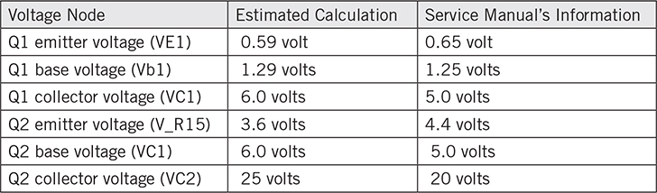
Making estimates of the DC bias points can be handy because the service manual or schematic may not always be available. You may have to “manually” draw out a schematic by tracing the circuit you are troubleshooting. From that, many discrete amplifiers can be analyzed quickly either by making estimates as shown here, or by entering the schematic into a simulation program such as SPICE. You can download a free version from Analog Devices via the following link: http://www.analog.com/en/design-center/design-tools-and-calculators/ltspice-simulator.html.
AC Analysis
For looking into the small signal gain of Figure 10-7, we notice that there is an AC feedback path via Q2’s collector to R10 at the Q1’s emitter either through C10, C11, R16, R17, or through R19. In the larger scheme of things, Q1’s base is like the non-inverting input terminal of an op amp or feedback amplifier, while Q1’s emitter terminal is like the inverting input terminal. In the simplest case where Switch 1 selects position 3 (for microphones) to utilize R19 and R10 as the feedback elements, the gain of the preamplifier is Vout/Vin ~ [1 + (R19/R10)]. If this equation looks familiar, it is the same equation for calculating voltage gain for an op amp circuit for a non-inverting amplifier. With R19 = 68KΩ and R10 = 470Ω, Vout/Vin ~ [1 + (68K/470)] or Vout/Vin ~ 145.
With Switch 1 set for phono preamp, the feedback network C10, C11, R16, and R17 works like a frequency dependent “resistance.” This feedback network complies to the RIAA phono equalization curve. This network is more properly termed as an impedance network. At high audio frequencies the two capacitors will dominate the impedance characteristic and act like a low-value impedance. We can model this network to give an idea of what we would expect the gain to be as a function of frequency. Also, with a signal generator and oscilloscope you can confirm the following:
Vout/Vin ~ [1 + (Znetwork/R10)]
where Znetwork is a combination of C10, C11, R16, and R17.
At a low frequency such as 20Hz, the capacitors have very high impedances and the resistors dominate so Znetwork ~ R16 + R17 = 27KΩ + 470KΩ = 497KΩ. Thus, at around 20 Hz, the expected gain within about 20 percent is Vout/Vin ~ [1 + (497K/470)] ~ 1000. Try setting the generator at 10 mV peak to peak at 20 Hz for Vin, and Vout should be about 10 volts peak to peak within 20 percent.
To find what we may expect at 1000 Hz, we can look at the RIAA feedback network and pick out R16 at 27KΩ as the resistor value we will use to find the gain. This means at 1000 Hz the gain will be [1 + (27K/470)] = 58.4 within 20 percent. The actual gain may be slightly higher, like 70. Again, you can set the generator at 1000 Hz with 50 mV peak to peak at Vin and Vout should be about 2.9 volts to 3.5 volts peak to peak.
Finally, at 20 kHz, the RIAA equalization curve requires that the gain is dropped to 10 percent of the 1000 Hz gain. So, at 20 kHz we will expect Vout/Vin ~ 5.84 within 20 percent. Again, set the generator to about 100 mV peak to peak at 20 kHz for Vin, and Vout should be about 0.6 volt peak to peak within 20 percent. If Vout is around 0.75 volts peak to peak, that’s fine too.
Another way to test this is: Set the generator to about 10 mV RMS or about 28 mV peak to peak at Vin, and test at 20 Hz, 1000 Hz, and 20 kHz and note Vout’s amplitude. At 20 Hz, the amplitude should be about 10x of the output at 1000 Hz. And at 20 kHz, its amplitude should be about 10 percent or one-tenth of the amplitude of the 1000 Hz signal.
Troubleshooting the Preamp in Figure 10-7
• Make sure there is about +40 volts DC from the power supply to C5 and then check for the DC bias points listed on Table 10-1. If the DC voltages are within about 20 percent, then the preamp is ready to be tested with AC signals.
• If there are DC bias problems, with a DVM, check the VBE (base to emitter) turn-on voltage for transistors Q1 and Q2. Typically, this should be between 0.6 volt and 0.7 volt. If you still have problems and the DC voltages are incorrect per Table 10-1, inspect each of the transistors to make sure the pin outs for emitter, base, and collector are connected correctly. For example, if any of the transistors are connected in reverse, where the collector and emitter terminals are reversed, the β will drop from about 400 or 500 to 1 to 5, which will cause excessive base currents to be drawn. If there is excessive base current from Q1, the DC voltage across resistor R8 will be large, since typically with a β ≥ 400, the voltage across R8 will be < 0.5 volt. If Q1 is wired with collector and emitter reversed, the voltage across R8 will be >> 0.5 volt.
• Check that all electrolytic capacitors are installed correctly polarity-wise. An incorrect installation in electrolytic capacitors will cause capacitor leakage currents, which can “throw off” the DC bias voltages.
• With a signal generator at 1000 Hz sine wave and 50 mV peak to peak for Vin, select Switch 1 for phono operation, and confirm that Vout has about 60 to 75 times the input amplitude or 3 volts to 3.75 volts peak to peak. You can probe Q2’s base to verify that you get about 100 times less amplitude of the 1000 Hz signal than at the collector. The gain of the second stage Q2 is ~ R13/R14 = 10K/100 ~ 100 within 25 percent. So expect Q2’s base to have about 30 mV of signal. Note that R15 is AC shorted to ground via C8. Confirm that there is no 1000 Hz sinewave signal C8 (220 μf) with an oscilloscope set at 10 mV per division sensitivity and 500 μsec per division. You should get close to a flat line at this oscilloscope setting. If there’s an AC signal at C8’s plus terminal, replace it with a new 220 μf capacitor of at least 50 working volts. Also confirm that Q1’s emitter terminal has almost the same AC amplitude voltage as Vin. Note that Q1’s base and emitter terminals are like the (+) and (–) inputs to an op amp, which have the same AC voltage (e.g., virtual short circuit across the inputs) when negative feedback is applied.
• If Vout seems to have some high-frequency parasitic oscillation, check or replace C7 (47 pf) since this capacitor is used to ensure that this preamplifier is stable with feedback components ( R16, R17, C10, and C11).
• If the Vout’s signal is clipped, check the load resistance value, which typically should be ≥ 10KΩ. A typical audio power amplifier has at input load resistance in the range of 10kΩ to 250kΩ. If the preamp’s output is loading into a headphone or resistor in the 1KΩ range, then Vout will clip at voltages < 3 volts peak to peak. Again, this preamp is not meant to drive earphones or headphones. The Q2 output stage can only deliver about a milliamp or two.
A High-Fidelity Audio Power Amplifier
Now let’s look at a SX-636 Pioneer stereo receiver power amplifier. Although this is a 1970s amplifier design, the circuit topology still held up into the early 2000s. Many of the newer designs still include its basic features, a differential pair input stage and a complementary push pull output stage. We will explore some of the sub-circuits in this amplifier including the input stage, the second voltage gain stage, and its output stage.
As engineers learned how to design with transistors, they migrated from earlier circuit topologies that included audio signal transformers to output transformer-less designs using output capacitors (e.g., 2200 μf) to direct DC coupled output stages. The SX-636 stereo receiver’s design used positive and negative power supplies, and in essence, it is almost like a high-power output op amp. See Figure 10-8.
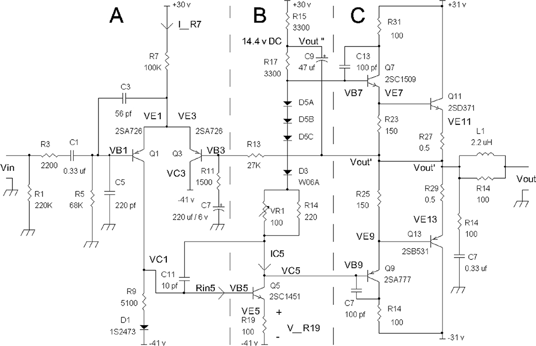
FIGURE 10.8 A redrawn full-page schematic of the Pioneer SX-636 audio power amplifier. Sections A = first stage differential pair, B = second stage voltage gain amplifier, and C = output stage to supply large currents to a loudspeaker.
Most power amplifiers include two-stage preamplifiers, and this circuit is no exception. In place of a single transistor difference amplifier from Figure 10-7 Q1 (BC414C) where Q1’s base is the (+) input terminal and its emitter is the (–) input terminal, we have in Figure 10-9 transistors Q1 and Q3 where the Q1’s base is the (+) input terminal and Q3’s base is the (–) input terminal.
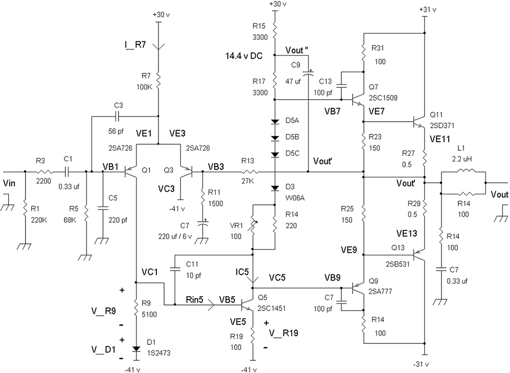
FIGURE 10.9 SX-636 power amplifier schematic.
In Figure 10-9, Q1 and Q3 form a “true” differential amplifier where the input resistance input into each base is the same. Recall that in a single transistor difference amplifier, the input resistance into the base is much greater than the input resistance into its emitter by a factor of β. Note: Start with confirming all supply voltages.
We can observe that the emitter-to-base voltages of Q1 and Q3 are both approximately 0.7 volts. From this we can also surmise that the DC voltage across VB1 and VB3 is ~ 0 volt since VB1 = VBEQ1 + VEBQ3 + VB3, or VB1 – VB3 = VBEQ1 + VEBQ3.
However, VBEQ1 = –VEBQ1, thus VB1 – VB3 = (–VEBQ1 + VEBQ3). Since the emitter base turn-on voltages of PNP transistors Q1 and Q3 are both ~ 0.7 volt, so VEBQ1 = VEBQ3 = 0.7 v. And this means the difference voltage between the two bases is VB1 – VB3 = –0.7 v + 0.7 v, or VB1 – VB3 = 0 v, which also leads to VB1 = VB3, which is the same approximation for an operational amplifier circuit with negative feedback where the (+) and (–) inputs are about the same voltage. The output of the Q1 and Q3 amplifier is VC1 that feeds the amplified signal to the second stage, Q5, a common emitter amplifier. The output signal from Q5’s collector (VC5) is then fed to a two-stage complementary transistor emitter follower with the first emitter follower stage formed by Q7 and Q9, and whose second stage emitter follower circuit includes Q11 and Q13, which are high-current output transistors that are mounted on a heat sink. Q7, Q11, Q13, and Q9 biasing diodes are D5A-D5C and D3. These diodes are also on the heat sink with output transistors Q11 and Q13. Diodes D5A-D5C and D3 then track the temperature of the output devices and prevent Q11 and Q13 from heat damage. For example, if the output transistors heat up, diodes D5A-D5C and D3 will also heat up and provide a lower biasing voltage to the output transistor, therefore reducing the output transistors’ DC quiescent collector current and thus reducing power dissipated (e.g., which lowers the temperature) in the output devices Q11 and Q13.
DC Biasing Conditions in Figure 10-9
Q1 and Q3 form a differential pair amplifier where it is the difference in voltage between their two bases that provides an amplified output at Q1’s collector, VC1. To bias the differential amplifier, resistor R7 provides an emitter tail current to Q1’s and Q3’s emitter. Ideally, when with no signal, Vin → 0 volt AC, we want the tail current I_R7 to split evenly between Q1 and Q3. Reminder: Confirm all supply voltages.
When Vin → 0 volt AC, Q1’s base voltage, VB1 ~ 0 volt DC. If VB1 ~ 0 volt, then VE1 ~ 0.7 volt since in a PNP transistor the turn-on voltage is 0.7 volt from emitter to base (VEB ~ 0.7 volt).
The emitter tail current is then the current flowing through R7, I_R7 = [(30 v – 0.7v)/R7] = I_R7. With R7 = 100KΩ, we have I_R7 = (29.3 v)/100KΩ or I_R7 = 0.293 mA. With the tail current 0.293 mA, we have split evenly this current between the collector currents of Q1 and Q3. This means that Q1’s collector current IC1 is one-half of the emitter tail current I_R7, so IC1 = 0.1465 mA.
With Q1’s collector current known, we can take a look at the second stage, Q5’s DC biasing conditions. Q5’s collector needs to draw enough current via IC5 such that at the base of Q7, VB7, we have about +1.4 volts, which is the sum of the VBE turn-on voltages for Q7 and Q11. The reason for having this +1.4 v = VB7 is so that by the time we measure Vout, we should get close to 0 volts DC. For example, a large DC voltage of 10 volts DC at Vout can burn out an 8Ω loudspeaker with about 1.25 amps DC flowing through the speaker’s voice coil.
Q5’s collector current, IC5 = (30 v – 1.4 v)/(R15 + R17). With R15 = R17 = 3300Ω, IC5 = 28.6 v/(3300Ω + 3300Ω) or IC5 = 4.33 mA. Now that we know that IC5 ~ 4.33 mA, we would deduce that the voltage across R19, V_R19, which is Q5’s emitter resistor, should be IC5 × R19 or about 0.00433 A × 100Ω = 0.433 volt across R19, a 100Ω resistor.
The total voltage across Q5’s base emitter junction and R19 = VBEQ5 + V_R19 ~ 0.7 v + 0.433 v = 1.133 volts. This total voltage having VBEQ5 + V_R19 = 1.133 volts is also equal to the voltage across R9, V_R9 plus the voltage across D1, V_D1. Because IC1 ~ 0.1465 mA, the forward voltage across D1, V_D1 ~ 0.4 v. You can download the spec sheet for the 1S2473 diode for D1.
This means V_R9 + V_D1 = VBEQ5 + V_R19 = 1.133 volts.
Or V_R9 = 1.133 v – V_D1 = 1.133 v – 0.4 v, or V_R9 ~ 0.733 volt.
So, does IC1 × R9 = 0.1465 mA × 5100Ω = 0.733 volt? Let’s see.
0.1465 mA × 5100Ω = 0.747 volt
which is pretty close to 0.733 volt.
So, based on working “backwards” from Q5’s collector current for 0 volts at Vout, we see that the voltage driving into the base of Q5 via Q1’s collector voltage VC1 is close but not “exact.” As we will see, this amplifier is part of a negative feedback system that will adjust VC1 “precisely” to the correct DC voltage such that Vout = 0 volt DC.
So, how does the amplifier circuit “guarantee” that Vout will have 0 volts DC when Vin = 0 volt? What if the transistors, Q5, Q7, and Q11, really do not have 0.7-volt VBE base-to-emitter voltages? Wouldn’t we have a DC offset problem at Vout? Fortunately, the amplifier is set up as a unity gain feedback amplifier or voltage follower for DC signals. That is, for DC voltages, you can remove C7 for DC analysis. Now the amplifier looks very much like a voltage follower op amp circuit with R13 as the feedback resistor. So, the amplifier achieves near 0-volt DC at its output due to Vout’ being connected back to the inverting input terminal (Q3’s base) via R13.
Since the differential amplifier Q1 and Q3 and second-stage amplifier Q5 provide “high” DC gain, Figure 10-9’s circuit looks like one “big” discrete op amp of sorts. Thus, by negative feedback, the DC output voltage is very close to 0 volt, because the (+) input (Q1’s base) is set to ~ 0-volt DC, which then drives via feedback resistor R13 to cause the (–) input voltage at Q3’s base to go to → 0 volt. Thus, Vout’ and Vout both go to 0-volt DC. (At Vout, inductor L1 = 0Ω for DC currents.)
One of the most important DC conditions to look for is the bias voltages for the driver transistors Q7 and Q9 and the output transistors Q11 and Q13. Biasing diodes D5A – D5C in series with another biasing diode D3 should provide about +2.5 volts from the base of Q7 (VB7) to the cathode of D3. VR1 and R14 supply additional voltage in series with the biasing diodes such that you can set the output transistors’ quiescent bias current. To do this, Vin is removed. Then measure with a volt meter across either output transistor emitter resistors R27 or R29 and adjust VR1 for about 0.025 volt to 0.038 volt so that the output devices are idling at 50 mA for “normal biasing” or at 76 mA for lower crossover distortion.
NOTE: The total DC biasing voltage for the driver and output transistors is VBEQ7 + VBEQ11 + VEBQ13 + VEBQ9 ~ 0.7 v + 0.7 v + 0.7 v + 0.7 v = 2.8 volts.
AC Signal Conditions
For signal tracing this amplifier, we will need an oscilloscope and sine wave generator. Also, because this is indeed a power amplifier, an 8Ω load resistor rated at 40 watts or more will be connected to the output, Vout. You can improvise by connecting eight 1Ω 5-watt resistors in series or parallel six 47Ω 10-watt resistors. Although 8Ω loads are commonly used for evaluating power amplifiers, you can also use resistive loads in the 4Ω to 16Ω range at the appropriate wattage ratings of at least 40 watts. Alternatively, a 100-watt incandescent light bulb can be used and it will have about 10Ω (cold) resistance, but the resistance will go up as the lamp glows brighter.
If the DC conditions are correct in that Vout ~ 0-volt DC, you can first test the amplifier without any load resistor. Set the sine wave generator for 1 volt peak to peak at 400 Hz. The AC gain should be Vout/Vin = [1 + (R13/R11)] or [1 + (27K/1500)] = Vout/Vin = 19. This means Vout = 19 × 1 volt peak to peak or Vout = 19 volts peak to peak 400 Hz sine wave.
Now with the oscilloscope, you should be able to also measure about 19 volts peak to peak sine wave at VB7, VB9, and at C9’s positive terminal, Vout".
The gain of the second stage, Q5, may look “obvious” because the collector load resistors, R15, in series with R17 may look like the total load resistance of R15 + R17 = 3300Ω + 3300Ω = 6600Ω. The DC load resistance is 6600Ω for Q5 and the DC gain from VB5 to VC5 ~ 6600Ω/R19 = 6600/100 = 66. However, the AC load resistance is much higher due to AC coupling capacitor C9, which is also known as a “bootstrap” capacitor. Capacitor C19 has two functions. First, it provides a same phase signal from Vout back to R17 for providing extra signal during the positive cycle of the sine wave such that there is increased current drive into Q7 and Q11.
Without C9, the amplifier will clip prematurely at the positive cycle of the sine wave. The second function of C9 is to boost the AC load resistance for Q5’s collector. We can estimate the collector load’s AC resistance due to C9 and R17, which will result in something >> R17. For a very rough approximation, the AC signal is identical at both terminals of R17, which are at Vout” and VB7. With “equal” AC voltages at both ends of R17 no AC current flows through R17, and this results in an infinite AC resistance for R17. However, there is a slight loss at Vout and Vout” compared to the AC signal at Q5’s collector. The two-stage emitter followers from Q7 and Q11 form a gain of about 0.8 to 0.9 gain. That is Vout/VB7 ~ 0.8 to 0.9. The bootstrapping effect from C9 that couples the output signal Vout back to R17 will raise the effective collector load resistance for Q5 in the following manner: Q5’s load resistance ~ R17/[1 – (Vout/VB7)]. So, if Vout/VB7 ~ 0.9, then Q5’s load resistance ~ 3300Ω/[1 – (0.9)] = 3300Ω/0.1 = 33,000Ω, and the approximate AC gain from Q5 is about 33,000Ω/R19 = 33,000/100 = 330. Note that R19 = 100Ω.
Compared to the DC gain of 66, the AC gain of 330 is 5 times higher due to the bootstrapping capacitor. The actual AC gain from VB5 to VC5 will be at least twice the gain of 66 but likely less than 500 when loaded with an 8Ω load at Vout. If the gain is around 66 or less, then C9, the bootstrapping capacitor, has lost capacitance and needs to be replaced. For example, if the output voltage is 19 volts peak to peak at 400 Hz sine wave, then VC5 should also have about 19 volts peak to peak; and the VB5 should have < (19/66) volt peak to peak, which is < 287 mV volt peak to peak at Q5’s base. Note that in this example, VB5 ~ 19 volts/AC gain, and if the AC gain is estimated to be at 330, then VB5 ~ 19 volts/330, or VB5 ~ 57.5 mV peak to peak (which is less than 287 mV peak to peak).
NOTE: The diodes D5A to D5C and D3 form a low AC resistance ≤ 50Ω because they are being used as a constant voltage source, which by definition has ~ 0Ω AC resistance. The maximum resistance by VR1 in parallel with R14 is about 70Ω.
Troubleshooting the Power Amplifier
1. With the power turned off, check the resistances from collector to emitter of the output transistors Q11 and Q13. You will need to measure the collector-to-emitter resistances a second time with the probe leads reversed. Typically, if the resistances are > 10Ω, the transistors are fine. But if the collector-to-emitter resistances fall in the 2Ω or less category, chances are that there is a shorted transistor. If you find any one of the output transistors shorted, remove both output transistors Q11 and Q13. See Figure 10-10.
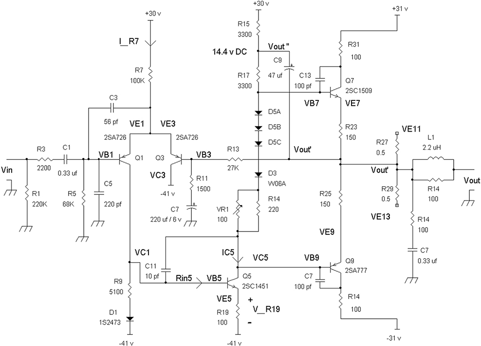
FIGURE 10.10 Schematic with output transistors removed, and driver transistors Q7 and Q9 to Vout.
Now, measure the collector-to-emitter resistances of the driver transistors, Q7 and Q9, the same way as before, twice with the second time having the ohm meter’s leads swapped. If there are no short circuits from collector to emitter of the driver transistors, you can now power up the amplifier without the output transistors, because the driver transistors will keep the negative feedback loop intact via R23 and R25 connected to feedback resistor R13. Confirm that the DC voltage at Vout is about 0 volts. Connect a 1000Ω load resistor to Vout and connect a signal generator at 1-volt peak to peak sine wave at 400 Hz to Vin. Confirm with an oscilloscope that Vout has a sine wave at about 19 volts peak to peak. If Vout does provide about a 19-volt peak to peak signal into the 1000Ω half-watt (or two 2000Ω quarter-watt resistors in parallel) load resistor, then the amplifier probably works fine up to this point and all you need is to replace the power transistors. If you cannot find the original part numbers, you can generally replace the NPN and PNP TO-3 case output transistors with parts from NTE at: http://nte01.nteinc.com/nte%5CNTExRefSemiProd.nsf/$all/72BF14B50722ACF285257910007E5A0D?OpenDocument.
Turn off the power or, better yet, unplug the power cord and replace the output transistors. Keep track of which transistor goes where. The NPN transistor will have its collector connected to the +31-volt supply line, which you can confirm with an ohm meter with the power turned off. The NPN 2SD371 can be replaced by an NTE380, MJ802, or 2N5886, and the PNP 2SB531 can be replaced with an NTE281, MJ4502, or 2N5884.
Alternatively, you can select for TO-3 case NPN and PNP power transistors that have voltage breakdown of at least 70 volts and at least a 10A collector current rating. For example, the 70-volt transistors 2N3055G (NPN) and MJ2955 (PNP) may serve as replacements. Although, to be on a safer side, the higher-voltage transistors mentioned above should be used. With the output transistors replaced, turn off the signal generator, and turn on the amplifier and measure for about 0 volts at Vout.
2. Replace the 1000Ω load resistor with at least a 25-watt 8Ω resistor. Be sure to keep the 8Ω load resistor away from other items because it will be very hot once the amplifier supplies signal to it. Turn on the generator for 1 volt peak to peak into Vin at 400 Hz. You should measure with an oscilloscope about 19 volts peak to peak across the 8Ω load resistor. Sweep the frequency from about 50 Hz to about 10 kHz and confirm about 19 volts peak to peak at the output. Now reduce the signal generator’s input voltage by half to 0.5 volt peak to peak, and sweep the generator from 50 Hz to 20 kHz to observe about 9.5 volts peak to peak at Vout.
CAUTION: Do not try to measure the amplifier at 20 kHz at full power. This test can eventually destroy the output transistors due to excessive heating. At the top end of the audio frequencies, the output power transistors become more lossy, and extra heat builds up, which can damage them.
3. In some cases, it may be difficult to find exact replacements for all the parts. Generally, it is better to replace “up” with higher power dissipation, voltage, or collector current devices. This amplifier has supply voltages of +31 volts to –41 volts. Thus, to be on the safe side, we can specify the transistors’ voltages as > (+31 v – –41 v = +31 v +41 v = 72 v) or > 72 volts. Given that the AC power line can increase as much as 10 percent, the transistors’ minimum voltage rating would be about 80 volts. For example, you can replace the input transistors, 2SA726 (BCE pin out) with careful installation using 2N5401 (EBC pin out) because the pins outs are not the same. Similarly, the pre-driver transistor, 2SC1451 (EBC), 150 volts, TO-5 case, may be replaced with TO-5 case transistors 2N3440 (EBC), 250 volts or 2N3439 (EBC) 300 volts. If there is a recommended substitution with a lower power dissipation or plastic TO-92 case transistor, it’s better to find another transistor with higher power ratings.
For transistors that begin with 2SA, 2SB, 2SC, and 2SD, sometimes the “2S” is dropped. For example, a 2SD371 may be also named D371. Or a 2SA726 and an A726 transistor are really the same electronic part.
However, it is always best to replace any broken transistor with the original part or with an NTE version. Replacing with other components can sometimes lead to parasitic oscillations. Make sure to retest the amplifier with an oscilloscope probing the output terminal, Vout, and look for any small or large high-frequency signals. If they are there, you need to go back and look for original parts.
Also, sometimes you may be able to find the exact part number replacements on eBay, but beware of counterfeit items.
This wraps up Chapter 10. Obviously, there are many more ways to examine both the PAT-5 preamp and the SX-636 power amplifier. Troubleshooting takes experience, but make sure to take safety precautions.
Chapter 11 will look into analog integrated circuits.