Domino Circuits
Static circuits built from transparent latches remove the hard edges of flip-flops, allowing the designer to hide clock skew from the critical path and use time borrowing to balance logic across pipeline stages. Traditional domino circuits are penalized by clock skew even more than are flip-flops, but by using overlapping clock phases it is possible to remove latches and thus build domino pipelines with zero sequencing overhead. This chapter describes the timing of such skew-tolerant domino pipelines and the design of individual domino gates.
3.1 Skew-Tolerant Domino Timing
This section derives the timing constraints on domino circuits that employ multiple overlapping clocks to eliminate latches and reduce sequencing overhead. The framework for understanding such systems is given the name skew-tolerant domino and is applicable to a variety of implementations, including many proprietary schemes developed by microprocessor designers. Once the general constraints are expressed, we explore a number of special cases that are important in practical designs. By taking advantage of the fact that clock skew tends to be less within a small region of a chip than across the entire die, we can relax some timing requirements to obtain a greater budget for global clock skew and for time borrowing. In fact, the “optimal” clocking waveforms provide more time borrowing than may be necessary, and a simplified clocking scheme with 50% duty cycle clocks may be adequate and easier to employ. Another interesting case is when the designer uses either many clock phases or few gates per cycle such that each phase controls exactly one level of logic. In this case, some of the constraints can be relaxed even further.
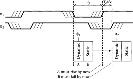
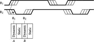
In general, let us consider skew-tolerant domino systems that use N overlapping clock phases. By symmetry, each phase nominally rises Tc/N after the previous phase and all phases have the same duty cycle. Each phase is high for an evaluation period te and low for a precharge period tp. Waveforms for a four-phase system are illustrated in Figure 3.1.
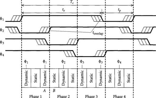
We will assume that logic in a phase nominally begins evaluating at the latest possible rising edge of its clock and continues for Tc/N until the next phase begins. When two consecutive clock phases overlap, the logic of the first phase may run late into the time nominally dedicated to the second phase. For example, in Figure 3.1, the second Φ1 domino gate consists of dynamic gate A and static gate B. Although Φ1 gates should nominally complete during Phase 1, this gate runs late and borrows time from Phase 2. The maximum amount of time that can be borrowed depends on the guaranteed overlap of the consecutive clock phases. This guaranteed overlap in turn depends on the nominal overlap minus the clock skew between the phases. Therefore, the nominal overlap of clock phases toverlap dictates how much time borrowing and skew tolerance can be achieved in a domino system.
3.1.1 General Timing Constraints
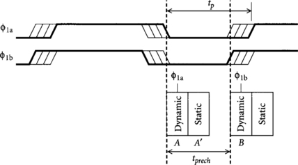
We will analyze the general timing constraints of skew-tolerant domino by solving for this precharge period, then examining the use of the resulting overlap. Figure 3.2 illustrates the constraint on precharge time set by two consecutive domino gates in the same phase. tp is set by the requirement that dynamic gate A must fully precharge, flip the subsequent static gate A,’ and bring the static gate’s output below Vt by some noise margin before domino gate B reenters evaluation so that the old result from A’ doesn’t cause B to evaluate incorrectly. We call the time required tprech and enforce a design methodology that all domino gates can precharge in this time. The worst case occurs when Φ1a is skewed late, yet Φ1b is skewed early, reducing the effective precharge window width by tskew1, which is the skew between two gates in the same phase. Therefore, we have a lower bound on tp to guarantee proper precharge:
The precharge time tprech depends on the capacitive loading of each gate, so it is necessary to set an upper bound on the fanout each gate may drive. Moreover, on-chip interconnect between domino gates introduces RC delays that must not exceed the precharge time budget.
From Figure 3.1 it is clear that the nominal overlap between consecutive phases toverlap is the evaluation period minus the delay between phases, te – Tc/N. Substituting te = Tc – tp, we find
This overlap has three roles. Some minimum overlap is necessary to ensure that the later phase consumes the results before the first phase precharges. This time is called thold, though it is a slightly different kind of hold time than we have seen with latches. Additional nominal overlap is necessary so that the phases still overlap by thold even when there is clock skew. The remaining overlap after accounting for hold time and clock skew is available for time borrowing. If the clock skew between consecutive phases Φ1 and Φ2 is tskew2, we therefore find
The hold time is generally a small negative number because the first dynamic gate in the later phase evaluates immediately after its rising clock edge while the precharge must ripple through both the last dynamic gate and following static gate of the first phase. Moreover, the gates are generally sized to favor the rising edge at the expense of slowing the precharge. The hold time does depend on the fanouts of each gate, so minimum and maximum fanouts must be specified in a design methodology to ensure a bound on hold time. For simplicity, we will sometimes conservatively approximate thold as zero.
Also, now that we are defining different amounts of clock skew between different pairs of clocks, we can no longer clearly indicate the amount of skew with hashed lines in the clock waveforms. Instead, we must think about which clocks are launching and receiving signals and allocate skew accordingly. We will revisit this topic in Chapter 5.
How much skew can a skew-tolerant domino pipeline tolerate? Assuming no time borrowing is used and that all parts of the chip budget the same skew, tskew-max, we can solve Equation 3.3 to find
For many phases N and a long cycle Tc, this approaches Tc/2, which is the same limit as we found for transparent latches in Equation 2.5. Small N reduces the tolerable skew because phases are more widely separated and thus overlap less. The budget for precharge and hold time further reduces tolerable skew. The following example explores how much skew can be tolerated in a fast system.
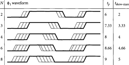
EXAMPLE 3.1
Consider a microprocessor built from skew-tolerant domino circuits with a cycle time Tc = 16 and precharge time tprech = 4 FO4 inverter delays. How much clock skew can the processor withstand if 2, 3, 4, 6, or 8 clock phases are used?
SOLUTION
Let us assume the hold time is 0. The maximum tolerable skew is computed from Equation 3.4, and the precharge period is then found using Equation 3.1. Figure 3.3 illustrates the clock waveforms, precharge period, and maximum tolerable skew for each number of clock phases. Notice that the precharge period must lengthen with N to accommodate the larger clock skews while still providing a minimum guaranteed precharge window.
In Section 5.2 we will consider various approaches for generating the clock waveforms. Ideally, te and the delay between phases would scale automatically as the frequency changes to provide the maximum tolerable skew at any frequency. In practice, it is often most convenient to generate fixed delays between phases, optimizing for tskew-max at a target operating frequency. In such a case, slowing the clock will not increase tskew-max· Therefore, if the actual skew between any two dynamic gates exceeds tskew-max’ the circuit may fail completely, no matter how fast the gates within the pipeline evaluate and how much the clock is slowed.
3.1.2 Clock Domains
In Equation 3.4 we assumed that clock skew was equally severe everywhere. In real systems, however, we know that the skew between nearby elements, tskewlocal may be much less than the skew between arbitrary elements, tskewglobal. We take advantage of this tighter bound on local skew to increase the tolerable global skew. We therefore partition the chip into multiple regions, called local clock domains, which have at most tskewlocal between clocks within the domain.
If we require that all connected blocks of logic in a phase are placed within local clock domains, we obtain tskew 1 =skewlocal We still allow arbitrary communication across the chip at phase boundaries, so we must budget tskewlocal Substituting into Equation 3.3, we can solve for the maximum tolerable global skew assuming no time borrowing:
This equation shows that reducing the local skew increases the amount of time available for global skew. In the event that local skew is tightly bounded, a second constraint must be checked on precharge that the last gate in a phase precharges before the first gate in the next phase begins evaluation a second time extremely early because of huge global skew. The analysis of this case is straightforward, but is omitted because typical chips should not experience such large global skews.
Remember that overlap can be used to provide time borrowing as well as skew tolerance; indeed, these two budgets trade off directly. Again using Equation 3.3, we can calculate the budget for time borrowing assuming fixed budgets of local and global skew:
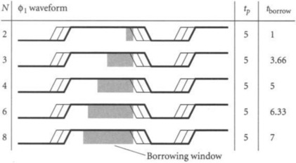
Example 3.2 illustrates the amount of time available for borrowing in an aggressive microprocessor.
EXAMPLE 3.2
Consider the microprocessor of Example 3.1 with a cycle time Tc = 16 and precharge time of tprech = 4 FO4 inverter delays. Further assume the global skew budget is 2, the local skew budget is 1, and the hold time is 0 FO4 delays. How much time can be borrowed as a function of the number of clock phases?
SOLUTION
Figure 3.4 illustrates the clock waveforms, precharge period, and maximum time borrowing for various numbers of clock phases. Notice that the best clock waveforms remain the same because the clock skew is fixed, but that the amount of time borrowing available increases with N. A two-phase system offers a small amount of time borrowing, which makes balancing the pipeline somewhat easier. A four-phase design offers more than a full phase of time borrowing, granting the designer tremendous flexibility. More phases offer diminishing returns. In Chapter 5, we will find that generating the four domino clocks is relatively easy. Therefore, four-phase skew-tolerant domino is a reasonable design choice, which we will use in the circuit methodology of Chapter 4.
3.1.3 Fifty-Percent Duty Cycle
Example 3.2 showed that skew-tolerant domino systems with four or more phases and reasonable bounds on clock skew may be able to borrow huge amounts of time using clock waveforms with greater than 50% duty cycle. As we will see in Chapter 5, it is possible to generate such waveforms with clock choppers, but it would be simpler to employ standard 50% duty cycle clocks, with te = tp = Tc/2.
We have seen that the key metric for skew-tolerant domino is the overlap between phases, te – Tc/N. We know that this overlap must exceed the clock skew, hold time, and time borrowing. Substituting te = Tc/2, we find
From Equation 3.7, we see that again the overlap approaches half a cycle as the number of clocks N gets large. Of course we must use more than two clock phases to obtain overlapping 50% duty cycle clocks.
Another advantage of the 50% duty cycle waveforms is that a full half-cycle is available for precharge. This may allow more time for slow precharge or may allow the designer to tolerate more skew between precharging gates, eliminating the need to place all paths through gates of a particular phase in the same local clock domain. Of course, in a system with 50% duty cycle clocks, tighter bounds on local skew do not permit greater global skew.
3.1.4 Single Gate per Phase
In the limit of using very many clock phases or very few gates per cycle, we may consider designing with exactly one gate per phase. The precharge constraint of Equation 3.1 requires that a gate must complete precharge before the next gate in the same phase begins evaluation so that old data from the previous cycle does not interfere with operation. Skew between the two gates in the same phase is subtracted from the time available for precharge. Because there is no next gate in the same phase when we use exactly one gate per phase, we can relax the constraint. The new constraints, shown in Figure 3.5, are that the domino gate must complete precharge before the gate in the next phase reenters evaluation, and that the dynamic gate A in the current phase must precharge adequately before the current phase reenters evaluation. In a system with multiple gates in a phase, both A and B must complete precharge by the earliest skewed rising edge of Φ1.
As a result of these relaxed constraints, a shorter precharge time tp may be used, permitting more global skew tolerance or time borrowing. Alternatively, for a fixed duty cycle, more time is available for precharge.
3.1.5 Min-Delay Constraints
Just as we saw in Section 2.2.4 that static circuits have hold time constraints to avoid min-delay failure, domino circuits also have constraints that data must not race through too early.1 These constraints are identical in form to those of static logic: data departing one clocked element as early as possible must not arrive at the next clocked element until ΔCD after the sampling—that is, falling—edge of the next element.
Figure 3.6 illustrates how min-delay failure could occur in skew-tolerant domino circuits by looking at the first two phases of an N-phase domino pipeline. Gate A evaluates on the rising edge of Φ1, which in this figure is skewed early. If the gate evaluates very quickly, data may arrive at gate B before the falling edge of Φ2, as indicated by the arrow. This can contaminate the previous cycle result of gate B, which should not have received the new data until after the next rising edge of Φ2.
The min-delay constraint determines a minimum, possibly negative, delay δlogic through each phase of domino logic to prevent such race-through. The data must not arrive at the next phase until a hold time after the falling edge of the previous cycle of the next phase. This falling edge nominally occurs Tc/N – tp after the rising edge of the current phase. Moreover, skew must be budgeted because the current phase might begin early relative to the next phase. In summary:
The hold time ΔCD is generally close to zero because data can safely arrive as soon as the domino gate begins precharge.
If the required δlogic is negative, the circuit is guaranteed to be safe from min-delay problems. Two-phase skew-tolerant domino has severe min-delay problems because tp < Tc/2, so the minimum logic contamination delay will certainly be positive. Four-phase skew-tolerant domino with 50% duty cycle clocks, however, can withstand a quarter cycle of clock skew before min-delay problems could possibly occur.
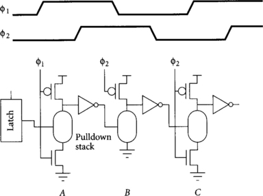
To get around the min-delay problems in two-phase skew-tolerant domino, we can introduce additional 50% duty cycle clocks at phase boundaries, as was done in Opportunistic Time-Borrowing Domino [41, 80] and shown in Figure 3.7. dlclk and dlclk_b play the roles of Φ1 and Φ2 in two-phase skew-tolerant domino, and 50% duty cycle clocks clk and clk_b are used at the beginning of each half-cycle to alleviate min-delay problems. However, this approach still requires four phases when the extra clocks are counted and does not provide as much skew tolerance or time borrowing as regular four-phase skew-tolerant domino, so it is not recommended.
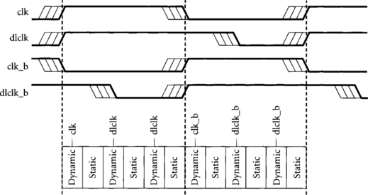
Figure 3.7 Two-phase skew-tolerant domino with additional phases for min-delay safety [41]
3.1.6 Recommendations and Design Issues
In this section, we have explored how skew tolerance, time borrowing, and min-delay vary with the duty cycle and number of phases used in skew-tolerant domino. We have found that four-phase skew-tolerant domino with 50% duty cycle clocks is an especially attractive choice for current designs because it provides reasonably good skew tolerance and time borrowing, is safer from min-delay problems than two-phase skew-tolerant domino, and, as we shall see in Chapter 5, uses a modest number of easy-to-generate clocks. Increasing the number of phases beyond four provides diminishing returns and increases complexity of clock generation. Therefore, we will focus on four-phase systems in the next chapter as we develop a methodology to mix static logic with four-phase skew-tolerant domino. Before moving on, however, it is worth mentioning a number of design issues faced when using skew-tolerant domino circuits.
The designer must properly balance logic among clock phases, just as with transparent latches where logic must be balanced across half-cycles. It is generally necessary to include at least one gate per phase because all of the timing derivations in this chapter have worked under such an assumption. When a large number of phases are employed, it is possible to have no logic in certain phases at the expense of skew tolerance and time borrowing; for example, an eight-phase system with no logic in every other phase is indistinguishable from a four-phase system with logic in every phase. The most common reason phases contain no logic is that the paths are short. These noncritical paths can introduce domino buffers to guarantee at least one gate per phase, or may be implemented with static logic and latches because the speed of domino is unnecessary.
In Section 3.1.2, we showed that if we could build each phase of logic in a local clock domain, we could shorten the precharge period tp because less skew must be budgeted between gates in the same phase. Unfortunately, in some cases critical paths and floorplanning constraints may prevent a phase of logic from being entirely within a local domain. If we do not handle such cases specially, we could not take advantage of local skew to increase tolerable global skew. Two solutions are to require that the gates at the clock domain boundary precharge more quickly or to introduce an additional phase at the clock domain crossing delayed by an amount less than Tc/N.
A final issue encountered while designing skew-tolerant domino is the interface between static and domino logic. Because nonmonotonic static logic must set up before the earliest the domino clock may rise, but the domino gate may not actually begin evaluating until the latest that its clock may rise, we have introduced a hard edge at the interface and must budget clock skew. This encourages designers to build critical paths and loops entirely in domino for maximum performance. The interface will be considered in more detail in Chapter 4.
3.2 Domino Gate Design
Now that we have analyzed skew-tolerant domino timing, let us return to general issues in domino design applicable to both skew-tolerant and traditional domino circuits. In Section 1.4.1 we saw that the monotonicity rule only allowed the use of noninverting gates in a domino pipeline. To implement arbitrary logic functions, we can employ a more general logic family, dual-rail domino. We also saw that the precharge rule required us to avoid contention between pulldown and pullup transistors during precharge. We will look at the use of footed and unfooted gates to satisfy this rule. In systems that stop the clock to dynamic gates, it is necessary to use keepers to avoid floating nodes. We will look at various issues in keeper design. Once these basic issues of monotonicity, precharge, and static operation are understood, we will address robustness issues necessary for reliable operation.
3.2.1 Monotonicity and Dual-Rail Domino
The monotonicity rule says that dynamic gates should have monotonically rising inputs during evaluation; that is, the inputs should start low and stay low, start high and stay high, or start low and rise, but never start high and fall because the dynamic gate will never be able to recover from a false evaluation. Because the output of a dynamic gate is monotonically falling, it must be followed by an inverting static gate to create a monotonically rising input to the next dynamic gate. The domino gate, consisting of the dynamic/static pair, therefore always performs two inversions and thus can only implement noninverting functions. Such functions are called monotonic; they include AND and OR, but not XOR.
In traditional domino circuits, a common solution to the monotonicity problem is to structure a block of logic into a first monotonic portion followed by a second nonmonotonic portion. The first portion is implemented with domino logic, while the second portion is built with static CMOS gates. The result goes to a latch at the end of the half-cycle, and domino logic may begin again at the start of the next half-cycle. For example, a 64-bit tree adder consists of a carry generation tree followed by a final add. The carry generation to compute the carry in to each bit is monotonic, but the final add requires the nonmonotonic XOR function. Therefore, some designs perform the add in a half-cycle by building the carry logic with domino and the XOR with static CMOS at the end of the half-cycle [49]. This approach has three drawbacks. One is that mixing domino and static CMOS is not as fast as using domino everywhere. Another is that it requires traditional domino clocking techniques and thus has severe sequencing overhead. A third is that the adder is forced to fit in half of a cycle so that the nonmonotonic output arrives at the first half-cycle latch. This may limit the cycle time of the machine.
An alternative solution to monotonicity is to construct dual-rail domino circuits, also known as dynamic differential cascade voltage switch logic (DCVS) [35]. Dual-rail domino circuits accept both true and complementary versions of the inputs and produce true and complementary outputs. For example, Figure 3.8 shows a dual-rail domino AND/NAND gate, and Figure 3.9 shows an XOR/XNOR gate.
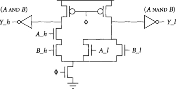
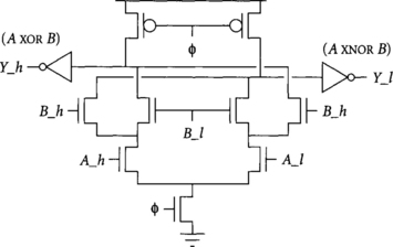
The true and complementary signals are labeled _h and _l, respectively. When a dual-rail domino gate precharges, both _h and _l outputs are low, representing a quiescent state. When the gate evaluates, either _h or _l will rise, indicating that the function is TRUE or FALSE, respectively. The gate should never assert both _h and _l outputs high simultaneously; this state would indicate erroneous operation of the gate.
Dual-rail domino gate design is much like single-rail design, but requires building pulldown stacks implementing both true and complementary versions of the function. For some functions, these stacks are completely independents; for example, in Figure 3.8 the AND function is a regular domino AND gate using true versions of the inputs, while the NAND function is a domino OR gate operating on complementary inputs. For other functions, the stacks may be partially shared as illustrated in Figure 3.9. Sharing reduces the input capacitance and thus generally improves speed as well as area. Sharing can be determined by inspection or by Karnaugh maps or tabular methods [12].
Dual-rail domino gates require dual-rail inputs. The gates producing these inputs must in turn receive dual-rail inputs. This means that entire blocks of logic must be implemented in dual-rail fashion. For example, the 64-bit tree adder discussed earlier can be built entirely from dual-rail domino. This improves performance by hiding the sequencing overhead and avoiding the use of a slow static XOR, leading to a speedup of 25% or more in aggressive systems [30]. The improvement comes at the expense of twice as many wires to carry the dual-rail signals and greater clock loading serving the dual-rail gates.
Dual-rail domino design is otherwise very similar to regular domino design. In the next sections, discussions of footed and unfooted gates, keepers, and noise margins apply equally to regular domino and dual-rail domino logic.
3.2.2 Footed and Unfooted Gates
The precharge rule of domino gates states that there must be no active path from the output to ground in a domino gate during precharge. Otherwise, the gate would dissipate excess power and the output would not precharge adequately. This rule can be enforced in two ways: an explicit transistor can be used to cut off the path to ground, or the circuit can be timed such that paths to ground are deactivated before precharge begins. Footed gates use the extra transistor, while unfooted gates can be faster; these styles were shown in Figure 1.10.
Footed gates are safe to use anywhere, but unfooted gates require that all paths to ground be deactivated before the gate begins precharge. One way to guarantee this is to use inputs coming from other domino gates and to delay the precharge until the inputs have had time to precharge. For example, Figure 3.10 illustrates proper use of footed and unfooted gates. Dynamic gate A receives inputs from a static latch. The oval represents a pulldown stack of NMOS transistors implementing an arbitrary function. Because that latch output might be high during precharge, the gate needs a series evaluation transistor to avoid contention during precharge. Dynamic gate B begins precharge on the falling edge of Φ2 and receives inputs from a dynamic gate A that precharges on the falling edge of Φ1· Hence, the input will be low by the time gate B begins precharge, so no evaluation transistor is required. Gate C begins precharge at the same time as B, so its inputs are not low until partway through the precharge period. Therefore, gate C should use an evaluation transistor to avoid contention. In summary, an unfooted gate may be used when its inputs come from a domino gate that begins precharge earlier.
Note that only one transistor in each series stack must be off during precharge to avoid contention. For example, an unfooted dynamic NAND can receive some inputs from static latches so long as at least one input came from a previous phase of dynamic logic. On the other hand, an unfooted dynamic NOR gate must have all inputs low during precharge to avoid contention.
To avoid contention in an unfooted gate completely, the gate must not begin precharge until the previous gate has had enough time to fully precharge. Guaranteeing this across process and environmental variations is difficult and makes unfooted gates hard to use. However, if the gate begins precharge while its inputs are falling but not completely low, contention will only occur for a short time. This may be acceptable in some design methodologies that sacrifice power to achieve maximum speed.
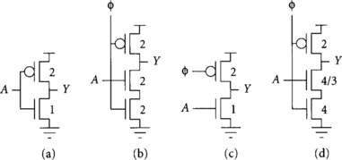
The method of logical effort [79] can be used to estimate the advantage of unfooted gates. Recall that the logical effort of a gate is the ratio of its input capacitance to that of a static CMOS inverter that can deliver the same output current. The logical effort indicates how good the gate is at driving a capacitive load; lower logical efforts correspond to faster gates. Figure 3.11 compares three dynamic inverters sized for equal output current as a static CMOS inverter. The static CMOS inverter (a) presents three units of capacitance to the A input, as indicated by the bold transistor widths. Footed dynamic inverter (b) has two units of input capacitance on the data input, meaning the logical effort is 2/3. Unfooted dynamic inverter (c) has one unit of input capacitance, meaning the logical effort is only 1/3. Footed dynamic inverter (d) uses a larger clocked evaluation transistor to allow a smaller data input transistor, achieving a logical effort of 4/9. In summary, unfooted dynamic gates have the lowest logical effort. Footed dynamic gates can approach the logical effort of unfooted gates at the expense of larger clocked transistors. Although these transistors do not load the critical path, they do increase clock loading, which increases power consumption and, indirectly, clock skew.
3.2.3 Keeper Design
The dynamic gates we have shown so far have a minimum operating frequency because the output may float high while the gate is in evaluation. If left floating too long, the charge may leak away. Just as latches can be made static by placing a cross-coupled inverter pair on the storage node, dynamic gates can use a keeper, also called a sustainer, to prevent the floating node from drifting. We will see later that keepers also significantly improve the noise margin of dynamic inputs.
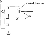
Figure 3.12 shows a keeper on a domino gate. The keeper is a weak PMOS transistor driven by the output inverter. When the dynamic output X stays high during evaluation, the keeper supplies a trickle of current to compensate for any leakage. When X pulls low during evaluation, the keeper turns off to avoid contention.
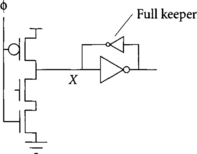
The first dynamic gate in a phase of skew-tolerant domino may float either high or low when the clock is stopped because the precharge transistor is turned off and the inputs fall low when the previous phase precharges. Therefore, such gates may require a full keeper built from a pair of cross-coupled inverters, as shown in Figure 3.13.
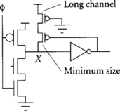
Keepers should be small to minimize loading on the forward path and to avoid fighting the dynamic gate while it switches. For small dynamic gates, even minimum-sized keepers are too strong. In such a case, the channel length may be increased. Unfortunately, simply increasing the length increases the capacitive load on the critical path and thus slows the circuit. An alternative implementation of a very weak keeper is shown in Figure 3.14. The output feeds back to a minimum-size keeper. In series with the keeper is an extra transistor of minimum width and longer than minimum length that acts to reduce the current delivered by the keeper.
3.2.4 Robustness Issues
Static CMOS gates are very robust; given sufficient time, they always settle to the correct result. Domino gates are more sensitive to noise and can be irrecoverably corrupted if exposed to noise. Therefore, an essential part of domino design is a good understanding and verification of noise problems. This section surveys the noise sensitivity of dynamic inputs and outputs, then examines several sources of noise in domino circuits: charge sharing, capacitive coupling, power supply noise, alpha particles, and minority carrier injection.
Both the input and output of dynamic gates are sensitive to noise, but the mechanisms differ. In Figure 3.15, node X is the output of a dynamic gate and the input of a hi-skew static gate. It is precharged high, then may float high during evaluation. Because it is floating rather than actively driven, it is especially sensitive to noise that might cause it to fall. Moreover, the hi-skew inverter is sized to respond quickly to a falling transition on x. Therefore, its switching threshold is likely closer to 2/3 VDD than 1/2 VDD, leaving a smaller noise margin. Node Y is the input to the next dynamic gate and output of the HI-skew inverter. It is less prone to noise because it is actively driven by the inverter. However, the noise margin of the dynamic input is only a threshold voltage Vt before the NMOS transistor begins to conduct and improperly discharge the dynamic gate.
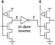
In summary, dynamic outputs are especially noise-prone, but go to receivers with medium noise margins. Dynamic inputs are less noise-prone, but go to receivers with tiny noise margins. In the remainder of this section, we will explore the sources of noise that may impact the dynamic inputs and outputs.
Charge Sharing
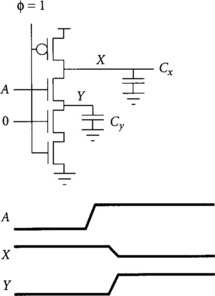
Charge sharing occurs on a dynamic output when a transistor turns on and transfers charge between two floating capacitors. For example, consider the dynamic NAND gate in Figure 3.16. The capacitor Cy on the internal node represents parasitic diffusion capacitance, while the capacitor Cx on the output represents both diffusion capacitance and the output load. Initially, suppose the gate is in evaluation, the output X is precharged to VDD, but that internal node Y was discharged to GND. When the top NMOS transistor turns on, the output is not logically supposed to change because the other NAND input is low. However, charge redistributes between Cx and Cy until the voltages equalize.2 This charge sharing causes the output to droop while the internal node rises. If the output droops too far, an incorrect value is produced. The final voltage on the output is set by the capacitive voltage divider equation:
Charge sharing is minimized by making the internal diffusion capacitances small compared to the load capacitance. The diffusion capacitance depends on layout, so it is important to carefully lay out dynamic gates. Driving larger load capacitances also reduces charge sharing, but of course increasing the load excessively slows the dynamic gate.
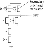
Even after careful layout, charge sharing is often unacceptably great in complex domino gates with many internal nodes. In such a case, charge sharing can be alleviated by precharging internal nodes with a secondary precharge transistor, as shown for a complex AND-OR-INVERT (AOI) gate in Figure 3.17. Each precharge device adds extra diffusion capacitance that slightly slows the gate, so it is best to only precharge the smallest number of internal nodes necessary to satisfy noise margins. A guideline is that precharging every other node is generally sufficient to keep charge-sharing noise to about 10% of the supply voltage for most gates. Be careful of contention if precharging internal nodes in unfooted dynamic gates.
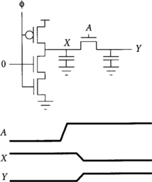
A related form of charge sharing occurs when dynamic gates drive pass transistors, as shown in Figure 3.18. When the pass transistor turns on, charge is shared between the dynamic node X and the pass transistor output Y. Therefore, dynamic gates should not drive the source/drain inputs of pass transistors.
Capacitive Coupling
Capacitive coupling, also known as crosstalk, is a major component of noise on both inputs and outputs of dynamic gates. Wires adjacent to a domino gate may have capacitance to the dynamic gate input or output. The adjacent wire is called the aggressor or perpetrator, while the dynamic input or output is the victim. When the aggressor switches, it tends to drag the victim along, injecting noise onto the victim. Floating dynamic outputs are especially susceptible to coupling. Dynamic inputs must also be checked because of their tiny noise margin, but receive less coupling because they are actively driven and the driver fights against the coupling.
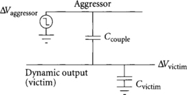
The coupling onto a dynamic output is modeled in Figure 3.19. The victim has Ccouple coupling capacitance to the aggressor and Cvictim capacitance to other nodes such as the substrate that are not switching. When the aggressor line falls, the victim line will tend to fall too. As with charge sharing, we have a simple capacitive voltage divider, so the noise ΔVvictim on the victim is
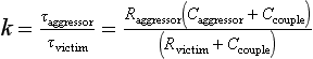
The coupling onto a dynamic input is modeled in Figure 3.20. The victim is sensitive to a rising aggressor, which could drag the victim high enough to turn on the dynamic gate. This time, the resistance of the aggressor and victim drivers is important. This resistance can be computed from the linear I-V characteristics of the driver transistor. If the victim has a very strong—that is, low-resistance—driver, it will be virtually immune to coupling because its driver will keep the victim low. The time constant ratio k of the aggressor to victim determines how fast the victim can respond relative to the rate at which the aggressor injects noise [91]:
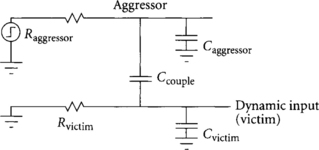
where the time constant ratio is
Coupling is an increasing problem as the height-to-separation ratio of wires increases in finer geometry processes, increasing the ratio of Ccouple to other capacitances. For example, even in a 0.8-micron process, over 50% of the capacitance of a minimum pitch metal 2 wire is to adjacent lines. It is important not to be overly pessimistic about coupling lest design of domino logic become impossible. For example, we can take advantage of the fact that a victim is only sensitive to noise while in evaluation to avoid factoring in coupling noise from aggressors that switch in a different phase.
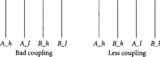
Coupling problems can be reduced by increasing the spacing between the aggressor and victim or by shielding the victim with narrow ground lines. In dual-rail domino, proper routing can also reduce coupling problems, as illustrated in Figure 3.21. If signals are routed as shown on the left, a victim may be susceptible to aggressors on both sides. If the signals are interdigitated as shown on the right, the victim will never see more than one aggressor switching at a time because either the _h or _l rail, but not both, will switch. Other approaches to coupling noise reduction include recoding busses as one-hot for fewer transitions [34] and inserting extra static inverters at the beginning and end of long lines to filter noise [62].
Power Supply Noise
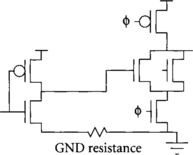
Another source of noise in dynamic gates comes from power supply variation across the die. Suppose a static inverter drives a dynamic input and that the ground potential of the inverter is higher than that at the dynamic gate due to IR drops across the ground network, as shown in Figure 3.22. If the ground difference exceeds Vt, the dynamic gate will turn on and incorrectly evaluate. Of course, power supply noise impacts dynamic outputs as well, though the noise margins are greater.
Power supply noise is especially insidious because of the trends toward lower voltage and higher power. Higher power increases the supply curquadratically. rent. Lower voltage also increases the supply current if power were held constant. Hence, the current is increasing For a fixed current, the IR drop through a power supply wire increases as a fraction of the supply voltage when voltages drop. Therefore, power supply noise as a fraction of the supply voltage is getting worse cubically if supply resistance does not change! To combat this, designers are dedicating increasing amounts of metal to the power supply network to reduce the resistance. Some chips place solder bumps carrying power and ground approximately every millimeter over the surface of the die to minimize the length and resistance of supply lines. The DEC Alpha 21264 lacked such solder bump technology so instead dedicated entire planes of metal to VDD and GND [22] in much the same way as multilayer printed circuit boards use power and ground planes. The amount of supply noise is a trade-off between cost and performance. Typically enough metal resources are dedicated to the supply to keep IR drops down to 10% across the chip [52].
Another source of power supply noise is di/dt noise from changing supply current. Power supply pins have inductance and thus higher impedance at high frequencies; they cannot supply all of the instantaneous current required by gates. Instead, this current is drawn from on-chip bypass capacitance. Idle gates present substantial bypass capacitance, but high-speed designs often must add extra explicit bypass capacitors in empty parts of the chip, especially near large clock drivers. The greatest supply noise occurs when the clock switches. Therefore, multiphase domino clocking reduces peak noise by spreading the current spikes across the cycle.
Alpha Particles
Alpha particles are helium nuclei (two protons and two neutrons) emitted from radioactive decay. They occasionally crash into chips and leave a trail of electron-hole pairs in the silicon substrate [40]. These carriers may be collected onto floating nodes, disturbing the voltage of dynamic outputs. Such disturbances are called soft errors. To minimize this change, the energy held on the capacitance of the floating node must be much greater than the energy in the alpha particle. Typical design rules call for a minimum of several femtofarads of capacitance on any dynamic node [66]. Therefore, alpha particle hits are only a problem for very small dynamic gates and SRAMs.
Interestingly, lead solder is a common source of alpha particles. Chips that use C4 solder bump packing technology may have hundreds of lead solder bumps covering the die. Placing memory arrays and sensitive dynamic gates under these bumps may be hazardous! It is rumored that some companies have cornered the market on Roman lead, which has naturally decayed and thus has lower alpha particle emissions!
Minority Carrier Injection
Certain circuits such as I/O drivers powering inductive loads are prone to ringing, which may send the output below GND. In such a case, the drain-substrate junction becomes forward biased and injects charge into the substrate. This charge may be collected on nearby dynamic nodes, corrupting the value. To prevent this, circuits prone to charge injection should be placed far away from dynamic logic. They should also be surrounded by guard rings [26]. Charge injection is only a concern with special-purpose circuits and therefore is not part of the noise budget of most dynamic gates.
Noise Feedthrough
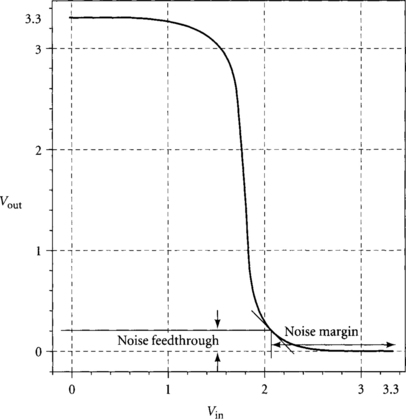
When the input of a gate is near its noise margin, the output voltage will not be at the rail. Therefore, the input of the next gate will see some noise; this is called noise feedthrough or residual noise. Indeed, the noise margin of a gate is defined by this feedthrough: it is the point at which the noise slope of the transfer function is −1 so that the marginal increase in noise feedthrough to the next gate equals the marginal increase in noise margin of the current gate.
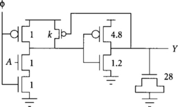
Figure 3.23 shows the transfer function of a hi-skew inverter using a PMOS transistor four times as large as the NMOS transistor. Because we are using the inverter after a dynamic gate, we are concerned about the high input noise margin, the amount the dynamic output can droop before the hi-skew inverter no longer produces a valid 0. This is determined by the unity-gain point marked on the transfer curve. Notice that at this point, the output is not quite zero. The nonzero voltage shows up as noise at the sensitive input of the next dynamic gate. In this case, the noise margin is 1.22 volts (37% of the supply) and the noise feedthrough is 0.23 volts (7% of the supply).
Summary of the Noise Budget
We have seen that domino logic is subject to numerous sources of noise. Dynamic outputs are especially noise-prone, but drive static gates with reasonably good noise margins. Dynamic inputs experience less noise, but have a noise margin of only about Vt. Most noise sources scale with the power supply voltage, so noise budgets expressed as a fraction of the supply voltage tend not to change very much with feature size and supply voltage. In this section, we will create some sample noise budgets and see that each source of noise must be tightly bounded.
For the sake of concreteness, let us develop our budget using the Hewlett-Packard CMOS14 0.6-micron 3.3v process. As we saw in Figure 3.23, the dynamic output drives a hi-skew static inverter with a noise margin of 37% of the supply voltage, causing a noise feedthrough of 7%. We assume the dynamic gate has a small keeper and thus achieves a noise margin of 19% with a feedthrough of 5%. These noise margins are measured in the worst-case process corners: SF for the hi-skew inverter and FS for the dynamic input.
Table 3.1 shows a sample noise budget for dynamic inputs and outputs. It assumes that dynamic inputs and outputs are kept within local blocks and therefore see less power supply noise than is found across the entire die.
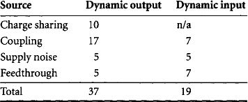
The sample budget shows that very little coupling noise can be tolerated. This can make domino design costly because signals must be shielded or widely spaced to avoid coupling. However, most circuits do not experience the worst case of all noise sources simultaneously. For example, dynamic NOR gates are not susceptible to charge sharing. Therefore, a less pessimistic noise verification tool can check each circuit individually to allow greater coupling noise on nodes that experience less of other noise sources. Moreover, dynamic logic is sensitive to the duration as well as the magnitude of noise; for example, larger peak coupling noise could be permitted if the peak coupling occurred for only a fraction of a gate delay [51].
Similarly, the minimum noise margins for dynamic outputs and inputs are determined by different process corners. For example, when the dynamic input is at its minimum noise margin in its least favorable process corner and produces the most feedthrough noise, the dynamic output will be in its most favorable corner and will be able to tolerate more noise, somewhat alleviating the feedthrough noise problem.
A common mistake is to ignore the other sources of noise when focusing on a particular problem. For example, a designer may simulate charge sharing and conclude that no secondary precharge transistor is necessary because charge sharing that causes a 30% output voltage droop on a dynamic gate does not trip the subsequent static inverter in simulation. Of course, when other sources of noise such as coupling and supply noise are introduced, the circuit will fail.
Domino logic allows a trade-off between noise margins and performance. If the dynamic output has inadequate noise margin, it can be improved by using a lower-skew static gate; however, the gate will not respond as quickly to falling transitions, so the circuit will be slower. If the dynamic input has inadequate noise margin, it can be improved by using a bigger keeper. The keeper is especially effective because it is fully on while the NMOS pulldown transistor is just barely on when the dynamic input voltage is slightly above Vt. For example, the keeper in the sample noise budget was 1/5 the size of the input transistor. Doubling the keeper size increases the dynamic input noise margin from 19% to 27% of the supply voltage. The keeper also slightly improves the noise margin of the dynamic output. However, increasing the keeper size slows the falling transition of the dynamic output because of contention and increased loading.
3.3 Historical Perspective
The motivation for using dynamic logic has changed strikingly over the past two decades. In the NMOS days of the 1970s, dynamic logic was used to reduce power consumption inherent in NMOS logic [60, 65] and to save area on precharged busses [56]. Domino logic was proposed for CMOS as “high-speed compact” logic [49]. The risks associated with the tight domino noise margins deterred use in commercial products. Moreover, critical paths could often be solved by using more parallel, area-intensive circuits; for example, a designer could choose a static CMOS carry look-ahead adder instead of using domino logic for a ripple carry adder.
The relative importance of area, power, and speed shifted by the early 1990s. Area, once the primary limitation of CMOS circuit design, becomes cheaper with each generation of process. The trends toward shorter cycles that we observed in Section 1.2 have pushed logic to use the fastest, most parallel algorithms available because area is so inexpensive. To achieve even shorter cycle times as measured in gate delays, processors had to employ dynamic logic. For example, designers of the HP-PA8000 microprocessor found that extensive use of dynamic logic (40% of the gates were dynamic) was a key factor in achieving desired performance [20, 21]. Power consumption and area ceased to be motivations for using dynamic gates. Indeed, the power consumption of domino logic is much higher than static logic because power in logic circuits is dominated by switching the clock capacitance [25]. Trends toward more dual-rail domino actually increase circuit area as well!
A key requirement for using domino logic is the thorough understanding and checking of noise budgets. DEC has a particularly well-established and documented domino circuit methodology [26]. Remarkably, DEC did not use keepers on dynamic gates in the 21164, despite the fact that threshold voltages were an aggressively low 0.35v! However, keepers ultimately became necessary in the 21264 to offset NMOS leakage current [3]. The use of domino has mostly been restricted to custom, highly optimized chips such as microprocessors because guaranteeing signal integrity is beyond the capability of current turnkey synthesis and place-and-route tools used by most ASIC designers. IBM’s static noise analysis tool [76] is an interesting approach to the problem of automatic noise analysis.
As cycle times measured in gate delays have decreased, the sequencing overhead of domino logic has become a greater problem. Williams observed that latches were unnecessary between blocks of domino logic so long as one block could evaluate before the next began precharge. He used this observation to construct “zero-overhead” asynchronous circuits [93, 94]. Synchronous designers began to adopt the ideas of skew-tolerant domino by the mid-1990s. Hewlett-Packard used a “pipeline latch” in the PA7100 floating-point multiply-accumulate (FMAC) path to soften the clock edges and reduce the impact of clock skew [33]. Intel used “Opportunistic Time-Borrowing (OTB) Domino” on the Itanium Processor. OTB is a variant of two-phase skew-tolerant domino coinvented by this author [41, 80]. Another Intel team has made an extensive effort to develop self-resetting domino [11], an interesting and important technique that is beyond the scope of this book. DEC used overlapping clocks to eliminate latches between domino blocks in the ALU and select other paths of the Alpha 21164 [6]. Sun also used a similar technique, which they called “delayed reset domino,” in the UltraSparc [53]. Most microprocessor companies, including Advanced Micro Devices, Silicon Graphics, Motorola, Hewlett-Packard, Sun Microsystems, and IBM, have developed the ideas of skew-tolerant domino, though have generally kept their use as a trade secret.
3.4 Summary
Domino gates have become very popular because they are the only proven and widely applicable circuit family that offers significant speedup over static CMOS in commercial designs, providing a 1.5 to 2 times advantage in raw gate delay. However, speed is determined not just by the raw delay of gates, but by the overall performance of the system. For example, traditional domino sacrificed much of the speed of gates to higher sequencing overhead. As cycle times continue to shrink, the sequencing overhead of traditional domino circuits increases and skew-tolerant domino techniques become more important. Skew-tolerant domino uses overlapping clocks to eliminate latches and remove the three sources of sequencing overhead that plague traditional domino: clock skew, latch delay, and unbalanced logic. The overlap between clock phases determines the sum of the skew tolerance and time borrowing. Systems with better bounds on clock skew can therefore perform more time borrowing to balance logic between pipeline stages. Increasing the number of clock phases increases the overlap, but also increases the complexity of local clock generation and distribution. Four-phase skew-tolerant domino, using four 50% duty cycle clocks in quadrature, is a particularly interesting design point because it provides a quarter cycle of overlap while minimizing the complexity of clock generation.
Domino gates are very susceptible to noise. Dynamic inputs have a very low noise margin and are especially impacted by coupling and power supply noise. Dynamic outputs have a larger noise margin, but are impacted by charge sharing as well. Domino gates should be checked for the following electrical rules:
![]() Neither inputs nor outputs of dynamic gates should connect to diffusion terminals of pass transistors.
Neither inputs nor outputs of dynamic gates should connect to diffusion terminals of pass transistors.
![]() Nodes that may float indefinitely must be held by keepers.
Nodes that may float indefinitely must be held by keepers.
![]() Coupling onto dynamic inputs and outputs must be limited.
Coupling onto dynamic inputs and outputs must be limited.
![]() Noise margins on dynamic inputs and outputs must be checked.
Noise margins on dynamic inputs and outputs must be checked.
The next chapter will further explore the use of skew-tolerant domino in the context of an entire system, describing a methodology compatible with other circuit techniques but that still maintains low sequencing overhead.
3.5 Exercises
[15] 3.1. Sketch a diagram like Figure 3.1 illustrating a six-phase domino pipeline with 50% duty cycle clocks and one domino gate per clock phase. Indicate clock skew of one-sixth of the cycle.
[15] 3.2. A domino gate has an evaluation time of 100 ps and a precharge time of 200 ps. If there is 50 ps of skew between the clock controlling the gate and its successors in the same phase, what is the minimum time tpthat the clock must be low?
[20] 3.3. Repeat Example 3.1 if the cycle time is 12 FO4 delays and the precharge time is 3 FO4 delays.
[20] 3.4. Repeat Example 3.2 if the cycle time is 12 FO4 delays and the precharge time is 3 FO4 delays.
[15] 3.5. A four-phase skew-tolerant domino pipeline runs at 800 MHz in a 0.18-micron process with a 60 ps FO4 delay. You can adjust the duty cycle of the clocks for best performance. If you allow a precharge time of 5 FO4 delays and a hold time of 1 FO4 delay, when there is 50 ps of local clock skew, how much global skew can you tolerate? If the actual global skew is 200 ps, how much time borrowing can you permit?
[30] 3.6. Repeat Exercise 3.5 if you design to guarantee exactly one domino gate per clock phase.
[20] 3.7. A four-phase skew-tolerant domino pipeline runs at 1.25 GHz using 50% duty cycle clocks. The required overlap between phases is thold = −15 ps. Each domino gate has a contamination delay of 35 ps and a hold time ΔCD of −10 ps. How much clock skew can the pipeline withstand before one gate might precharge before its successor could consume the result? How much clock skew can the pipeline withstand before min-delay problems might occur? In summary, how much clock skew can the system withstand?
[20] 3.8. Sketch transistor-level implementations of the following footed dual-rail dynamic gates:
[20] 3.9. Sketch transistor-level implementations of the following footed dynamic gates. Label each NMOS transistor with the appropriate width to provide the same output drive as a unit inverter (see Figure 3.11). Select the PMOS transistor width for half the output drive as the pulldown stack. Estimate the logical effort of each data input to the gate.
[15] 3.10. Repeat Exercise 3.9 for unfooted dynamic gates.
[30] 3.11. Make plots of evaluation time and precharge time for the domino buffer in Figure 3.24 as a function of the precharge transistor size P. The transistor and load sizes have been selected to provide a stage effort of about 4. Use step inputs. Measure evaluation time to 50% output of the static inverter when Φ is already high and A rises. Measure precharge time from the falling edge of Φ to the static inverter output Y dropping to 10% of VDD. Use your favorite process, environment, and SPICE simulator. Let the dimensions be in units of 10 microns of gate width. What value of P would you select for general application?
[30] 3.12. Make plots of evaluation time and input noise margin for the domino buffer in Figure 3.25 as a function of the keeper transistor size k. Use step inputs. Measure evaluation time to 50% output of the static inverter when Φ is already high and A rises. Measure noise margin at the unity gain point of the output Y. Use your favorite process, environment, and SPICE simulator. Let the dimensions be in units of 10 microns of gate width. What value of k would you select for general application?
[30] 3.13. Design a dynamic footed AOAOAOI gate to compute B(C + D(E + F(G + H))). Choose the transistor sizes to have a maximum of 20 microns of gate width on any input. The gate should drive an inverter with a total of 20h microns of gate width. Simulate it in SPICE, being sure to include AS, AD, PS, and PD parameters to specify diffusion parasitics. Find the worst-case charge-sharing noise on the output for h = 0, 1, 2, 4, and 8. How does the noise depend on h? Why? Add secondary precharge transistors to precharge every other internal node. Repeat your charge-sharing measurements. Explain your observations.
[30] 3.14. Simulate capacitive coupling between two metal lines. Each line has a capacitance to ground of 0.1 fF/micron and a capacitance to the adjacent line of 0.2 fF/micron. The aggressor’s driver is a falling voltage step with an effective resistance of 100 Ω. The victim is a dynamic node; the keeper has an effective resistance of R. Plot the peak coupling noise versus R for 100-micron and 1 mm line lengths. How do your results compare with the predictions of Equation 3.11?
[25] 3.15. Simulate the DC transfer characteristics of an inverter in your process, using a P/N ratio of 2. Find the unity gain points on the transfer function. Measure Vin–l and Vin–h, the input voltages at the low and high unity gain points; and Vout–l and Vout–h, the output voltages at these points. What are the high and low noise margins for your inverter?
[25] 3.16. Repeat the simulation of Exercise 3.15 with a P/N ratio of γ. What value of γ gives equal high and low noise margins in your process?
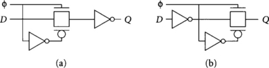
[25] 3.17. Identify potential noise problems in the circuit in Figure 3.26. Draw an improved circuit with reduced noise risk.
[15] 3.18. An early stepping of a well-known microprocessor suffered unreliable operation due to noise. The problem was traced to a path between two widely separated units. The receiving unit used a transmission-gate latch, as shown in Figure 3.27(a). The problem could be fixed by substituting a different transparent latch, shown in Figure 3.27(b). Explain why the noise problem might occur and how the input noise margins of each latch compare.