1 Powering Microsystems with Ambient Energy
CONTENTS
1.1.2 Energy and Power Requirements
1.3 Conditioning Microelectronics
1.4 Energy-Harvesting Chargers and Power Supplies
1.4.1 Battery-Assisted Photovoltaic Charger–Supply Example
1.4.2 Piezoelectric Charger Example
1.4.3 Electrostatic Charger Example
Abstract: The demand for portable, lightweight, and long-lasting electronics is relentless, filling a growing need in the military to lighten and extend reconnaissance mission work; in space exploration for remote sensors; in biomedical applications for monitoring, prognosis, treatment, and others; and in consumer electronics for disposable and rechargeable everyday products. Conforming to microscale dimensions means that energy and power supplies, conditioning and processing microelectronics, sensors, wireless transceivers, and other constituent subsystems must synergistically share a common miniaturized platform. Integrating and managing microsources, however, present a myriad of diverse and interdependent mechanical, chemical, and electrical challenges. One pivotal constraint is that ultrasmall systems cannot store the energy required to sustain practical lifetimes, which is why energy harvesters have gained so much attention. This chapter aims to illustrate how to energize and power microsystems from ambient energy by reviewing system requirements, describing the state of the art in miniaturized energy-harnessing transducers, and presenting energy-harvesting supply and charger microelectronics currently under investigation and development.
1.1 Microsystems
Considering today’s growing demand for and operational needs of portable microelectronics is critical in drafting a strategy for supplying a derivative application space that is barely emerging, like wireless microsensors. The challenge is to understand today’s market and needs well enough to predict the challenges society will face at the time that research reaches a commercialization stage. Equally important is comprehending not only the state-of-the-art of technologies needed to build such systems, but also the trends that drive them so that today’s efforts can have a chance at leveraging the future benefits of technologies currently under development. Ultimately, though, predictions of this sort, however good they may be, amount to speculation that scientists and engineers must continually fine-tune over time and with experience.
1.1.1 Market Demand
Consumers continue to enjoy and, in consequence, demand smaller and more functionally dense products. Unfortunately, tiny devices necessarily constrain sources to small spaces, limiting the amount of energy they store and how much power they supply to impractically low levels. Consider, to cite an illustrative example, that 100 μW, which is drastically below what wireless telemetry requires today to transmit over a distance of 100 m, completely discharges a 5 × 3.8 × 0.037-cm3 1 mA·Hr thin-film lithium ion battery (Li ion) in 10 h. Adding functionality, as in the case of cellular phones and the applications they now support, only exacerbates the issue because the extra power overhead drains a source that is already easily exhaustible even faster. Although today’s efforts aim at reducing the energy that each additional function requires, the cumulative load that wireless transmission and several low-power functions present to a miniature source is nonetheless substantial, reducing the operational life of the system considerably, to the point at which consumers lose interest.
Perhaps a more significant application space emerges in the wake of integration in the form of in situ but nonintrusive devices, such as biomedical implants. While the motivation for and benefits of monitoring biological activity with in vivo contraptions without frequently replacing or recharging batteries are for the most part obvious, the commercial and societal advantages of retrofitting low-overhead, noninvasive intelligence into expensive and difficult-to-replace technologies like the power grid are arguably more economically, sociologically, and ecologically profound. Feeding performance metrics and the use of energy in a factory into a central processor, for instance, to determine the optimal use of power cannot only save energy on a grander scale when applied across a wide region, but also reduce the emission of environmentally harmful by-products and the need for politically charged petroleum. From a commercial standpoint, the potential ubiquity for such miniature sensors across factories, hospitals, airports, farms, homes, subway stations, shopping malls, and other such centers rivals and quite likely exceeds that of cellular phones at maybe 10 to 100 sensors for every 10 × 10 m2 of surface area.
1.1.2 Energy and Power Requirements
Modern microelectronic systems necessarily embed both analog and digital functions—analog because they must not only manage and process continuous real-life signals (e.g., seismic activity, sound waves, motion, temperature, pressure, and others) but also draw energy and condition power from nonideal sources. State of-the-art applications, however, also include digital blocks because binary processes enjoy considerably higher noise margins, which is another way of saying they exhibit higher signal-to-noise ratios (SNRs). The fact is that a small voltage variation, say, from 20 to 400 mV, across a 0–1.8 V digital signal has little to no impact on the output word and its bit-error rate (BER), whereas the same variation in a rail-to-rail analog signal swing essentially eradicates more than 1% to 22% of the data. All this is to say the system draws quiescent and switching power from the source, as Figure 1.1 shows [1].
Because the going trend is to incorporate more functionality into a product, a fixed supply voltage is no longer optimal, especially when seeking to extend operational life. While digital-signal processors (DSPs), for example, may draw milliwatts at 1 V, voltage-controlled oscillators (VCOs) and analog–digital converters (ADCs) can demand considerably less power at maybe 1.8 V and power amplifiers (PAs) significantly more power at 3 V. The end result is a system that, to operate optimally, includes multiple supply voltages capable of feeding diverse power levels.

FIGURE 1.1 General loading profile that a modern microsystem presents to a source over time.
In the end, irrespective of the supply voltages needed, featuring multiple tasks ultimately burdens a source with additional loads. The problem with a miniature source is that energy is scarce and power levels are low. One way of reducing power in the system is to duty-cycle or time-division multiplex tasks across time so that no more than one set of interdependent functions operates at any given point. Similarly, powering blocks only when absolutely necessary, as in on-demand, reduces energy that the system would otherwise waste. As a result, systems today dynamically change operating modes on the fly, as Figure 1.1 illustrates, where all average and peak power, pulse width, and switching frequency change according to the tasks performed.

FIGURE 1.2 Probability-density curve for radio-frequency (RF) power amplifiers (PAs) in CDMA (code division multiple access) handset applications.
Extending the operational life of smart microsensors remains a challenge, even after power-moding and duty-cycling functions. The point is that marketable micro-systems must draw little to no power. Luckily, portable and sensor applications naturally call for low duty-cycle operation because devices need not function continuously. The cellular phone, for instance, is for the most part alert—that is, ready to receive calls—and while transmission demands milliwatts, awareness only requires microwatts, which is why radio-frequency (RF) power amplifiers are mostly in the light-to-moderate power region of operation, as Figure 1.2 demonstrates [2]. Said differently, while talking continuously on the phone for 3 to 5 hours exhausts a fully charged battery, idling might do so in 5 to 7 days.
While energy and power unavoidably relate, meeting the energy requirements of a microsystem does not necessarily imply the source can also supply the power needed. This means that reducing losses to save energy, for example, by shutting off unused circuit blocks, is as important as duty-cycling tasks over time to decrease power. The source and the circuits that manage the source must therefore account for and respond to various mixed-signal modes whose average and peak power levels, pulse widths, rise and fall times, and switching frequency change over time.
1.1.3 Technology Trends
Trends in technology dictate how and to what extent emerging applications succeed. Not surprisingly, the public’s affinity to small microelectronic gadgets is motivating scientists and engineers to find innovative ways of confining products into tiny spaces. Accordingly, incorporating as much as possible into the silicon die has been and continues to be increasingly popular. Research and industry are not only building more semiconductor devices on a common substrate, but also postprocessing copper layers, microelectromechanical systems (MEMS), and MEMS-like inductors on top.
The problem with system-on-chip (SoC) integration is higher cost because arbitrarily adding processing steps of increasing complexity to the fabrication process diminishes the commercial appeal of the product. As a result, engineers are also copackaging technologies, for example, like high-frequency gallium–arsenide (GaAs) dies with low-cost complementary metal–oxide semiconductor (CMOS) dies. Power integrated circuit (IC) designers are similarly integrating relatively mature and, therefore, lower cost discrete 1–10 μH power inductors in the 2 × 2 × 1 mm2 range with their controlling CMOS and bipolar circuits. SoC and system-in-package (SiP) integration, however, are often insufficient, so engineers are also exploring system-on-package (SoP) strategies, for example, by attaching antennae and thin-film Li ions to the external surface of the material encapsulating the silicon die.
Higher SoC integration means machinery with finer photolithographic resolutions, for example, of 45 nm semiconductor devices with thinner barriers and smaller junctions of increasing doping concentration. The resulting electric fields are more intense and their corresponding breakdown voltages are consequently lower, on the order of 1–1.8 V, constraining circuits to operate with lower supply voltages. While reducing the voltages across charging and discharging parasitic capacitors and steady-state loads mitigates power losses, a low supply also decreases usable dynamic range, which translates to a lower SNR and, more generally, reduced noise margin.
Unfortunately, while additional on-chip functions inject and cross couple more noise, SoC, SiP, and SoP designs suffer from diminished filtering capabilities, challenging engineers to design with even lower dynamic ranges. The problem is that, unlike in discrete printed circuit-board (PCB) implementations, on-chip solutions cannot possibly hope to attenuate noise by sprinkling several nanofarad and even microfarad capacitors across sensitive supplies, input pins, and output pins without increasing the silicon real estate to cost-prohibitive levels. Just to cite an example, consider that capacitance-per-unit areas of 15–20 fF/μm2 are typical in state-of-the-art technologies and one 1 nF would occupy roughly 225 × 225 to 260 × 260 μm2 of the die, which today probably represents one-quarter to one-eighth of the total area of a relatively complex system. Regrettably, increasing areas beyond, say, 2 × 2 mm2 decreases the commercial appeal of the chip because the silicon wafer’s die density drops, which is indicative of how many chips and how much profits each 8-or 12-in. wafer produces. Inductors, incidentally, are even more costly because air-gap inductors not only occupy considerable space, which limits inductances to maybe 40–100 nH, but also exhibit relatively poor quality factors, which is another way of saying they include considerable parasitic series resistances.
The lower filter densities and breakdown voltages that SoC, SiP, and SoP strategies impose on the design shift the burden of attenuating noise to the power-supply and signal-processing circuits of the system. Functional blocks, like phase-locked loops (PLLs), ADCs, VCOs, and DSPs, must survive more noise in the substrate and supplies and the linear and switched regulators that supply them must also generate less and more effectively suppressed switching noise. In other words, higher bandwidth and higher power-supply rejection (PSR) in supply and interface circuits are necessary to counter the effects of noise in time, before they propagate through the system. To add insult to injury, supply voltage variations must also be lower, on the range of 10–50 mV, to extend dynamic range maximally under low breakdown voltages; this is especially difficult without a large on-board capacitor in the presence of fast rising and falling load dumps—and all this with only cost-effective CMOS and maybe bipolar–CMOS (BiCMOS) technologies.
1.2 Miniature Sources
The fundamental drawback of microscale sources is that limited space constrains energy and power to miniscule levels. What is worse, technologies that store more energy unfortunately suffer from lower power densities and vice versa. To illustrate this latter point, consider that a capacitor, which responds quickly to changing loads, supplies high power-per-unit volume, but only for a short while because energy density is low. A fuel cell of equivalent dimensions, on the other hand, which incidentally requires additional time to respond, stores more energy but sources less power, as the Ragone plot of Figure 1.3 corroborates graphically [3]. For this reason, Li ions are popular in cellular phones, tablets, laptop computers, digital cameras, and other mobile products because they represent what amounts to a balanced alternative, with not only moderate energy and power densities, but also intermediate speed. Super or ultra capacitors feature comparable trade-offs, plus additional cycle life with higher leakage power. Additionally, the voltage range of super capacitors extends to zero, below the headroom limit of a circuit, under which drawing energy is less probable; this means the circuit may not leverage some of the energy stored in the capacitor.

FIGURE 1.3 Ragone plot: Relative energy–power performance of various energy-storage devices.
Compromising energy, power, and speed for cost is less appealing in small applications like wireless microsensors, where operational life (i.e., energy) is as important, for example, as wireless telecommunication, which demands considerable power. As a result, complementing the relatively higher power levels that inductors, capacitors, ultracapacitors, and Li ions supply with the energy that fuel cells can store (up to 10 times as much as Li ions can) is gathering momentum in industry and research circles alike. Miniature nuclear sources are also garnering attention, even if nuclear energy produces less power, costs more, and poses safety concerns. Energy transducers enjoy more popularity, though, because they are safe (unlike radioactive isotopes), produce few to no by-products (unlike fuel cells), and convert energy from a virtually boundless source: the surrounding environment. Ambient energy, unfortunately, is not reliable or consistent, and small transducers produce substantially low power levels. Nevertheless, the promise of extended and perhaps perpetual life is sufficient motivation to fuel research efforts in all directions.
Harnessing ambient energy from light, motion, heat, and electromagnetic radiation can certainly extend operational life, but only if power losses do not overwhelm gains. Miniature transducers and accompanying microelectronic conditioners are at the forefront of research and, at moderate scales, also at the edge of commercialization. The fact that ambient energy represents a virtually boundless source for a tiny harvester is almost sufficient motivation to drive research forward and entice industry to invest in developing relevant technologies. Lower cost and the absence of by-products further tilt the pendulum of public opinion on the side of harvesters, relegating fuel cells and atomic batteries to special applications that the military and the automobile industry, for example, might demand.
1.2.1 Light Energy
Solar light is perhaps the most appealing source because, when exposed to the sun, photovoltaic (PV) cells can generate 10–15 mW/ cm2 [4], which is well above those of its counterparts. In effect, incoming photons break loosely tied electrons, as Figure 1.4 shows, and the built-in potential across the p–n junction shown in Figure 1.4(a) pulls these free electrons to the n-type region to establish current flow. The voltage that results across the cell, however, forward biases the parasitic diode that Figure 1.4(b) models to sink and lose some of the generated current.
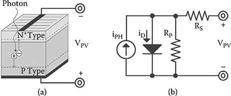
FIGURE 1.4 (a) Photovoltaic cell and (b) its corresponding electrical model.
The problem with solar energy is that output power falls drastically when direct sunlight is unavailable, down to 10–20 μW/ cm2. These power levels are so low that the act of harnessing, which is the work performed by circuits to transfer energy into a battery, may dissipate most, if not all of the power available, negating the harvesting objective of the system. Notwithstanding, a few researchers find solace in how often microsystems idle because producing any power whatsoever for extended periods still translates to appreciable energy in the long run.
Industry and research today concentrate most of their efforts on either larger scale systems, where larger surface areas compensate for the lower power densities that artificial lighting generates, or smaller photovoltaic cells that receive direct sunlight, where even 2 × 2 mm2 can generate substantial power for a microsystem. Relying on solar energy, however, limits wide-scale adoption because applications may not always place harvesting nodes in places that receive direct sunlight, so overcast days and evenings interrupt the harvesting process. Many applications, in fact, are not only indoors, like wireless microsensors in factories, hospitals, and homes, but also mobile, where the host may or may not receive sunlight, as with automobiles, bicycles, airplanes, and people. All of this is to say that harnessing artificial lighting is important, but also challenging under microscale constraints.
1.2.2 Kinetic Energy
By definition, mobile products, which represent an increasingly expansive market space, move. And from a commercial standpoint, harnessing kinetic energy from motion is attractive because vibrations are consistent and abundant—be it an engine at 1,000 to 10,000 revolutions per minute or a person at one to two strides per second. Kinetic transducers can also generate up to 200 μW/ cm2, providing the onboard harvesting microelectronics more power to operate than artificial lighting can. Although power is nowhere near what photovoltaic cells produce when exposed to direct sunlight, harnessing power from dependable 1–300 Hz vibrations over extended periods can accumulate appreciable energy.
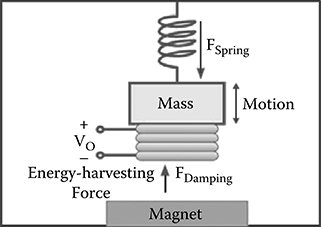
FIGURE 1.5 Transducing kinetic energy in vibrations into the electrical domain electromagnetically.
Electromagnetic transducer. One way of drawing power from motion is electromagnetically [5], by allowing vibrations to move a mass attached to a conducting coil about a stationary magnet, as Figure 1.5 illustrates. The electromagnetic field that the magnet generates works against the kinetic force in the moving mass to dampen and decelerate it, thereby transferring the energy in the mass into the coil in the form of a voltage. The role of the spring is to avoid losing remnant energy by temporarily storing and releasing whatever kinetic energy remains so that the mass may once again move back toward the magnet. Unfortunately, harnessing energy this way is difficult in small spaces because power and voltages are substantially low at approximately 1 μW/ cm3 and tens of millivolts. Additionally, conforming and integrating a magnet and a coil into a microsystem also present considerable challenges.
Electrostatic transducer. Perhaps a more effective means of harnessing ambient kinetic energy is by pumping charge electrostatically into a storage device because the power generated is on the order of 50–100 μW/ cm2 and variable capacitors are more easily integrated with MEMS technologies. The idea is for vibrations to vary the vertical or lateral separation distance between two parallel plates of a variable capacitor CVAR, like the ones that Figure 1.6(a) and 1.6(b) illustrate, so that, when a battery or another capacitor fixes the voltage across CVAR to precharge voltage VPC, a reduction in capacitance pumps charges qC out of CVAR:
and generates output dqC/ dt current [6]. Alternatively, a reduction in capacitance raises CVAR’s vC when CVAR is disconnected (i.e., with a fixed qC) to augment CVAR’s energy EC:
This latter scenario produces a net energy gain because, while CVAR decreases linearly in EC, rises quadratically. Allowing vC to increase to, say, 100–300 V, however, which is not atypical, exceeds the breakdown limits of most standard CMOS and BiCMOS process technologies. As a result, at least for the time being, constraining vC to voltages that near the breakdown limits of the process seems more practical than fixing qC.
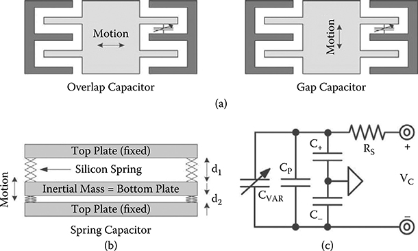
FIGURE 1.6 (a) Top and (b) vertical views of variable MEMS parallel-plate capacitors or varactors and (c) their corresponding electrical model.

FIGURE 1.7 (a) Shimmed piezoelectric cantilever and (b) its corresponding electrical model.
The electrical equivalent of these moving parallel plates is the variable-capacitor model that Figure 1.6(c) shows. Unfortunately, the physical device also includes parasitic static capacitors CP, C+, and C–. Contact material also introduces a series of parasitic resistance RS that dissipates ohmic power. Of these, CP, C+, and C– are often more problematic because they drain some of the energy that CVAR harnesses from motion.
Piezoelectric transducer. Although piezoelectric transducers are perhaps more difficult to integrate, they can generate higher power, up to maybe 200 μW/ cm2. Here, when fastened to a stationary base, as Figure 1.7(a) illustrates, a shimmed piezoelectric cantilever generates electrical energy in the form of alternating charge when mechanical energy in motion induces the material to bend and oscillate about its fixed point [7]. The advantages of this approach are that piezoelectric research is relatively mature in its evolution and transducers generate higher power than their electrostatic and electromagnetic counterparts. The disadvantage, of course, is integrating the device into a small space, which is why attaching it to the outer surface of a chip is probably one of the best ways of realizing a small SoP platform.
Operationally, motion rearranges and polarizes the molecular structure of a piezoelectric material to generate charge. The resulting electrical current, which iPZ in Figure 1.7(b) models, charges and discharges the capacitor CPZ that appears across the terminals of the transducer. The magnitude and direction of iPZ change with the acceleration and orientation of the moving mass. Unfortunately, contacts and leakage paths introduce series and parallel resistances RS and RP, but not to the extent that they negate the harvesting benefits of the structure. Ultimately, the energy that CPZ receives is the power the transducer draws from motion, which returns to the mechanical domain when uncollected.
1.2.3 Thermal Energy
Temperature represents another source of energy. Thermocouples that rely on the Seebeck effect, for example, derive thermal energy from a temperature difference. Here, as in Figure 1.8(a), heat flux carries dominant charge carriers: electrons in n-type and holes in p-type materials, from high-to low-temperature regions, much like diffusion carries particles from high-to low-concentration regions. Here, however, departing electrons in the n-material leave behind ionized molecules in the hot side that attract the electrons that the p-region generates when holes drift toward the cold end. As these electrons flow from p-to n-type regions to deionize molecules, they harness thermal energy and jump to higher energy states. This way, electrons accumulating at the cold end of the n-type rod establish a negative potential with respect to the holes that accrue at the cold side of the p-type counterpart, generating thermally induced voltages across each pile. Since each n–p pile combination generates a small voltage vTH, engineers often cascade several of these in series to produce a combined voltage vTEG, which is higher. The silicon rods and interconnecting metals, of course, introduce parasitic series resistances that RS in Figure 1.8(b) models.

FIGURE 1.8 (a) Thermocouple transducer built out of thermal piles and (b) the corresponding electrical model.
Unfortunately, high temperature alone is not sufficient to generate power. Said differently, a thermocouple generates a voltage only when a temperature differential exists. Designers, as a result, usually attach one of the terminals to a heat-absorbing material. This requirement, however, impedes integration in several ways. In the first place, a heat sink occupies considerable space. In the second, finding a cool source against which to attach the transducer is not always possible. And, thirdly, output power is proportional to the temperature difference across the device and, because microsystems are tiny, temperature differentials are correspondingly low, below maybe 10°C. The voltage and power levels they produce are consequently low at about 15 μW/ cm3 [5], which nears the levels produced by photovoltaic cells when illuminated with artificial lighting and electromagnetic transducers in response to vibrations. Note that power is also proportional to the Seebeck coefficient of the thermoelectric materials used.
1.2.4 Magnetic Energy
There is also energy in a magnetic field, such as around an AC power line. Drawing power from such a source inductively, however, is challenging in three respects. To start, as in the case of harnessing kinetic energy electromagnetically, the power levels and voltages generated are substantially low at microwatts and millivolts. Unfortunately, the act of transferring energy already dissipates microwatts and, therefore, drains most of the little power that is available. Plus, conditioning power in the form of millivolts is, from an integrated circuit’s perspective, problematic. As a result, some researchers opt to accumulate and convert magnetic energy into the mechanical domain first, so that a kinetic transducer can then generate power in a more benign form. Each conversion, however, suffers from power losses that further reduce what little energy was available in the first place.
The second issue with an electromagnetic source is that power falls drastically with distance: quadratically in the far field and even faster in the near field. Therefore, to produce practical power levels, the transducer should remain close to a rich source. Inductively coupling energy across a near-field separation of, say, 8 mm to charge the battery of a portable device like a cellular phone wirelessly is possible this way. However, increasing the separation beyond this point, which many remote wireless-sensor applications demand, lowers system efficiency to such an extent that extracting power is no longer practicable. The third challenge with harvesting magnetic energy is, of course, integration, because tiny inductors harness a small fraction of the magnetic energy available.
1.2.5 Conclusions
As mentioned earlier, there is no ideal source because, while harvesters, atomic batteries, and fuel cells store appreciable energy, they supply little power. Conversely, inductors and capacitors source high power, but stow little energy. And Li ions and super capacitors are moderate in both respects, sacrificing energy for power and power for energy. Additionally, while filter passives supply power almost instantaneously, Li ions and supercapacitors require time to respond—and fuel cells even more time—whereas atomic batteries and harvesters remain virtually unresponsive to load changes. As a result, systems today normally supply what is close to instantaneous power, which refers to the rising and falling edges of the load shown in Figure 1.1, with capacitors and semisustained bursts with a Li ion.
Relegating the tasks of storing energy and supplying power bursts to a Li ion or supercapacitor, however, represents a compromise in energy that is difficult to accept under microscale constraints where both energy-and power-density requirements are severe. Replacing the Li ion with a fuel cell similarly trades power for energy, loading capacitors and inductors with more power and, as a result, increasing output voltage variations in response either to load dumps or space requirements. Further decoupling energy from power is therefore important in microsystems, which is the motivation for classifying technologies into energy sources, energy/ power caches, and power supplies.
Harvesters, atomic batteries, and fuel cells fall under the category of energy sources. Of these, atomic batteries are less popular because they are unsafe, and costly and tiny fuel cells because they produce chemical by-products. Li ions and supercapacitors basically cache energy and power for moderate loads, but while Li ions are perhaps more mature and popular, ultracapacitors survive more charge–discharge cycles, which is why the latter are garnering interest, albeit with higher leakage. Lastly, capacitors and inductors both supply power, but only capacitors supply instantaneous current, so systems use capacitors to store charge and supply quick load dumps and inductors to supply the collective steady-state needs of the load and momentary demands of capacitors.
Of the ambient sources discussed here, solar energy generates the most power, followed by kinetic energy when harnessed by piezoelectric or electrostatic transducers. Thermal and magnetic energy are less appealing under microscale integration because their power and voltage levels are low. Similarly, artificial lighting also generates low power levels, as does drawing kinetic energy with an electromagnetic device. As a result, some engineers favor solar photovoltaic and vibration-sensitive piezoelectric and electrostatic transducers over their competing counterparts.
1.3 Conditioning Microelectronics
The role of the power-supply circuit in a system is to transfer energy from a source and condition power to supply the needs of its load. Because energy is finite and especially scarce in a microsystem, the overriding measure of success, outside conditioning, is how much of the available power PIN reaches the output as PO. In other words, power lost PLOSS across the system determines one of the most important parameters of a power supply: its efficiency η or
For example, if the load demands 100 μW and the power supply dissipates 50 μW to generate those 100 μW, the source supplies 150 μW and the system is 66.7% efficient. Similarly, in the case of harvesters, if a source supplies 100 μW, but the system dissipates 50 μW, the output only receives 50 μW at 50%.
Efficiency typically changes with output power PO because losses do not vary at the same rate. At moderate to high power levels, for example, quiescent losses usually become a smaller fraction of a rising load, so efficiency is relatively high [8]— for example, when losing 75 μW to drive a 1 mW load yields 93%. Microsystems, unfortunately, normally demand lower power levels; this means that power losses represent a larger percentage of the load—for example, when losing 50 μW to drive 50 μW is the result of 50% efficiency. What is worse, microsystems normally idle and dissipate even less power—maybe 1–10 μW. Under these idling conditions, operational life is especially sensitive to power losses because the lifetime difference of a 1 μW and a 9 μW loss under a 10 μW load is close to 70%, or 1.7 times, and under a 100 μW load is 10%, or 1.1 times; dissipating less than 1 μW is extremely difficult, if not impossible, when powering alert functions and other vital blocks in the system. All of this is to say that light-load efficiency is probably one of the most difficult challenges to tackle in a microsystem, especially when the act of conditioning, in and of itself, requires work.
1.3.1 Linear Switch
Perhaps the most accurate means of conditioning power is linearly because the circuit is always alert, ready to respond to any and all variations in load and source. In other words, in addition to not generating switching noise, a linear conditioner reacts to oppose the effects of disturbances injected and coupled into its output. Admittedly, the circuit suppresses noise only up to its bandwidth [9], beyond which the system is unable to respond. Nevertheless, a linear circuit is relatively simple, so it reaps the high-bandwidth benefits that smaller devices and fewer transistors offer.
Architecturally, as Figure 1.9 shows, a controller modulates the conductance of a series switch linearly to conduct whatever current the system demands. In the case shown, p-channel metal–oxide semiconductor (MOS) field-effect transistor (FET) MSW is only a sample, though a popular embodiment of the switch. Low-dropout (LDO) linear regulators, for example, use this topology and sample output voltage vO to ensure that vO remains near a user-defined target. To illustrate another application, sensing input current iIN and regulating MSW’s conductance or equivalent series resistance RSW to draw as much iIN as the source allows satisfy the objectives of a harvester.
Irrespective of its conditioning aim, what is ultimately important to conclude is that the circuit does not generate switching noise; current iIN only flows to the output (i.e., in one direction), so input vIN must exceed output vO, and the circuit dissipates conduction power across MSW as PSW:
and quiescent power through the controller as PC for a total power loss PLOSS of
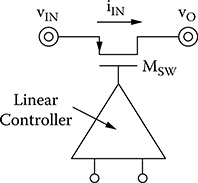
FIGURE 1.9 Basic architecture of a linear conditioner.
where vIN – vO is the voltage across MSW and IQ that the current vIN supplies to the controller. Although all three points are important, the last one deserves attention because microsystems cannot afford to lose power indiscriminately. Efficiency here, in fact, cannot ever reach output-to-input voltage ratio vO / vIN because the voltage across MSW is vIN – vO and IQ is a finite and load-independent physical requirement for the circuit to operate properly:
Consider, for example, that when a 3.6 V Li ion supplies a 1.8 V load, ηL is no better than 50%, and that is only when IQ is negligibly smaller than iIN, which is largely not the case in microsystems, particularly when they idle.
1.3.2 Switched Capacitors
Introducing one or more intermediate steps into the energy-transfer process further decouples the needs of the input from those of the output, adding flexibility to the conditioning function. A transitional stage, therefore, receives, stores, and releases energy when prompted, as a capacitor would when configured accordingly. Charge pumps, as many circuit design engineers refer to them, switch the connectivity of “flying” capacitors in alternating phases across a switching period TSW to first receive energy from a source, be it the actual input or a previous stage, and then release it to a load, which could be just another stage. Charging several flying capacitors in parallel, for instance, from input vIN, as CF1 through CFN illustrate in Figure 1.10, and discharging them in series to a load effectively “steps up” or “boosts” the input vIN to a higher voltage vO, which is an otherwise impossible feat for a linear conditioner to achieve. Similarly, just to show how flexible the architecture can be, charging capacitors from vIN in series and connecting them in parallel to vO in the alternate phase “steps down” or “bucks” vIN to a lower voltage.

FIGURE 1.10 Switching phases of a boosting two-step switched-capacitor charge pump.
This flexibility, however, results at the expense of noise because decoupling vIN from vO implies that vIN and vO are, at times, disconnected, so iIN momentarily raises vIN and the load similarly discharges whatever output capacitance CO is present at vO. Allowing vIN and vO to rise and fall this way before periodically loading and recharging them with the flying capacitors creates a systematic noise ripple in the input and output. To this, the switches whose task is to reconfigure the connectivity of the network, inject additional noise because the signals that drive them at switching frequency fSW rise and fall quickly across maybe 10 ns or less—coupling displacement noise energy into sensitive nodes through parasitic gate-source and -drain capacitors CGS and CDG that complementary MOS (CMOS) switches embody.
Because the voltages across conducting switches are dynamic and decrease with time, switched-capacitor circuits do not dissipate the quasistatic and limiting vIN -vO voltage-drop conduction power that linear conditioners do across MSW. Still, the switches lose momentary switching losses when conducting current with decreasing, but nonetheless, finite voltages across them. The initial voltage across the switch that connects vIN to the flying capacitors in phase 1 of Figure 1.10, for example, is the voltage the load drooped in phase 2, which is often not a trivial amount. Similarly, the fully charged flying capacitors and the drooped CO also present a voltage difference to their connecting switch at the beginning of phase 2. To help quantify these losses, consider that while vIN in Figure 1.11(a) loses energy EIN to charge equivalent flying capacitor CF from vC(INI) to vIN:
CF‘s energy EC rises from EC(INI) to EC(FIN) for a positive gain of ΔEC:
which is nonetheless a fraction of EIN, so the switch loses the difference [10] as ESW:
Similarly, because connecting capacitors in parallel like in Figure 1.11(b) amounts to charging them in series from a source whose voltage is the initial voltage across the switch vC(INI) -vO(INI) or ΔvSW, the switch consumes
of the energy that was initially stored in CEQ as 0.5 , where CEQ is the series combination of CF and CO. In other words, charge pumps generally and necessarily lose switching energy 0.5 in the interconnecting switches.
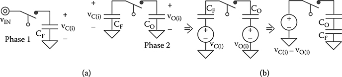
FIGURE 1.11 Charging a capacitor with a switch from (a) an input source and (b) another capacitor.
Although this fundamental loss in the switch is by no means negligible, it decreases with reductions in steady-state iIN(AVG) because all the capacitors droop less (so ΔvSW is smaller) with lower currents, which is good for microsystems because they supply and demand little power. In practice, however, vIN still supplies the energy switching noise and leakage currents drawn from the capacitors, the quiescent power that energizes the controller, and the power parasitic gate and base capacitors require charging and discharging every time they switch. So to summarize, a charge pump generates switching noise, can buck or boost its input, and dissipates 0.5 across interconnecting switches, which rises quadratically with iIN(AVG). Relative to its linear counterpart, the output is noisy and less accurate, but also flexible. The circuit also impresses voltages across the switches that decrease not only with load but also with time. Additionally, charge pumps dissipate power to charge and discharge parasitic capacitors that would normally not switch periodically in a linear conditioner.
1.3.3 Switched Inductor
Just as charge pumps employ capacitors to transfer energy, magnetic-based switching converters use inductors to cache and release input energy temporarily to one or several loads [11]. They achieve this by energizing and draining inductors in alternating cycles. In more specific terms, an input source vIN energizes a transfer inductor LX by inducing LX to draw current from vIN—that is, by connecting the other terminal of LX to a lower voltage like ground in phase 1 of Figure 1.12(a). During this time, LX’s current iL rises linearly, as the graph in Figure 1.12(b) shows, because LX’s voltage vL or LXdiL/ dt is positive and, for the most part, constant at, in this case, vIN – 0, or more generally, at energizing voltage vE. Reversing the polarity of vL to, say, –vO, as shown in phase 2 of Figure 1.12(a), causes LX to release the energy it received during phase 1. Because the circuit either regulates the voltage across a load or charges a battery with a well-defined, low-ripple, slow-changing voltage, vO is, for all practical purposes, a constant and, in this case, also LX’s de-energizing voltage vDE. As a result, iL generally rises at vE/ LX when vIN energizes LX across phase 1 and falls at vDE/ LX when LX delivers energy to vO in phase 2 [12].
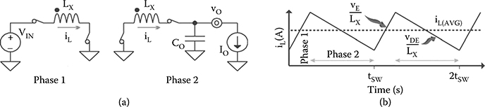
FIGURE 1.12 (a) Switching phases of a switched-inductor converter and (b) the time-domain response of its inductor current.
A switched-inductor conditioner embodies a few idiosyncrasies worth mentioning. First, LX conducts a steady-state current iL(AVG) about which the ripple in Figure 1.12(b) rides. Conducting current continuously like this places the circuit in what experts call continuous-conduction mode (CCM). Inducing LX to stop conducting current momentarily, which is equivalent to iL reaching zero and remaining there for a finite fraction of the period, amounts to operating in discontinuous-conduction mode (DCM). What sets iL(AVG) is either the power needs of a load or the sourcing capabilities of its source.
Another trait or, rather, feature is that a switched-inductor circuit can buck or boost vIN because LX can release energy to any output voltage as long as energizing and de-energizing voltages vE and vDE remain positive and negative, respectively. In fact, permanently attaching LX’s input terminal to vIN is a derivative embodiment of the general form shown in Figure 1.12(a) that, to release LX’s energy, requires vO to exceed vIN. Likewise, connecting LX’s output terminal to vO directly demands that vIN stay above vO for LX to energize. These two special cases implement the well-known boost [13] and buck [14] configurations reported in the literature. One last peculiarity to note is that inductors, unlike capacitors, receive or deliver energy, but do not store it statically over time; this is not a problem in conditioners because the overriding aim is to draw and deliver power—not store it, as rechargeable batteries and large capacitors would.
Within the context of operational life and efficiency, the only elements in a power stage that incur first-order conduction losses are the switches because a capacitor does not conduct steady-state current and the steady-state voltage across an inductor is zero. Interestingly, while capacitors hold the initial voltage across a switch by sourcing whatever instantaneous currents are necessary, an inductor maintains its current steadily by instantly swinging its voltage until it finds a suitable source or sink for its current. In other words, after a connecting switch opens, iL raises or lowers LX’s open terminal voltage instantaneously until a source or sink clamps it. As a result, the small series resistance RSW in the interconnecting switches and power path drop a voltage vSW or iLRSW that consumes power PSW or iL(RMS)2RSW. Since RSW is small, vSW and PSW are both low. This quasi-lossless property is the driving force behind the commercialization and general adoption of switched-inductor conditioners.
In practice, these conduction losses are small, but nevertheless finite, so they reduce efficiency, as do second-order losses similar to those found in linear and charge-pump circuits. The controller, for example, requires sufficient quiescent current to manage the system and deliver a command signal in time before the onset of the next switching cycle. The circuit also dissipates switching power to charge and discharge the parasitic capacitors that the switches present to the controller. When lightly loaded, in fact, second-order quiescent and gate-drive losses become as important as and, in some cases, more important than first-order switch losses because the voltage dropped and power lost across the switches fade with decreasing load levels [15].
Note, however, that good and reasonably sized power inductors are bulky and difficult to integrate [16]. The unfortunate truth is that on-chip inductances typically fall below 100 nH and introduce considerable parasitic equivalent-series resistances (ESRs) that further dissipate conduction power and degrade efficiency. Discrete inductors, on the other hand, are considerably better and, to a certain extent, also relatively small—for example, a 2 × 2 × 1 mm3 1 μH inductor that saturates at 1.8 A and introduces 0.2 × of series resistance. Accordingly, switched-inductor conditioners in microsystems should employ and co-package no more than one power inductor, which is why single-inductor multiple-output (SIMO) strategies are garnering interest in research circles [11]. Using smaller inductances is certainly possible, though at the expense of higher conduction losses because inductor ripple current ΔiL increases or gate-drive losses because switching frequency fSW rises to bound ΔiL.
Because these magnetic-based circuits switch, they inject switching noise, like charge pumps do. If LX connects directly to vIN or vO, however, as in boost or buck converters, LX’s average current iL(AVG) matches the source or load to keep the capacitance at vIN or vO from charging or discharging considerably. Even so, vIN and vO do not source or sink ripple currents, so ΔiL charges and discharges CIN or CO to create a corresponding ripple in vIN or vO. Unfortunately, decoupling the input or output from LX with a switch, as in buck or boost converters, allows the source or load to charge or discharge CIN or CO when the switch opens, increasing the ripple in vIN or vO. In all, these magnetic conditioners generate switching noise, can buck or boost their inputs, dissipate iL(RMS)2RSW across their interconnecting switches that rises quadratically with iIN(AVG), and, when applied to microsystems, should employ no more than one co-packaged inductor.
1.3.4 Conclusions
In comparing performance, the functionality of the conditioners precedes all other parameters, and in the case of microsystems, losses arguably follow because they limit how long a system operates. So, on the first count, switching circuits can boost their inputs while linear circuits cannot—except that a boosting function is not always necessary. Consider, for example, that while boosting a 0.4 V photovoltaic cell to charge a 2.7–4.2 V Li ion requires a switching circuit, bucking a 2.7–4.2 V Li ion to supply a 1.8 V load does not.
From the perspective of power, as summarized in Table 1.1, the switch in a linear circuit drops vIN – vO continuously, whereas the terminal voltages across the switches in a charge pump and a switched inductor decrease with load and across time. In other words, switched circuits can dissipate less power than their linear counterparts. Switched capacitors, however, typically require more switches to implement than switched inductors, so capacitor networks dissipate more gate-drive losses PGD.
TABLE 1.1 Comparing Conditioning Circuits
| vo | Firsr-Order Loss PsW | Second-Order Losses | Switching Noise | |
Linear |
<vIN |
iIN(vIN – vO) |
PQ |
None |
Switched C |
≤ ≥vIN |
PQ + PGD |
∝ iIN(AVG), CPAR, 1/fSW |
|
ΔvSW ∝ iIN(AVG), t |
||||
Switched L |
≤ ≥vIN |
PQ + PGD |
∝ ΔiL ∝ 1/LX, 1/fSW |
|
iL(RMS) ∝ iIN(AVG) |
And maybe iIN(AVG), CPAR |
Switch losses in all three cases, however, diminish with load, so when microsystems idle, efficiency is more sensitive to second-order losses, which is where linear circuits might gain an edge because they do not dissipate gate-drive power PGD. The problem is that miniature devices demand little to no power when idling and moderate to substantial power when transmitting data wirelessly, so a linear circuit is more appealing when idling and less appealing otherwise, and vice versa for a switched inductor. In the end, functionality may become the deciding factor, which is why operating in DCM and reducing switching frequency fSW in magnetic-based converters is so important when the load is light, as is lowering quiescent power PQ in all three schemes. Notice, by the way, that parasitic series resistances in the inductor, capacitors, and board also dissipate ohmic losses.
Noise in the output may not be a problem for charging a Li ion but is certainly an issue when supplying a functional load like a data converter or sensor-interface circuit whose sensitivity to noise in the supply is often severe. Noise at the input is similarly problematic when drawing power from a PV cell because raising the voltage increases the current lost to the parasitic diode present and letting it drop lowers how much current the cell generates. Linear switches outshine their switching counterparts in this regard because they never disconnect from vIN or vO. Ripple current ΔiL in switched-inductor circuits, of course, adds noise. Charge pumps are probably the worst because flying capacitors momentarily and necessarily disconnect from vIN and vO. Switched-inductor circuits that decouple the outputs from the inductor also suffer from similar effects, in addition to the ΔiL-induced noise already mentioned. Ultimately, reducing noise amounts to raising fSW (to shorten how long vIN and vO float) and circuit bandwidth (to keep up with fSW), and, in the case of inductor circuits LX (and fSW), to reducing ΔiL. Increasing fSW, however, by and large degrades efficiency, and raising LX demands more space, which is the conundrum engineers eventually face when designing these types of circuits: when and how to trade accuracy, efficiency, and integration.
1.4 Energy-Harvesting Chargers and Power Supplies
The conditioners described in the last section form the foundation from which modern chargers and power supplies draw inspiration. Since no converter is ideal, engineers first prioritize specifications and then choose one or a combination of approaches according to the most important parameters in the system. In a cellular phone, for example, battery life is as sensitive to conversion efficiency as a large fraction of the load is to noise in the supply. In such a case, a switched-inductor converter bucks a Li ion voltage efficiently to a level that minimizes the power lost across a cascaded linear voltage regulator, whose purpose is to filter the noise that the switcher generates in the first place and supply the power that the sensitive load demands. In a harvester, saving energy is the chief objective, so an efficient switched-inductor charger might fit the bill, if power levels are sufficiently moderate for conduction losses to remain significant. Note that supplying a functional load requires a voltage source and feeding a battery a current source or charger, and while circuits may generate these without feedback, shunt-or series-sensed control loops often modulate the conductance or duty-cycle operation of the conducting switches to regulate them [17].
Space in miniature systems is so constricting that using a single sourcing technology represents a sacrifice in energy, power, or both. In these applications, complementing the energy features of ambient energy with the power-generating capabilities of Li ions and ultracapacitors offers appealing qualities that no one source can. Justifying the need for both energy and power, however, is imperative [18] because a hybrid supply is necessarily more complex than a single-source system. From this viewpoint, most microsystems, like wireless microsensors, idle and communicate information wirelessly, so their power range is vast and as critical as energy because the latter sets operational life. Hybrid supplies in tiny devices are therefore justifiable.
1.4.1 Battery-Assisted Photovoltaic Charger–Supply Example
The switched inductor in Figure 1.13 draws power from both a 0.25–0.4 V PV cell vPV and a 1.8 V power source vPS or battery to supply a 1 V load [19]. Relying on only one small off-chip power inductor LX is important because off-chip inductors are bulky and their on-chip counterparts are poor, but altogether excluding the inductor drastically reduces power-conversion efficiency. Input and output capacitors CIN and CO are also critical because they help keep LX, the PV cell, and load currents iL, iPV, and iO from slewing vPV away from its maximum-power point and output vO away from its target VREF.
When lightly sourced, LX draws and delivers energy to vO—first from vPV and then from vPS. For this, switches SPV and SE energize LX from vPV, and SPV and SO subsequently drain LX into vO. After that, SPS and SO similarly energize LX, and SDE and SO de-energize LX into vO. Otherwise, when heavily sourced, LX supplies PO to the load from vPV and charges vPS with what remains of PPV. As before, SPV and SE energize LX, and SPV and SO drain LX into vO, but unlike before, SO opens after vO receives sufficient energy to satisfy PO, and iL therefore charges switching node vSW.O until diode DPS forward-biases and charges vPS with iL.
The PV cell generates the most power when vPV nears its optimal value of VPV(OPT), which means that this system should adjust vPV to VPV(OPT). Since the switching network induces a ripple voltage in vPV that shifts the PV cell from its maximum-power point, vPV’s ripple ΔvPV should be small. The circuit should also be able to modify and track vPV to new targets to accommodate changes in light intensity and conditions.
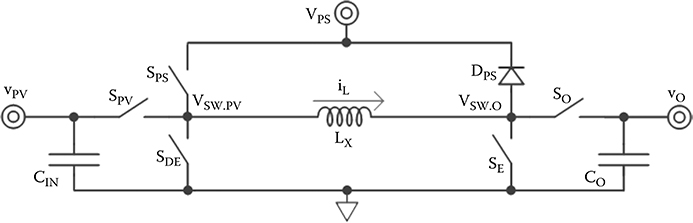
FIGURE 1.13 Battery-assisted photovoltaic buck–buck charger supply.
Harvesting performance hinges on reducing power losses. Considering this, tiny PV cells generate microwatts, ensuring that LX conducts continuously without reversing the direction of current amounts to keeping its rippling current ΔiL within a small window, which happens when LX switches quickly. Charging and discharging the gates of power switches more often, however, requires more power, which is why LX should not conduct continuously and should switch slowly.

FIGURE 1.14 Photovoltaic-voltage and inductor-current time-domain waveforms.
To ensure that LX derives sufficient PV power PPV in one energizing (tE) and de-energizing (tDE) sequence, iL rises and peaks to iL(PK) (about 6 mA in Figure 1.14). Transferring a larger energy packet EPV in 1.6 μs draws sufficient PPV from vPV to keep vPV from rising excessively over VPV(OPT) across the remaining 11.4 μs of the 13 μs period TSW. Had EPV been smaller and TSW shorter, ΔvPV would have been less than 20 mV; however, the power lost in switching more often negates the benefits of a smaller ripple.
Selecting the channel width–length ratios of the switches that balance conduction and gate-drive losses in the system and choosing the iL(PK)–TSW combination that reduces the percentage of PV power PPV lost to PLOSS enable the PV cell to supply the load fully or partially and, when possible, recharge the battery. When lightly loaded, the system regulates vO and steers excess PPV to the battery to charge vPS in staircase fashion, as Figure 1.15 shows. When lightly sourced, the system draws both PV and battery power to supply and regulate the load.

FIGURE 1.15 Battery-charge profile when heavily sourced.
1.4.2 Piezoelectric Charger Example
Drawing power from an intermittent source to supply the needs of an unpredictable and uncorrelated load is challenging. As a result, harvesting and regulation are often separate and distinct functions in a microsystem. While a regulator, for example, supplies a load from a battery, a harvester can charge the battery. So, in the more specific case of tiny piezoelectric conditioners, chargers convert and condition rippling sources to replenish capacitors, rechargeable batteries, or a combination of both capacitors and batteries.
Typical battery-supplied implementations use a bridge-based rectifier to convert an alternating signal into a steady-state voltage that subsequently feeds another converter whose aim is to condition and steer power into a battery. Unfortunately, each conditioning function dissipates power, and, collectively, they diminish the gains of a microscale harvester. To minimize this loss, the piezoelectric charger in Figure 1.16 combines rectification and conditioning into one stage [20]. The underlying aim is to derive power from positive piezoelectric voltages with harvesting inductor LH and reverse LH’s current flow to draw energy from negative voltages.
First, through vPZT’s positive half cycle in Figure 1.17, switches SI and SN remain open to decouple the power stage from the transducer until vPZT reaches its positive peak. SI and SN then engage (at 15.73 ms) to discharge CPZT into LH, until iL peaks. Since LC resonance drives this energy transfer, the system estimates LH’s energizing time by waiting for one-quarter of LH–CPZT’s resonance period at 0.5 π√(LHCPZT). Note that sensing iL’s peak directly is more accurate, but also considerably more lossy. After this, SN opens and iL charges the parasitic capacitance at switching node vSW+ quickly until noninverting diode-switch DN forward biases and depletes LH into VBAT. During the negative half cycle, SI and SN again open to disconnect the circuit from the transducer until vPZT reaches its negative peak. Afterward, SI and SN discharge CPZT into LH (at 20.69 ms) for one-quarter of LH–CPZT’s resonance period. SI then opens and DI conducts iL into VBAT. This way, the system deposits energy into VBAT every half cycle in staircase fashion, as Figure 1.18 illustrates under vibrations of various strengths.

FIGURE 1.16 Single-inductor energy-harvesting piezoelectric charger.

FIGURE 1.17 Time-domain waveforms.

FIGURE 1.18 Battery-charge profile.
1.4.3 Electrostatic Charger Example
Harnessing energy from a variable capacitor CVAR is possible because the work that vibrations exert to separate the conducting plates decreases the device’s capacitance. As a result, because charge qC is the product of CVAR and its voltage vC or CVARvC, reducing CVAR raises vC, and the quadratic gain that vC2 represents in energy 0.5 CVARvC2 overwhelms CVAR’s linear drop. Unfortunately, vC often rises to 100–300 V, well beyond the breakdown limits of low-cost CMOS process technologies.

FIGURE 1.19 Electrostatic harvesting sequence.
Alternatively, clamping CVAR to a large reservoir capacitor CRES precharged to VCLAMP constrains vC and causes qC to fall in response to reductions in CVAR, which means that CVAR drives charge into CRES. The cycle-by-cycle progression shown in Figure 1.19 does just this: first, precharges CVAR to VCLAMP and then connects CVAR to CRES so that reductions in CVAR pump charge into CRES. Afterward, the system disconnects CVAR, recovers remnant energy in CVAR, and collects harvested charge into CRES. After vibrations finish resetting CVAR to CMAX, the system starts another harvesting cycle by again precharging CVAR to VCLAMP [21].
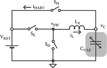
FIGURE 1.20 Battery-clamped electrostatic harvesting charger.
Unfortunately, breakdown voltages in modern CMOS process technologies are low at 1.8–5 V. This means that the energy CVAR holds at CMIN with VCLAMP can be so low that conduction and gate-drive losses in the recovery process can dissipate most, if not all of CVAR’s energy. In these cases, skipping the recovery phase and clamping CVAR directly to VBAT (instead of CRES) during the harvesting phase are prudent design choices because they reduce the sequence to precharge, harvest (to VBAT), and reset and eliminate lossy energy-transfer transactions between CRES and VBAT. The switching network of Figure 1.20 does just this: Precharge CVAR at CMAX from VBAT with switches SE and SD and inductor LX, connect CVAR to VBAT and harvest CVAR’s charge directly to VBAT through SH when CVAR falls to CMIN, and disconnect all switches to allow vibrations to reset CVAR to CMAX.
In this simplified progression, there are only two energy transfers: when pre-charging CVAR and harvesting into VBAT. For the first, while using a switch to connect and precharge CVAR at CMAX to VBAT is simple, it is also the lossiest option because the switch consumes 0.5CMAXVBAT2. This is the reason that SE starts the precharge phase by energizing inductor LX from VBAT and SD subsequently drains LX into CVAR [22]. Notice that CVAR also charges when LX energizes, so LX caches only part of the energy that CVAR ultimately receives when LX finishes de-energizing into CVAR.
Since CVAR precharges to VBAT (at 0 and every 33 ms after that in Figure 1.21), connecting CVAR to VBAT after precharge with SH draws no current and, therefore, no power from either CVAR or VBAT. Afterward, through the first 16.5 ms of every cycle in Figure 1.21, CVAR falls to CMIN to drive harvesting current iHARV into VBAT via SH. Because iHARV is low, SH dissipates little power across this phase. When CVAR reaches CMIN (at 16.5 and every 33 ms after that in Figure 1.21), all switches disconnect and, through the ensuing 16.5 ms, vibrations separate CVAR’s plates until CVAR rises to CMAX, at which point another cycle begins.

FIGURE 1.21 Battery-constrained electrostatic harvesting charger.
As with every harvesting system, the ultimate goal is to generate sufficient power to output a net energy gain. The challenge is that miniature transducers generate little power and conditioning circuits can easily dissipate much of that power. In the electrostatic case presented, VBAT invests as EINV to charge CVAR to VBAT at CMAX and harvests energy from CVAR as CVAR falls to CMIN. As a result, VBAT loses energy when the cycle begins (at 0 and every 33 ms after that in Figure 1.21) and harvests energy every half cycle after that to produce the staircase response in Figure 1.21. In other words, CVAR generates more energy EOUT than the system invests in EINV and dissipates in ELOSS:
where EOUT is the charge energy that VBAT receives as ΔQCVBAT or (ΔCVARVBAT)VBAT when CVAR falls to CMIN and ΔCVAR is the difference between CMAX and CMIN. An important observation to note here is that output power from EHARV is ultimately higher with larger CMAX–CMIN spreads and lower power-conditioning losses.
1.4.4 Conclusions
Hybrid supplies in microsystems generally suffer from full-scale integration and poor low-power efficiency. Tiny spaces, to start, constrain energy to such an extent that efficiency concerns overwhelm all other performance metrics, which means switched-inductor conditioners become almost indispensable. Power inductors, unfortunately, are bulky and difficult to integrate; this means that miniaturized chargers and supplies cannot afford to use more than one. And even if they are more efficient than linear and switched-capacitor implementations under moderate to heavy loads, magnetic-based supplies still dissipate conduction, gate-drive, and quiescent power. In fact, a fundamental challenge that designers face in ultra low-power chargers and supplies is keeping gate-drive and quiescent losses low—that is, managing complex systems with little to no power.
Harvesters bear the additional burden of synchronizing circuits to often unpredictable and uncorrelated ambient events and conditions. Not only that, starting and operating a system with no initial energy is especially problematic. Many implementations, therefore, rely on a battery storing sufficient initial charge to bias and start the system, much like cars depend on charged batteries to ignite their engines. In other words, ultrasmall solutions often complement a harvesting source with another technology, like a battery with some charge, to ensure that the system starts properly.
1.5 Summary
The potential market space for miniature systems like wireless microsensors is vast. One contributing factor is that adding intelligence to expensive and difficult-to-replace infrastructures nonintrusively has the potential of updating and improving otherwise obsolete and archaic technologies of scale. Power grids can manage not only energy more efficiently with embedded instrumentation but also military base camps, space stations, industrial plants, hospitals, farms, and others. Biomedical implants and portable and wearable consumer electronics also reap the benefits of microscale integration. Tiny spaces, however, limit energy and power, and modern mixed-signal systems demand both: energy for operational life and power for functionality, like sensing, data processing, and wireless transmission.
Sadly, no single miniature source is ideal. While capacitors and inductors source high power, for example, they store little energy. Fuel cells and nuclear batteries may store more energy, but they supply considerably less power. Li ions and ultra-capacitors are moderate in almost every way; however, sacrificing energy for power, or vice versa, for the sake of adopting only one technology (for low cost) is quickly becoming less viable under microscale constraints. From this perspective, harvesting ambient energy is a good way of replenishing and complementing a power-dense device that is easily exhaustible. In fact, harvesters do not release the by-products that fuel cells do, nor do they impose the safety hazards or cost infrastructure that nuclear batteries do.
Harnessing solar energy generates the most power at several milliwatts per square centimeter; however, direct sunlight is not always available and artificial lighting outputs substantially lower power levels on the microwatt per square centimeter range. Unfortunately, deriving power from thermal and magnetic sources in small spaces not only produces millivolt signals that are difficult to condition but also generates only microwatts per cubic centimeter. Although kinetic energy in motion cannot generate the milliwatts that photovoltaic cells can when exposed to solar light, vibrations are abundant and consistent, and piezoelectric and electrostatic transducers are capable of producing moderate power levels from vibrations at around 100–300 μW/ cm3. All the same, research continues and the final verdict on the power capabilities of light, thermal, magnetic, and kinetic transducers is far from certain.
Irrespective of the source, conditioning microwatts is difficult because the mere act of transferring energy can dissipate much of the little power that is available. Linear converters, for example, may be noise free, simple, and relatively fast, but their conducting switches dissipate ohmic losses that only decrease linearly with output current. And while losses in switched capacitors decrease quadratically with load, switched inductors, whose losses also decrease at a similar rate, employ considerably fewer switches, so gate-drive losses are corresponding low. At microwatts, though, quiescent and switching losses become more significant, obscuring the boundary regions where one conditioner’s efficiency clearly outperforms that of another.
Mixed-signal microsystems often reduce losses and increase integration densities by mixing multiple sourcing technologies with magnetic-based converters that use only one inductor. Irrespective of the combination, hybrid supply circuits must carefully manage energy and power flow for maximum life and accurately condition power to supply a load and/ or replenish a battery fully. Directing how and where power flows from a tiny photovoltaic cell with only a single inductor, for example, is as important as charging a co-packaged thin-film Li ion and regulating the voltage across a load. How circuits load transducers, charge batteries, and synchronize to ambient conditions eventually sets the operational life of a system. Designers must therefore implement these and other basic functions without exhausting or stressing the tiny sources in the microsystem; in other words, engineers must design circuits that perform relatively complex tasks with little to no energy.
References
1. G. A. Rincón-Mora, and M. Chen. 2005. Self-powered chips—The work of fiction. Power Management Design Line (PMDL). April 28, 2005 (http://www.eetimes.com/design/power-management-design/4011558/Self-powered-chips—The-work-of-fiction).
2. B. Sahu, and G. A. Rincón-Mora. 2004. A high-efficiency linear RF power amplifier with a power-tracking dynamically adaptive buck-boost supply. IEEE Transactions on Microwave Theory and Techniques 52 (1): 112–120.
3. M. Chen, J. P. Vogt, and G. A. Rincón-Mora. 2007. Design methodology of a hybrid micro-scale fuel cell-thin-film lithium ion source. IEEE International Midwest Symposium on Circuits and Systems (MWSCAS), Montreal, Canada, August 5–8, 2007.
4. E. O. Torres, and G. A. Rincón-Mora. 2008. Energy-harvesting system-in-package (SiP) microsystem. ASCE Journal of Energy Engineering 134 (4): 121–129.
5. E. O. Torres, and G. A. Rincón-Mora. 2005. Long lasting, self-sustaining, and energy-harvesting system-in-package (SiP) sensor solution. International Conference on Energy, Environment, and Disasters (INCEED), Session A-2, ID 368, pp. 1–33, Charlotte, NC, July 2005.
6. E. O. Torres, and G. A. Rincón-Mora. 2009. Electrostatic energy-harvesting and battery-charging CMOS system prototype. IEEE Transactions on Circuits and Systems (TCAS) I 56 (9): 1938–1948.
7. D. Kwon, and G. A. Rincón-Mora. 2009. A rectifier-free piezoelectric energy harvester circuit. IEEE International Symposium on Circuits and Systems (ISCAS), Taipei, Taiwan, May 24–27, 2009.
8. G. A. Rincón-Mora. 2009. Power IC design—From the ground up. Blackfoot, ID: Rocky Mountain Publishing.
9. V. Gupta, G. A. Rincón-Mora, and P. Raha. 2004. Analysis and design of monolithic, high PSR, linear regulators for SoC applications. Proceedings of IEEE International System on Chip (SOC) Conference, 311–315, Santa Clara, CA.
10. G. A. Rincón-Mora. 2005. Power management ICs: A top-down design approach. Raleigh: Lulu.com.
11. D. Kwon, and G. A. Rincón-Mora. 2009. Single-inductor multiple-output (SIMO) switching DC–DC converters. IEEE Transactions on Circuits and Systems II (TCAS II) 56 (8).
12. D. Kwon, and G. A. Rincón-Mora. 2009. Operation-based signal-flow AC analysis of switching DC–DC converters in CCM and DCM. IEEE International Midwest Symposium on Circuits and Systems (MWSCAS), Cancún, Mexico, August 2–5, 2009.
13. N. Keskar, and G. A. Rincón-Mora. 2008. A fast, sigma-delta boost DC–DC converter tolerant to wide LC filter variations. IEEE Transactions on Circuits and Systems (TCAS) II 55:198–202, February 2008.
14. H. P. Forghani-zadeh, and G. A. Rincón-Mora. 2007. An accurate, continuous, and lossless self-learning CMOS current-sensing scheme for inductor-based DC–DC converters. IEEE Journal of Solid-State Circuits 42 (3): 665–679, March.
15. S. Kim, and G. A. Rincón-Mora. 2009. Achieving high efficiency under micro-watt loads with switching buck DC–DC converters. Journal of Low Power Electronics (JOLPE) 5 (2): 229–240.
16. G. A. Rincón-Mora, and L. A. Milner. 2005. How to fully integrate switching DC–DC supplies with inductor multipliers. Planet Analog, eetimes.com, December 18, 2005.
17. G. A. Rincón-Mora. 2009. Analog IC design: An intuitive approach. Raleigh: Lulu.com.
18. M. Chen, J. P. Vogt, and G. A. Rincón-Mora. 2007. Design methodology of a hybrid micro-scale fuel cell-thin-film lithium ion source. IEEE International Midwest Symposium on Circuits and Systems (MWSCAS), Montreal, Canada, August 5–8.
19. R. Damodaran, and G. A. Rincón-Mora. 2013. Battery-assisted and photovoltaic-sourced switched-inductor CMOS harvesting charger–supply. IEEE’s International Symposium on Circuits and Systems (ISCAS), Beijing, China, May 19–23.
20. D. Kwon, and G. A. Rincón-Mora. 2010. A 2 μm BiCMOS rectifier-free AC–DC piezoelectric energy harvester-charger IC. IEEE Transactions on Biomedical Circuits and Systems (TBioCAS) 4 (6): 400–409.
21. E. Torres, and G. A. Rincón-Mora. 2009. Energy budget and high-gain strategies for voltage-constrained electrostatic harvesters. IEEE International Symposium on Circuits and Systems (ISCAS), Taipei, Taiwan, May 24–27, 2009.
22. E. O. Torres, and G. A. Rincón-Mora. 2009. Electrostatic energy-harvesting and battery-charging CMOS system prototype. IEEE Transactions on Circuits and Systems (TCAS) I 56 (9): 1938–1948.