8 Piezoelectric Thin Films and Their Application to Vibration Energy Harvesters
CONTENTS
8.1.2 Piezoelectric Thin Films
8.2 Preparation of Piezoelectric PZT Thin Films
8.2.1 Deposition of PZT Thin Films for MEMS
8.2.3 Crystal Structure of PZT Thin Films
8.2.4 Evaluation of Piezoelectric Properties for Thin Films
8.3 Lead- Free Piezoelectric Thin Films
8.3.1 Piezoelectric Properties of KNN Thin Films
8.3.2 Microfabrication of KNN Thin Films
8.4 Vibration Energy Harvesters
8.4.1 Piezoelectric MEMS Energy Harvesters
8.4.2 Power Generation of PZT and KNN Thin Films
8.1 Introduction
8.1.1 Piezoelectric Mems
Microelectromechanical systems (MEMS) technologies have attracted considerable attention for the development of next-generation functional microdevices. In general, MEMS devices’ functionality is originated from three-dimensional microstructures that can be fabricated by Si microfabrication technologies; therefore, Si-based materials are mainly used. If we think about microactuators, driving force is generally categorized into four systems: electrostatic, electromagnetic, thermal, and piezoelectric. Each system has advantages and disadvantages (Figure 8.1). The most popular MEMS actuators are electrostatic systems, which are composed of simple materials such as Si microstructure and metal electrodes. Furthermore, design and microfabrication of Si-based MEMS have already been established in semi conductor micro-fabrication technologies. However, generated force of electrostatic actuators is only attraction, and the stroke is limited in gap distance. On the other hand, functional materials such as piezoelectric materials, which have gradually been integrated into MEMS, can give new functionality on simple microstructures.

FIGURE 8.1 Driving force of MEMS actuators.
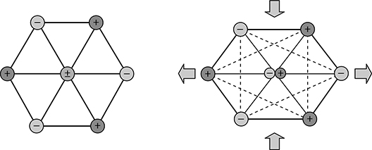
FIGURE 8.2 Deformation of a piezoelectric crystal. Asymmetry of electric charge causes polarization and electric output.
Piezoelectricity originated from the charge asymmetry in dielectric crystals. Deformation of a piezoelectric material generates an electric dipole in a unit cell of the crystal, and summation of individual dipoles becomes polarization, which is converted to the electric output (Figure 8.2). Piezoelectricity has two characteristics: One is the piezoelectric effect, which means the charge generation by external stress or strain, and the other is the inverse piezoelectric effect, which is force generation by an external electric field. These characteristics imply that the piezoelectric materials are inherently sensors and actuators. Therefore, if we integrate piezoelectric materials into MEMS, microsensors or actuators are easily developed, especially in simple microstructures.
8.1.2 Piezoelectric Thin Films
For integration of piezoelectric materials into MEMS, the piezoelectric materials should be prepared in thin-film form. The most popular piezoelectric material is Pb(Zr,Ti)O3 (PZT) because of its excellent energy conversion efficiency between mechanical and electrical domains. The deposition and characterization of PZT thin films have been intensively studied; recently, some piezoelectric MEMS composed of PZT films have been developed as commercial products.
In the case of energy harvesters, the piezoelectric property is one of the most important factors to determine power generation efficiency from environmental vibration, and PZT thin films are commonly applied to small-scale vibration generators. However, issues still remain: deposition of the well-crystallized piezoelectric films with complex composition and precise measurement of piezoelectric properties of thin films. In addition, PZT contains toxic lead, which would be an issue for the environment and human health.
In this chapter, the deposition process of PZT thin films is described from the viewpoint of MEMS applications. In addition, the recent progress of the lead-free piezoelectric thin films is introduced. Among a variety of piezoelectric MEMS, we pick up the piezoelectric MEMS energy harvesters, and the basic characteristics and applications of piezoelectric MEMS energy harvesters are presented.
8.2 Preparation of Piezoelectric Pzt Thin Films
8.2.1 Deposition of Pzt Thin Films for Mems
TABLE 8.1 Pzt deposition Process in MeMs
| Process | Advantage | Disadvantage |
| CSD | Low cost | Multiple coating |
| CVD | Uniform coverage | Cost of source material |
| PLD | Reproducibility of target composition | Small area |
| Sputter | Fast deposition rate | Cost of apparatus |
For the deposition of the piezoelectric materials, especially PZT-based perovskite thin films, several deposition techniques have been studied: chemical solution deposition (CSD; sol-gel deposition) [1], chemical vapor deposition (CVD) [2], pulsed laser deposition (PLD) [3], and sputtering [4]. These four methods can produce well-crystallized PZT thin films; however, each of them has advantages and disadvantages from the viewpoint of piezoelectric MEMS, as shown in Table 8.1. Among these methods, CSD is one of the popular techniques to prepare piezoelectric PZT thin films because it does not need expensive deposition apparatus. However, multiple spin-coating and baking processes are necessary to obtain a thickness of more than 1 μm, which often causes composition variation along the thickness and reduction of piezoelectric properties [5].
On the other hand, CVD is another candidate for high-quality PZT deposition. The advantage of this method is excellent step coverage, which is useful for semiconductor memories (FeRAM). However, because the source materials of PZT are expensive compared to the other methods, it is not suitable for the deposition of micron-thick piezoelectric PZT films in piezoelectric MEMS. PLD is also a popular method for PZT deposition; however, the deposition area with uniform thickness in a Si wafer is usually small and it is difficult to fabricate piezoelectric MEMS devices as commercial products.
For the PZT deposition in piezoelectric MEMS, radio frequency (RF)-magnetron sputtering is a practical method to produce micron-thick PZT films in a single deposition at lower cost. Sputtering deposition enables PZT films to be formed on a variety of substrates with high deposition rates of more than 1 μm/ h. On the other hand, sputtering deposition synthesizes the films in a nonthermal equilibrium condition; the deposited PZT thin films show unique characteristics that the PZT thin films of CSD or CVD do not have. For example, sputtered PZT thin films usually contain excess Pb, which is located not in A site but in B site [6,7]. Furthermore, the sputtered PZT thin films have stable initial poling from bottom to surface, and this phenomenon is useful from the viewpoint of long-term duration of the piezoelectric MEMS sensors [4,8]. Sputtering deposition of the piezoelectric PZT thin films has already been used in mass production, such as ink-jet printer heads and gyro sensors [9].
8.2.2 Sputtering Deposition
TABLE 8.2 Sputtering Condition of Pzt

The RF-magnetron sputtering is a useful deposition technique, especially for the thin films composed of complex chemical composition. Typical sputtering conditions of the PZT thin films are listed in Table 8.2. The sputtering is performed under an Ar/ O2 mixed gas atmosphere of 0.3 ~ 0.5 Pa, where the substrates were heated up to around 600°C to grow the PZT films with perovskite structure. Postannealing with the temperature around 600°C is also effective to crystallize PZT films deposited at low substrate temperature. However, postannealing often involves fatal damage, such as cracking or peeling of the films, especially for the thick PZT films due to large thermal stress from the substrate.
Sintered ceramics are usually used as target materials to stabilize film composition. It is well known that the morphotropic phase boundary (MPB) exists at a Zr:Ti ratio of 52:48, where dielectric and piezoelectric properties exhibit maxima. Therefore, the PZT ceramic target with MPB composition is usually used for the piezoelectric PZT films. Furthermore, since Pb and PbO are easily re-evaporated from the deposited films, excess PbO was often added in the target to maintain stoichiometory of the PZT films. Stabilization of Pb is an important factor to obtain the PZT thin films with perovskite structure, and depletion of Pb usually causes a pyrochlore phase in the deposited films. On the other hand, excess Pb is thought to be settled in B site of the perovskite, and it does not cause the serious degradation of the electric properties of the sputtered PZT thin films [6,7].
8.2.3 Crystal Structure of Pzt Thin Filmsl
Piezoelectricity is originated from asymmetry of the crystal structure, which strongly influences piezoelectric properties. Usually, PZT films are grown on Pt-coated Si substrates with a Ti adhesive layer at the interface of Si. The x-ray diffraction (XRD) patterns of the PZT films deposited on Pt/ Ti/ SiO2/Si substrates are shown in Figure 8.3. The clear diffraction peaks from perovskite PZT is observed without the other phases such as pyrochlore. On the other hand, the preferential orientation of the PZT can be controlled by optimization of the sputtering conditions. Especially, a seed layer such as (Pb, La)TiO3 (PLT) or SrRuO3 (SRO) is effective in ensuing perovskite growth and orientation control in PZT sputtering [10–12].

FIGURE 8.3 XRD patterns of PZT thin films on Pt/ Ti/ Si substrates by RF-magnetron sputtering.
The preferential orientation of the piezoelectric thin films is one of the determining factors of the piezoelectric properties for piezoelectric thin films. Although PZT thin films on Si substrates usually have polycrystalline structure, epitaxial substrates such as MgO and SrTiO3 enable epitaxial growth of PZT films by RF-sputtering, PLD, or CVD. Epitaxial substrates can control orientation and domain structure of the PZT films so that the electric properties including piezoelectricity can be enhanced by perfect alignment of the polar direction. Recently, Pb-based piezoelectric thin films have been grown on Si substrates by using a multilayered buffer such as SrTiO3/MgO/ TiN or SrRuO3/SrTiO3. Baek et al. reported that Pb(Mg1/3Nb2/3) O3-PbTiO3 ( PMN-PT) thin films were grown on miscut Si substrates with multi-buffer layers by off-axis sputtering deposition, and large piezoelectric properties could be obtained [13]. The epitaxial piezoelectric thin films of PZT or PMN-PT are ideal materials for piezoelectric MEMS; however, the sputtering conditions are very sensitive to the epitaxial growth of the piezoelectric films including buffer layers, and the polycrystalline thin films with preferred c-axis orientation are usually used for the practical applications.
8.2.4 Evaluation of Piezoelectric Properties for Thin Films
Since the piezoelectric films are deposited on substrates, the piezoelectric effect of the thin film is strongly suppressed by the existence of the substrate, and it makes it difficult to measure the precise piezoelectric properties. Several measurement methods have been used to determine piezoelectric coefficient of the thin films [14]. One of the most popular methods is the measurement of the thickness change originated from the longitudinal piezoelectric effect using an atomic force microscope (AFM) or laser interferometer [15,16]. Although this method offers ease of measurement of the effective longitudinal piezoelectric strain, the transverse piezoelectric coefficient, which is indispensable for the device design of piezoelectric MEMS, cannot be obtained.
The most practical method to evaluate transverse piezoelectric properties of thin films is the measurements of piezoelectric cantilevers. The piezoelectric properties of d-and e-forms are expressed as the following equations:
where
k = 1, 2, 3
i, j = 1, 2, 3, 4, 5, 6
Ti, Sj, and Ek are the stress, strain, and electric field components
cijE and sijE are constant-electric-field elastic stiffness components and elastic compliance components
eki and dki are piezoelectric coefficients
In order to evaluate transverse piezoelectric properties (d31 or e31) of thin films, unimorph cantilevers are often used as specimens. Unimorphs are composed of double layers of piezoelectric and nonpiezoelectric materials, and most piezoelectric MEMS sensors or actuators have these structure. Output of a unimorph is determined by transverse piezoelectric properties; for example, tip displacement of the unimorph actuator is calculated by the following equation:
Here, h, s11, L, V, and δ are the thickness, the elastic compliance, the length of the cantilever, the applied voltage, and the tip displacement, respectively [17]. The subscripts s and p denote the substrate and the PZT thin film, respectively. If the dimension and mechanical properties of the unimorphs are known, the transverse piezoelectric coefficient d31 is obtained from Equation (8.3). Especially in the case in which the thickness of a substrate is much larger than that of a piezoelectric thin film, trans-verse piezoelectric coefficient d31 can be approximated as
The mechanical properties of the thin films usually depend on the deposition process and the substrate. Therefore, it is inevitable to measure the elastic properties of the PZT thin films precisely to obtain transverse piezoelectric coefficient d31, although they are difficult to evaluate.
On the other hand, in the case of a piezoelectric thin film on the substrate, the effects of plane and shear strains can be neglected. If an external electric field is applied to a unimorph actuator, two-dimensional in-plain strain is generated and the transverse piezoelectric coefficient e31 is written as
The effective transverse piezoelectric coefficient e31,f is defined as e31,f = d31/ (s11E + s12E) [18], and then Equation (8.5) is expressed as
The effective transverse piezoelectric coefficient was defined to eliminate the ambiguous mechanical properties of the thin films, and the following coefficient can be determined from the displacement of a unimorph cantilever:
Here, Es, νs are Young’s modulus and the Poisson ratio of substrate [19,20]. The effective transverse piezoelectric coefficient e31,f or e31* can be easily obtained from the tip displacement of a unimorph cantilever and it is useful to evaluate the trans-verse piezoelectric property as a kind of figure of merit.
8.3 Lead-Free Piezoelectric Thin Films
From the viewpoint of environmental impact of piezoelectric materials and devices, lead-free piezoelectric materials have been strongly demanded. Recently, a variety of lead-free piezoelectric materials has been studied and some of them show large piezoelectric properties comparable with PZT ceramics [21,22]. Typical lead-free piezoelectric materials are listed in Table 8.3. The studies on Ba, Bi, and alkali-based perovskite materials exhibited relatively large piezoelectric properties. Recently, it has been reported that the (K1Na) NbO3 (KNN)-based piezoelectric ceramics, whose crystal orientation and additives are optimized, show a large piezoelectric coefficient and high Curie temperature that are comparable with PZT [26]. This discovery boosted the research of lead-free piezoelectrics.
In order to integrate lead-free piezoelectric materials into MEMS, a variety of lead-free piezoelectric ceramics has been prepared on Si substrates in the thin-film form. The most promising lead-free piezoelectric thin films are KNN thin films. Just like PZT thin films, KNN thin films can be deposited by several deposition processes, such as RF-sputtering [27,28], CVD [29], and PLD [30,31]. In the case of KNN thin films, RF-magnetron sputtering can produce high-quality thin films and the sputtering conditions are almost the same as those of PZT. Shibata et al. reported successfully fabricating the KNN thin films by RF-magnetron sputtering and confirmed excellent piezoelectric properties compatible with PZT [32,33].
TABLE 8.3 Piezoelectric Properties of Typical Lead-Free Piezoelectric Ceramics

8.3.1 Piezoelectric Properties of Knn Thin Films
The transverse piezoelectric properties were evaluated from the tip displacement of unimorph cantilevers, and the transverse piezoelectric coefficient e31,f is calculated by Equation (8.8). To examine the piezoelectric characteristics of the sputtering-deposited KNN thin films, e31,f was compared with that of PZT thin films. First, the KNN and PZT thin films were deposited on Si substrates (200 μm). The thickness of the KNN and PZT thin films was 3 and 2 μm, respectively. The film composition of both films was close to MPB composition (KNN: K/ Na = 45/55, PZT: Zr/ Ti = 50/50). XRD patterns of the KNN and PZT thin films are shown in Figure 8.4. The KNN film shows a preferential orientation of (001) in a perovskite unit cell. On the other hand, the PZT film shows relatively random orientation with strong diffractions of (001) and (110). The cross-sectional SEM (scanning electron microscopy) images of KNN and PZT films are shown in Figure 8.5. Both films have very dense structure without pores or cavities at the interface of the substrates, implying that the films strongly adhered to the substrates.
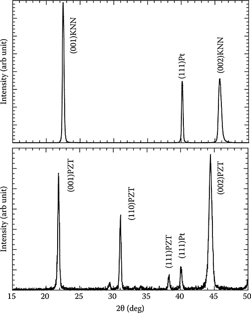
FIGURE 8.4 XRD patterns of KNN and PZT thin films deposited on Pt/ Ti/ Si substrates.

FIGURE 8.5 Cross-sectional SEM images of KNN and PZT thin films deposited on Pt/ Ti/ Si substrates.
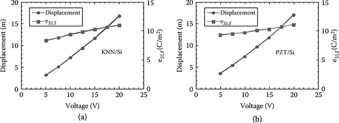
FIGURE 8.6 Displacement and calculated e31,f as a function of applied voltage; (a) KNN/ Si and (b) PZT/ Si.
The KNN and PZT films on Si substrates were cut into beam shape (width of
3.4 mm, length of 20 mm), and one end of each beam was clamped in a vise so as to create a simple unimorph cantilever (length of 16.5 mm for KNN/ Si, 17.5 mm for PZT/ Si). The piezoelectric coefficient e31,f was calculated from the tip displacement by applied voltages in the range of 5–20 V. Results for the KNN and PZT films, respectively, are e31,f = −8.4 to −11.0 C/ m2 and −9.3 to −11.1 C/ m2, as shown in Figure 8.6. Thus, the piezoelectric properties of KNN thin film are comparable to those of PZT thin film.
8.3.2 Microfabrication of Knn Thin Films
At present, piezoelectric MEMS devices are usually made of PZT thin films, and the PZT thin films are fabricated into a variety of microstructures by wet or dry etching processes [4,34,35]. Although the microfabrication process of PZT-based thin films has been established, there are few reports on the microfabrication of lead-free piezoelectric thin films. In the case of KNN thin films, effective wet-and dry-etching methods have not been established so far because KNN is stable for acid or alkaline. Kurokawa et al. reported that the KNN thin film was microfabricated into a microcantilever by reactive ion etching (RIE) with Ar/ C4F8 mixed gas and evaluated etching characteristics of KNN thin film [36]. Microfabrication of KNN thin film was conducted by magnetic neutral loop discharge (NLD) RIE, which could produce uniform and high-density plasma at low pressure and low electron temperature [15]. The etching gas flow rate of Ar/ C4F8 was 50/2.5 standard cubic centimeters per minute (SCCM) under the pressure of 0.15 Pa; the antenna power of 800 W and bias power of 250 W were applied for 35 min. A Cr metal mask was used because conventional photoresist could not sustain high-density plasma etching. Figure 8.7 shows the KNN thin films on a Si substrate after NLD-RIE etching. KNN thin films were successfully etched into a cantilever-shaped structure. Then, cantilevers were released by Si deep-RIE (DRIE), and the SEM image of the resulting KNN micro-cantilevers is shown in Figure 8.8. Although the cantilevers were strongly bent by the asymmetric internal stress of KNN thin films and electrodes, they showed clear ferroelectric and piezoelectric properties.
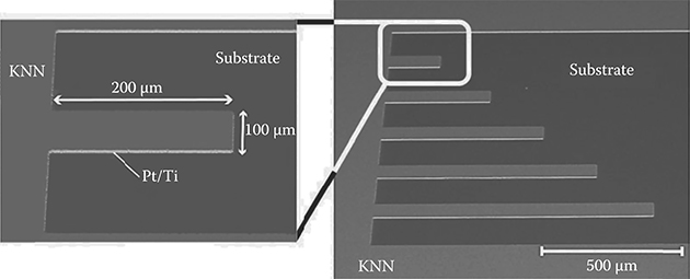
FIGURE 8.7 SEM image of microfabricated KNN thin films on Pt/ Ti/ Si substrate.
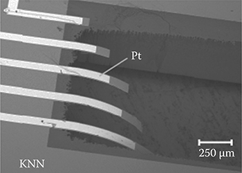
FIGURE 8.8 SEM image of KNN microcantilevers released from Si substrate by DRIE.
8.4 Vibration Energy Harvesters
8.4.1 Piezoelectric Mems Energy Harvesters
Recently, vibration energy harvesting technologies have attracted considerable attention as an energy source for microdevices, especially for autonomous wireless sensor nodes [37–39]. Vibration MEMS energy harvesters (EHs) can be long-life, maintenance-free electric power sources to replace primary batteries. As vibrational energy widely exists in the environment, it is therefore useful in areas where solar power cannot be used. It is reported that the sensor nodes can be operated by small power of about tens to hundreds of microwatts [6]; however, the generated power is still insufficient and improvements in efficiency are strongly demanded.
Vibration generators are generally classified into three types: electromagnetic, electrostatic, and piezoelectric systems. Among them, piezoelectric power generators show the highest power density [37]. Furthermore, because piezoelectric energy harvesters have simple cantilever structures, integration with MEMS processing is not difficult. Piezoelectric MEMS EHs are usually unimorph cantilever structures constructed from piezoelectric PZT thin films on Si substrates. Because the vibration amplitude of the cantilever is maximized at its resonance frequency, the resonance frequency of the cantilevers should be adjusted to environmental vibrations.
However, conventional MEMS EHs have a higher resonance frequency of more than 1 kHz because of the small size of the resonators, although the frequency of environmental vibrations is generally less than 200 Hz [40]. Furthermore, PZT/ Si unimorph cantilevers are brittle materials and the output power is restricted by the fracture strength of the cantilever under large vibration. Another challenge is the lead-free piezoelectric energy harvesters. Among a variety of piezoelectric MEMS EHs, PZT thin films are the most popular piezoelectric materials. On the other hand, as described in a previous section, KNN thin films have been investigated for use in lead-free piezoelectric MEMS, and piezoelectric MEMS EHs of lead-free thin films are strongly desired.
Piezoelectric MEMS EHs of piezoelectric thin films are described in this chapter. First, the power generation performance of simple lead-free KNN thin-film EHs is compared with the PZT thin-film EHs. Next, we present the metal-based piezoelectric MEMS EHs. The PZT thin films were directly deposited on the microfabricated stainless steel cantilevers by RF-magnetron sputtering and fabricated vibration EHs not only for a simple, low-cost fabrication, but also for a long lifetime of robust piezoelectric cantilevers.
8.4.2 Power Generation of Pzt and Knn Thin Films
Power generation performances of KNN and PZT thin films were evaluated. To simplify the characterization, simple unimorph cantilevers of KNN and PZT thin films without seismic mass were used for measurements. The samples were the same cantilevers used in Section 8.3.1, and the transverse piezoelectric coefficient e31,f of KNN and PZT thin films was around −10 C/ m2. The relative dielectric constants (εr) of the KNN and PZT films were 744 and 872, and the dielectric losses (tan δ) were 7.1% and 3.9%, respectively. The power generation efficiency of the piezoelectric thin films can be evaluated by the figure of merit (FOM) from the following equation [13]:
FOM represents the electromechanical coupling factor of the thin film materials. Because piezoelectric and dielectric properties of the KNN and PZT films are almost the same, their FOM is calculated to be around 15 GPa. This result indicates that the lead-free KNN thin films have a comparable power-generation performance to that of PZT thin films.
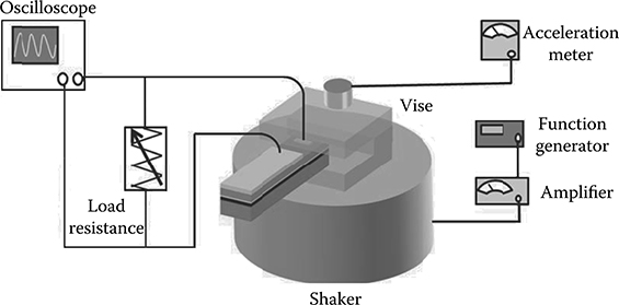
FIGURE 8.9 Measurement setup of piezoelectric energy harvesters.
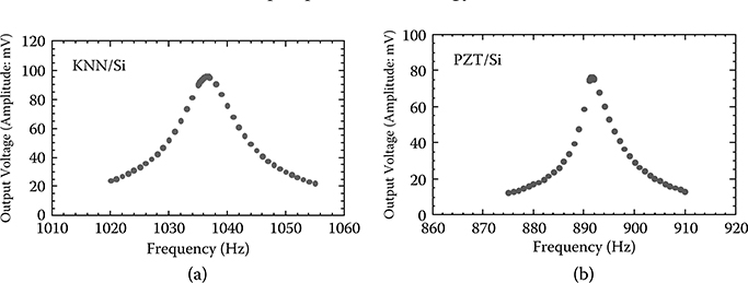
FIGURE 8.10 Frequency response of output voltage; (a) KNN/ Si, and (b) PZT/ Si unimorph EHs.
Output power of each unimorph cantilever was measured using the setup shown in Figure 8.9. The cantilever was mounted on a shaker and connected lead lines between the top and bottom electrodes to load resistance. Then, the output voltage was measured under the continuous vibration. The frequency response of output voltage is shown in Figure 8.10. The output voltage (for acceleration 10 m/ s2, load resistance R = 1 MΩ) showed clear peaks at frequencies of 1036 and 892 Hz and the quality factor Q was 120 and 160 for the KNN and PZT cantilevers, respectively. Figure 8.11 shows the average output power P = V/(2R) as a function of load resistance for KNN and PZT EHs. Measurements were performed at the resonance frequency of each cantilever and the acceleration of 10 m/s2. Peak output power for the KNN and PZT films was 1.1 μλ¥ at 1.7 kQ and 1.0 μν at 1.2 kQ, respectively. Thus, the lead-free KNN film performs comparably to the PZT film with respect to power generation.
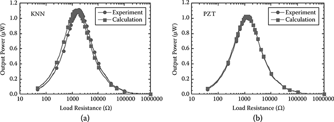
FIGURE 8.11 Output power as a function of load resistance; (a) KNN/Si, and (b) PZT/Si unimorph EHs.
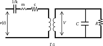
FIGURE 8.12 Illustration of equivalent electric circuit of piezoelectric EH.
The power generation for the piezoelectric EHs can be characterized by considering the equivalent electric circuit [41]. The mechanical and electrical circuit model is illustrated in Figure 8.12. The mechanical vibration of the EHs is simplified in a lumped model, as shown in Figure 8.13, and the motion equation is
where m, c, and k are mass, damping coefficient, and spring constant, and z and y are relative displacement of mass and the displacement of the base. If the conversion ratio between electric potential (V) and mechanical force (F) is Γ, Equation (8.10) can be expressed as
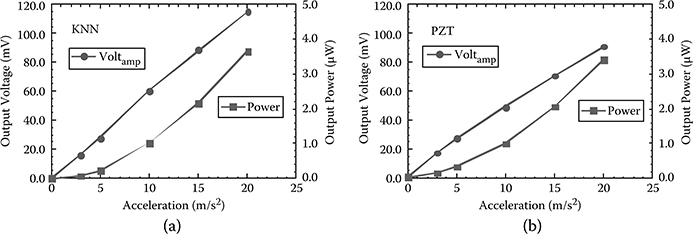
FIGURE 8.13 Output voltage and electric power of (a) KNN and (b) PZT EHs as a function of acceleration.
Then, the output voltage is expressed as the following equation:
where m, a, ω0, C, R, and Q are the cantilever’s effective mass, acceleration, fundamental mechanical angular frequency, capacitance, load resistance, and mechanical quality factor. K represents the generalized electromechanical coupling (GEMC) factor. The averaged output power is obtained as
Maximum output power is obtained when the EHs are shaken at the resonance frequency, and Equation (8.11) can be simplified as
where μ1 (= 1.566) is the correction factor for simple cantilever vibration at the first resonance [42]. The optimal load resistance Ropt is obtained from the differentiation of Equation (8.14) by R, and the maximum output power Popt is obtained at Ropt; they are expressed as
This equation implies that, if mechanical and electrical values are given, output power can be determined by K and Q. The GEMC factor, an important parameter for determining the output power of piezoelectric energy harvesters, is obtained from
where ωshort and ωopen are the resonance angular frequencies of the associated short and open circuits, respectively.
The energy harvesters were plotted in Figure 8.11 and calculated the output power for the KNN/ Si and PZT/ Si energy harvesters in the case of K2 = 1.7 × 10⁻³ and 0.65 × 10⁻³, respectively. The maximum output power and K2 are higher for KNN/ Si than for PZT/ Si. The performance of KNN thin-film EHs is comparable to or better than that of PZT thin-film EHs. The acceleration dependence of the output power was measured with accelerations ranging from 1 to 20 m/s2 with the optimal load resistance, and the results are shown in Figure 8.13. For both EHs, the output voltage proportionally increases, while output power increases with the square of the acceleration, respectively. These results almost follow the theoretical prediction. The KNN and PZT EHs generated stable electric power under the high acceleration to 20 m/ s2 and it reached 3.7 and 3.4 μW at 20 m/ s2, respectively.
Because we used simple unimorph structures to evaluate the fundamental characteristics of the films, our observed output power and GEMC factors are smaller than those of other piezoelectric MEMS energy harvesters reported to date. However, the output power of both types of EHs can easily be enhanced by attaching a seismic mass to the cantilever tip and by further optimizing the harvester design and structure.
8.4.3 Metal-Based Piezoelectric Mems Energy Harvesters
Piezoelectric MEMS EHs of metal cantilevers are advantageous to the long-term stability of the power generation due to excellent toughness of the metal. Furthermore, strong toughness of the metal cantilevers enables the reduction of the thickness of the cantilever and heavy tip mass attachment, which lead to the reduction of the resonant frequency and enhancement of vibration. In this study, PZT thin films were directly deposited on stainless steel cantilevers of ferritic stainless steel (SS430) cantilevers. The coefficients of thermal expansion (CTE) for SS430 and PZT are about 11.4 × 10⁻⁶ K–1 and 9 × 10⁻⁶ K–1, respectively. Considering that the CTE of typical austenitic stainless steel (SS304) is 18.4 × 10⁻⁶ K–1, the small difference in CTE between PZT and SS430 is expected to mitigate the initial bending of the unimorph cantilevers. The fabrication process is shown in Figures 8.14 and 8.15. First, 30-μm thick SS430 cantilevers with tip masses were fabricated from a 300-μm thick stainless steel plate in a two-step, double-sided spray etching process using ferric chloride solution. This etching process enables fabrication of the fixed end and the tip mass of cantilevers without bonding or clamping. With the cantilever length fixed at 7.5 mm, cantilevers of different widths of 1.0, 2.0, and 5.0 mm were constructed, while the built-in tip mass varied from 5.0 to 25 mg.
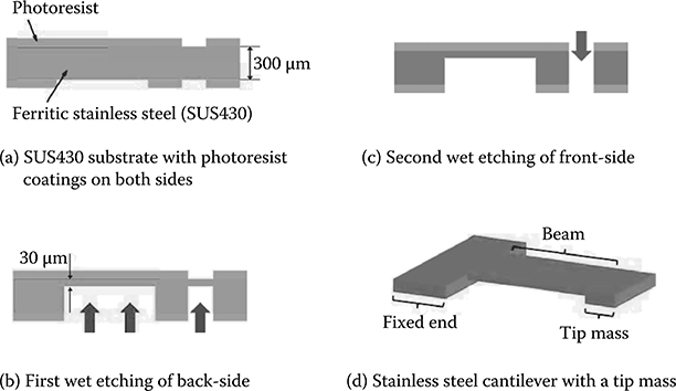
FIGURE 8.14 Fabrication process of the stainless steel cantilevers with a tip mass by two-step spray etching.
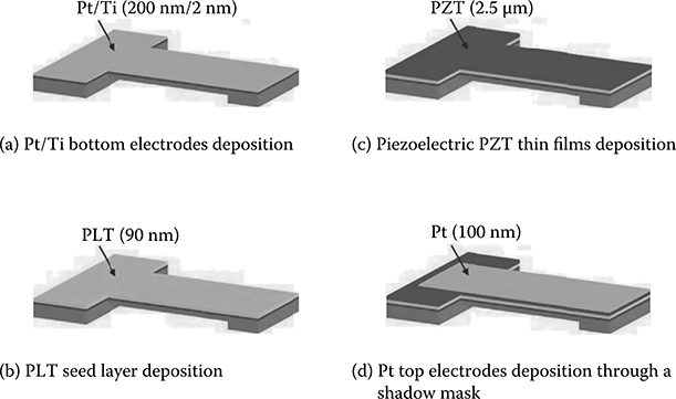
FIGURE 8.15 Sputtering deposition of the piezoelectric PZT thin films on microfabricated stainless steel cantilever.
Prior to PZT deposition, Pt/ Ti bottom electrodes were deposited by RF-magnetron sputtering onto the microfabricated cantilevers. A (Pb, La)TiO3 (PLT) seed layer was deposited to promote the growth of the PZT thin films, and successively the PZT thin films with composition Zr/ Ti = 53/47 were deposited also by RF-magnetron sputtering [43,44]. The substrate was heated to around 600°C, and deposition was performed under a mixed gas atmosphere of Ar/ O2 with a flow of 9.0/1.0 SCCM. The thickness of the PZT films was 2.5 μm. The Pt top electrodes were prepared through a shadow mask. Direct deposition of the PZT thin films on the microfabricated cantilever could drastically simplify fabrication of the piezoelectric MEMS EHs. Figure 8.16 shows the image of the piezoelectric EHs of the PZT thin film on a stainless steel cantilever.
The relative dielectric constant εr and dielectric loss tan δ of the PZT films were 325−445 and 2.1%−3.3%, respectively. The low relative dielectric constant of PZT films is caused by in-plane compressive stress due to the difference in CTE between PZT thin films and stainless steel. The transverse piezoelectric properties of PZT films were measured from the deflection of the unimorph cantilevers, and e31,f was calculated to be about –4.0 C/ m2.

FIGURE 8.16 Photograph of piezoelectric EH of PZT thin film on microfabricated stainless steel cantilevers.
Figure 8.17 shows the frequency response of output voltage of a unimorph cantilever (7.5 mm long, 5.0 mm wide, 25 mg tip mass) at the acceleration of 10 m/ s2. A clear peak of the output voltage appeared at a resonance frequency of 367 Hz. The Q value was calculated to be 80 from the half-power bandwidth method. As shown in Figure 8.17, the nonlinear response (jump phenomenon and hysteresis) was clearly observed arising from softening spring effects; however, it is preferable in expanding the range of resonance frequency. Figure 8.18 shows the output power and the output voltage as a function of load resistance. The measurement was performed at the resonance frequency of 367 Hz under the acceleration of 10 m/ s2. The averaged output power [P = V2/2R] reached 6.8 μW at the optimum load resistance of 10 kΩ. We define the power density as the maximum output power divided by the volume of the cantilever; the power density of design 1 is 1.7 mW/ cm3. GEMC K2 of the PZT films on stainless steel cantilever was calculated to be 2.8 × 10⁻³ and almost independent of the design of the unimorph cantilevers. Compared with K2 for PZT films on Si cantilevers (0.65 × 10⁻³), we achieved an extremely high conversion efficiency for our PZT energy harvesters on stainless steel cantilevers.
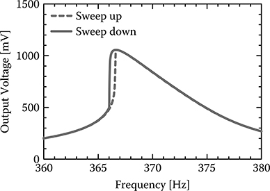
FIGURE 8.17 Frequency response of piezoelectric EH of PZT thin film on stainless steel cantilever.

FIGURE 8.18 Output voltage and generated power as a function of load resistance.
8.5 Summary
In this chapter, the outline of piezoelectric MEMS technologies is presented. Ferroelectric materials have a variety of functionality, including piezoelectricity, and integration of piezoelectric materials on MEMS enhances the function of the devices even in the simple microstructures. For the development of piezoelectric MEMS, deposition, evaluation, and microfabrication of piezoelectric thin films should be established. PZT is the most popular piezoelectric material, and PZT thin films with a thickness of a few microns are used for the MEMS applications. RF-magnetron sputtering is a suitable method for the deposition of piezoelectric PZT films. Transverse piezoelectric properties of the thin films are indispensable to design the piezoelectric MEMS, and they can be evaluated from the actuator properties of unimorph cantilevers of a PZT film and a substrate. On the other hand, lead-free piezoelectric thin films have been investigated as environmentally friendly materials, and it was reported that KNN thin films show large piezoelectric properties almost compatible with those of PZT films. Among a variety of piezoelectric MEMS applications, MEMS EHs have attracted attention for acting as an autonomous energy source for microdevices, especially for wireless sensor nodes. For the practical application, robust, environmentally friendly, low-cost, and high-efficiency MEMS EHs are required. Progress of the piezoelectric thin-film technologies will be a key to solving these issues.
Reference
1. B. Piekarski, M. Dubey, E. Zakar, R. Polcawich, D. DeVoe, and D. Wickenden. 2002. Sol-gel PZT for MEMS applications. Integrated Ferroelectrics 42:25–37.
2. C. M. Foster, G. R. Bai, R. Csencsits, J. Vetrone, R. Jammy, L. A. Wills, E. Carr, and J. Amano. 1997. Single-crystal Pb(Zrx,Ti1–x)O3 thin films prepared by metal– organic chemical vapor deposition: Systematic compositional variation of electronic and optical properties. Journal of Applied Physics 81:2349–2357.
3. I. Vrejoiu, G. Le Rhun, L. Pintilie, D. Hesse, M. Alexe, and U. Gösele. 2006. Intrinsic ferroelectric properties of strained tetragonal PbZr0.2Ti0.8O3 obtained on layer-by-layer grown, defect-free single-crystalline films. Advanced Materials 18:1657–1661.
4. I. Kanno, S. Fujii, T. Kamada, and R. Takayama. 1997. Piezoelectric properties of c-axis oriented Pb(Zr,Ti)O3 thin films. Applied Physics Letters 70:1378–1380.
5. F. Calame, and P. Muralt. 2007. Growth and properties of gradient free sol-gel lead zirconate titanate thin films. Applied Physics Letters 90:062907.
6. T. Matsunaga, T. Hosokawa, Y. Umetani, R. Takayama, and I. Kanno. 2002. Structural investigation of Pby(Zr0.57Ti0.43)2–yO3 films deposited on Pt(001)/MgO(001) substrates by RF sputtering. Physics Review B 66:064102.
7. I. Kanno, H. Kotera, T. Matsunaga, and K. Wasa. 2005. Intrinsic crystalline structure of epitaxial Pb(Zr,Ti)O3 thin films, Journal of Applied Physics 97:074101.
8. J. F. Shepard, Jr., F. Chu, I. Kanno, and S. T. McKinstry. 1999. Characterization and aging response of the d31 piezoelectric coefficient of lead zirconate titanate thin films. Journal of Applied Physics 85:6711–6716.
9. E. Fujii et al. 2007. Preparation of (001)-oriented Pb(Zr,Ti)O3 thin films and their piezoelectric applications. IEEE Transactions on Ultrasonics Ferroelectrics Frequency Control 54:2431–2438.
10. I. Kanno, S. Hayashi, T. Kamada, M. Kitagawa, and T. Hirao. 1993. Low-temperature preparation of Pb(Zr,Ti)O3 thin films on (Pb,La)TiO3 buffer layer by multi-ion-beam sputtering. Japanese Journal of Applied Physics 32:4057–4060.
11. T. Morimoto, O. Hidaka, K. Yamakawa, O. Arisumi, H. Kanaya, T. Iwamoto, Y. Kumura, I. Kunishima, and S. Tanaka. 2000. Ferroelectric properties of Pb(Zi, Ti)O3 capacitor with thin SrRuO3 films within both electrodes. Japanese Journal of Applied Physics 39:2110–2113.
12. K. Tomioka, F. Kurokawa, R. Yokokawa, H. Kotera, K. Adachi, I. Kanno. 2012. Composition dependence of piezoelectric properties of pb(zr,ti)o3 films prepared by combinatorial sputtering, Japanese Journal of Applied Physics 51:09LA12.
13. S. H. Baek et al. 2011. Giant piezoelectricity on Si for hyperactive MEMS. Science 334:958.
14. J.-M. Liu, B. Pan, H. L. W. Chan, S. N. Zhu, Y. Y. Zhu, and Z. G. Liu. 2002. Piezoelectric coefficient measurement of piezoelectric thin films: An overview. Materials Chemistry and Physics 75:12–18.
15. G. Zavala, J. H. Fendler, and S. T. McKinstry. 1997. Characterization of ferroelectric lead zirconate titanate films by scanning force microscopy. Journal of Applied Physics 81:7480–7491.
16. A. L. Kholkin, C. Wutchrich, D. V. Taylor, and N. Setter. 1996. Interferometric measurements of electric field-induced displacements in piezoelectric thin films. Review of Scientific Instruments 67:1935–1941.
17. J. G. Smits, and W. Choi. 1991. The constituent equations of piezoelectric heterogeneous bimorphs. IEEE Transactions on Ultrasonics Ferroelectronics Frequency Control 38:256–270.
18. M. A. Dubois, and P. Muralt. 1999. Measurement of the effective transverse piezoelectric coefficient e31,f of AlN and Pb(Zrx,Ti1–x)O3 thin films. Sensors and Actuators A 77:106–112.
19. I. Kanno, H. Kotera, and K. Wasa. 2003. Measurement of transverse piezoelectric properties of PZT thin films. Sensors and Actuators A 107:68–74.
20. D.-M. Chun, M. Sato, and I. Kanno. 2013. Precise measurement of the transverse piezoelectric coefficient for thin films on anisotropic substrate. Journal of Applied Physics 113:044111.
21. T. Takenaka, H. Nagata, and Y. Hiruma. 2007. Current developments and prospective of lead-free piezoelectric ceramics. Japanese Journal of Applied Physics 47:3787–3801.
22. P. K. Panda. 2009. Review: Environmental friendly lead-free piezoelectric materials. Journal of Materials Science 44:5049–5062.
23. T. Takenaka, K. Maruyama, and K. Sakata. 1991. (Bi1/2Na1/2)TiO3-BaTiO3 system for lead-free piezoelectric ceramics. Japanese Journal of Applied Physics 30:2236–2239.
24. L. Egerton, and D. M. Dillon. 1959. Piezoelectric and dielectric properties of ceramics in the system potassium-sodium niobate. Journal of American Ceramics Society 42:438–442.
25. W. Liu, and X. Ren. 2009. Large piezoelectric effect in Pb-free ceramics. Physics Review Letters 103:257602.
26. Y. Saito, H. Takao, T. Tani, T. Nonoyama, K. Takatori, T. Homma, T. Nagaya, and M. Nakamura. 2004. Lead-free piezoceramics. Nature 432:84–87.
27. T. Mino, S. Kuwajima, T. Suzuki, I. Kanno, H. Kotera, and K. Wasa. 2007. Piezoelectric properties of epitaxial NaNbO3 thin films deposited on (001)SrRuO3/Pt/MgO substrates. Japanese Journal of Applied Physics 46:6960–6963.
28. I. Kanno, T. Mino, S. Kuwajima, T. Suzuki, H. Kotera, and K. Wasa. 2007. Piezoelectric properties of (K,Na)NbO3 thin films deposited on (001)SrRuO3/Pt/MgO substrates. IEEE Transactions on Ultrasonics, Ferroelectrics, Frequency Control 54:2562–2566.
29. A. Onoe, A. Yoshida, and K. Chikuma. 1996. Heteroepitaxial growth of KNbO3 single-crystal films on SrTiO3 by metalorganic chemical vapor deposition. Applied Physics Letters 69:167–169.
30. S. I. Khartsev, M. A. Grishin, and A. M. Grishin. 2005. Characterization of heteroepitaxial Na0.5K0.5NbO3/La0.5Sr0.5CoO3 electro-optical cell. Applied Physics Letters 86:062901.
31. T. Saito, T. Wada, H. Adachi, and I. Kanno. 2004. Pulsed laser deposition of high-quality (K,Na)NbO3 thin films on SrTiO3 substrate using high-density ceramic targets. Japanese Journal of Applied Physics 43:6627–6631.
32. K. Shibata, F. Oka, A. Ohishi, T. Mishima, and I. Kanno. 2008. Piezoelectric properties of (K,Na)NbO3 films deposited by RF magnetron sputtering. Applied Physics Express 1:11501.
33. K. Shibata, F. Oka, A. Nomoto, T. Mishima, and I. Kanno. 2008. Crystalline structure of highly piezoelectric (K,Na)NbO3 films deposited by RF magnetron sputtering. Japanese Journal of Applied Physics 47:8909–8913.
34. I. Kanno, Y. Tazawa, T. Suzuki, and H. Kotera. 2007. Piezoelectric unimorph miro-actuators with X-shaped structure composed of PZT thin films. Microsystems Technology 13:825–829.
35. Y. Kokaze, I. Kimura, M. Endo, M. Ueda, S. Kikuchi, Y. Nishioka, and K. Suu. 2007. Dry etching process for Pb(Zr,Ti)O3 thin-film actuators. Japanese Journal of Applied Physics 46:280–282.
36. F. Kurokawa, I. Kanno, R. Yokokawa, H. Kotera, F. Horikiri, K. Shibata, T. Mishima, and M. Sato. 2012. Microfabrication of lead-free (K,Na)NbO3 piezoelectric thin films by dry etching. Micro & Nano Letters 113:1223–1225.
37. S. Roundy, and P. K. Wright. 2004. A piezoelectric vibration based generator for wireless electronics. Smart Materials Structures 13:1131–1142.
38. S. P. Beeby, M. J. Tudor, and N. M. White. 2006. Energy harvesting vibration sources for microsystems applications. Measurement Science and Technology 17:R175–R195.
39. S-G. Kim, S. Priya, and I. Kanno. 2012. Piezoelectric MEMS for energy harvesting. MRS Bulletin 37:1039–1050.
40. S. Roundy, P. K. Wright, and J. Rabaey. 2003. A study of low level vibrations as a power source for wireless sensor nodes. Computer Communications 26:1131–1144.
41. M. Renaud, K. Karakaya, T. Sterken, P. Fiorini, C. Van Hoof, and R. Puers. 2008. Fabrication, modeling and characterization of MEMS piezoelectric vibration harvesters. Sensors and Actuators A 145–146:380–386.
42. A. Erturk, and D. J. Inman. 2008. On mechanical modeling of cantilevered piezoelectric vibration energy harvesters. Journal of Intelligent Material Systems and Structures 19:1311–1325.
43. T. Suzuki, I. Kanno, J. J. Loverich, H. Kotera, and K. Wasa. 2006. Characterization of Pb(Zr, Ti)O3 thin films deposited on stainless steel substrates by RF-magnetron sputtering for MEMS applications. Sensors and Actuators A 125:382–386.
44. K. Kanda, I. Kanno, H. Kotera, and K. Wasa. 2009. Simple fabrication of metal-based piezoelectric MEMS by direct deposition of Pb(Zr,Ti)O3 thin-films on titanium substrates. Journal of Microelectromechanical Systems 18:610–615.