
CHAPTER 8
Interfacing to the BeagleBone Buses
This chapter describes bus communication in detail, explaining and comparing the different bus types that are available on the BeagleBone. It describes how you can configure them for use, and how you can communicate with and control I2C, SPI, and UART devices, using both Linux tools and custom-developed C and C++ code. Practical examples are provided that use a low‐cost accelerometer, a serial shift register, and the Arduino microcontroller. After reading this chapter, you should have the skills necessary to interface the BeagleBone to almost all of its available bus types.
Equipment Required for This Chapter:
- BeagleBone Black (BBB)
- ADXL345 accelerometer on a breakout board
- 74HC595 shift register, LEDs, and resistors
- 3.3 V Arduino microcontroller or 5 V Arduino microcontroller and logic‐level translator
Further details on this equipment and chapter are available at www.exploringbeaglebone.com/chapter8/.
Introduction to Bus Communication
In Chapter 6, the use of GPIOs and analog I/O is discussed in detail, which makes it clear how you can connect the BBB to standalone components. This chapter examines more complex communications that can be performed using the bus interfaces that are available on the BBB. Bus communication is a mechanism that enables data to be transferred between the high‐level components of an embedded platform, using standardized communications protocols. The two most commonly used embedded systems buses are available on the BBB, and they are the subject of this chapter: Inter‐Integrated Circuit (I2C) and Serial Peripheral Interface (SPI). In addition, Universal Asynchronous Receiver/Transmitter (UART) devices are discussed. These are computer hardware devices that can be configured and used to send and receive serial data. When combined with appropriate driver interfaces, UARTs can implement standard serial communications protocols, such as RS‐232, RS‐422, or RS‐485.
Understanding the behavior and use of bus communications protocols and devices enables the possibility of building advanced BBB electronics systems. There are a huge number of complex sensors, actuators, input devices, I/O expanders, and other microcontrollers that conform to these communications protocols, and the BBB is capable of communicating with them all.
The topics discussed in this chapter are all demonstrated using practical examples of devices that were chosen based on their wide availability and low cost. However, the focus of this chapter is imparting an understanding of the techniques employed in using the BBB’s buses, rather than just describing the specific bus devices used. To this end, the chapter provides generic communications code that you can use in order to apply the principles described to any device of your choosing.
I2C
Inter‐Integrated Circuit (IIC or I2C) is a straightforward two‐wire bus that was designed by Philips in the 1980s to interface microprocessors or microcontrollers to low‐speed peripheral devices. A master device, such as the BBB, controls the bus, and many addressable slave devices can be attached to the same two wires. It has remained popular over the years, mainly due to its relative simplicity and breadth of adoption. It is currently used in smartphones, most microcontrollers, and even environmental management applications in large‐scale server farms. Here are some general features of the I2C bus:
- Only two signal lines are required for communication, the Serial Data (SDA) line for the bidirectional transmission of data, and the Serial Clock (SCL) line, which is used to synchronize the data transfer. Because the bus uses this synchronizing clock signal, the data transfer is said to be synchronous. The transmission is said to be bidirectional because the same SDA wire can be used for sending and receiving data.
- Each device on the bus can act as a master or a slave. The master device is the one that initiates communication and the slave device is the one that responds. Designated slave devices cannot initiate communication with the master device.
- Each slave device attached to the bus is pre‐assigned a unique address, which is in either 7‐bit or 10‐bit form. In the following example, 7‐bit addressing is used, i.e., 0x00 to 0x80 (27 = 12810 = 0x80).
- It has true multi‐master bus facilities, including collision detection and arbitration if two or more master devices activate at once.
- On‐chip noise filtering is built in as standard.
I2C Hardware
Figure 8-1(a) illustrates the interconnection of multiple slave devices to the I2C bus. All output connections to the SDA and SCL lines are in open‐drain configuration (discussed in Chapter 4), whereby all devices share a common ground connection. This means that devices with different logic families can be intermixed on the bus, and that a large number of devices can be added to a single bus. In theory, up to 128 devices could be attached to a single bus, but doing so would greatly increase the capacitance of the interconnecting lines. The bus is designed to work over short distances, as long bus lines are prone to electrical interference and capacitance effects (e.g., a pair of 22 AWG shielded wire has a capacitance of about 15 pF/ft).
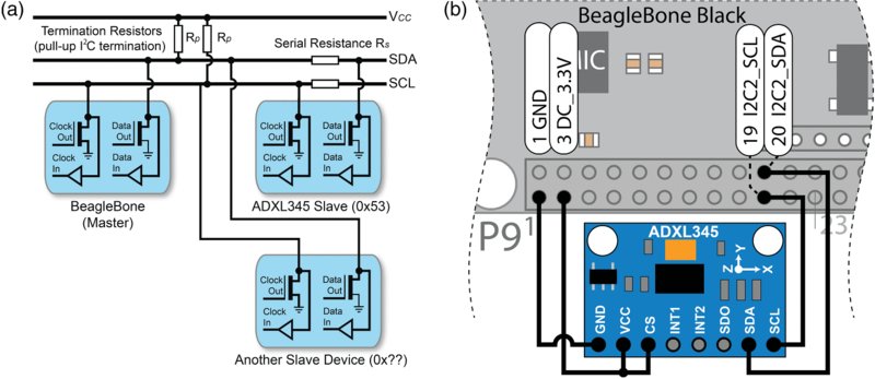
Figure 8-1 (a) The I2C bus configuration; (b) connecting the ADXL345 to the I2C2 bus on the BBB
Transmission line capacitance has a huge impact on data transmission rates. In Chapter 4 (see Figure 4‐10), when a 10 μF capacitor is connected in parallel with a resistive load and an AC voltage supply is applied, the capacitor had a very clear smoothing effect on the voltage across the load. This smoothing effect is unwelcome in the transmission of digital data—for example, if a random binary signal (0 V–3.3 V) switches at a high frequency, then severe smoothing could result in a constant 1.65 V signal, which carries no binary information at all. Typically, the longer the bus length and the more I2C devices that are attached to it, then the slower the speed of data transmission. There are I2C repeaters available that act as current amplifiers to help solve the problems associated with long lines.
The BBB supports bus frequencies of up to 400 kHz. NXP (formerly a division of Philips) has newer I2C Fast‐mode Plus (FM+) devices that can communicate at up to 1 MHz,1 but this capability is not available on the BBB.
The I2C bus requires pull‐up resistors (RP) on both the SDA and SCL lines, as illustrated in Figure 8-1(a). These are called termination resistors and they usually have a value of between 1 kΩ and 10 kΩ. Their role is to pull the SDA and SCL lines up to VCC when no I2C device is pulling them down to GND. This pull‐up configuration enables multiple master devices to take control of the bus, and for the slave device to “stretch” the clock signal (i.e., hold SCL low). Clock stretching can be used by the slave device to slow down data transfer until it has finished processing and is ready to transmit. These resistors are often already present on the breakout board that is associated with an I2C device. This can be a useful feature, but it may cause difficulty if you wish to use several breakout boards on the same bus.
The serial resistors (RS) shown in Figure 8-1(a) usually have low values (e.g., 250 Ω), and can help protect against overcurrent conditions. The I2C devices are attached to the SDA and SCL lines using Schmitt trigger inputs (see Chapter 4) to reduce the impact of signal noise by building in a degree of switching hysteresis.
In the I2C demonstration application discussed in this chapter, the BBB is the master device and the ADXL345 is the slave device. The ADXL345 is on a breakout board that already has 4.7 kΩ termination resistors on the board. The sensor is connected to the BBB as illustrated in Figure 8-1(b).
The I2C slave address is determined by the slave device itself. For example, the ADXL345 breakout board has the address 0x53, which is determined at manufacture. Many devices, including the ADXL345, have selection inputs that allow you to alter this value within a defined range. However, the breakout board to which the device is attached needs to support this change of address facility. In the following example, you could not connect two ADXL345 breakout board devices to the same bus, as their addresses would conflict. However, there are I2C multiplexers available that would enable you to overcome this problem.
Further documentation on the I2C bus is available from NXP directly at tiny.cc/ebb802.
The ADXL345 Accelerometer
The Analog Devices ADXL345 is a small, low‐cost accelerometer that can measure angular position with respect to the direction of Earth’s gravitational force. For example, a single‐axis accelerometer at rest on the surface of Earth, with the sensitive axis parallel to Earth’s gravity, will measure an acceleration of 1g (9.81 m/s2) straight upward. While accelerometers provide absolute orientation measurement, they suffer from high‐frequency noise, so they are often paired with gyroscopes for accurate measurement of change in orientation (e.g., in game controllers). However, accelerometers have excellent characteristics for applications in which low‐frequency absolute rotation is to be measured. For simplicity, an accelerometer is used on its own in the following discussions, because the main aim is to impart an understanding of the I2C bus.
The ADXL345 can be set to measure values with a fixed 10‐bit resolution, or using a 13‐bit resolution at up to ±16 g. It can be interfaced to the BBB using the I2C or SPI bus, which makes it an ideal sensor to use in this chapter as an example device. Even if you do not have this particular sensor, the following discussion is fully representative of the steps required to connect any type of I2C sensor to the BBB. The chapter web page identifies suppliers from whom you can purchase this particular sensor.
The data sheet for the ADXL345 is an important document that should be read along with this chapter. It is linked from the chapter web page or at www.analog.com/ADXL345 (or tiny.cc/ebb801).
The physical connection to the ADXL345 is illustrated in Figure 8-1(b). When the CS input is tied high, the ADXL345 is placed in I2C mode. The breakout board contains the resistors that are required for the I2C bus to work correctly. The ADXL345’s ALT Address pin is fixed to GND on the breakout board, placing the device at I2C address 0x53.
The I2C0 and I2C2 buses are present by default in the Debian BBB image and, perhaps erroneously, they map to the Linux device names i2c‐0 and i2c‐1, respectively. You can enable the second public I2C bus (see Table 8-1), i2c‐2 (I2C1) using the following command:
molloyd@beaglebone:/dev$ sudo sh ‐c "echo BB‐I2C1 > $SLOTS"
molloyd@beaglebone:/dev$ ls i2*
i2c-0  i2c-1  i2c-2
Table 8-1 I2C Buses on the BBB Debian Image
| H/W BUS | S/W DEVICE | SDA PIN | SCL PIN | DESCRIPTION |
| I2C0 | /dev/i2c‐0 |
N/A | N/A | Internal bus for HDMI control. |
| I2C1 | /dev/i2c‐2 |
P9_18 | P9_17 | General I2C bus. Disabled by default. |
| I2C2 | /dev/i2c‐1 |
P9_20 | P9_19 | General I2C bus. Enabled by default. |
Using Linux I2C‐Tools
Linux provides a set of tools, called i2c‐tools, for interfacing to I2C bus devices; it includes a bus probing tool, a chip dumper, and register‐level access helpers. These tools are already installed on the BBB Debian image, but they can be updated or installed on different images using the following:
molloyd@beaglebone:~$ sudo apt‐get install i2c‐tools
i2c-tools is already the newest version.
i2cdetect
The first step is to detect that the device is present on the bus. When the second public I2C bus is enabled, and the clock line (SCL) or data line (SDA) are not connected to any device, the i2cdetect command will display the following output:
molloyd@beaglebone:~$ i2cdetect ‐l
i2c-0  i2c     OMAP I2C adapter     I2C adapter
i2c-1  i2c     OMAP I2C adapter     I2C adapter
i2c-2  i2c     OMAP I2C adapter     I2C adapter
The /dev/i2c‐1 bus can then be probed for connected devices:
molloyd@beaglebone:~$ i2cdetect ‐y ‐r 1
      0  1  2  3  4  5  6  7  8  9  a  b  c  d  e  f
00:     -- -- -- -- -- -- -- -- -- -- -- -- -- -- --
10:  -- -- -- -- -- -- -- -- -- -- -- -- -- -- -- --
20:  -- -- -- -- -- -- -- -- -- -- -- -- -- -- -- --
30:  -- -- -- -- -- -- -- -- -- -- -- -- -- -- -- --
40:  -- -- -- -- -- -- -- -- -- -- -- -- -- -- -- --
50:  -- -- -- -- UU UU UU UU -- -- -- -- -- -- -- --
60:  -- -- -- -- -- -- -- -- -- -- -- -- -- -- -- --
70:  -- -- -- -- -- -- -- --
where the addresses 0x03 to 0x77 are displayed by default. Using ‐a will display the full range 0x00 to 0x7F. When -- is displayed, the address was probed but no device responded. When UU is displayed, probing was skipped, as the address is already in use by a driver. You can identify which driver by using the following (0x54 in this example):
molloyd@beaglebone:/sys/bus/i2c/devices/1‐0054$ cat modalias
i2c:24c256
When the ADXL sensor is physically connected to the I2C bus (I2C2) as shown in Figure 8-1(b), the I2C2 bus can be probed again using the same command:
molloyd@beaglebone:~$ i2cdetect ‐y ‐r 1
     0  1  2  3  4  5  6  7  8  9  a  b  c  d  e  f
...
50: -- -- -- 53 UU UU UU UU -- -- -- -- -- -- -- --
...
and if the device is functioning and correctly wired, it will appear at its pre‐defined address, which is 0x53 for this breakout board implementation.
Running i2cdetect on the internal I2C0 bus will highlight that there is already a device at 0x34, which relates to the consumer electronics control (CEC) interface on the HDMI framer for the BBB. Address 0x70 is also used by the HDMI framer.
molloyd@beaglebone:~$ i2cdetect ‐y ‐r 0
     0  1  2  3  4  5  6  7  8  9  a  b  c  d  e  f
...
30: -- -- -- -- 34 -- -- -- -- -- -- -- -- -- -- --
...
i2cdump
The i2cdump command can be used to read in the values of the registers of the device attached to an I2C bus and display them in a hexadecimal block form. You should not use this command without consulting the datasheet for the slave device, as in certain modes the i2cdump command will write to the device. The ADXL345 can be safely probed, and its output should be given by
molloyd@beaglebone:~$ i2cdump ‐y 1 0x53
No size specified (using byte-data access)
     0  1  2  3  4  5  6  7  8  9  a  b  c  d  e  f    0123456789abcdef
00: e5 00 00 00 00 00 00 00 00 00 00 00 00 00 00 4a    ?..............J
10: 00 00 10 00 00 00 00 00 00 00 00 00 00 00 00 00    ..?.............
20: 00 00 00 00 00 00 00 00 00 00 00 00 0a 00 00 00    ............?...
30: 02 00 00 00 00 00 00 00 00 00 00 00 00 00 00 00    ?...............
where many of the registers are empty because the device is in power‐saving mode by default. However, you can see that the first value at address 0x00 is 0xe5, and this value corresponds to the DEVID entry in Table 8-2—successful communication has been verified!
Table 8-2 Subset of the Registers in the ADXL345 Register Map
| ADDR | NAME | TYPE | DESCRIPTION |
| 0x00 | DEVID |
R | The device ID: This should be 111001012, which is E516. Most devices have a fixed ID at the address 0x00, which is a useful check on a successful connection. |
| 0x2D | POWER_CTL |
R/W | Power‐saving features control: Six bits that specify the sleep mode, measurement mode, etc. (see page 25 of the datasheet, register 0x2D). For example, 000010002 places the device in measurement mode with no sleep functionality enabled. |
| 0x31 | DATA_FORMAT |
R/W | Data format control: Seven bits that set the self‐test, SPI mode, interrupt inversion, zero bit, resolution, justify bit, and g range settings (two bits); e.g., 000001002 would set the range to ±2 g in 10‐bit mode, with left‐justified (MSB) mode (see page 26 of the datasheet, register 0x31). |
| 0x32 | DATAX0 |
R | X‐Axis Data 0: One byte containing the least significant byte of the X‐axis acceleration data. |
| 0x33 | DATAX1 |
R | X‐Axis Data 1: Most significant byte |
| 0x34 | DATAY0 |
R | Y‐Axis Data 0: Least significant byte |
| 0x35 | DATAY1 |
R | Y‐Axis Data 1: Most significant byte |
| 0x36 | DATAZ0 |
R | Z‐Axis Data 0: Least significant byte |
| 0x37 | DATAZ1 |
R | Z‐Axis Data 1: Most significant byte |
From Table 19 in the Analog Devices ADXL345 datasheet. There are 30 publicly accessible registers in total.
As previously stated, the datasheet for the ADXL345 from Analog Devices is available at www.analog.com/ADXL345. It is a comprehensive and well‐written datasheet that details every feature of the device. In fact, the real challenge in working with new bus devices is in decoding the datasheet and the intricacies of the device’s behavior. The ADXL345 has 30 public registers and Table 8-2 lists those that are accessed in this chapter. Other registers enable you to set power save inactivity periods, orientation offsets, and interrupt settings for free‐fall, tap, and double‐tap detection.
The x, y, and z‐axis acceleration values are stored using a 10‐bit or 13‐bit resolution; therefore, two bytes are required for each reading, as the data is in 16‐bit two’s complement form (see Chapter 4). To sample at 13 bits, the ADXL345 must be set to the ±16 g range. Figure 8-2 (from the ADXL345 datasheet) describes the signal sequences required to read and write to the device.
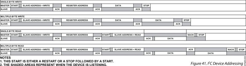
Figure 8-2 Timings required for single/multiple read/write operations on the ADXL345 device
Image courtesy of Analog Devices, Inc.
For example, to write a single byte to a device register, the master/slave access pattern in the first row is used as follows:
- The master sends a start bit (i.e. it pulls SDA low, while SCL is high).
- While the clock toggles, the seven‐bit slave address is transmitted one bit at a time.
- A read bit (1) or write bit (0) is sent, depending on whether the master wants to read or write to/from a slave register.
- The slave then responds with an acknowledge bit (ACK = 0).
- In write mode, the master sends a byte of data one bit at a time, after which the slave sends back an ACK bit. To write to a register, the register address is sent, followed by the data value to be written.
- Finally, to conclude communication, the master sends a stop bit (i.e., it allows SDA to float high, while SCL is high).
These handshaking sequences will shortly be confirmed by reading and writing from/to the device and by physically analyzing the I2C bus communication.
i2cget
The i2cget command can be used to read the value of a register in order to test the device, or as an input for Linux shell scripts. For example, to read the DEVID of the attached device, which should be 0xE5 in this case, use the following:
molloyd@beaglebone:~$ i2cget ‐y 1 0x53 0x00
0xe5
The Analog Discovery digital logic analyzer functionality can be used to physically analyze the I2C bus in order to view the interaction of SDA and SCL signals as data is written to and read from the I2C bus. The logic analyzer functionality has interpreters for I2C buses, SPI buses, and UART devices, which can display the hexadecimal equivalents of the serial data carried on the bus. Figure 8-3 captures the signal transitions of the i2cget command used in the preceding example. Here, you can see that the clock is running at I2C standard data transfer mode (100 kHz). This accelerometer also supports fast data transfer mode (400 kHz). The timing signals displayed in Figure 8-3 confirm those on the third row of Figure 8-2 for a single byte read. The top row in Figure 8-3 (I2C2) details the interpretation of the SDA and SCL signals that are displayed on the second and third rows.
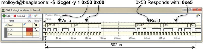
Figure 8-3 Using i2cget to read the DEVID register value
i2cset
The i2cset command can be used to set a register. This is required, for example, to take the ADXL345 out of power‐saving mode, by writing 0x08 to the POWER_CTL register, which is at 0x2D. The value is written and then confirmed as follows:
molloyd@beaglebone:~$ i2cset ‐y 1 0x53 0x2D 0x08
molloyd@beaglebone:~$ i2cget ‐y 1 0x53 0x2D
0x08
If the i2cdump command is then used, the registers 0x32 through 0x37 (as identified in Table 8-2) will display the acceleration values, which change as the sensor is physically rotated and the i2cdump command is repeatedly called:
molloyd@beaglebone:~$ i2cdump ‐y 1 0x53
No size specified (using byte-data access)
     0  1  2  3  4  5  6  7  8  9  a  b  c  d  e  f    0123456789abcdef
00: e5 00 00 00 00 00 00 00 00 00 00 00 00 00 00 4a    ?..............J
10: 82 00 30 00 00 01 fc 1d 00 00 00 22 00 00 00 00    ?.0..???..."....
20: 00 00 00 00 00 00 00 00 00 00 00 00 0a 08 00 00    ............??..
30: 83 01 06 00 f1 ff 75 00 00 00 00 00 00 00 00 00    ???.?.u.........
The next step is to write program code that can interpret the values contained in these registers. First, C code to do this is presented, and then a C++ class is written that introduces a more structured programming approach.
I2C Communication in C
The ADXL345 digital accelerometer measures acceleration in three axes using analog sensors, which are internally sampled and filtered according to the settings that are placed in its registers. The acceleration values are then available for you to read from these registers. Therefore, the sensor performs timing‐critical signal processing that would otherwise have to be performed by the BBB. However, further numerical processing is still required in converting the 16‐bit two’s complement values stored in its registers into values that describe angular pitch and roll. As such, C/C++ is a good choice for this type of numerical processing.
The first C programming example, in Listing 8‐1, simply reads in all of the registers and displays the first register (0x00). This can be used to display the device ID (DEVID), and thereby confirm that the C program is working correctly. Many other I2C devices have device IDs at the address 0x00, which do not change as the device is manipulated. Therefore, this is a useful first test.
The code can then be executed as follows:
molloyd@beaglebone:~/exploringbb/chp08/test/i2c$ ./build
Building the ADXL345 example applications
molloyd@beaglebone:~/exploringbb/chp08/test/i2c$ ./testADXL345
Starting the ADXL345 test application
The Device ID is: 0xe5
This program outputs that the device ID value is 0xE5, which confirms that the ADXL345 is attached at the address 0x53 and therefore that the code is working correctly.
To display all the registers and to process the accelerometer values, a new program (chp08/i2c/test/ADXL345.cpp) is written that breaks the calls into functions, such as the readRegisters() function:
// Read the entire 40 registers into the buffer (10 reserved)
int readRegisters(int file){
   // Writing a 0x00 to the device sets the address back to
   //  0x00 for the coming block read
   writeRegister(file, 0x00, 0x00);
   if(read(file, dataBuffer, BUFFER_SIZE)!=BUFFER_SIZE){
      cout << "Failed to read in the full buffer." << endl;
      return 1;
   }
   if(dataBuffer[DEVID]!=0xE5){
      cout << "Problem detected! Device ID is wrong" << endl;
      return 1;
   }
   return 0;
}
This code writes the address 0x00 to the device, causing it to send back the full 0x40 registers (BUFFER_SIZE). In order to process the two raw 8‐bit acceleration registers, code to combine two bytes into a single 16‐bit value is written as follows:
// short is 16-bits on the BBB
short combineValues(unsigned char upper, unsigned char lower){
   //shift the most significant byte left by 8 bits and OR with the
   // least significant byte
   return ((short)upper<<8)|(short)lower;
}
The types of the data are vital in this function, as the register data is returned in two’s complement form. If an int type (of size 32‐bits, int32_t) were used instead of short 16‐bit integral data (int16_t), then the sign bit would be dislocated. This function shifts the upper byte left (multiply) by eight places (equivalent to a multiplication by 28 = 256) and ORs the result with the lower byte, which replaces the lower byte with eight zeroes that are introduced by the shift). This results in a 16‐bit signed value (int16_t) that has been created from two separate 8‐bit values (uint8_t). When executed, the ADXL345.cpp application will give the following output, with the program updating the acceleration data on the same console line:
molloyd@beaglebone:~/exploringbb/chp08/i2c/test$ ./ADXL345
Starting the ADXL345 sensor application
The Device ID is: e5
The POWER_CTL mode is: 08
The DATA_FORMAT is: 00
X=13 Y=-35 Z=232 sample=17
Additional code is required to convert these values into a pitch and roll form. This is added to the C++ class in the next section. For your information, the logic analyzer indicates that it takes 4.19 ms to read in the full set of 40 registers at a bus speed of 100 kHz.
Wrapping I2C Devices with C++ Classes
Object‐oriented programming is described in Chapter 5 as a suitable framework for developing code for embedded systems. As a programmer, one of your key aims should be to avoid writing the same code twice. You could repeatedly copy‐and‐paste code from project to project, but if you subsequently discover an error, it will have to be corrected in several locations. A danger arises when you forget to change the copied code in one or more locations.
A specific C++ class can be written to wrap the functionality of the ADXL345 accelerometer; because it is likely that you will need to write code to control several different types of I2C device, it would be useful if the general I2C code could be extracted and placed in a parent class. To this end, a class has been written for this chapter called I2CDevice that captures the general functionality you would associate with an I2C bus device. You can extend this code to control any type of I2C device. It can be found in the I2CDevice.cpp andI2CDevice.h files in the chp08/i2c/cpp/ directory. Later in this chapter the code is further restructured and placed in the /library/bus GitHub directory. The class has the structure as described in Listing 8‐2.
The implementation code is available in the chp08/i2c/cpp/ directory. This class can be extended to control any type of I2C device, and in this case it is used as the parent of a specific device implementation class called ADXL345. Therefore, you can say that ADXL345 IS‐A I2CDevice. This inheritance relationship means that any methods available in the I2CDevice class are now available in the ADXL345 class in Listing 8‐3 (e.g., readRegister()).
The enumeration structures are used to constrain the range and resolution selections to contain only valid options. A short example (application.cpp) can be used to test this structure, as follows:
int main(){
   ADXL345 sensor(1,0x53);   // sensor is on bus 1 at the address 0x53
   sensor.setResolution(ADXL345::NORMAL);   // using 10-bit resolution
   sensor.setRange(ADXL345::PLUSMINUS_4_G); // range is +/-4g
   sensor.displayPitchAndRoll();   // put the sensor in display mode
   return 0;
}
This code can be built and executed as follows, where the pitch and roll are angular values that each vary between ±90°:
/chp08/i2c/cpp$ g++ application.cpp I2CDevice.cpp ADXL345.cpp ‐o ADXL345
/chp08/i2c/cpp$ ./ADXL345
Pitch:5.71592 Roll:-31.5256
You can use this general structure to build wrapper classes for any type of I2C sensor, and it will work perfectly well. However, later in this chapter an additional software design issue must be addressed, meaning that the structure presented here for the ADXL345 class requires further modification.
SPI
The Serial Peripheral Interface (SPI) bus is a fast, full‐duplex synchronous serial data link that enables devices such as the BBB to communicate with other devices over short distances. Therefore, like I2C, the SPI bus is synchronous, but unlike the I2C bus the SPI bus is full‐duplex. This means that it can transmit and receive data at the same time, by using separate lines for both sending data and receiving data.
In this section the SPI bus is introduced, and two separate applications are developed. The first uses the SPI bus to drive an LED bar graph display using the ubiquitous 74HC595 eight‐bit shift register. The second application interfaces to the ADXL345 accelerometer again, this time using its SPI bus instead of the I2C bus used previously.
SPI Hardware
SPI communication takes place between a single master device and one or more slave devices. Figure 8-4(a) illustrates a single slave example, where four signal lines are connected between the master and slave devices. To communicate with the slave device, the following steps take place:
- The SPI master defines the clock frequency at which to synchronize the data communication channels.
- The SPI master pulls the chip select (CS) line low, which activates the client device—it is therefore said to be active low. This line is also known as slave select (SS).
- After a short delay, the SPI master issues clock cycles, sending data out on the master out-slave in (MOSI) line and receiving data on the master in-slave out (MISO) line. The SPI slave device reads data from the MOSI line and transmits data on the MISO line. One bit is sent and one bit is received on each clock cycle. The data is usually sent in one‐byte (eight‐bit) chunks.
- When complete, the SPI master stops sending a clock signal and then pulls the CS line high, deactivating the SPI slave device.
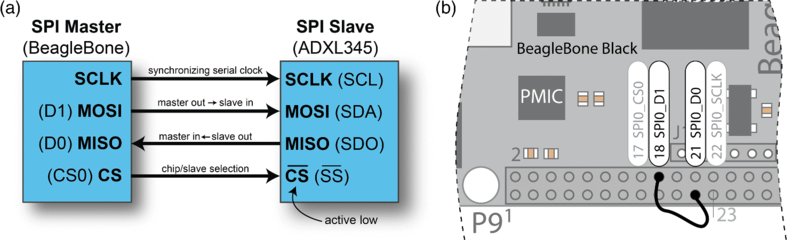
Figure 8-4 (a) Using SPI to connect to one slave; (b) testing SPI using a Linux configuration
Unlike I2C, the SPI bus does not require pull‐up resistors on the communication lines, so connections are very straightforward. A summary comparison of I2C versus SPI is provided in Table 8-3.
Table 8-3 Comparison of I2C versus SPI on the BBB
| I2C | SPI | |
| Connectivity | Two wires, to which up to 128 addressable devices can be attached. | Typically four wires, and requires additional logic for more than one slave device. |
| Data rate | I2C fast mode is 400 kHz. Uses half‐duplex communication. | Faster performance, typically over 10 MHz. Full duplex (except three‐wire variant). |
| Hardware | Pull‐up resistors required. | No pull‐up resistors required. |
| BBB support | Fully supported with two external buses (plus one internal). | Fully supported with two buses. Only one slave selection pin on each bus. |
| Features | Can have multiple masters. Slaves have addresses, acknowledge transfer, and can control the flow of data. | Simple and fast, but only one master device, no addressing, and no slave control of data flow. |
| Application | Intermittently accessed devices, e.g., real‐time clock, EEPROMs. | For devices that provide data streams, e.g., ADCs. |
The SPI bus operates using one of four different modes, which is chosen according to the specification defined in the SPI slave device’s datasheet. Data is synchronized using the clock signal, and one of the SPI communication modes described in Table 8-4 is set to describe how the synchronization is performed. The clock polarity defines whether the clock is low or high when it is idle (i.e., when CS is high). The clock phase defines whether the data on the MOSI and MISO lines is captured on the rising edge or falling edge of the clock signal. When a clock’s polarity is 1, the clock signal is equivalent to an inverted version of the same signal with a polarity of 0. Therefore, a rising edge on one form of clock signal polarity is the equivalent of a falling edge on the other. You need to examine the datasheet for the slave device in order to determine the SPI mode.
Table 8-4 SPI Communication Modes
| MODE | CLOCK POLARITY (CPOL) | CLOCK PHASE (CPHA) |
| 0 | 0 (low at idle) | 0 (data captured on the rising edge of the clock signal) |
| 1 | 0 (low at idle) | 1 (data captured on the falling edge of the clock signal) |
| 2 | 1 (high at idle) | 0 (data captured on the falling edge of the clock signal) |
| 3 | 1 (high at idle) | 1 (data captured on the rising edge of the clock signal) |
The SPI protocol does not define a maximum data rate, flow control, or communication acknowledgment. Therefore, implementations vary from device to device, so it is very important to study the datasheet of each type of SPI slave device. There are some three‐wire SPI variants that use a single bidirectional MISO/MOSI line instead of two individual lines. For example, the ADXL345 sensor supports I2C, and both four‐wire and three‐wire SPI communication.
SPI on the BBB
The P9 header layout in Figure 6‐7 of Chapter 6 identifies that the SPI0 and SPI1 buses are accessible from this header. SPI1 clashes with the mcasp0_pins, so to use SPI1 you have to disable HDMI. As illustrated in Figure 8-4(b), the pins for SPI0 are as follows:
- Chip Select: P9_17 spi0_cs0 (Mode 0) $PINS 87 Offset 0x15C.
- MOSI: P9_18 spi0_d1 (Mode 0) $PINS 86 Offset 0x158.
- MISO: P9_21 spi0_d0 (Mode 0) $PINS 85 Offset 0x154.
- Clock: P9_22 spi0_sclk (Mode 0) $PINS 84 Offset 0x150.
The SPI0 and SPI1 buses are disabled by default, so to enable them you use device tree overlays, as described in Chapter 6. The BB‐SPIDEV0‐00A0.dts file defines how this overlay is configured, with internal pull‐up resistors enabled and inputs/outputs defined as shown in the partial listing in Listing 8‐4. The full listing is linked from the web page associated with this chapter.
Enabling the First SPI Bus (SPI0)
To enable the SPI buses, the requisite overlay must be loaded, using the same syntax discussed in Chapter 6:
molloyd@beaglebone:/lib/firmware$ ls *SPI*
ADAFRUIT‐SPI0‐00A0.dtbo  BB‐SPIDEV0‐00A0.dtbo  BB‐SPIDEV1A1‐00A0.dtbo
ADAFRUIT-SPI1-00A0.dtbo  BB-SPIDEV1-00A0.dtbo
molloyd@beaglebone:/lib/firmware$ sudo sh ‐c "echo BB‐SPIDEV0 > $SLOTS"
molloyd@beaglebone:/lib/firmware$ cat $SLOTS
...
 4: ff:P-O-L Bone-LT-eMMC-2G,00A0,Texas Instrument,BB-BONE-EMMC-2G
 5: ff:P-O-L Bone-Black-HDMI,00A0,Texas Instrument,BB-BONELT-HDMI
 7: ff:P‐O‐L Override Board Name,00A0,Override Manuf,BB‐SPIDEV0
If the overlay is loaded correctly into a slot, then there will now be two new devices in /dev as follows, where spidev1.0 means chip select 0 on bus 1:
molloyd@beaglebone:/lib/firmware$ cd /dev
molloyd@beaglebone:/dev$ ls sp*
spidev1.0  spidev1.1
Testing the SPI Bus
To test the SPI bus you can use a program called spidev_test.c that is available from www.kernel.org. However, the latest version at the time of writing has added support for dual and quad data‐wire SPI transfers, which are not supported on the BBB. An older version of this code has been placed in /chp08/spi/spidev_test/ and can be built using the following:
~/exploringbb/chp08/spi/spidev_test$ gcc spidev_test.c ‐o spidev_testBecause the pins have been enabled in pull‐up mode, the output displayed by the spidev_test program should be 0xFF when nothing is connected to the bus and the test program is executed:
~/exploringbb/chp08/spi/spidev_test$ ./spidev_test
spi mode: 0
bits per word: 8
max speed: 500000 Hz (500 KHz)
FF FF FF FF FF FF
FF FF FF FF FF FF
FF FF FF FF FF FF
FF FF FF FF FF FF
FF FF FF FF FF FF
FF FF FF FF FF FF
FF FF
Connect the spi0_d1 (P9_18) and spi0_d0 (P9_21) header input/outputs together so that the BBB MOSI is connected to the BBB MISO, as in Figure 8-4(b). When the test program is executed again, the output should be as follows:
~/exploringbb/chp08/spi/spidev_test$ ./spidev_test
spi mode: 0
bits per word: 8
max speed: 500000 Hz (500 KHz)
FF FF FF FF FF FF
40 00 00 00 00 95
FF FF FF FF FF FF
FF FF FF FF FF FF
FF FF FF FF FF FF
DE AD BE EF BA AD
F0 0D
This is the exact block of data that is defined in the tx[] array inside the spidev_test.c code. Therefore, in this case, the block of data has been successfully transmitted from P9_18 (MOSI) and received by P9_21 (MISO). This program can be executed on the second SPI bus as follows:
~/exploringbb/chp08/spi/spidev_test$ ./spidev_test ‐D /dev/spidev2.0A First SPI Application (74HC595)
The first application to test the SPI bus is illustrated in Figure 8-5. It uses a 74HC595, which is an eight‐bit shift register with latched outputs that can be supplied at 3.3 V logic levels. The 74HC595 can typically be used at frequencies of 20 MHz or greater, depending on the supply voltage VCC. The circuit in Figure 8-5 uses an LED bar graph and a resistor network in order to minimize the number of connections, but an equivalent circuit with individual LEDs and resistors is just as functionally valid.
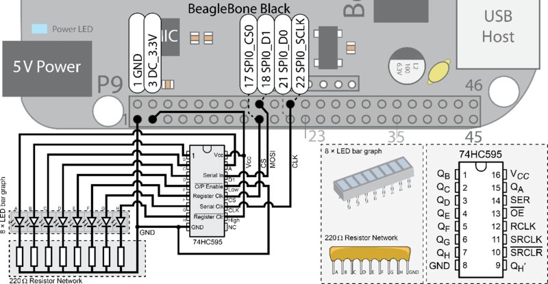
Figure 8-5 The 74HC595 SPI example
Wiring the 74HC595 Circuit
The 74HC595 is connected to the BBB using three of the four SPI lines, as a MISO response from the 74HC595 is not required (you could connect the MISO line to QH’ as a further test). The connections are as follows:
- P9_22 SPI0_SCLK is connected to the Serial Clock input (pin 11) of the 74HC595. This line is used to synchronize the transfer of SPI data on the MOSI line.
- P9_18 SPI0_D1 is the MOSI line and is used to transfer the data from the BBB to the 74HC595 Serial Input (pin 14). This will send one byte (eight bits) at a time, which is the full capacity of the 74HC595.
P9_17 SPI0_CS0 is the slave select line. This line is important, as it is used to latch the data to the output of the 74HC595 when its state transitions from low to high. As such, it is connected to the Register Clock input (pin 12) of the 74HC595. The LEDs on the bar graph will light according to the bytes that are transferred. For example, sending 0xAA should light every second LED on the bar graph if the setup is working correctly, as 0xAA = 101010102. This circuit is useful for controlling eight outputs using a single serial data line and it can be extended further by daisy chaining 74HC595 ICs together. This is particularly useful for driving arrays of seven‐segment displays, and is discussed in the next chapter.
Once the overlay is loaded, you can write directly to the device as follows to light most of the LEDs (‐n suppresses the newline character, ‐e enables escape character interpretation, and x escapes the subsequent value as hexadecimal):
molloyd@beaglebone:/dev$ echo ‐ne "xFF" > /dev/spidev1.0The following will turn most of the LEDs off:
molloyd@beaglebone:/dev$ echo ‐ne "x00" > /dev/spidev1.0However, this may not work exactly as expected, as the current SPI communication mode does not align by default with the operation of the 74HC595, as wired in Figure 8-5. As a test, it is useful to confirm that there is some level of response from the circuit. The transfer mode issue is corrected within the following code example.
SPI Communication Using C
A C program can be written to control the LED bar graph. Basic open() and close() operations on the /dev/spidevX.Y devices work, but if you need to alter the low‐level SPI transfer parameters, then a more sophisticated interface is required.
The following program uses the Linux user space SPI API, which supports reading and writing to SPI slave devices. It is accessed using Linux ioctl() requests, which support SPI through the sys/ioctl.h and linux/spi/spidev.h header files. A full guide on the use of this API is available at www.kernel.org/doc/Documentation/spi/.
The program in Listing 8‐5 will cycle the LEDs in the bar graph from 00000000 to 11111111 and output the count to a Linux terminal. Thetransfer() function is the most important part of the code example.
The main() function sets the SPI control parameters. These are ioctl() requests that allow you to override the device’s current settings for parameters such as the following, where xx is both RD (read) and RW (write):
SPI_IOC_xx_MODE: The SPI transfer mode (0–3)SPI_IOC_xx_BITS_PER_WORD: Number of bits in each wordSPI_IOC_xx_LSB_FIRST: 0 is MSB first, 1 is LSB firstSPI_IOC_xx_MAX_SPEED_HZ: Maximum transfer rate in Hz
The current Linux implementation provides for synchronous transfers only. When executed, this code will result in the following output, where the count value continually increases on the one line of the terminal window:
molloyd@beaglebone:~/exploringbb/chp08/spi/spi595Example$ ./spi595
SPI Mode is: 3
SPI Bits is: 8
SPI Speed is: 1000000
Counting through all of the LEDs:
 163
At the same time, this code is sending signals to the 74HC595 as captured using the SPI interpreter of the Analog Discovery in Figure 8-6, when the count is at 16310 = 0xA3. At this point in time, the CS line is pulled low, while a clock (SCLK) that is “high at idle” is toggled by the SPI master after a short delay. The data is then sent on the SDIO line, MSB first, to the 74HC595, and it is transferred on the rising edge of the clock signal. This confirms that the SPI transfer is taking place in mode 3, as described in Table 8-4.
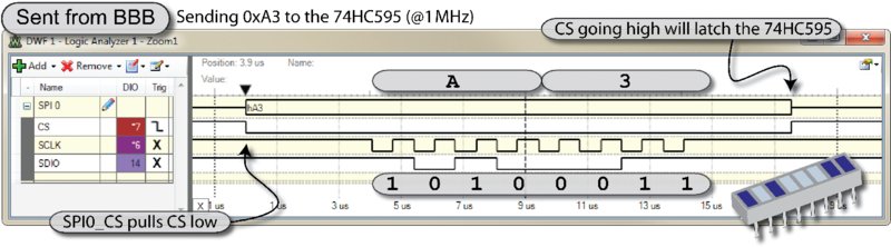
Figure 8-6 The 74HC595 SPI signal and output
The total transfer takes less than 18 μs. If the channel were held open, it would be capable of transferring a maximum of 91 kB/s (727 kb/s) at 1 MHz, if there were no delay between each byte transfer.
Bidirectional SPI Communication in C++
The 74HC595 example sent data from the BBB to the 74HC595, and as such is a unidirectional communication example. It is possible to use the QH, serial output (pin 9) of the 74HC595 as a test example of bidirectional data transfer, because when eight bits of data are shifted into the 74HC595, the previous eight bits are shifted out through this output pin. The pin could then be connected to the MISO input on the BBB. However, a more generally applicable example of bidirectional communication that involves register addressing can be demonstrated with the ADXL345 sensor.
As discussed previously, the AXL345 has both an I2C and an SPI communications interface. This makes it a useful device with which to examine bidirectional SPI communication here, as the register structure has already been discussed in detail. In addition, its use brings up some interesting software design challenges. The second SPI bus is used in the following example, so that it can be tested and so that the previous circuit can be temporarily preserved.
The Second SPI Bus (SPI1)
The second SPI Bus, SPI1, can be enabled, but not if the HDMI interface is in use. The HDMI overlay can be disabled using the steps described in Chapter 6 (see “Removing an Overlay”). When the second overlay is loaded, the slots should be populated as follows:
molloyd@beaglebone:~$ sudo sh ‐c "echo BB‐SPIDEV1 > $SLOTS"
molloyd@beaglebone:~$ cat $SLOTS
...
 4: ff:P-O-L Bone-LT-eMMC-2G,00A0,Texas Instrument,BB-BONE-EMMC-2G
 5: ff:P-O-– Bone-Black-HDMI,00A0,Texas Instrument,BB-BONELT-HDMI
 6: ff:P-O-– Bone-Black-HDMIN,00A0,Texas Instrument,BB-BONELT-HDMIN
 7: ff:P-O-L Override Board Name,00A0,Override Manuf,BB-SPIDEV1
Once loaded, the SPI bus has the following configuration:
- Chip Select: P9_28 spi1_cs0 (Mode 3) $PINS 103 Offset 0x19C
- MOSI: P9_30 spi1_d1 (Mode 3) $PINS 102 Offset 0x198
- MISO: P9_29 spi1_d0 (Mode 3) $PINS 101 Offset 0x194
- Clock: P9_31 spi1_sclk (Mode 3) $PINS 100 Offset 0x190
Depending on the number of SPI overlays that you have loaded, the SPI1 device will appear as either spidev1.0 and spidev1.1 or spidev2.0 and spidev2.1. With both SPI buses enabled, you should see the following:
molloyd@beaglebone:/dev$ ls spi*
spidev1.0  spidev1.1  spidev2.0  spidev2.1
The ADXL345 SPI Interface
SPI is not a formal standard with a standards body controlling its implementation, and therefore it is vital that you study the datasheet for the device that you wish to attach to the BBB. In particular, the SPI communication timing diagram should be studied in detail. This is presented for the ADXL345 in Figure 8-7.
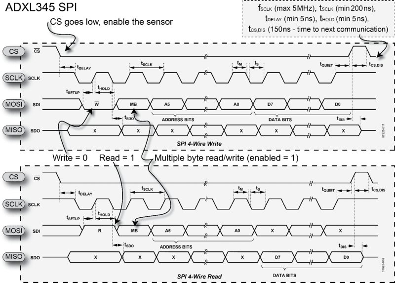
Figure 8-7 The ADXL345 SPI communication timing chart (from the ADXL345 datasheet)
Underlying image is courtesy of Analog Devices, Inc.
Note the following very important points, which can be observed directly from the datasheet:
- To write to an address, the first bit on the SDI line must be low. To read from an address the first bit on the SDI line must be high.
- The second bit is called MB. From further analysis of the datasheet, this bit enables multiple byte reading/writing of the registers (i.e., send the first address and data will be continuously read from that register forward). This leaves six bits in the first byte for the address (26 = 6410 = 4016), which is sufficient to cover the available registers.
- As shown in the figure, the SCLK line is high at rest and data is transferred on the rising edge of the clock signal. Therefore, the ADXL345 device must be used in communications mode 3 (refer to Table 8-4).
- When writing (top figure), the address (with a leading 0) is written to SDI, followed by the byte value to be written to the address.
- When reading (bottom figure), the address (with a leading 1) is written to SDI. A second byte is written to SDI and will be ignored. While the second (ignored) byte is being written to SDI, the response will be returned on SDO detailing the value stored at the register address.
Connecting the ADXL345 to the BBB
The ADXL345 breakout board can be connected to the SPI1 bus as illustrated in Figure 8-8, where MOSI on the BBB is connected to SDI and MISO is connected to SDO. The clock lines and the slave select lines are also interconnected.
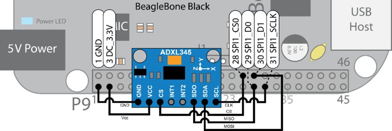
Figure 8-8 SPI1 Connection to the ADXL345
Wrapping SPI Devices with C++ Classes
A C++ class has also been written in order to wrap the software interface to the SPI bus, using the OOP techniques that are described in Chapter 5. Before discussing it, there is an interesting OOP design problem that needs to be solved. In theory, if your OOP structure is designed properly then you should never need to write the same code twice. This is desirable because copying and pasting code will result in twice the amount of code, which will need to be debugged and maintained. Earlier in this chapter a structure is presented whereby the class ADXL345 is a child of the I2CDevice class. That is a reasonable design given the information available at that point. However, because the ADXL345 also has an SPI interface, it is necessary now to update the software structure. One possible solution is illustrated in Figure 8-9(a), which is presented in a pseudo‐UML form.
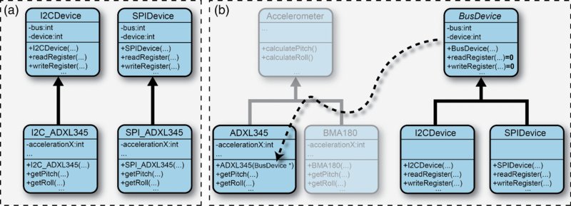
Figure 8-9 (a) Simple OOP structure (not recommended); (b) more appropriate OOP design
Unfortunately, this structure involves copying and pasting code, as the same code will have to be written in both the I2C_ADXL345 and the SPI_ADXL345 classes. As this code is implemented in C++, you could use some form of multiple inheritance, but you would have to build in function pointer switches, or explicitly indicate whether you are using the I2CDevice::readRegister() method or the SPIDevice::readRegister() method.
A different structure is presented in Figure 8-9(b). In this design, a new abstract class called BusDevice is created that describes, but does not implement, the methods that are common to both I2C and SPI devices (e.g., readRegister() or writeRegister()). The actual implementation of these methods is provided in the I2CDevice and SPIDevice child classes, respectively. The constructor of the ADXL345 class now expects an object of BusDevice. However, because it is an abstract class, you actually pass a pointer to an object of one of its child classes (I2CDevice or SPIDevice). The ADXL345 class code now only needs to be written in one location.
One additional advantage of this structure is that if you were writing code for different accelerometer types (e.g., the Bosch BMA180), then you could create a new general class (e.g., Accelerometer) that would contain functionality that is common to all accelerometer types, such as the numerical calculation of pitch and roll values.
This approach may seem overly complex, but the actual usage is very straightforward. For example, if you assume that two ADXL345 sensors are attached to the BBB, one to the SPI bus and the second to the I2C bus, you can use the exact same ADXL345 class to create two objects in the following way:
int main() {
   SPIDevice spi(1,0);
   ADXL345 acc1(&spi);
   acc1.displayPitchAndRoll(100);

   I2CDevice i2c(1,0x53);
   ADXL345 acc2(&i2c);
   acc2.displayPitchAndRoll(100);
}
The classes for controlling I2C and SPI devices have been added to the library directory of the GitHub repository in the /library/bus/ directory, and partial listings are provided in Listings 8‐6, 8‐7, and 8‐8.
The SPI class in Listing 8‐7 can also be used in a standalone form. For example, to read and write from the ADXL345 device without using a specific accelerometer child class, the following code structure can be used:
int main() {
   SPIDevice spi(1,0);             // chip select 0 on bus 1
   spi.setSpeed(1000000);          // set the speed to 1 MHz
   cout << "The device ID is: " << (int) spi.readRegister(0x00) << endl;
   spi.setMode(SPIDevice::MODE3);  // set the mode to Mode3
   spi.writeRegister(0x2D, 0x08);  // POWER_CTL for the ADXL345
   spi.debugDumpRegisters(0x40);   // Dump the 64 registers from 0x00
}
This will give the following output when built and executed (0xE5 = 22910):
molloyd@beaglebone:~$ ./SPITest
The device ID is: 229
SPI Mode: 3
Bits per word: 8
Max speed: 1000000
Dumping Registers for Debug Purposes:
e5 00 00 00 00 00 00 00 00 00 00 00 00 00 00 4a
82 00 30 00 00 01 ff 3a 00 00 00 6c 00 00 00 00
00 00 00 00 00 00 00 00 00 00 00 00 0a 08 00 00
02 00 05 00 fd ff e9 00 00 00 00 00 00 00 00 00
Once again, a logic analyzer is very useful for debugging problems that can occur with SPI bus communication. For example, Figure 8-10 captures a read operation at address 0x00. You may notice that the value that was sent was 0x80 and not 0x00. This is because (as detailed in Figure 8-7), the leading bit must be a 1 to read and a 0 to write from/to an address. Sending 0x00 is a write request to address 0x00 (which is not possible), and sending 0x80 (i.e., 10000000 + 00000000) is a request to read the value at address 0x00. The second bit is 0 in both cases, thus disabling multiple‐byte read functionality.
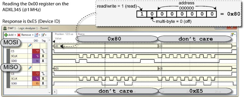
Figure 8-10 Reading the 0x00 register on the ADXL345 using SPI
Three‐Wire SPI Communication
The ADXL345 supports three‐wire SPI (half duplex). In this mode the data is read and transmitted on the same SDIO line. To enable this mode on the ADXL345, the value 0x40 must be written to the 0x31 (DATA_FORMAT) register and a 10 kΩ resistor should be placed between SD0 and VCC on the ADXL345. Figure 8-11 illustrates the communication that should take place.
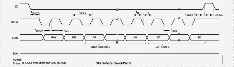
Figure 8-11 ADXL345 three‐wire SPI communication
Image courtesy of Analog Devices, Inc.
There is a draft project in place in the chp08/spi/spiADXL345/3‐wire directory that contains a device tree overlay, which sets the spi‐3wire property on the SPI bus fragment. Unfortunately, at the time of writing, there is no support for this mode in the current BBB Linux distribution.
Multiple SPI Slave Devices on the BBB
One of the advantages of the SPI bus is that it can be shared with multiple slave devices, provided that only one slave device is active when communication takes place. On most microcontrollers, GPIO pins can be used as slave selection pins, and a similar structure can be developed for the BBB. If you wish to allow the Linux SPI interface library code to retain control of the slave selection functionality, then a wiring configuration like that in Figure 8-12 could be used. This configuration uses OR gates and an inverter to ensure that only one CS input is pulled low at a single time. In Figure 8-12(a), the ADXL345 slave device is active when CS = 0 and GPIO = 0, and in Figure 8-12(b), the second slave device is active when CS = 0 and GPIO = 1.
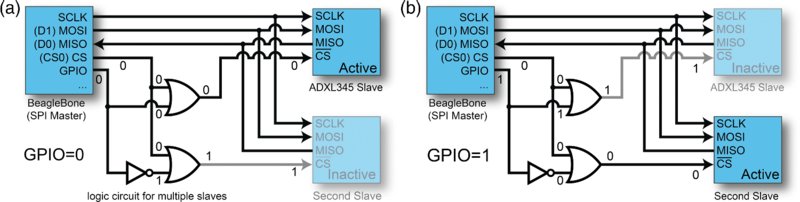
Figure 8-12 BBB control of more than one slave device using GPIO pins and additional logic
Depending on the particular slave devices being used, the GPIO output combined with a single inverter may be sufficient, as you could “permanently” pull the ![]() line low on the slave device, ignoring the CS output of the master. However, this would not work for the 74HC595 example, as the BBB’s CS line is used to latch the data to the output LEDs.
line low on the slave device, ignoring the CS output of the master. However, this would not work for the 74HC595 example, as the BBB’s CS line is used to latch the data to the output LEDs.
For more than two slave devices, a 3‐to‐8 line decoder, such as the 74HC138, would be a good solution. It has inverted outputs, which means that only one of its eight outputs is low at a single point in time. This device could be controlled using three of the BBB’s GPIOs and it could enable one of eight slave devices (23 = 8). There are also 4‐to‐16 line decoders with inverting outputs, such as the 74HC4515, which would enable you to control 16 slave devices with only four GPIOs (24 = 16). For both of these devices, the BBB CS output could be connected to their enable input(s).
UART
A universal asynchronous receiver/transmitter (UART) is a microprocessor peripheral device used for the serial transfer of data, one bit at a time, between two electronic devices. UARTs were originally standalone ICs, but now are often integrated with the host microprocessor/microcontroller. A UART is not, strictly speaking, a bus, but its capacity to implement serial data communications overlaps with similar capacities of the I2C and SPI buses described earlier. A UART is described as asynchronous because the sender does not have to send a clock signal to the recipient in order to synchronize the transmission, rather a communication structure is agreed upon that uses start and stop bits to synchronize the transmission of data. Because no clock is required, the data is typically sent using only two signal lines. Just like a regular telephone line, the transmit data connection (TXD) from one end is connected to the receive data connection (RXD) on the other end of the connection, and vice versa.
Traditionally, UARTs have been used with level converters/line drivers to implement interfaces such as RS‐232 or RS‐485, but for short‐distance communications, it is possible to use the original logic level for the UART outputs and inputs to enable two UARTs to communicate with each other. Note that this is a perfectly possible but nonstandardized use of UARTS.
The number of symbols per second is known as the baud rate or modulation rate. With certain encoding schemes a symbol could be used to represent two bits (i.e., four states, for example, by using quadrature phase‐shift keying (QPSK)). Then the bit rate would be twice the baud rate. However, for a simple bi‐level UART connection, the baud rate is the same as the bit rate.
The transmitter and receiver agree upon a bit rate before communication begins. The byte rate is somewhat lower than 1/8 of the bit rate, as there are overhead bits associated with the serial transmission of data. Transmission begins when the transmitter sends a start bit (logic low), as shown in Figure 8-13. On the receiver’s end, the falling edge of the start bit is detected and then after 1.5 bit periods, the first bit value is sampled. Every subsequent bit is sampled after 1.0 bit periods, until the agreed upon number of bits is transferred (typically seven or eight). The parity bit is optional (though both devices must be configured to either use it or not); if used, it can identify whether a transmission error has occurred. It would be high or low, depending on whether odd or even parity checking is employed. Finally, one stop bit is sent (or optionally two stop bits), which is always a logic high value. The examples that follow in this section all use a standard 8N1 form, which means that eight bits are sent in each frame, with no parity bits and one stop bit.
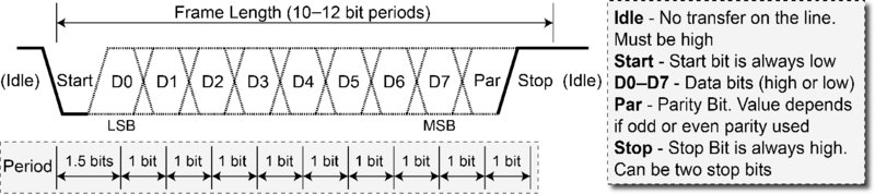
Figure 8-13 UART transmission format for a one‐byte transfer
UARTs on the BBB
The BBB has four UARTs that are accessible via its P8 and P9 headers at the pin locations listed in Table 8-5.
Table 8-5 BBB UART Header Pins (mux mode in brackets)
| UART1 | UART2 | UART3 | UART4 | UART5 | |
| TXD | P9_24 (0) | P9_21 (1) | Not exposed | P9_13 (6) | P8_37 (4) |
| RXD | P9_26 (0) | P9_22 (1) | Not exposed | P9_11 (6) | P8_38 (4) |
For the following example, the BBB’s UART4 is used. As detailed in Table 8-5, the pins for UART4 are as follows:
- P9_13 UART4_TXD: Output that transmits data to a receiver
- P9_11 UART4_RXD: Input that receives data from a transmitter
The first test is to connect these two pins together as in Figure 8-14(a), so that the BBB UART4 is literally “talking to itself.” Once the wiring is complete, the UART4 overlay is loaded in order to enable the UART, as otherwise there will be no accessible terminal device present:
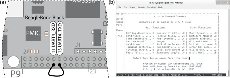
Figure 8-14 (a) Loopback testing the UART; (b) configuring the minicom program settings
molloyd@beaglebone:/lib/firmware$ ls *UART*
ADAFRUIT-UART1-00A0.dtbo  BB-UART1-00A0.dtbo  BB-UART4-RTSCTS-00A0.dtbo
ADAFRUIT-UART2-00A0.dtbo  BB-UART2-00A0.dtbo  BB-UART5-00A0.dtbo
ADAFRUIT-UART4-00A0.dtbo  BB-UART2-RTSCTS-00A0.dtbo
ADAFRUIT-UART5-00A0.dtbo  BB-UART4-00A0.dtbo
molloyd@beaglebone:/lib/firmware$ sudo su ‐c "echo BB‐UART4 > $SLOTS"
molloyd@beaglebone:/lib/firmware$ cat $SLOTS
...
 8: ff:P-O-L Override Board Name,00A0,Override Manuf,BB-UART4
When the overlay is loaded, the contents of the /dev directory now includes a new entry for ttyO4 (letter O, not zero). This is the “teletype” (terminal) device, which is a software interface that enables you to send and receive data on the UART. First, check the available terminal devices:
molloyd@beaglebone:/lib/firmware$ cd /dev
molloyd@beaglebone:/dev$ ls ttyO*
ttyO0 ttyO4To test the device, you can use the agetty (alternative getty) command or the minicom terminal emulator, both of which enable you to send and receive data on the ttyO4 device. The minicom program enables you to dynamically change the serial settings while it is executing (e.g., number of bits in a frame, number of stop bits, parity settings) by typing Ctrl+A followed by Z. Install and execute minicom using the following commands:
molloyd@beaglebone:~$ sudo apt‐get install minicom
...
molloyd@beaglebone:~$ minicom ‐b 9200 ‐o ‐D /dev/ttyO4

Welcome to minicom 2.6.1
OPTIONS: I18n
Compiled on Feb 11 2012, 18:45:56.
Port /dev/ttyO4
Press CTRL-A Z for help on special keys
At this point you should type Ctrl+A followed by Z and then E to turn on local Echo. Now when you press a key, you should see the following impact when you type:
tteessttiinngg 112233Whichever key you press is transmitted from the TXD output, and is also echoed on the console. When the character is received on the RXD input, it is then displayed on the console. Therefore, if you can see the characters appearing twice for the keys that you are pressing, then the simple UART test is working correctly. You can verify this by briefly disconnecting one end of the TXD‐RXD loopback wire, whereupon the key presses will only appear once.
The Arduino UART Example
The Arduino (www.arduino.cc) is a popular, low‐cost, and powerful microcontroller that can be a very useful companion controller for the BBB. The Arduino platform was designed as an introductory platform for embedded systems. It is programmed using the Arduino programming language, in the Arduino development environment, which are both designed to be as user‐friendly as possible. An in‐depth study of the Arduino is beyond the scope of this book, but it is a very suitable platform with which to test the UART functionality of the BBB. It can also be used to develop a first framework for BBB applications that distribute workload to other embedded systems while still maintaining high‐level control.
The Arduino is available in many different forms. However, an open‐hardware 3.3 V Arduino Pro Mini is chosen for this task for three reasons:
- The voltage levels are consistent with the BBB, which simplifies communication, as no logic‐level translation circuitry is required.
- It is a low‐cost, open‐hardware device (less than $10) that is only 1.3"× 0.7" (33 mm × 18 mm) in size.
- There is no USB input on the board (reducing size and cost), but it can be programmed using the same USB‐to‐Serial UART TTL 3.3 V cable discussed in Chapter 1.
Figure 8-15 illustrates the programming environment for the Arduino, and the program that is displayed can be used to test that the UART connection to the Arduino is working correctly. The code is available in the GitHub repository in /chp08/uart/arduino/BBBSerialEcho.ino. The Arduino platform uses the Arduino’s RXD and TXD pins to program the Arduino microcontroller, so a lot of spurious data is transmitted on these lines while it is being programmed.

Figure 8-15 The Arduino platform
The setup() function is called once when the program is started. It configures the serial port to use 9,600 baud with the 8N1 format. It also sets up an on‐board LED to be an output, in order to visually indicate interaction.
The loop() function will repeat as fast as it possibly can. In this case, it waits until serial data is available on the RXD pin. When it is, the LED is turned on, and a character is read in from the RXD pin. The character is then written to the TXD pin. The program sleeps for 100 ms to ensure that the LED flash is visible, before it is turned off again. The program then loops in preparation for the next character to be received on the RXD pin.
The Serial Monitor window can be opened in the Arduino development environment by pressing the button in the top right‐hand corner. Choose the baud rate that corresponds to that in the program code. When a string is entered in the text field and the Send button is pressed, the string is sent to the Arduino and the response should display in the text area.
Once you are certain that the Arduino program is working correctly, it is an ideal platform with which to test the BBB UART functionality.
BeagleBone to Arduino Serial Communication
The Arduino Pro Mini 3.3 V is used to test the UART communication capability of the BBB, first by using the minicom program and then by writing a C program to echo information to/from the Arduino. In the next section this is further developed to create a serial client/server command control framework.
Echoing the Minicom Program
The Arduino code from the last section has been modified slightly to increase the baud rate and remove the LED flash function, as shown in Listing 8‐9.
This program should be uploaded to the Arduino, where it will then execute, awaiting communication on its RXD pin. The next step is to connect the Arduino as illustrated in Figure 8-16, ensuring that the TXD pin on the BBB is connected to the RXD pin on the Arduino and that the RXD pin on the BBB is connected to the TXD pin on the Arduino.
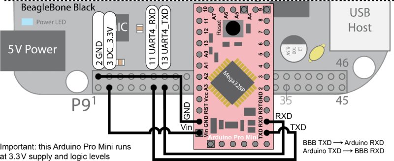
Figure 8-16 UART communication between the BBB and the Arduino Pro Mini 3.3 V
When you are modifying the Arduino source code and uploading it to the Arduino, you should disconnect the UART connection to the BBB each time, before connecting the USB‐to‐Serial UART TTL 3.3 V cable. Otherwise, the process of programming the Arduino will likely fail.
Once the Arduino is attached to the BBB, the next step is to open the minicom program and test the connection. The baud rate is set at 115,200 in the Arduino code, so the same setting must be passed to the minicom command. If the connection is displaying incorrect data, then reduce the baud rate to a lower rate, such as 57,600, 38,400, 19,200, or 9,600:
molloyd@beaglebone:~$ minicom ‐b 115200 ‐o ‐D /dev/ttyO4
Welcome to minicom 2.6.1
OPTIONS: I18n
Compiled on Feb 11 2012, 18:45:56.
Port /dev/ttyO4
Press CTRL-A Z for help on special keys
This string is being sent character by character to the Arduino
The Analog Discovery has an interpreter that can be used for analyzing serial data communication. The logic analyzer can be connected in parallel to the TXD and RXD lines in order to analyze the transfer of data from the BBB to the Arduino. An example of the resulting signals is displayed in Figure 8-17 when only the letter “A” is being transmitted. The start and stop bits can be observed, along with the eight‐bit data as it is sent, LSB first, from the BBB to the Arduino, at a sample bit‐period of 8.7 μs.
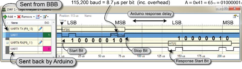
Figure 8-17 Analysis of the UART communication between the BBB and the Arduino Pro Mini 3.3 V
At a baud rate of 115,200, the effective byte rate will be somewhat lower, due to the overhead of transmitting start, stop, and parity bits. The Arduino response delay is the time it takes for the Arduino to read the character from its RXD input and transmit it back to its TXD output.
UART Echo Example in C
The next step is to write C code on the BBB that can communicate with the Arduino program. The Arduino code has been adapted slightly to reduce the baud rate to 9,600 in order ensure that signaling noise does not affect the data transfer, effectively isolating problems to the program code. All code is available in the /chp08/uart/uartEchoC GitHub repository directory.
The C program available in Listing 8‐10 sends a string to the Arduino and reads the responding echo. It uses the Linux termios library, which provides a general terminal interface that can control asynchronous communication ports.
This code uses the termios structure, setting flags to define the type of communication that should take place. The termios structure has the following members:
tcflag_t c_iflag: Sets the input modestcflag_t c_oflag: Sets the output modescflag_t c_cflag: Sets the control modestcflag_t c_lflag: Sets the local modescc_t c_cc[NCCS]: For special characters
A full description of the termios functionality and flag settings is available by typing man termios at the BBB console. The code in this section can be modified to create the following very useful BBB application.
UART Command Control of an Arduino
One method of overcoming the real‐time limitations of the BBB discussed in Chapter 1 is to outsource some of its workload to other embedded controllers, such as those provided by the Arduino, PIC, and Stellaris platforms. These embedded microcontrollers share common communication interfaces with the BBB that could be used for this task, including SPI, I2C, and the use of GPIO bit‐banging (manual serial communication using a GPIO by toggling its state in a user‐defined way). However, using a UART connection is probably the most straightforward, and it has the additional advantage that there can be some degree of physical distance between the two controllers. Table 8-6 lists some advantages and disadvantages of using a UART in comparison to using I2C or SPI.
Table 8-6 Advantages and Disadvantages of UART Communication
| ADVANTAGES | DISADVANTAGES |
| Simple, single‐wire transmission and single‐wire reception of data with error checking. | The typical maximum data rate is low compared to SPI (typically 460.8 kb/sec). |
| Easy interface for interconnecting embedded devices and desktop computers, etc., especially when that communication is external to the device and/or over a significant distance—some tens of feet. I2C and SPI are not suited for external/distance communication. | Because it is asynchronous, the clock on both devices must be accurate, particularly at higher baud rates. You should investigate CAN bus for high‐speed external asynchronous data transfer. |
| Can be directly interfaced to popular RS‐232 physical interfaces, enabling long‐distance communication (15 meters or greater). The longer the cable, the lower the speed. RS‐422/485 allows for 100‐meter runs at greater than 1 Mb/s. | UART settings need to be known in advance of the transfer, such as the baud rate, data size and parity checking type. |
The Arduino code in Listing 8‐9 has been adapted as shown in Listing 8‐11. The code is designed to expect two string commands, either “on” or “off.” If the program receives the “on” command on its RXD input, it will light the on‐board LED and respond on its TXD output with the response “LED On.” Similarly for the “off” command, it will turn the LED off and send the response “LED off.” If the command string is not recognized, it will simply echo the command string back to the sender. This program will continue to run on the Arduino forever.
The C program that is presented in Listing 8‐12 sends the command‐line argument, which is passed to the executable program over the UART connection to the Arduino at run time. It follows the same syntax as the echo example in the previous section, with the exception that the baud rate has been increased to 57,600 in both the C and Arduino program code.
When the code is executed, it will give the following output, with the LED on the Arduino turning on and off as expected:
molloyd@beaglebone:~/exploringbb/chp08/uart/uartC$ ./uart on
The following was read in [6]: LED On
molloyd@beaglebone:~/exploringbb/chp08/uart/uartC$ ./uart off
The following was read in [7]: LED Off
molloyd@beaglebone:~/exploringbb/chp08/uart/uartC$ ./uart HelloArduino
The following was read in [12]: HelloArduino
The transfer of data can be observed in Figure 8-18. The response time of the Arduino is less than the time taken to transfer the command and respond at 57,600 baud.
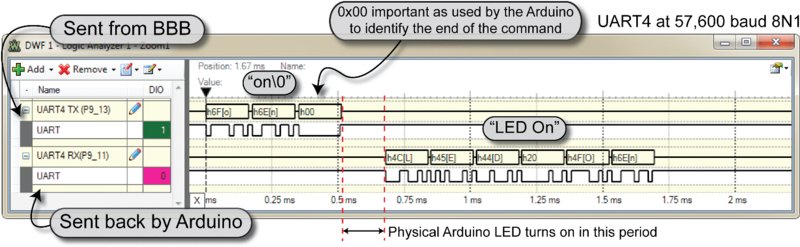
Figure 8-18 Sending the command “On�” to the Arduino and receiving the response string “LED On”
The performance of the code could be improved by defining a list of single‐byte commands and responses, in order to minimize data transfer time. In addition, it is worth mentioning that the multi‐call binary example discussed in Chapter 5 could be adapted to create single‐word Linux commands on the BBB that would execute directly on the Arduino.
This framework could be used to create a simple distributed embedded controller platform. An alternative would be to use the CAN bus controllers that are available on‐board the BBB and through third‐party capes. In Chapter 10, a network‐socket based framework is also introduced. It is a very powerful framework for interconnecting high‐level embedded computing platforms through the use of their networking interfaces.
Logic‐Level Translation
As noted throughout this chapter, it is important that you are cognizant of the voltage levels used in communicating with the BBB. If you connect a device that uses 5 V logic levels, then when the device is sending a high state to the BBB, it will apply a voltage of 5 V to the BBB’s input pins. This would likely permanently damage the BBB. Many embedded systems have overvoltage‐tolerant inputs, but the BBB does not. Therefore, logic‐level translation circuitry is required if you wish to connect the buses to 5 V or 1.8 V logic‐level circuits.
For unidirectional data buses, like four‐wire SPI, logic‐level translation can be achieved using a combination of diodes (using their ∼0.6 V forward‐voltage drop characteristic) combined with resistors, or transistors. However, bidirectional data buses like the I2C bus are more complex because the level must be translated in both directions on a single line. This requires circuits that use devices such as N‐channel MOSFETs (e.g., the BSS138). They are available in surface‐mounted packages and, unfortunately, there are very few through‐hole alternatives. Fortunately, this is a common problem and there are straightforward unidirectional and bidirectional breakout board solutions available from several suppliers, including the following:
- Sparkfun Logic Level Converter Bi‐directional (BOB‐12009), which uses the BSS138 MOSFET (∼$3)
- Adafruit Four‐channel Bi‐directional Level Shifter (ID:757), which uses the BSS138 MOSFET (1.8 V to 10 V shifting)(∼$4)
- Adafruit Eight‐channel Bi‐directional Logic‐level Converter (ID:395), which uses the TI TXB0108 voltage‐level translator that auto senses direction (1.2 to 3.6 V or 1.65 to 5.5 V translation), but it does not work well with I2C due to the pull‐up resistors required (∼$8). However, it can switch at frequencies greater than 10 MHz.
- Watterott Four‐channel Level Shifter (20110451), which uses the BSS138 MOSFET (∼$3)
Some of these products are displayed in Figure 8-19. With the exception of the Adafruit eight‐channel converter, they all use BSS138 MOSFETs. A small test was performed to check the switching frequency of these devices, as displayed in Figure 8-20, and it is clear from the oscilloscope traces that there are data‐switching performance limitations when using these devices.
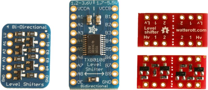
Figure 8-19 Adafruit four‐channel, Adafruit eight‐channel, and Watterott four‐channel logic‐level translators
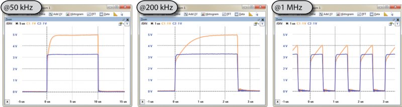
Figure 8-20 Switching BSS138‐based translators from 3.3 V to 5 V logic levels at 50 kHz, 200 kHz, and 1 MHz
The logic‐level translation boards solve the problem that is mentioned several times during this chapter, as a traditional 5 V Arduino can now be connected to the BBB for UART communication using the circuit that is illustrated in Figure 8-21. The BBB 3.3 V supply, TXD, and RXD pins are connected to the Lv, 1, and 2 connections, respectively, on the logic‐level translator board. On the other side of the logic‐level translator, the Arduino 5 V supply, RXD, and TXD pins are connected to the Hv, 1, and 2 connection pins, respectively. The grounds of the BBB and Arduino are also tied together.
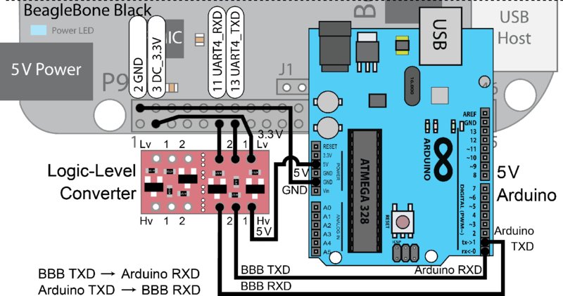
Figure 8-21 Connecting a 5 V Arduino UART to the BBB UART using a logic‐level converter
The application that is used to provide UART command control of the Arduino now works with this 5 V Arduino. For further information on logic‐level shifting techniques in I2C‐bus design, see the application notes from NXP (AN97055), which is linked on the chapter web page and also available at tiny.cc/ebb806.
Summary
After completing this chapter, you should be able to do the following:
- Describe the most commonly used buses or interfaces that are available on the BBB, and choose the correct bus to use for your application.
- Configure the BBB to enable I2C, SPI, and UART capabilities.
- Attach circuits to the BBB that interface to its I2C bus, and use the Linux I2C‐Tools to communicate with those circuits.
- Build circuits that interface to the SPI bus using shift registers, and write C code that controls low‐level SPI communication.
- Write C code that interfaces to, and C++ code that “wraps” the functionality of devices attached to the I2C and SPI buses.
- Communicate between UART devices using both Linux tools and custom C code.
- Build a basic distributed system that uses UART connections to the Arduino microcontroller to “outsource” workload.
- Add logic‐level translation circuitry to your circuits in order to communicate between devices with different logic‐level voltages.
Further Reading
Documents and links for further reading have been listed throughout this chapter, but here are some further reference documents:
- The I2C Manual, Jean‐Marc Irazabal and Steve Blozis, Philips Semiconductors, TecForum at DesignCon 2003 in San Jose, CA, on January 27, 2003, at
tiny.cc/ebb805. - The Linux I2C Subsystem, at
i2c.wiki.kernel.org. - Serial Programming Guide for POSIX Operating Systems, 5th ed., Michael R. Sweet, 1994‐99, at
tiny.cc/ebb803. - Serial Programming HOWTO, Gary Frerking, Revision 1.01, at
tiny.cc/ebb804.