3
Arithmetic Basics
3.1 Introduction
The choice of arithmetic has always been a key aspect for DSP implementation as it not only affects algorithmic performance, but also can impact system performance criteria, specifically area, speed and power consumption. This usually centers around the choice of a floating-point or a fixed-point realization, and in the latter case, a detailed study is needed to determine the minimal wordlength needed to achieve the required performance. However, with FPGA platforms, the choice of arithmetic can have a much wider impact on the performance as the system designer can get a much more direct return from any gains in terms of reducing complexity. This will either reduce the cost or improve the performance in a similar way to an SoC designer.
A key requirement of DSP implementations is the availability of suitable processing elements, specifically adders and multipliers; however, many DSP algorithms (e.g. adaptive filters) also require dedicated hardware for performing division and square roots. The realization of these functions, and indeed the choice of number systems, can have a major impact on hardware implementation quality. For example, it is well known that different DSP application domains (e.g. image processing, radar and speech) can have different levels of bit toggling not only in terms of the number of transitions, but also in the toggling of specific bits (Chandrakasan and Brodersen 1996). More specifically, the signed bit in speech input can toggle quite often, as data oscillates around zero, whereas in image processing the input typically is all positive. In addition, different applications can have different toggling activity in their lower significant bits. This can have a major impact in reducing dynamic power consumption.
For these reasons, it is important that some aspects of computer arithmetic are covered, specifically number representation as well as the implementation choices for some common arithmetic functions, namely adders and multipliers. However, these are not covered in great detail as the reality is that in the case of addition and multiplication, dedicated hardware has been available for some time on FPGA and thus for many applications the lowest-area, fastest- speed and lowest-power implementations will be based on these hardware elements. As division and square root operations are required in some DSP functions, it is deemed important that they are covered here. As dynamic range is also important, the data representations, namely fixed-point and floating-point, are also seen as critical.
The chapter is organized as follows. In Section 3.2 some basics of computer arithmetic are covered, including the various forms of number representations as well as an introduction to fixed- and floating-point arithmetic. This is followed by a brief introduction to adder and multiplier structures in Section 3.3. Of course, alternative representations also need some consideration so signed digit number representation (SDNR), logarithmic number representations (LNS), residue number representations (RNS), and coordinate rotation digital computer (CORDIC) are considered in Section 3.4. Dividers and circuits for square root are then covered in Sections 3.5 and 3.6, respectively. Some discussion of the choice between fixed-point and floating-point arithmetic for FPGA is given in Section 3.7. In Section 3.8 some conclusions are given and followed by a discussion of some key issues.
3.2 Number Representations
From our early years we are taught to compute in decimal, but the evolution of transistors implies the adoption of binary number systems as a more natural representation for DSP systems. This section starts with a basic treatment of conventional number systems, namely signed magnitude and one’s complement, but concentrates on two’s complement. Alternative number systems are briefly reviewed later as indicated in the introduction, as they have been applied in some FPGA-based DSP systems.
If x is an (n + 1)-bit unsigned number, then the unsigned representation

applies, where xi is the ith binary bit of n and x0 and xn are least significant bit (lsb) and most significant bit (msb) respectively. The binary value is converted to decimal by scaling each bit to the relevant significance as shown below, where 1110 is converted to 14:
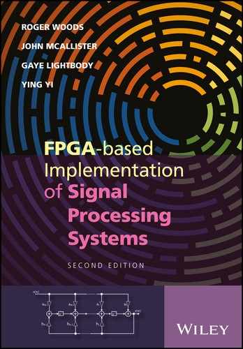
Decimal to binary conversion is done by successive divisions by 2. For the expression D = (x3x2x1x0)2 = x323 + x222 + x121 + x0, we successively divide by 2:
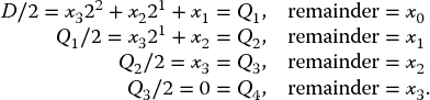
So if 14 is converted to binary, this is done as follows:
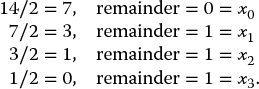
In signed magnitude systems, the n − 1 lower significant bits represent the magnitude, and the msb, xn, bit represents the sign. This is best represented pictorially in Figure 3.1(a), which gives the number wheel representation for a four-bit word. In the signed magnitude notation, the magnitude of the word is decided by the three lower significant bits, and the sign determined by the sign bit, or msb. However, this representation presents a number of problems. First, there are two representations of 0 which must be resolved by any hardware system, particularly if 0 is used to trigger any event (e.g. checking equality of numbers). As equality is normally achieved by checking bit-by-bit, this complicates the hardware. Lastly, operations such as subtraction are more complex, as there is no way to check the sign of the resulting value, without checking the size of the numbers and organizing accordingly. This creates overhead in hardware realization and prohibits the number system’s use in practical systems. Figure 3.1 Number wheel representation of four-bit numbers In one's-complement systems, the assignment of the bits is done differently. It is based around representing the negative version of the numbers as the inverse or one's complement of the original number. This is achieved by inverting the individual bits, which in practice can easily be achieved through the use of an inverter. The conversion for an n-bit word is given by
and the pictorial representation for a four-bit binary word is given in Figure 3.1(b). The problem still exists of two representations of 0. Also, a correction needs to be carried out when performing one's complement subtraction (Omondi 1994). Once again, the need for special treatment of 0 is prohibitive from an implementation perspective. In two's-complement systems, the inverse of the number is obtained by inverting the bits of the original word and adding 1. The conversion is given by
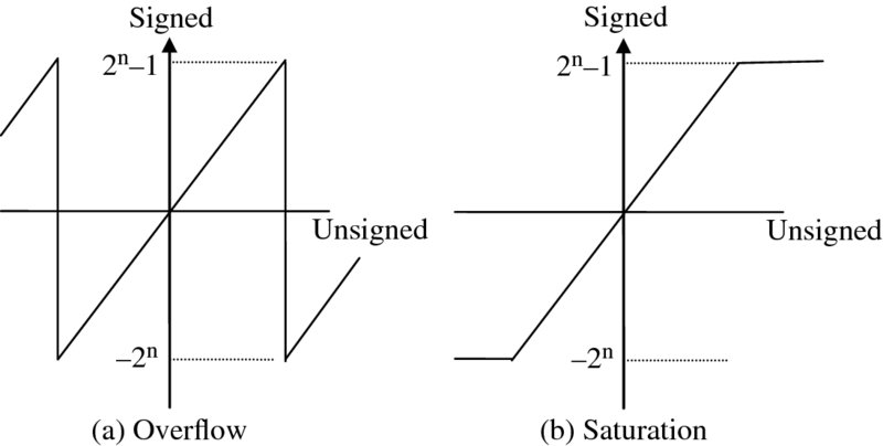
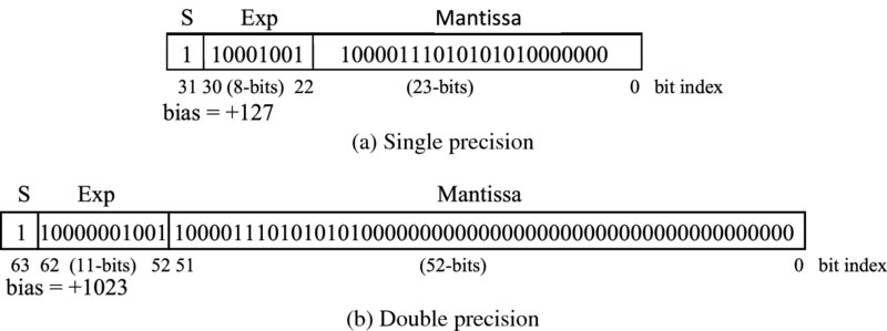
and the pictorial representation for a four-bit binary word given in Figure 3.1(c). Whilst this may seem less intuitively obvious than the previous two approaches, it has a number of advantages: there is a single representation for 0, addition and more importantly subtraction can be performed readily in hardware and if the number stays within range, overflow can be ignored in the computation. For these reasons, two's complement has become the dominant number system representation. This representation therefore efficiently translates into efficient hardware structures for the core arithmetic functions and means that addition and subtraction is easily implemented. As will be seen later, two's complement multiplication is a little more complicated but the single representation of 0 is the differentiator. As will be seen in the next section, the digital circuitry naturally falls out from this. By applying different weighting, a number of other binary codes can be applied as shown in Table 3.1. The following codes are usually called binary coded decimal (BCD). The 2421 is a nine's complement code, i.e. 5 is the inverse of 4, 6 is the inverse of 3, etc. With the Gray code, successive decimal digits differ by exactly one bit. This coding styles tends to be used in low-power applications where the aim is to reduce the number of transitions (see Chapter 13). Table 3.1 BCD codes Up until now, we have only considered integer representations and not considered the real representations which we will encounter in practical DSP applications. A widely used format for representing and storing numerical binary data is the fixed-point format, where an integer value x represented by xm + n − 1, xm + n − 2, …, x0 is mapped such that xm + n − 1, xm + n − 2, …, xn represents the integer part of the number and the expression, xn − 1, xn − 2, …, x0 represents the fractional part of the number. This is the interpretation placed on the number system by the user and generally in DSP systems, users represent input data, say x(n), and output data, y(n), as integer values and coefficient word values as fractional so as to maintain the best dynamic range in the internal calculations. The key issue when choosing a fixed-point representation is to best use the dynamic range in the computation. Scaling can be applied to cover the worst-case scenario, but this will usually result in poor dynamic range. Adjusting to get the best usage of the dynamic range usually means that overflow will occur in some cases and additional circuitry has to be implemented to cope with this condition; this is particularly problematic in two's complement as overflow results in an “overflowed” value of completely different sign to the previous value. This can be avoided by introducing saturation circuitry to preserve the worst-case negative or positive overflow, but this has a nonlinear impact on performance and needs further investigation. The impact of overflow in two's complement is indicated by the sawtooth representation in Figure 3.2(a). If we consider the four-bit representation represented earlier in Figure 3.1 and look at the addition of 7 (0111) and 1(0001), then we see that this will give 8 (1000) in unsigned binary, but of course this represents − 8 in 2’s complement which represents the worse possible representation. One approach is to introduce circuitry which will saturate the output to the nearest possible value, i.e. 7 (0111). This is demonstrated in Figure 3.2(b), but the impact is to introduce a nonlinear impact to the DSP operation which needs to be evaluated. Figure 3.2 Impact of overflow in two's complement This issue is usually catered for in the high-level modeling stage using tools such as those from MATLAB® or LabVIEW. Typically the designer is able to start with a floating-point representation and then use a fixed-point library to evaluate the performance. At this stage, any impact of overflow can be investigated. A FPGA-based solution may have timing problems as a result of any additional circuitry introduced for saturation. One conclusion that the reader might draw is that fixed-point is more trouble than it is worth, but fixed-point implementations are particularly attractive for FPGA implementations (and some DSP microprocessor implementations), as word size translates directly to silicon area. Moreover, a number of optimizations are available that make fixed-point extremely attractive; these are explored in later chapters. Floating-point representations provide a much more extensive means for providing real number representations and tend to be used extensively in scientific computation applications, but also increasingly in DSP applications. In floating-point, the aim is to represent the real number using a sign (S), exponent (Exp) and mantissa (M), as shown in Figure 3.3. The most widely used form of floating-point is the IEEE Standard for Binary Floating-Point Arithmetic (IEEE 754). This specifies four formats: Figure 3.3 Floating-point representations The single-precision format is a 32-bit representation where 1 bit is used for S, 8 bits for Exp and 23 bits for M. This is illustrated in Figure 3.3(a) and allows the representation of the number x where x is created by 2Exp − 127 × M as the exponent is represented as unsigned, giving a single-extended number of approximately ± 1038.52. The double-precision format is a simple extension of the concept to 64 bits, allowing a range of ± 10308.25, and is illustrated in Figure 3.3(b); the main difference between this and single precision being the offset added to the exponent and the addition of zero padding for the mantissa. The following simple example shows how a real number, − 1082.5674 is converted into IEEE 754 floating-point format. It can be determined that S = 1 as the number is negative. The number (1082) is converted to binary by successive division (see earlier), giving 10000111010. The fractional part (0.65625) is computed in the same way as above, giving 10101. The parts are combined to give the value 10000111010.10101. The radix point is moved left, to leave a single 1 on the left, giving 1.000011101010101 × 210. Filling with 0s to get the 23-bit mantissa gives the value 10000111010101010000000. In this value the exponent is 10 and, with the 32-bit IEEE 754 format bias of 127, we have 137 which is given as 10001001 in binary (giving the representation in Figure 3.3(a)).3.2.1 Signed Magnitude
3.2.2 One’s Complement
![]()
3.2.3 Two’s Complement
![]()
3.2.4 Binary Coded Decimal
BCD
Decimal
8421
2421
Gray
0
0000
0000
0000
1
0001
0001
0001
2
0010
0010
0011
3
0011
0011
0010
4
0100
0100
0110
5
0101
1011
1110
6
0110
1100
1010
7
0111
1101
1011
8
1000
1110
1001
9
1001
1111
1000
3.2.5 Fixed-Point Representation
3.2.6 Floating-Point Representation
3.3 Arithmetic Operations
This section looks at the implementation of various arithmetic functions, including addition and multiplication but also division and square root. As the emphasis is on FPGA implementation which comprises on-board adders and multipliers, the book concentrates on using these constructions, particularly fixed-point realizations. A brief description of a floating-point adder is given in the following section.
3.3.1 Adders
Addition of two numbers A and B to produce a result S,
is a common function in computing systems and central to many DSP systems. Indeed, it is a key operation and also forms the basic of multiplication which is, in effect, a series of shifted additions.
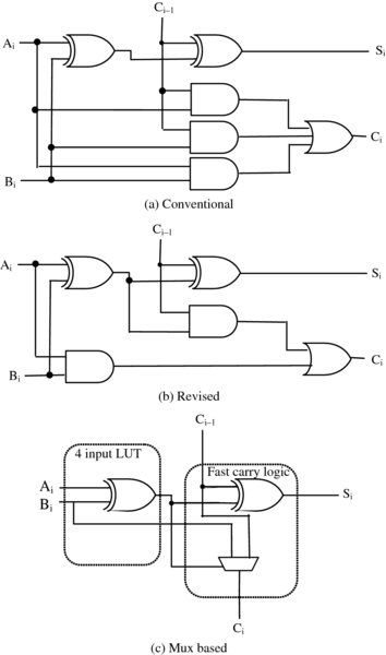
Figure 3.4 One-bit adder structure
Table 3.2 Truth table for a one-bit adder
| Inputs | Outputs | ||||
| A | B | Ci − 1 | Si | Ci | |
| 0 | 0 | 0 | 0 | 0 | |
| 0 | 0 | 1 | 1 | 0 | |
| 0 | 1 | 0 | 1 | 0 | |
Ci = Ci − 1 |
0 | 1 | 1 | 0 | 1 |
| 1 | 0 | 0 | 1 | 0 | |
| 1 | 0 | 1 | 0 | 1 | |
| 1 | 1 | 0 | 0 | 1 | |
| 1 | 1 | 1 | 1 | 1 | |
A single-bit addition function is given in Table 3.2, and the resulting implementation in Figure 3.4(a). This form comes directly from solving the one-bit adder truth table leading to
and the logic gate implementation of Figure 3.4(a).
By manipulating the expression for Ci, we can generate the alternative expression
This has the advantage of sharing the expression Ai⊕Bi between both the Si and Ci expressions, saving one gate but as Figure 3.4(b) illustrates, at the cost of an increased gate delay.
The truth table can also be interpreted as follows: when Ai = Bi, then Ci = Bi and Si = Ci − 1; and when ![]() , then Ci = Ci − 1 and
, then Ci = Ci − 1 and ![]() . This implies a multiplexer for the generation of the carry and, by cleverly using Ai⊕Bi (already generated in order to develop Si), very little additional cost is required. This is the preferred construction for FPGA vendors as indicated by the partition of the adder cell in Figure 3.4(c). By providing a dedicated EXOR and mux logic, the adder cell can then be built using a LUT to generate the additional EXOR function.
. This implies a multiplexer for the generation of the carry and, by cleverly using Ai⊕Bi (already generated in order to develop Si), very little additional cost is required. This is the preferred construction for FPGA vendors as indicated by the partition of the adder cell in Figure 3.4(c). By providing a dedicated EXOR and mux logic, the adder cell can then be built using a LUT to generate the additional EXOR function.
3.3.2 Adders and Subtracters
Of course, this only represents a single-bit addition, but we need to add words rather than just bits. This can be achieved by chaining one-bit adders together to form a word-level adder as shown in Figure 3.5. This represents the simplest but most area-efficient adder structure. However, the main limitation is the time required to compute the word-level addition which is determined by the time for the carry to propagate from the lsb to the msb. As wordlength increases, this becomes prohibitive.
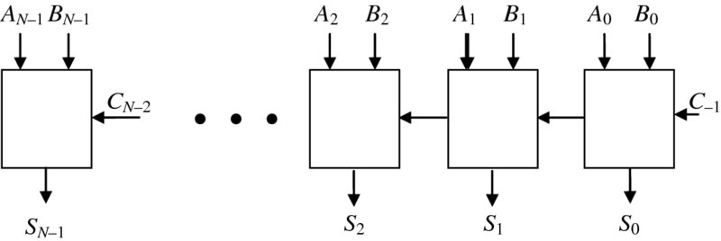
Figure 3.5 n-bit adder structure
For this reason, there has been a considerable body of detailed investigations in alternative adder structures to improve speed. A wide range of adder structures have been developed including the carry lookahead adder (CLA) and conditional sum adder (CSA), to name but a few (Omondi 1994). In most cases the structures compromise architecture regularity and area efficiency to overcome the carry limitation.
Carry Lookahead Adder
In the CLA adder, the carry expression given in equation (3.7) is unrolled many times, making the final carry dependent only on the initial value. This can be demonstrated by defining a generate function, Gi, as Gi = Ai · Bi, and a propagate function, Pi, as Pi = Ai⊕Bi. Thus we can rewrite equations (3.5) and (3.7) as
By performing a series of substitutions on equation (3.9), we can get an expression for the carry out of the fourth addition, namely C3, which only depends on the carry in of the first adder C− 1, as follows:
Adder Comparisons
It is clear from the expressions in equations (3.10)–(3.13) that this results in a very expensive adder structure due to this unrolling. If we use the gate model by Omondi (1994), where any gate delay is given by T and gate cost or area is defined in terms of 2n (a two-input AND gates is 2, a three-input AND gates is 3, etc.) and EXORs count as double (i.e. 4n), then this allows us to generate a reasonable technology-independent model of computation. In this case, the critical path is given as 4T, which is only one more delay than that for the one-bit adder of Figure 3.4(b).
For the CRA adder structure in Figure 3.4(b), it can be seen that the adder complexity is determined by two 2-input AND gates (cost 2 × 2), i.e. 4, and one 2-input NOR gate, i.e. 2, and then two 2-input EXOR gates, which is 2 × 4 (remember there is a double cost for EXOR gates). This gives a complexity of 14, which if we multiply up by 16 gives a complexity of 224 as shown in the first line of Table 3.2. The delay of the first adder cell is 3T, followed by n − 2 delays of 2T and a final delay of T, this giving an average of 2nT delays, i.e. 32T.
If we unloop the computation of equations (3.10)–(3.13) a total of 15 times, we can get a structure with the same gate delay of 4T, but with a very large gate cost i.e. 1264, which is impractical. For this reason, a merger of the CLA technique with the ripple carry structure is preferred. This can be achieved either in the form of the block CLA with inter-block ripple (RCLA) which in effect performs a four-bit addition using a CLA and organizes the structure as a CRA (see Figure 3.6(a)), or a block CLA with intra-group, carry ripple (BCLA) which uses the CLA for the computation of the carry and then uses the lower-cost CRA for the reset of the addition (see Figure 3.6(b)).
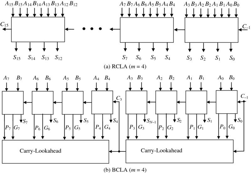
Figure 3.6 Alternative CLA structures
These circuits also have varying critical paths as indicated in Table 3.3. A detailed examination of the CLA circuit reveals that it takes 3T to produce the first carry, then 2T for each of the subsequent stages to produce their carry as the Gi terms will have been produced, and finally 2T to create the carry in the final CLA block. This gives a delay for the 16-bit RCLA of 10T.
Table 3.3 16-bit adder comparisons
| Adder type | Time (gate delay) | Cost (CUs) | Performance |
| CRA (Figure 3.5) | 32 | 224 | 0.72 |
| Pure CLA | 4 | 1264 | 0.51 |
| RCLA (m = 4) (Figure 3.6(a)) | 10 | 336 | 0.34 |
| BCLA (m = 4) (Figure 3.6(b)) | 14 | 300 | 0.42 |
The performance represents an estimation of speed against gate cost given as cost unit (CU) and is given by cost multiplied by time divided by 10, 000. Of course, this will only come in to play when all circuits meet the timing requirements, which is unusual as it is normally speed that dominates with choice of lowest area then coming as a second measure. However, it is useful in showing some kind of performance measure.
3.3.3 Adder Final Remarks
To a large extent, the variety of different adder structures trade off gate complexity with system regularity, as many of the techniques end up with structures that are much less regular. The aim of much of the research which took place in the 1970s and 1980s was to develop higher-speed structures where transistor switching speed was the dominant feature. However, the analysis in the introduction to this book indicates the key importance of interconnect, and somewhat reduces the impact of using specialist adder structures. Another critical consideration for FPGAs is the importance of being able to scale adder word sizes with application need, and in doing so, offer a linear scale in terms of performance reduction. For this reason, the ripple-carry adder has great appeal in FPGAs and is offered in many of the FPGA structures as a dedicated resource (see Chapter 5).
In papers from the 1990s and early 2000s there was an active debate in terms of adder structure (Hauck et al. 2000; Xing and Yu ). However, it is clear that, even for adder trees that are commonly used to sum numerous multiplication operations as commonly occurs in DSP applications, the analysis outlined in (Hoe et al. 2011) supports the use of the dedicated CRA adder structures on FPGAs.
3.3.4 Multipliers
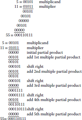
Multiplication can be simply performed through a series of additions. Consider the example below, which illustrates how the simple multiplication of 5 by 11 is carried out in binary. The usual procedure in computer arithmetic is to align the data in a vertical line and shift right rather than shift left, as shown below. However, rather than perform one single addition at the end to add up all the multiples, each multiple is added to an ongoing product called a partial product. This means that every step in the computation equates to the generation of the multiples using an AND gate and the use of an adder to compute the partial product.
A parallel addition can be computed by performing additions at each stage of the multiplication operation. This means that the speed of operation will be defined by the time required to compute the number of additions defined by the multiplicand. However, if the adder structures of Figure 3.5 were to be used, this would result in a very slow multiplier circuit. Use of alternative fast adders structures (some of which were highlighted in Table 3.3) would result in improved performance but this would be a considerable additional cost.
Fast Multipliers
The received wisdom in speeding up multiplications is to either speed up the addition or reduce the number of additions. The latter is achieved by recoding the multiplicand, commonly termed Booth’s encoding (discussed shortly). However, increasing the addition speed is achieved by exploiting the carry-save adder structure of Figure 3.7. In conventional addition, the aim is to reduce (or compress) two input numbers into a single output. In multiplication, the aim is to reduce multiple numbers, i.e. multiplicands, down to a single output value. The carry-save adder is a highly efficient structure that allows us to compress three inputs down to two outputs at the cost of a CRA addition but with the speed of the individual cells given in Figure 3.4(b) or (c), namely two or three gate delays.
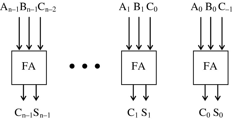
Figure 3.7 Carry-save adder
Thus it is possible to create a carry-save array multiplier as shown in Figure 3.8. An addition is required at each stage, but this is a much faster, smaller CSA addition, allowing a final sum and carry to be quickly generated. A final adder termed a carry propagation adder (CPA) is then used to compute the final addition using one of the fast addition circuits from earlier.
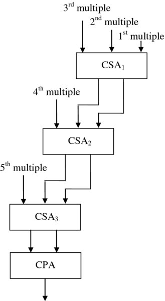
Figure 3.8 Carry-save array multiplier
Even though each addition stage is reduced to two or three gate delays, the speed of the multiplier is then determined by the number of stages. As the word size m grows, the number of stages is then given as m − 2. This limitation is overcome in a class of multipliers known as Wallace tree multipliers (Wallace 1964), which allows the addition steps to be performed in parallel. An example is shown in Figure 3.9.
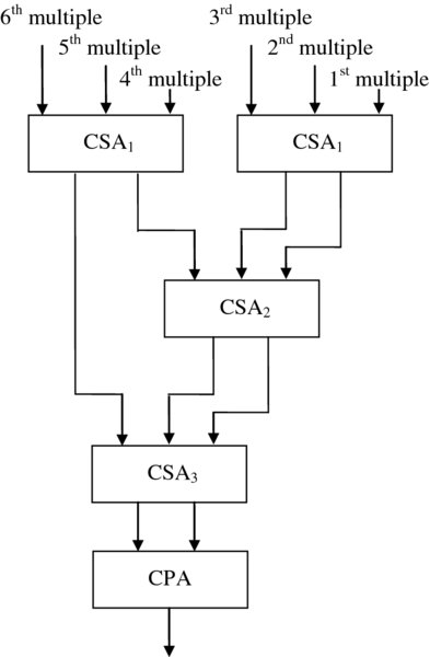
Figure 3.9 Wallace tree multiplier
As the function of the carry-save adder is to compress three words to two words, this means that if n is the input wordlength, then after each stage, the words are represented as 3k + l, where 0 ⩽ l ⩽ 2. This means that the final sum and carry values are produced after log 1.5n rather than n − 1 stages as with the carry-save array multiplier, resulting in a much faster implementation.
Booth Encoding
It was indicated earlier that the other way to improve the speed of a multiplier was to reduce the number of additions performed in the multiplications. At first thought, this does not seem obvious as the number of additions is determined by the multiplicand (MD). However, it is possible to encode the binary input in such a way as to reduce the number of additions by two, by exploiting the fact that an adder can easily implement a subtraction.
The scheme is highlighted in Table 3.4 and shows that by examining three bits of the multiplier (MR), namely MRi + 1, MRi and MRi − 1, it is is possible to reduce two bit operations down to one operation, either an addition or subtraction. This requires adding to the multiplier the necessary conversion circuitry to detect these sequences. This is known as the modified Booth’s algorithm. The overall result is that the number of additions can be halved.
Table 3.4 Modified Booth’s algorithm
| MRi + 1, i | MRi − 1 | Action |
| 00 | 0 | Shift partial product by 2 places |
| 00 | 1 | Add MD and shift partial product by 2 places |
| 01 | 0 | Add MD and shift partial product by 2 places |
| 01 | 1 | Add 2 × MD and shift partial product by 2 places |
| 10 | 0 | Subtract 2 × MD and shift partial product by 2 places |
| 10 | 1 | Subtract MD and shift partial product by 2 places |
| 11 | 0 | Subtract MD and shift partial product by 2 places |
| 11 | 1 | Shift partial product by 2 places |
The common philosophy for fast additions is to combine the Booth encoding scheme with Wallace tree multipliers to produce a faster multiplier implementation. In Yeh and Jen (2000), the authors present an approach for a high-speed Booth encoded parallel multiplier using a new modified Booth encoding scheme to improve performance and a multiple-level conditional-sum adder for the CPA.
3.4 Alternative Number Representations
Over the years, a number of schemes have emerged for either faster or lower-cost implementation of arithmetic processing functions. These have included SDNR (Avizienis 1961), LNS (Muller 2005), RNS (Soderstrand et al. 1986) and the CORDIC representation (Voider 1959; Walther 1971). Some of these have been used in FPGA designs specifically for floating-point implementations.
3.4.1 Signed Digit Number Representation
SDNRs were originally developed by Avizienis (1961) as a means to break carry propagation chains in arithmetic operations. In SDNR, each digit is associated with a sign, positive or negative. Typically, the digits are represented in balanced form and drawn from a range − k to (b − 1) − k, where b is the number base and typically ![]() . For balanced ternary which best matches conventional binary, this gives a digit set for x where x ∈ ( − 1, 0, 1), or strictly speaking (1,0,
. For balanced ternary which best matches conventional binary, this gives a digit set for x where x ∈ ( − 1, 0, 1), or strictly speaking (1,0,![]() ) where
) where ![]() represents − 1. This is known as signed binary number representation (SBNR), and the digits are typically encoded by two bits, namely a sign bit, xs, and a magnitude bit, xm, as shown in Table 3.5. Avizienis (1961) was able to demonstrate how such a number system could be used for performing parallel addition without the need for carry propagation (shown for an SBNR adder in Figure 3.10), effectively breaking the carry propagation chain.
represents − 1. This is known as signed binary number representation (SBNR), and the digits are typically encoded by two bits, namely a sign bit, xs, and a magnitude bit, xm, as shown in Table 3.5. Avizienis (1961) was able to demonstrate how such a number system could be used for performing parallel addition without the need for carry propagation (shown for an SBNR adder in Figure 3.10), effectively breaking the carry propagation chain.
![Diagram of SBNR adder with two FAs where the output from one FA goes as input to the 2nd FA the inputs are A0
+A0
-B0
+B0
- and 0 and the output signals are S0
+S0
- [-1,0] as final output.](http://images-20200215.ebookreading.net/13/1/1/9781119077954/9781119077954__fpga-based-implementation-of__9781119077954__images__c03f010.jpg)
Figure 3.10 SBNR adder
Table 3.5 SDNR encoding
| SDNR representations | ||||
| SDNR digit | Sig-and-mag | + / − coding | ||
| x | xs | xm | x+ | x− |
| 0 | 0 | 0 | 0 | 1 |
| 1 | 0 | 1 | 1 | 0 |
| 0 | 1 | 0 | 1 | |
| 0 or X | 1 | 0 | 1 | 0 |
A more interesting assignment is the ( +, −) scheme where an SBNR digit is encoded as (x+, x−), where x = x+ + (x− − 1). Alternatively, this can be thought of as x− = 0 implying − 1, x− = 1 implying 0, x+ = 0 implying 0, and x+ = 1 implying 1. The key advantage of this approach is that it provides the ability to construct generalized SBNR adders from conventional adder blocks.
This technique was effectively exploited to allow the design of high- speed circuits for arithmetic processing and digital filtering (Knowles et al. 1989) and also for Viterbi decoding (Andrews 1986). In many DSP applications such as filtering, the filter is created with coefficient values such that for fixed-point DSP realizations, the top part of the output word is then required after truncation. If conventional pipelining is used, it will take several cycles for the first useful bit to be generated, seemingly defeating the purpose of using pipelining in the first place.
Using SBNR arithmetic, it is possible to generate the result msb or strictly most significant digit (msd) first, thereby allowing the computation to progress much more quickly. In older technologies where speed was at a premium, this was an important differentiator and the work suggested an order-of-magnitude improvement in throughput rate. Of course, the redundant representation had to be converted back to binary, but several techniques were developed to achieve this (Sklansky 1960).
With evolution in silicon processes, SBNR representations are now being overlooked in FPGA design as it requires use of the programmable logic hardware and is relatively inefficient, whereas conventional implementations are able to use the dedicated fast adder logic which will be seen in later chapters. However, its concept is very closely related to binary encoding such as Booth’s encoding. There are many fixed-point applications where these number conventions can be applied to reduce the overall hardware cost whilst increasing speed.
3.4.2 Logarithmic Number Systems
The argument for LNS is that it provides a similar range and precision to floating-point but offers advantages in complexity over some floating-point applications. For example, multiplication and division are simplified to fixed-point addition and subtraction, respectively (Haselman et al. 2005; Tichy et al. 2006).
If we consider that a floating-point number is represented by
then logarithmic numbers can be viewed as a specific case of floating-point numbers where the mantissa is always 1, and the exponent has a fractional part (Koren 2002). The logarithmic equivalent, L, is then described as
where SA is the sign bit which signifies the sign of the whole number and ExpA is a two's complement fixed-point number where the negative numbers represent values less than 1.0. In this way, LNS numbers can represent both very large and very small numbers. Typically, logarithmic numbers will have a format where two bits are used for the flag bit (to code for zero, plus/minus infinity, and Not a Number (NaN (Detrey and de Dinechin 2003)), and then k bits and l bits represent the integer and fraction respectively (Haselman et al. 2005).
A major advantage of the LNS is that multiplication and division in the linear domain ares replaced by addition or subtraction in the log domain:
However, the operations of addition and subtraction are more complex. In Collange et al. (2006), the development of an LNS floating-point library is described and it is shown how it can be applied to some arithmetic functions and graphics applications.
However, LNS has only really established itself in small niche markets, whereas floating-point number systems have become a standard. The main advantage comes from computing a considerable number of operations in the algorithmic domain where the advantages are seen as conversion is problem. Conversions are not exact and error can accumulate for multiple conversions (Haselman et al. 2005). Thus whilst there has been some floating-point library developments, FPGA implementations have not been very common.
3.4.3 Residue Number Systems
RNS representations are useful in processing large integer values and therefore have application in computer arithmetic systems, as well as in some DSP applications (see later), where there is a need to perform large integer computations. In RNS, an integer is converted into a number which is an N-tuple of smaller integers called moduli, given by (mN, mN − 1, …, m1). An integer X is represented in RNS by an N-tuple (xN, xN − 1, …, x1), where Xi is a non-negative integer, satisfying
where qi is the largest integer such that 0 ⩽ qi ⩽ (mi − 1) and the value xi is known as the residue of X modulo mi. The main advantage of RNS is that additions, subtractions and multiplications are inherently carry-free due to the translation into the format. Unfortunately, other arithmetic operations such as division, comparison and sign detection are very slow and this has hindered the broader application of RNS. For this reason, the work has mostly been applied to DSP operations that involve a lot of multiplications and additions such as FIR filtering (Meyer-Baese et al. ) and transforms such as the FFT and DCT (Soderstrand et al. 1986).
Albicocco et al. (2014) suggest that in the early days RNS was used to reach the maximum performance in speed, but now it is used primarily to obtain power efficiency and speed–power trade-offs and for reliable systems where redundant RNS are used. It would seem that the number system is suffering the same consequences as SDNRs as dedicated, high-speed computer arithmetic has now emerged in FPGA technology, making a strong case for using conventional arithmetic.
3.4.4 CORDIC
The unified CORDIC algorithm was originally proposed by Voider (1959) and is used in DSP applications for functions such as those shown in Table 3.6. It can operate in one of three configurations (linear, circular and hyperbolic) and in one of two modes (rotation and vectoring) in those configurations. In rotation, the input vector is rotated by a specified angle; in vectoring, the algorithm rotates the input vector to the x-axis while recording the angle of rotation required. This makes it attractive for computing trigonometric operations such as sine and cosine and also for multiplying or dividing numbers.
Table 3.6 CORDIC functions
| Configuration | Rotation | Vectoring |
| Linear | Y = X × Y | Y = X/Y |
Hyperbolic |
X = cosh (X) | Z = arctanh |
| Y = sinh (Y) | ||
Circular |
X = cos (X) | Z = arctanh(Y) |
| Y = sin (Y) | X = sqr(X2 + Y2) |
The following unified algorithm, with three inputs, X, Y and Z, covers the three CORDIC configurations:
Here m defines the configuration for hyperbolic (m = −1), linear (m = 0) or circular (m = 1), and di is the direction of rotation, depending on the mode of operation. For rotation mode di = −1 if Zi < 0 else + 1, while in vectoring mode di = +1 if Yi < 0 else − 1. Correspondingly, the value of ei as the angle of rotation changes depending upon the configuration. The value of ei is normally implemented as a small lookup table within the FPGA and is defined in Table 3.7 and outlines the pre-calculated values that are typically stored in LUTs, depending upon the configuration.
Table 3.7 CORDIC angle of rotation
| Configuration | ei |
| Linear | 2− i |
| Hyperbolic | arctanh(2− i) |
| Circular |
The reduced computational load experienced in implementing CORDIC operations in performing rotations (Takagi et al. 1991) means that it has been used for some DSP applications, particularly those implementing matrix triangularization (Ercegovac and Lang 1990) and RLS adaptive filtering (Ma et al. ) as this latter application requires rotation operations.
These represent dedicated implementations, however, and the restricted domain of the approaches where a considerable performance gain can be achieved has tended to limit the use of CORDIC. Moreover, given that most FPGA architectures have dedicated hardware based on conventional arithmetic, this somewhat skews the focus towards conventional two's-complement-based processing. For this reason, much of the description and the examples in this text have been restricted to two's complement. However, both main FPGA vendors have CORDIC implementations in their catalogs.
3.5 Division
Division may be thought of as the inverse process of multiplication, but it differs in several aspects that make it a much more complicated function. There are a number of ways of performing division, including recurrence division and division by functional iteration. Algorithms for division and square root have been a major research area in the field of computer arithmetic since the 1950s. The methods can be divided into two main classes, namely digit-by-digit methods and convergence methods. The digit-by-digit methods, also known as direct methods, are somewhat analogous to the pencil-and-paper method of computing quotients and square roots. The results are computed on a digit-by-digit basis, msd first. The convergence methods, which include the Newton–Raphson algorithm and the Taylor series expansion, require the repeated updating of an approximation to the correct result.
3.5.1 Recurrence Division
Digit recurrence algorithms are well-accepted subtractive methods which calculate quotients one digit per iteration. They are analogous to the pencil-and-paper method in that they start with the msbs and work toward the lsbs. The partial remainder is initialized to the dividend, then on each iteration a digit of the quotient is selected according to the partial remainder. The quotient digit is multiplied by the divisor and then subtracted from the partial remainder. If negative, the restoring version of the recurrence divider restores the partial remainder to the previous value, i.e. the results of one subtraction (comparison) determine the next division iteration of the algorithm, which requires the selection of quotient bits from a digit set. Therefore, a choice of quotient bits needs to be made at each iteration by trial and error. This is not the case with multiplication, as the partial products may be generated in parallel and then summed at the end. These factors make division a more complicated algorithm to implement than multiplication and addition.
When dividing two n-bit numbers, this method may require up to 2n + 1 additions. This can be reduced by employing the non-restoring recurrence algorithm in which the digits of the partial remainder are allowed to take negative and positive values; this reduces the number of additions/subtractions to n. The most popular recurrence division method is an algorithm known as the SRT division algorithm which was named for the three researchers who independently developed it, Sweeney, Robertson and Tocher (Robertson 1958; Tocher 1958).
The recurrence methods offer simple iterations and smaller designs, however, they also suffer from high latencies and converge linearly to the quotient. The number of bits retired at each iteration depends on the radix of the arithmetic being used. Larger radices may reduce the number of iterations required, but will increase the time for each iteration. This is because the complexity of the selection of quotient bits grows exponentially as the radix increases, to the point that LUTs are often required. Therefore, a trade-off is needed between the radix and the complexity; as a result, the radix is usually limited to 2 or 4.
3.5.2 Division by Functional Iteration
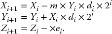
The digit recurrence algorithms mentioned in the previous subsection retire a fixed number of bits at each iteration, using only shift and add operations. Functional iterative algorithms employ multiplication as the fundamental operation and produce at least double the number of correct bits with each iteration (Flynn 1970; Ito et al. 1995; Obermann and Flynn 1997; Oklobdzija and Ercegovac 1982). This is an important factor as there may be as many as three multiplications in each iteration. However, with the advantage of at least quadratic convergence, a 53-bit quotient can be achieved in six iterations, as illustrated in Figure 3.11.
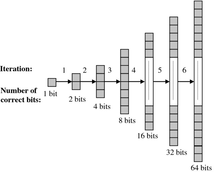
Figure 3.11 Quadratic convergence
3.6 Square Root
Methods for performing the square root operation are similar to those for performing division. They fall broadly into the two categories, digit recurrence methods and methods based on convergence techniques. This section gives a brief overview of each.
3.6.1 Digit Recurrence Square Root
Digit recurrence methods can be based on either restoring or non-restoring techniques, both of which operate msd first. The algorithm is subtractive, and after each iteration the resulting bit is set to 0 if a negative value is found, and then the original remainder is ’restored’ as the new remainder. If the digit is positive, a 1 is set and the new remainder is used. The “non-restoring” algorithm allows the negative value to persist and then performs a compensation addition operation in the next iteration. The overall process of the square root and division algorithms is very similar, and, as such, there have been a number of implementations of systolic arrays designed to perform both arithmetic functions (Ercegovac and Lang 1991; Heron and Woods 1999).
The performance of the algorithms mentioned has been limited due to the dependence of the iterations and the propagated carries along each row. The full values need to be calculated at each stage to enable a correct comparison and decision to be made. The SRT algorithm is a class of non-restoring digit-by-digit algorithms in which the digit can assume both positive and negative non-zero values. It requires the use of a redundant number scheme (Avizienis 1961), thereby allowing digits to take the values 0, − 1 or 1. The most important feature of the SRT method is that the algorithm allows each iteration to be performed without full-precision comparisons at each iteration, thus giving higher performance.
Consider a value R for which the algorithm is trying to find the square root, and Si the partial square root obtained after i iterations. The scaled remainder, Zi, at the ith step is
where 1/4 ⩽ R < 1 and hence 1/2 ⩽ S < 1. From this, a recurrence relation based on previous remainder calculations can be derived as (McQuillan et al. 1993)
where si is the root digit for iteration i − 1. Typically, the initial value for Z0 will be set to R, while the initial estimate of the square root, S1, is set to 0.5 (due to the initial boundaries placed on R).
There exist higher-radix square root algorithms (Ciminiera and Montuschi 1990; Cortadella and Lang 1994; Lang and Montuschi 1992). However, for most algorithms with a radix greater than 2, there is a need to provide an initial estimate for the square root from a LUT. This relates to the following subsection.
3.6.2 Square Root by Functional Iteration
As with the convergence division in Section 3.6.1, the square root calculation can be performed using functional iteration. It can be additive or multiplicative. If additive, then each iteration is based on addition and will retire the same number of bits with each iteration. In other words, they converge linearly to the solution. One example is the CORDIC implementation for performing the Givens rotations for matrix triangularization (Hamill et al. 2000). Multiplicative algorithms offer an interesting alternative as they double the precision of the result with each iteration, that is, they converge quadratically to the result. However, they have the disadvantage of increased computational complexity due to the multiplications within each iterative step.
Similarly to the approaches used in division methods, the square root can be estimated using Newton–Raphson or series convergence algorithms. For the Newton–Raphson method, an iterative algorithm can be found by using
and choosing f(x) that has a root at the solution. One possible choice is f(x) = x2 − b which leads to the following iterative algorithm:
This has the disadvantage of requiring division. An alternative method would be to aim to drive the algorithm toward calculating the reciprocal of the square root, 1/x2. For this, f(x) = 1/x2 − b is used, which leads to the following iterative algorithm:
Once solved, the square root can then be found by multiplying the result by the original value, X, that is, ![]() .
.
Another method for implementing the square root function is to use series convergence, i.e. Goldschmidt’s algorithm (Soderquist and Leeser 1995), which produces equations similar to those for division (Even et al. 2003). The aim of this algorithm is to compute successive iterations to drive one value to 1 while driving the other value to the desired result. To calculate the square root of a value a, for each iteration:
where we let x0 = y0 = a. Then by letting
x → 1 and consequently ![]() . In other words, with each iteration x is driven closer to 1 while y is driven closer to
. In other words, with each iteration x is driven closer to 1 while y is driven closer to ![]() . As with the other convergence examples, the algorithm benefits from using an initial estimate of
. As with the other convergence examples, the algorithm benefits from using an initial estimate of ![]() to pre-scale the initial values of x0 and y0.
to pre-scale the initial values of x0 and y0.
In all of the examples given for both the division and square root convergence algorithms, vast improvements in performance can be obtained by using a LUT to provide an initial estimate to the desired solution. This is covered in the following subsection.
3.6.3 Initial Approximation Techniques
The number of iterations for convergence algorithms can be vastly reduced by providing an initial approximation to the result read from a LUT. For example, the simplest way of forming the approximation R0 to the reciprocal of the divisor D is to read an approximation to 1/D directly from a LUT. The first m bits of the n-bit input value D are used to address the table entry of p bits holding an approximation to the reciprocal. The value held by the table is determined by considering the maximum and minimum errors caused by truncating D from n to m bits.
The time to access a LUT is relatively small so it provides a quick evaluation of the first number of bits to a solution. However, as the size of the input value addressing the LUT increases, the size of the table grows exponentially. For a table addressed by m bits and outputting p bits, the table size will have 2m entries of width p bits. Therefore, the size of the LUT soon becomes very large and will have slower access times.
A combination of p and m can be chosen to achieve the required accuracy for the approximation, with the smallest possible table. By denoting the number of bits by which p is larger than m as the number of guard bits g, the total error Etotal (Sarma and Matula 1993) may be expressed as
Table 3.8 shows the precision of approximations for example values of g and m. These results are useful in determining whether adding a few guard bits might provide sufficient additional accuracy in place of the more costly step in increasing m to m + 1 which more than doubles the table size.
Table 3.8 Precision of approximations for example values of g and m
| Address bits | Guard bits g | Output bits | Precision |
| m | 0 | m | m + 0.415 bits |
| m | 1 | m + 1 | m + 0.678 bits |
| m | 2 | m + 2 | m + 0.830 bits |
| m | 3 | m + 3 | m + 0.912 bits |
Another simple approximation technique is known as read-only memory (ROM) interpolation. Rather than just truncating the value held in memory after the mth bit, the first unseen bit (m + 1) is set to 1, and all bits less significant than it are set to 0 (Fowler and Smith 1989). This has the effect of averaging the error. The resulting approximation is then rounded back to the lsb of the table entry by adding a 1 to the bit location just past the output width of the table. The advantage with this technique is its simplicity. However, it would not be practical for large initial approximations as there is no attempt to reduce the table size.
There are techniques for table compression, such as bipartite tables, which use two or more LUTs and then add the output values to determine the approximation (Schulte et al. 1997). To approximate a reciprocal function using bipartite tables, the input operand is divided into three parts as shown in Figure 3.12.
Figure 3.12 Block diagram for bipartite approximation methods
The n0 + n1 bits provide the address for the first LUT, giving the coefficient a0 of length p0 bits. The sections d0 and d2, equating to n0 + n2 bits, provide addresses for the second LUT, giving the second coefficient a1 of length p1 bits. The outputs from the tables are added together to approximate the reciprocal, R0, using a two-term Taylor series expansion. The objective is to use the first n0 + n1 msbs to provide the lookup for the first table which holds coefficients based on the values given added with the mid-value of the range of values for d2. The calculation of the second coefficient is based on the value from sections d0 and d2 summed with the mid-value of the range of values for d1. This technique forms a method of averaging so that the errors caused by truncation are reduced. The coefficients for the reciprocal approximation take the form
where δ1 and δ2 are constants exactly halfway between the minimum and maximum values for d1 and d2, respectively.
The benefit is that the two small LUTs will have less area than the one large LUT for the same accuracy, even when the size of the addition is considered. Techniques to simplify the bipartite approximation method also exist. One method (Sarma and Matula 1995) eliminates the addition by using each of the two LUTs to store the positive and negative portions of a redundant binary reciprocal value. These are “fused” with slight recoding to round off a couple of low-order bits to obtain the required precision of the least significant bit. With a little extra logic, this recoding can convert the redundant binary values into Booth encoded operands suitable for input into a Booth encoded multiplier.
3.7 Fixed-Point versus Floating-Point
If the natural assumption is that the “most accurate is always best,” then there appears to be no choice in determining the number representation, as floating-point will be chosen. Historically, though, the advantage of FPGAs was in highly efficient implementation of fixed-point arithmetic as some of the techniques given in Chapter 7 will demonstrate. However, the situation is changing as FPGA vendors start to make architectural changes which make implementation of floating-point much more attractive, as will be seen in Chapter 5.
The decision is usually made based on the actual application requirements. For example, many applications vary in terms of the data word sizes and the resulting accuracy. Applications can require different input wordlengths, as illustrated in Table 3.9, and can vary in terms of their sensitivity to errors created as a result of limited, internal wordlength. Obviously, smaller input wordlengths will have smaller internal accuracy requirements, but the perception of the application will also play a major part in determining the internal wordlength requirements. The eye is tolerant of wordlength limitations in images, particularly if they appear as distortion at high frequencies, whereas the ear is particularly intolerant to distortion and noise at any frequency, but specifically high frequency. Therefore cruder truncation may be possible with some image processing applications, but less so in audio applications.
Table 3.9 Typical wordlengths
| Application | Word sizes (bits) |
| Control systems | 4–10 |
| Speech | 8–13 |
| Audio | 16–24 |
| Video | 8–10 |
Table 3.10 gives an estimation of the dynamic range capabilities of some fixed-point representations. It is clear that, depending on the internal computations being performed, many DSP applications can give an acceptable signal-to-noise ratio (SNR) with limited wordlengths, say 12–16 bits. Given the performance gain of fixed-point over floating-point in FPGAs, fixed-point realizations have dominated, but the choice will also depend on application input and output wordlengths, required SNR, internal computational complexity and the nature of computation being performed, i.e. whether specialist operations such as matrix inversions or iterative computations are required.
Table 3.10 Fixed wordlength dynamic range
| Wordlength (bits) | Wordlength range | Dynamic range dB |
| 8 | − 127 to + 127 | 20log 28 ≈ 48 |
| 16 | − 32768 to + 32767 | 20log 216 ≈ 96 |
| 24 | − 8388608 to + 8388607 | 20log 224 ≈ 145 |
A considerable body of work has been dedicated to reducing the number precision to best match the performance requirements. Constantinides et al. (2004) look to derive accurate bit approximations for internal wordlengths by considering the impact on design quality. A floating-point design flow is presented in Fang et al. (2002) which takes an algorithmic input and generates floating-point hardware by performing bit width optimization, with a cost function related to hardware, but also to power consumption. This activity is usually performed manually by the designer, using suitable fixed-point libraries in tools such as MATLAB® or LabVIEW, as suggested earlier.
3.7.1 Floating-Point on FPGA
Up until recently, FPGAs were viewed as being poor for floating-point realization. However, the adoption of a dedicated DSP device in each of the main vendors’ FPGA families means that floating-point implementation has become much more attractive, particularly if a latency can be tolerated. Table 3.11 gives area and clock speed figures for floating core implementation on a Xilinx Virtex-7 device. The speed is determined by the capabilities of the DSP48E1 core and pipelining within the programmable logic.
Table 3.11 Xilinx floating-point LogiCORE v7.0 on Virtex-7
| Function | DSP48 | LUT | Flip-flops | Speed (MHz) |
| Single range multiplier | 2 | 96 | 166 | 462 |
| Double range multiplier | 10 | 237 | 503 | 454 |
| Single range accumulator | 7 | 3183 | 3111 | 360 |
| Double range accumulator | 45 | 31738 | 24372 | 321 |
| Single range divider | 0 | 801 | 1354 | 579 |
| Double range divider | 0 | 3280 | 1982 | 116.5 |
The area comparison for floating-point is additionally complicated as the relationship between multiplier and adder area is now changed. In fixed-point, multipliers are generally viewed to be N times bigger than adders, where N is the wordlength. However, in floating-point, the area of floating-point adders is not only comparable to that of floating-point multipliers but, in the case of double point precision, is much larger than that of a multiplier and indeed slower. This corrupts the assumption, at the DSP algorithmic stage, that reducing the number of multiplications in favor of additions is a good optimization.
Calculations in Hemsoth (2012) suggest that the current generation of Xilinx’s Virtex-7 FPGAs is about 4.2 times faster than a 16-core microprocessor. This figure is up from a factor of 2.9× as reported in an earlier study in 2010 and suggests that the inclusion of dedicated circuitry is improving the floating-point performance. However, these figures are based on estimated performance and not on a specific application implementation. They indicate 1.33 tera floating-point operations per second (TFLOPS) of single-precision floating-point performance on one device (Vanevenhoven 2011).
Altera have gone one stage further by introducing dedicated hardened circuitry into the DSP blocks to natively support IEEE 754 single-precision floating-point arithmetic (Parker 2012). As all of the complexities of IEEE 754 floating-point are built within the hard logic of the DSP blocks, no programmable logic is consumed and similar clock rates to those for fixed-point designs are achieved. With thousands of floating-point operators built into these hardened DSP blocks, the Altera Arria® 10 FPGAs are rated from 140 giga floating-point operations per second (GFLOPS) to 1.5 TFLOPS across the 20 nm family. This will also be employed in the higher-performance Altera 14 nm Stratix® 10 FPGA family, giving a performance range right up to 10 TFLOPS!
Moreover, the switch to heterogeneous SoC FPGA devices also offers floating-point arithmetic in the form of dedicated ARM processors. As will be seen in subsequent chapters, this presents new mapping possibilities for FPGAs as it is now possible to map the floating-point requirements into the dedicated programmable ARM resources and then employ the fixed-point capabilities of dedicated SoC.
3.8 Conclusions
This chapter has given a brief grounding in computer arithmetic basics and given some idea of the hardware needed to implement basic computer arithmetic functions and some more complex functions such as division and square root. Whilst the chapter outlines the key performance decisions, it is clear that the availability of dedicated adder and multiplier circuitry has made redundant a lot of FPGA-based research into new types of adder/multiplier circuits using different forms of arithmetic.
The chapter has also covered some critical aspects of arithmetic representations and the implications that choice of either fixed- or floating-point arithmetic can have in terms of hardware implementation, particularly given the current FPGA support for floating-point. It clearly demonstrates that FPGA technology is currently very appropriate for fixed-point implementation, but increasingly starting to include floating-point arithmetic capability.
Bibliography
- Albicocco P, Cardarilli GC, Nannarelli A, Re M 2014 Twenty years of research on RNS for DSP: Lessons learned and future perspectives. In Proc. Int. Symp. on Integrated Circuits, pp. 436–439, doi: 10.1109/ISICIR.2014.7029575.
- Andrews M 1986 A systolic SBNR adaptive signal processor. IEEE Trans. on Circuits and Systems, 33(2), 230–238.
- Avizienis A 1961 Signed-digit number representations for fast parallel arithmetic. IRE Trans. on Electronic Computers, 10, 389–400.
- Chandrakasan A, Brodersen R 1996 Low Power Digital Design. Kluwer, Dordrecht.
- Ciminiera L, Montuschi P 1990 Higher radix square rooting. IEEE Trans. on Computing, 39(10), 1220–1231.
- Collange S, Detrey J, de Dinechin F 2006 Floating point or Ins: choosing the right arithmetic on an application basis. In Proc. EUROMICRO Conf. on Digital System Design, pp. 197–203.
- Constantinides G, Cheung PYK, Luk W 2004 Synthesis and Optimization of DSP Algorithms. Kluwer, Dordrecht.
- Cortadella J, Lang T 1994 High-radix division and square-root with speculation. IEEE Trans. on Computers, 43(8), 919–931.
- Detrey J, de Dinechin FAV 2003 HDL library of LNS operators. In Proc. 37th IEEE Asilomar Conf. on Signals, Systems and Computers, 2, pp. 2227–2231.
- Ercegovac MD, Lang T 1990 Redundant and on-line cordic: Application to matrix triangularization. IEEE Trans. on Computers, 39(6), 725–740.
- Ercegovac MD, Lang T 1991 Module to perform multiplication, division, and square root in systolic arrays for matrix computations. J. of Parallel Distributed Computing, 11(3), 212–221.
- Even G, Seidel PM, Ferguson W 2003 A parametric error analysis of Goldschmidt’s division algorithm. In Proc. IEEE Symp. on Computer Arithmetic, pp. 165–171.
- Fang F, Chen T, Rutenbar RA 2002 Floating-point bit-width optimisation for low-power signal processing applications. In Proc. of IEEE Int. Conf. on Acoustics, Speech and Signal Processing, 3, pp. 3208–3211.
- Flynn M 1970 On division by functional iteration. IEEE Trans. on Computers, 19(8), 702–706.
- Fowler DL, Smith JE 1989 High speed implementation of division by reciprocal approximation. In Proc. IEEE Symp. on Computer Arithmetic, pp. 60–67.
- Hamill R, McCanny J, Walke R 2000 Online CORDIC algorithm and VLSI architecture for implementing QR-array processors. IEEE Trans. on Signal Processing, 48(2), 592–598.
- Hauck S, Hosler MM, Fry TW 2000 High-performance carry chains for FPGAs. IEEE Trans. on VLSI Systems, 8(2), 138–147.
- Haselman M, Beauchamp M, Wood A, Hauck S, Underwood K, Hemmert KS 2005 A comparison of floating point and logarithmic number systems for FPGAs. In Proc. IEEE Symp. on FPGA-based Custom Computing Machines, pp. 181–190.
- Hemsoth N 2012. Latest FPGAs show big gains in floating point performance. HPCWire, April 16.
- Heron JP, Woods RF 1999 Accelerating run-time reconfiguration on FCCMs. Proc. IEEE Symp. on FPGA-based Custom Computing Machines, pp. 260–261.
- Hoe DHK, Martinez C, Vundavalli SJ 2011 Design and characterization of parallel prefix adders using FPGAs. In Proc. IEEE Southeastern Symp. on Syst. Theory, pp. 168–172.
- Ito M, Takagi N, Yajima S 1995 Efficient initial approximation and fast converging methods for division and square root. In Proc. IEEE Symp. on Computer Arithmetic, pp. 2–9.
- Knowles S, Woods RF, McWhirter JG, McCanny JV 1989 Bit-level systolic architectures for high performance IIR filtering. J. of VLSI Signal Processing, 1(1), 9–24.
- Koren I 2002 Computer Arithmetic Algoritmns, 2nd edition A.K. Peters, Natick, MA.
- Lang T, Montuschi P 1992 Higher radix square root with prescaling. IEEE Trans. on Computers, 41(8), 996–1009.
- Ma J, Deprettere EF, Parhi K I997 Pipelined cordic based QRD-RLS adaptive filtering using matrix lookahead. In Proc. IEEE Int. Workshop on Signal Processing Systems, pp. 131–140.
- McQuillan SE, McCanny J, Hamill R 1993 New algorithms and VLSI architectures for SRT division and square root. In Proc. IEEE Symp. on Computer Arithmetic, pp. 80–86.
- Meyer-Baese U, García A, Taylor F. 2001. Implementation of a communications channelizer using FPGAs and RNS arithmetic. J. VLSI Signal Processing Systems, 28(1–2), 115–128.
- Muller JM 2005 Elementary Functions, Algorithms and Implementation. Birkhäuser, Boston.
- Obermann SF, Flynn MJ 1997 Division algorithms and implementations. IEEE Trans. on Computers, 46(8), 833–854.
- Oklobdzija V, Ercegovac M 1982 On division by functional iteration. IEEE Trans. on Computers, 31(1), 70–75.
- Omondi AR 1994 Computer Arithmetic Systems. Prentice Hall, New York.
- Parker M 2012 The industry’s first floating-point FPGA. Altera Backgrounder. http://bit.ly/2eF01WT
- Robertson, J 1958 A new class of division methods. IRE Trans. on Electronic Computing, 7, 218–222.
- Sarma DD, Matula DW 1993 Measuring the accuracy of ROM reciprocal tables. In Proc. IEEE Symp. on Computer Arithmetic, pp. 95–102.
- Sarma DD, Matula DW 1995 Faithful bipartite ROM reciprocal tables. In Proc. IEEE Symp. on Computer Arithmetic, pp. 17–28.
- Schulte MJ, Stine IE, Wires KE 1997 High-speed reciprocal approximations. In Proc. IEEE Asilomar Conference on Signals, Systems and Computers, pp. 1183–1187.
- Sklansky J 1960 Conditional sum addition logic. IRE Trans. on Electronic Computers, 9(6), 226–231.
- Soderquist P, Leeser M 1995 An area/performance comparison of subtractive and multiplicative divide/square root implementations. In Proc. IEEE Symp. on Computer Arithmetic, pp. 132–139.
- Soderstrand MA, Jenkins WK, Jullien GA, Taylor FJ 1986 Residue Number Systems Arithmetic: Modern Applications in Digital Signal Processing. IEEE Press, Piscataway, NJ.
- Takagi N, Asada T, Yajima S 1991 Redundant CORDIC methods with a constant scale factor for sine and cosine computation. IEEE Trans. on Computers, 40(9), 989–995.
- Tichy M, Schier J, Gregg D 2006 Efficient floating-point implementation of high-order (N)LMS adaptive filters in FPGA. In Bertels K, Cardoso JMP, Vassiliadis (eds) Reconfigurable Computing: Architectures and Applications, Lecture Notes in Computer Science 3985, pp. 311–316. Springer, Berlin.
- Tocher K 1958 Techniques of multiplication and division for automatic binary computers. Quart. J. of Mech. and Applied Mathematics. 1l(3), 364–384.
- Vanevenhoven T 2011, High-level implementation of bit- and cycle-accurate floating-point DSP algorithms with Xilinx FPGAs. Xilinx White Paper: 7 Series FPGAs WP409 (v1.0).
- Voider JE 1959 The CORDIC trigonometric computing technique. IRE Trans. on Electronic Computers, 8(3), 330–334.
- Wallace CS 1964 A suggestion for a fast multiplier. IEEE Trans. on Electronic Computers, 13(1), 14–17.
- Walther JS 1971 A unified algorithm for elementary functions. In Proc. Spring Joint Computing Conference, pp. 379–385.
- Xing S, Yu WWh 1998. FPGA adders: performance evaluation and optimal design. IEEE Design and Test of Computers, 15(1), 24–29.
- Yeh W-C, Jen C-W 2000 High-speed Booth encoded parallel multiplier design, IEEE Trans. on Computers, 49(7), 692–701.