1
Introduction to Field Programmable Gate Arrays
1.1 Introduction
Electronics continues to make an impact in the twenty-first century and has given birth to the computer industry, mobile telephony and personal digital entertainment and services industries, to name but a few. These markets have been driven by developments in silicon technology as described by Moore’s law (Moore 1965), which is represented pictorially in Figure 1.1. This has seen the number of transistors double every 18 months. Moreover, not only has the number of transistors doubled at this rate, but also the costs have decreased, thereby reducing the cost per transistor at every technology advance.
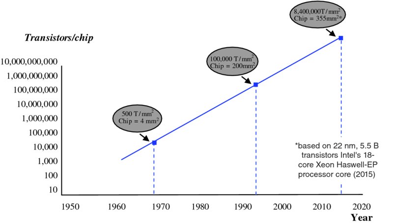
Figure 1.1 Moore’s law
In the 1970s and 1980s, electronic systems were created by aggregating standard components such as microprocessors and memory chips with digital logic components, e.g. dedicated integrated circuits along with dedicated input/output (I/O) components on printed circuit boards (PCBs). As levels of integration grew, manufacturing working PCBs became more complex, largely due to greater component complexity in terms of the increase in the number of transistors and I/O pins. In addition, the development of multi-layer boards with as many as 20 separate layers increased the design complexity. Thus, the probability of incorrectly connecting components grew, particularly as the possibility of successfully designing and testing a working system before production was coming under greater and greater time pressures.
The problem became more challenging as system descriptions evolved during product development. Pressure to create systems to meet evolving standards, or that could change after board construction due to system alterations or changes in the design specification, meant that the concept of having a “fully specified” design, in terms of physical system construction and development on processor software code, was becoming increasingly challenging. Whilst the use of programmable processors such as microcontrollers and microprocessors gave some freedom to the designer to make alterations in order to correct or modify the system after production, this was limited. Changes to the interconnections of the components on the PCB were restricted to I/O connectivity of the processors themselves. Thus the attraction of using programmability interconnection or “glue logic” offered considerable potential, and so the concept of field programmable logic (FPL), specifically field programmable gate array (FPGA) technology, was born.
From this unassuming start, though, FPGAs have grown into a powerful technology for implementing digital signal processing (DSP) systems. This emergence is due to the integration of increasingly complex computational units into the fabric along with increasing complexity and number of levels in memory. Coupled with a high level of programmable routing, this provides an impressive heterogeneous platform for improved levels of computing. For the first time ever, we have seen evolutions in heterogeneous FPGA-based platforms from Microsoft, Intel and IBM. FPGA technology has had an increasing impact on the creation of DSP systems. Many FPGA-based solutions exist for wireless base station designs, image processing and radar systems; these are, of course, the major focus of this text.
Microsoft has developed acceleration of the web search engine Bing using FPGAs and shows improved ranking throughput in a production search infrastructure. IBM and Xilinx have worked closely together to show that they can accelerate the reading of data from web servers into databases by applying an accelerated Memcache2; this is a general-purpose distributed memory caching system used to speed up dynamic database-driven searches (Blott and Vissers 2014). Intel have developed a multicore die with Altera FPGAs, and their recent purchase of the company (Clark 2015) clearly indicates the emergence of FPGAs as a core component in heterogeneous computing with a clear target for data centers.
1.2 Field Programmable Gate Arrays
The FPGA concept emerged in 1985 with the XC2064™ FPGA family from Xilinx. At the same time, a company called Altera was also developing a programmable device, later to become the EP1200, which was the first high-density programmable logic device (PLD). Altera’s technology was manufactured using 3-μm complementary metal oxide semiconductor (CMOS) electrically programmable read-only memory (EPROM) technology and required ultraviolet light to erase the programming, whereas Xilinx’s technology was based on conventional static random access memory (SRAM) technology and required an EPROM to store the programming.
The co-founder of Xilinx, Ross Freeman, argued that with continuously improving silicon technology, transistors were going to become cheaper and cheaper and could be used to offer programmability. This approach allowed system design errors which had only been recognized at a late stage of development to be corrected. By using an FPGA to connect the system components, the interconnectivity of the components could be changed as required by simply reprogramming them. Whilst this approach introduced additional delays due to the programmable interconnect, it avoided a costly and time-consuming PCB redesign and considerably reduced the design risks.
At this stage, the FPGA market was populated by a number of vendors, including Xilinx, Altera, Actel, Lattice, Crosspoint, Prizm, Plessey, Toshiba, Motorola, Algotronix and IBM. However, the costs of developing technologies not based on conventional integrated circuit design processes and the need for programming tools saw the demise of many of these vendors and a reduction in the number of FPGA families. SRAM technology has now emerged as the dominant technology largely due to cost, as it does not require a specialist technology. The market is now dominated by Xilinx and Altera, and, more importantly, the FPGA has grown from a simple glue logic component to a complete system on programmable chip (SoPC) comprising on-board physical processors, soft processors, dedicated DSP hardware, memory and high-speed I/O.
The FPGA evolution was neatly described by Steve Trimberger in his FPL2007 plenary talk (see the summary in Table 1.1). The evolution of the FPGA can be divided into three eras. The age of invention was when FPGAs started to emerge and were being used as system components typically to provide programmable interconnect giving protection to design evolutions and variations. At this stage, design tools were primitive, but designers were quite happy to extract the best performance by dealing with lookup tables (LUTs) or single transistors.
Table 1.1 Three ages of FPGAs
| Period | Age | Comments |
| 1984–1991 | Invention | Technology is limited, FPGAs are much smaller than the application problem size. Design automation is secondary, architecture efficiency is key |
| 1992–1999 | Expansion | FPGA size approaches the problem size. Ease of design becomes critical |
| 2000–present | Accumulation | FPGAs are larger than the typical problem size. Logic capacity limited by I/O bandwidth |
As highlighted above, there was a rationalization of the technologies in the early 1990s, referred to by Trimberger as the great architectural shakedown. The age of expansion was when the FPGA started to approach the problem size and thus design complexity was key. This meant that it was no longer sufficient for FPGA vendors to just produce place and route tools and it became critical that hardware description languages (HDLs) and associated synthesis tools were created. The final evolution period was the period of accumulation when FPGAs started to incorporate processors and high-speed interconnection. Of course, this is very relevant now and is described in more detail in Chapter 5 where the recent FPGA offerings are reviewed.
This has meant that the FPGA market has grown from nothing in just over 20 years to become a key player in the IC industry, worth some $3.9 billion in 2014 and expected to be worth around $7.3 billion in 2022 (MarketsandMarkets 2016). It has been driven by the growth in the automotive sector, mobile devices in the consumer electronics sector and the number of data centers.
1.2.1 Rise of Heterogeneous Computing Platforms
Whilst Moore’s law is presented here as being the cornerstone for driving FPGA evolution and indeed electronics, it also has been the driving force for computing. However, all is not well with computing’s reliance on silicon technology. Whilst the number of transistors continues to double, the scaling of clock speed has not continued at the same rate. This is due to the increase in power consumption, particularly the increase in static power. The issue of the heat dissipation capability of packaging means that computing platform providers such as Intel have limited their processor power to 30 W. This resulted in an adjustment in the prediction for clock rates between 2005 and 2011 (as illustrated in Figure 1.2) as clock rate is a key contributor to power consumption (ITRS 2005).
Figure 1.2 Change in ITRS scaling prediction for clock frequencies
In 2005, the International Technology Roadmap for Semiconductors (ITRS) predicted that a 100 GHz clock would be achieved in 2020, but this estimation had to be revised first in 2007 and then again in 2011. This has been seen in the current technology where a clock rate of some 30 GHz was expected in 2015 based on the original forecast, but we see that speeds have been restricted to 3–4 GHz. This has meant that the performance per gigahertz has effectively stalled since 2005 and has generated the interest by major computing companies in exploring different architectures that employ FPGA technology (Putnam et al. 2014; Blott and Vissers 2014).
1.2.2 Programmability and DSP
On many occasions, the growth indicated by Moore’s law has led people to argue that transistors are essentially free and therefore can be exploited, as in the case of programmable hardware, to provide additional flexibility. This could be backed up by the observation that the cost of a transistor has dropped from one-tenth of a cent in the 1980s to one-thousandth of a cent in the 2000s. Thus we have seen the introduction of hardware programmability into electronics in the form of FPGAs.
In order to make a single transistor programmable in an SRAM technology, the programmability is controlled by storing a “1” or a “0” on the gate of the transistor, thereby making it conduct or not. This value is then stored in an SRAM cell which, if it requires six transistors, will will mean that we need seven transistors to achieve one programmable equivalent in FPGA. The reality is that in an overall FPGA implementation, the penalty is nowhere as harsh as this, but it has to be taken into consideration in terms of ultimate system cost.
It is the ability to program the FPGA hardware after fabrication that is the main appeal of the technology; this provides a new level of reassurance in an increasingly competitive market where “right first time” system construction is becoming more difficult to achieve. It would appear that that assessment was vindicated in the late 1990s and early 2000s: when there was a major market downturn, the FPGA market remained fairly constant when other microelectronic technologies were suffering. Of course, the importance of programmability has already been demonstrated by the microprocessor, but this represented a new change in how programmability was performed.
The argument developed in the previous section presents a clear advantage of FPGA technology in overcoming PCB design errors and manufacturing faults. Whilst this might have been true in the early days of FPGA technology, evolution in silicon technology has moved the FPGA from being a programmable interconnection technology to making it into a system component. If the microprocessor or microcontroller was viewed as programmable system component, the current FPGA devices must also be viewed in this vein, giving us a different perspective on system implementation.
In electronic system design, the main attraction of the microprocessor is that it considerably lessens the risk of system development. As the hardware is fixed, all of the design effort can be concentrated on developing the code. This situation has been complemented by the development of efficient software compilers which have largely removed the need for the designer to create assembly language; to some extent, this can even absolve the designer from having a detailed knowledge of the microprocessor architecture (although many practitioners would argue that this is essential to produce good code). This concept has grown in popularity, and embedded microprocessor courses are now essential parts of any electrical/electronic or computer engineering degree course.
A lot of this process has been down to the software developer’s ability to exploit an underlying processor architecture, the von Neumann architecture. However, this advantage has also been the limiting factor in its application to the topic of this text, namely DSP. In the von Neumann architecture, operations are processed sequentially, which allows relatively straightforward interpretation of the hardware for programming purposes; however, this severely limits the performance in DSP applications which exhibit high levels of parallelism and have operations that are highly data-independent. This cries out for parallel realization, and whilst DSP microprocessors go some way toward addressing this situation by providing concurrency in the form of parallel hardware and software “pipelining,” there is still the concept of one architecture suiting all sizes of the DSP problem.
This limitation is overcome in FPGAs as they allow what can be considered to be a second level of programmability, namely programming of the underlying processor architecture. By creating an architecture that best meets the algorithmic requirements, high levels of performance in terms of area, speed and power can be achieved. This concept is not new as the idea of deriving a system architecture to suit algorithmic requirements has been the cornerstone of application-specific integrated circuit (ASIC) implementations. In high volumes, ASIC implementations have resulted in the most cost-effective, fastest and lowest-energy solutions. However, increasing mask costs and the impact of “right first time” system realization have made the FPGA a much more attractive alternative.
In this sense, FPGAs capture the performance aspects offered by ASIC implementation, but with the advantage of programmability usually associated with programmable processors. Thus, FPGA solutions have emerged which currently offer several hundreds of giga operations per second (GOPS) on a single FPGA for some DSP applications, which is at least an order of magnitude better performance than microprocessors.
1.3 Influence of Programmability
In many texts, Moore’s law is used to highlight the evolution of silicon technology, but another interesting viewpoint particularly relevant for FPGA technology is Makimoto’s wave, which was first published in the January 1991 edition of Electronics Weekly. It is based on an observation by Tsugio Makimoto who noted that technology has shifted between standardization and customization. In the 1960s, 7400 TTL series logic chips were used to create applications; and then in the early 1970s, the custom large-scale integration era emerged where chips were created (or customized) for specific applications such as the calculator. The chips were now increasing in their levels of integration and so the term “medium-scale integration” (MSI) was born. The evolution of the microprocessor in the 1970s saw the swing back towards standardization where one “standard” chip was used for a wide range of applications.
The 1980s then saw the birth of ASICs where designers could overcome the fact that the sequential microprocessor posed severe limitations in DSP applications where higher levels of computations were needed. The DSP processor also emerged, such as the TMS32010, which differed from conventional processors as they were based on the Harvard architecture which had separate program and data memories and separate buses. Even with DSP processors, ASICs offered considerable potential in terms of processing power and, more importantly, power consumption. The development of the FPGA from a “glue component” that allowed other components to be connected together to form a system to become a component or even a system itself led to its increased popularity.
The concept of coupling microprocessors with FPGAs in heterogeneous platforms was very attractive as this represented a completely programmable platform with microprocessors to implement the control-dominated aspects of DSP systems and FPGAs to implement the data-dominated aspects. This concept formed the basis of FPGA-based custom computing machines (FCCMs) which formed the basis for “configurable” or reconfigurable computing (Villasenor and Mangione-Smith 1997). In these systems, users could not only implement computational complex algorithms in hardware, but also use the programmability aspect of the hardware to change the system functionality, allowing the development of “virtual hardware” where hardware could ‘virtually” implement systems that are an order of magnitude larger (Brebner 1997).
We would argue that there have been two programmability eras. The first occurred with the emergence of the microprocessor in the 1970s, where engineers could develop programmable solutions based on this fixed hardware. The major challenge at this time was the software environments; developers worked with assembly language, and even when compilers and assemblers emerged for C, best performance was achieved by hand-coding. Libraries started to appear which provided basic common I/O functions, thereby allowing designers to concentrate on the application. These functions are now readily available as core components in commercial compilers and assemblers. The need for high-level languages grew, and now most programming is carried out in high-level programming languages such as C and Java, with an increased use of even higher-level environments such as the unified modeling language (UML).
The second era of programmability was ushered in by FPGAs. Makimoto indicates that field programmability is standardized in manufacture and customized in application. This can be considered to have offered hardware programmability if you think in terms of the first wave as the programmability in the software domain where the hardware remains fixed. This is a key challenge as most computer programming tools work on the fixed hardware platform principle, allowing optimizations to be created as there is clear direction on how to improve performance from an algorithmic representation. With FPGAs, the user is given full freedom to define the architecture which best suits the application. However, this presents a problem in that each solution must be handcrafted and every hardware designer knows the issues in designing and verifying hardware designs!
Some of the trends in the two eras have similarities. In the early days, schematic capture was used to design early circuits, which was synonymous with assembly-level programming. Hardware description languages such as VHSIC Hardware Description Language (VHDL) and Verilog then started to emerge that could used to produce a higher level of abstraction, with the current aim to have C-based tools such as SystemC and Catapult® from Mentor Graphics as a single software-based programming environment (Very High Speed Integrated Circuit (VHSIC) was a US Department of Defense funded program in the late 1970s and early 1980s with the aim of producing the next generation of integrated circuits). Initially, as with software programming languages, there was mistrust in the quality of the resulting code produced by these approaches.
With the establishment of improved cost-effectiveness, synthesis tools are equivalent to the evolution of efficient software compilers for high-level programming languages, and the evolution of library functions allowed a high degree of confidence to be subsequently established; the use of HDLs is now commonplace for FPGA implementation. Indeed, the emergence of intellectual property (IP) cores mirrored the evolution of libraries such as I/O programming functions for software flows; they allowed common functions to be reused as developers trusted the quality of the resulting implementation produced by such libraries, particularly as pressures to produce more code within the same time-span grew. The early IP cores emerged from basic function libraries into complex signal processing and communications functions such as those available from the FPGA vendors and the various web-based IP repositories.
1.4 Challenges of FPGAs
In the early days, FPGAs were seen as glue logic chips used to plug components together to form complex systems. FPGAs then increasingly came to be seen as complete systems in themselves, as illustrated in Table 1.1. In addition to technology evolution, a number of other considerations accelerated this. For example, the emergence of the FPGA as a DSP platform was accelerated by the application of distributed arithmetic (DA) techniques (Goslin 1995; Meyer-Baese 2001). DA allowed efficient FPGA implementations to be realized using the lookup table or LUT-based/adder constructs of FPGA blocks and allowed considerable performance gains to be gleaned for some DSP transforms such as fixed coefficient filtering and transform functions such as the fast Fourier transform (FFT). Whilst these techniques demonstrated that FPGAs could produce highly effective solutions for DSP applications, the idea of squeezing the last aspect of performance out of the FPGA hardware and, more importantly, spending several person-months creating such innovative designs was now becoming unacceptable.
The increase in complexity due to technology evolution meant that there was a growing gap in the scope offered by current FPGA technology and the designer’s ability to develop solutions efficiently using currently available tools. This was similar to the “design productivity gap” (ITRS 1999) identified in the ASIC industry where it was perceived that ASIC design capability was only growing at 25% whereas Moore’s law growth was 60%. The problem is not as severe in FPGA implementation as the designer does not have to deal with sub-micrometer design issues. However, a number of key issues exist:
- Understanding how to map DSP functionality into FPGA. Some of the aspects are relatively basic in this arena, such as multiply-accumulate (MAC) and delays being mapped onto on-board DSP blocks, registers and RAM components, respectively. However, the understanding of floating-point versus fixed-point, wordlength optimization, algorithmic transformation cost functions for FPGA and impact of routing delay are issues that must be considered at a system level and can be much harder to deal with at this level.
- Design languages. Currently hardware description languages such as VHDL and Verilog and their respective synthesis flows are well established. However, users are now looking at FPGAs, with the recent increase in complexity resulting in the integration of both fixed and programmable microprocessor cores as a complete system. Thus, there is increased interest in design representations that more clearly represent system descriptions. Hence there is an increased electronic design automation focus on using C as a design language, but other representations also exist such as those methods based on model of computation (MoC), e.g. synchronous dataflow.
- Development and use of IP cores. With the absence of quick and reliable solutions to the design language and synthesis issues, the IP market in SoC implementation has emerged to fill the gap and allow rapid prototyping of hardware. Soft cores are particularly attractive as design functionality can be captured using HDLs and efficiently translated into the FPGA technology of choice in a highly efficient manner by conventional synthesis tools. In addition, processor cores have been developed which allow dedicated functionality to be added. The attraction of these approaches is that they allow application-specific functionality to be quickly created as the platform is largely fixed.
- Design flow. Most of the design flow capability is based around developing FPGA functionality from some form of higher-level description, mostly for complex functions. The reality now is that FPGA technology is evolving at such a rate that systems comprising FPGAs and processors are starting to emerge as an SoC platform or indeed, FPGAs as a single SoC platform as they have on-board hard and soft processors, high-speed communications and programmable resource, and this can be viewed as a complete system. Conventionally, software flows have been more advanced for processors and even multiple processors as the architecture is fixed. Whilst tools have developed for hardware platforms such as FPGAs, there is a definite need for software for flows for heterogeneous platforms, i.e. those that involve both processors and FPGAs.
These represent the challenges that this book aims to address and provide the main focus for the work that is presented.
Bibliography
- Blott M, Vissers K 2014 Dataflow architectures for 10Gbps line-rate key-value-stores. In Proc. IEEE Hot Chips, Palo Alto, CA.
- Brebner G 1997 The swappable logic unit. In Proc. IEEE Symp. on FCCM, Napa, CA, pp. 77–86.
- Clark D 2015 Intel completes acquisition of Altera. Wall Street J., December 28.
- Goslin G 1995 Using Xilinx FPGAs to design custom digital signal processing devices. In Proc. DSPX, pp. 565–604.
- ITRS 1999 International Technology Roadmap for Semiconductors, Semiconductor Industry Association. Downloadable from http://public.itrs.net (accessed February 16, 2016).
- ITRS 2005 International Technology Roadmap for Semiconductors: Design. available from http://www.itrs.net/Links/2005ITRS/Design2005.pdf (accessed February 16, 2016).
- MarketsandMarkets 2016 FPGA Market, by Architecture (SRAM Based FPGA, Anti-Fuse Based FPGA, and Flash Based FPGA), Configuration (High-End FPGA, Midrange FPGA, and Low-End FPGA), Application, and Geography - Trends & Forecasts to 2022. Report Code: SE 3058, downloadable from marketsandmarkets.com (accessed February 16, 2016).
- Meyer-Baese U 2001 Digital Signal Processing with Field Programmable Gate Arrays Springer, Berlin.
- Moore GE 1965 Cramming more components onto integrated circuits. In Electronics. Available from http://www.cs.utexas.edu/ fussell/courses/cs352h/papers/moore.pdf (accessed February 16, 2016).
- Putnam A, Caulfield AM, Chung ES, Chiou D, Constantinides K, Demme J, Esmaeilzadeh H, Fowers J, Gopal GP, Gray J, Haselman M, Hauck S, Heil S, Hormati A, Kim J-Y, Lanka S, Larus J, Peterson E, Pope S, Smith A, Thong J, Xiao PY, Burger D 2014 A reconfigurable fabric for accelerating large-scale datacenter services. In Proc. IEEE Int. Symp. on Computer Architecture, pp. 13–24.
- Villasenor J, Mangione-Smith WH 1997 Configurable computing. Scientific American, 276(6), 54–59.