6
Detailed FPGA Implementation Techniques
6.1 Introduction
Chapter 4 highlighted the wide range of technologies available for implementing DSP systems and Chapter 5 described the various FPGA offerings. The remaining chapters now describe the issues for implementing complex DSP systems onto FPGA-based heterogeneous platforms and also a single FPGA device! This encompasses considerations such as selection of a suitable model for DSP system implementation, partitioning of DSP complexity into hardware and software, mapping of DSP functions efficiently onto FPGA hardware, development of a suitable memory architecture, and achievement of design targets in terms of throughput, area and energy. However, it is imperative that the reader understands the detailed FPGA implementation of DSP functionality in order that this process is inferred correctly at both the system partitioning and circuit architecture development stages.
A key advantage of FPGAs is that the user can develop highly parallel, pipelined circuitry which can offer very high levels of performance. If these individual circuits can be optimized to exploit specific features of the underlying hardware, then this will offer increased speed or allow more processing functionality, or even both. This comes from efficiently mapping data paths or, in some cases, the controlling circuitry which controls the flow of data, into FPGA hardware. Controllers are usually mapped into finite state machines (FSMs) or implemented as software routines in dedicated processors such as the ARM™ processor in the Xilinx Zynq® or Altera Stratix® 10 devices.
There are a number of areas where circuit-level optimizations may come into play. For example, the user must consider how circuitry maps into LUT-based architectures and schemes for implementing efficient FSMs. A lot of these optimizations are included in synthesis compiler tools so are only briefly reviewed here. Other features may be specific to the data paths and exploit the underlying FPGA hardware features.
At the system partitioning level, for example, it may become clear that the current system under consideration will consume more than the dedicated multiplicative resources available. The designer can then restrict the design space so that the mapping ensures that only the dedicated multiplier resources are used, or other FPGA resources such as LUTs and dedicated adders, to implement the additional multiplicative need. Indeed, if the DSP functions use operators where the coefficients do not change, then it may be possible to build area-efficient fixed-coefficient multipliers. From a circuit architecture perspective, it may be possible to balance the use of the FPGA dedicated DSP blocks against the LUT/fast adder hardware, thus providing a balance between FPGA resource area and throughput rate. For this reason, techniques for efficiently implementing LUT-based structures for single and limited range of coefficients are covered.
Section 6.2 treats the programmable logic elements in the FPGA and highlights how the LUT and dedicated adder circuitry can be used for implementing logic and DSP functionality. Some simple optimizations for mapping into LUTs and efficient implementation of FSMs are covered in Section 6.3. In Section 6.4, the class of fixed-coefficient filters and transforms is described with some discussion on how they can be mapped efficiently into programmable logic. Techniques called distributed arithmetic and reduced coefficient multiplier (RCM) used to implemented fixed or limited-range coefficient functions are then described in Sections 6.5 and 6.6, respectively. Final comments are made in Section 6.7.
6.2 FPGA Functionality
The previous chapter highlighted a number of different FPGA technologies, which to a large extent could be classified as having the following characteristics:
- Programmable elements comprising of a small memory element, typically a LUT, registers(s) and some form of fast addition. The LUT resource varies in size resource from a four-input in the Lattice’s iCE40isp and Microsemi’s RTG4 FPGA, through a six-input in Xilinx’s Zynq® and UltraScale+TM families, to an eight-input LUT in Altera’s Stratix® V and 10 families. Most fast adder circuitry is based around a single-bit adder with the other functionality implemented in the LUT.
- Dedicated DSP resources usually targeted at fixed-point multiply-accumulate functionality, typically 18-bit data input for Xilinx, Microsemi RTG4 and Altera FPGAs and 16-bit for the Lattice iCE40isp. Additional accumulation and subtracter circuitry is available for creating FIR filter and transform circuitry. The wordlengths are such that they are highly suitable for fixed-point implementation for a range of audio, speech, video and radar applications.
- Distributed memory can be used for storage of values or creation of dedicated DSP functionality, in the form of either registers and LUTs in the programmable logic blocks, or 640 b and 20 kB embedded RAM blocks in Altera’s Stratix® family and 36 kB distributed random access memory (disRAM) blocks in the Xilinx families.
It is worth examining these elements in a little more detail with the aim of gauging how they can be used to create efficient DSP functionality by fully considering their range of application.
6.2.1 LUT Functionality
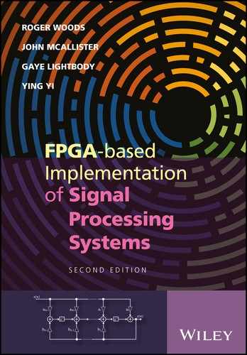
The reason why most FPGA vendors chose the LUT as the logic fundamental building block, is that an n-input LUT can implement any n-input logic function. As shown in Figure 6.1, the use of LUTs places different constraints on the design than the use of logic gates. The diagram shows how the function can be mapped into logic gates, where the number of gates is the design constraint, but this is irrelevant from a LUT implementation perspective, as the underlying criterion is the number of functional inputs.
Figure 6.1 Mapping logic functionality into LUTs
The cost model is therefore more directly related to determining the number of LUTs which is directly impacted by the number of inputs and number of outputs in the design rather than the logic complexity. The only major performance change has been in the increase in LUT size, as outlined in the previous chapter.
This is, however, only one of the reasons for using an n-input LUT as the main logic building block of FPGAs. Figure 6.2 shows a simplified view of the resources of the CLB for the Xilinx family of FPGA devices; this comprises two LUTs, shown on the left, two flip-flops, shown on the right, and the fast carry adder chain, shown in the middle. The figure highlights how the memory resource shown on the left-hand side can be used as a LUT, but also as a shift register for performing a programmable shift and as a RAM storage cell.

Figure 6.2 Additional usage of CLB LUT resource. Reproduced with permission of Xilinx, Incorp.
The basic principle governing how the LUT can be used as a shift register is covered in detail in a Xilinx application note (Xilinx 2015). As shown in Figure 6.3, the LUT can be thought of as a 16: 1 multiplexer where the four-bit data input addresses the specific input stored in the RAM. Usually the contents of the multiplexer are treated as fixed, but in the case of the SRL16, the Xilinx name for the 16-bit shift register lookup table (SRL), the fixed LUT values are configured instead as an addressable shift register, as shown in Figure 6.3.

Figure 6.3 Configuration for Xilinx CLB LUT resource
The shift register inputs are the same as those for the synchronous RAM configuration of the LUT, namely, a data input, clock and clock enable. The LUT uses a special output called the Q31 in the Xilinx library primitive device (for the five-bit SRL, SRL32E), which is in effect the output provided from the last flip-flop.
The design works as follows. By setting up an address, say 0111, the value of that memory location is read out as an output, and at the same time a new value is read in which is deemed to be the new input, DIN in Figure 6.3. If the next address is 0000 and the address value is incrementally increased, it will take 7 clock cycles until the next time that the address value of 0111 is achieved, corresponding to an shift delay of 7. In this way, the address size can mimic the shift register delay size. So rather than shift all the data as would happen in a shift register, the data are stored statically in a RAM and the changing address line mimics the shift register effect by reading the relevant data out at the correct time.
Details of the logic cell SRL32E structure are given in Figure 6.4. The cell has an associated flip-flop and a multiplexer which make up the full cell. The flip-flop provides a write function synchronized with the clock, and the additional multiplexer allows a direct SHIFTIN D input, or, if a large shift register is being implemented, an MC31 input from the cell above. The address lines can be changed dynamically, but in a synchronous design implementation it would be envisaged that they would be synchronized to the clock.

Figure 6.4 Detailed SRL logic structure for Xilinx Spartan-6. Reproduced with permission of Xilinx, Incorp.
This capability has implications for the implementation of DSP systems. As will be demonstrated in Chapter 8, the homogeneous nature of DSP operations is such that hardware sharing can be employed to reduce circuit area. In effect, this results in a scaling of the delays in the original circuit; if this transformation results in a huge shift register increase, then the overall emphasis to reduce complexity has been negated. Being able to use the LUTs as shift registers in addition to the existing flip-flops can result in a very efficient implementation. Thus, a key design criterion at the system level is to balance the flip-flop and LUT resource in order to achieve the best programmable logic utilization in terms of CLB usage.
6.2.2 DSP Processing Elements
The DSP elements in the previous chapter feature in most types of DSP algorithms. For example, FIR filters usually consist of tap elements of a multiplier and an adder which can be cascaded together. This is supported in the Xilinx DSP48E2 and Altera variable-precision DSP blocks and indeed other FPGA technologies.
Many of the DSP blocks such as that in Figure 5.6 are designed with an adder/subtracter block after the two multipliers to allow the outputs of the multipliers to be summed and then with an additional accumulator to allow outputs from the DSP blocks above to be summed, allowing large filters to be constructed. The availability of registers on the inputs to these accumulators allows pipelining of the adder chain which, as the transforms in Chapter 8 show, gives a high-performance implementation, thus avoiding the need for an adder tree.
Sometimes, complex multiplication, as given by
is needed in DSP operations such as FFT transforms. The straightforward realization as shown in Figure 6.5(a) can be effectively implemented in the DSP blocks of Figure 5.6. However, there are versions such as that in Figure 6.5(b) which eliminate one multiplication at a cost of a further three additions (Wenzler and Lueder 1995). The technique known as strength reduction rearranges the computations as follows:
The elimination of the multiplication is done by finding the term that repeats in the calculation of the real and imaginary parts, d(a − b). This may give improved performance in programmable logic depending on how the functionality is mapped.

Figure 6.5 Complex multiplier realization
6.2.3 Memory Availability
FPGAs offer a wide range of different types of memory, ranging from relatively large block RAMs, through to highly distributed RAM in the form of multiple LUTs right down to the storage of data in the flip-flops. The challenge is to match the most suitable FPGA storage resources to the algorithm requirements. In some cases, there may be a need to store a lot of input data, such as an image of block of data in image processing applications or large sets of coefficient data as in some DSP applications, particularly when multiplexing of operations has been employed. In these cases, the need is probably for large RAM blocks.
As illustrated in Table 6.1, FPGA families are now adopting quite large on-board RAMs. The table gives details of the DSP-flavored FPGA devices from both Altera and Xilinx. Considering both vendors’ high-end families, the Xilinx UltraScale™ and Altera Stratix® V/10 FPGA devices, it can be determined that block RAMs have grown from being a small proportion of the FPGA circuit area to a larger one. The Xilinx UltraScale™ block RAM stores can be configured as either two independent 18 kB RAMs or one 36 kB RAM. Each block RAM has two write and two read ports. A 36 kB block RAM can be configured with independent port widths for each of those ports as ![]() ,
, ![]() ,
, ![]() ,
, ![]() ,
, ![]() or
or ![]() . Each 18kB RAM can be configured as a
. Each 18kB RAM can be configured as a ![]() ,
, ![]() ,
, ![]() ,
, ![]() or
or ![]() memory.
memory.
Table 6.1 FPGA RAM size comparison for various FPGAs
| Family | BRAM (MB) | disRAM (MB) |
| Xilinx Kintex® KU115 | 75.9 | 18.3 |
| Xilinx Kintex® KU13P | 26.2 | 11.0 |
| Xilinx Virtex® VU13P | 46.4 | 11.0 |
| Xilinx Zynq® ZU19EG | 34.6 | 11.0 |
| Altera Stratix® V GX BB | 52.8 | 11.2 |
| Altera Stratix® V GS D8 | 51.3 | 8.2 |
| Altera Stratix® V E EB | 52.8 | 11.2 |
This section has highlighted the range of memory capability in the two most common FPGA families. This provides a clear mechanism to develop a memory hierarchy to suit a wide range of DSP applications. In image processing applications, various sizes of memory are needed at different parts of the system. Take, for example, the motion estimation circuit shown in Figure 6.6 where the aim is to perform the highly complex motion estimation (ME) function on dedicated hardware. The figure shows the memory hierarchy and data bandwidth considerations for implementing such a system.

Figure 6.6 Dataflow for motion estimation IP core
In order to perform the ME functions, it is necessary to download the current block (CB) and area where the matching is to be performed, namely the search window (SW), into local memory. Given that the SW is typically 24 × 24 pixels, the CB sizes are 8 × 8 pixels and a pixel is typically eight bits in length, this corresponds to 3 kB and 0.5 kB memory files which would typically be stored in the embedded RAM blocks. This is because the embedded RAM is an efficient mechanism for storing such data and the bandwidth rates are not high.
In an FPGA implementation, it might then be necessary to implement a number of hardware blocks or IP cores to perform the ME operation, so this might require a number of computations to be performed in parallel. This requires smaller memory usage which could correspond to smaller distributed RAM or, if needed, LUT-based memory and flip-flops. However, the issue is not just the data storage, but the data rates involved which can be high, as illustrated in the figure.
Smaller distributed RAM, LUT-based memory and flip-flops provide much higher data rates as they each possess their own interfaces. Whilst this data rate may be comparable to the larger RAMs, the fact that each memory write or read can be done in parallel results in a very high data rate. Thus it is evident that even in one specific application, there are clear requirements for different memory sizes and date rates; thus the availability of different memory types and sizes, such as those available in FPGAs that can be configured, is vital.
6.3 Mapping to LUT-Based FPGA Technology
At circuit level much of the detailed logic analysis and synthesis work has focused on mapping functions into logic gates, but in FPGA the underlying cost function is a four- to eight-input LUT and flip-flop combination, so the goal is to map to this underlying fabric. The understanding of this fabric architecture will influence how the design will be coded or, in some instances, how the synthesis tool will map it.
6.3.1 Reductions in Inputs/Outputs
Fundamentally, it comes down to a mapping of the functionality where the number of inputs and outputs has a major influence on the LUT complexity as the number of inputs defines the size of the LUT and the number of outputs will typically define the number of LUTs. If the number of inputs exceeds the number of LUT inputs, then it is a case of building a big enough LUT from four-input LUTs to implement the function.
There are a number of special cases where either the number of inputs or outputs can be reduced as shown in Table 6.2. For the equation
a simple analysis suggests that six 4-input LUTs would be needed. However, a more detailed analysis reveals that f1 and f4 can be simplified to B and C respectively and thus implemented by connecting those outputs directly to the relevant inputs. Thus, in reality only four LUTs would be needed. In other cases, it may be possible to exploit logic minimization techniques which could reveal a reduction in the number of inputs which can also result in a number of LUTs needed to implement the function.
Table 6.2 Example function for ROM
| A | B | C | f1 | f2 | f3 | f4 | f5 | f6 |
| 0 | 0 t | 0 | 0 | 0 | 0 | 0 | 0 | 0 |
| 0 | 0 | 1 | 0 | X | 0 | 1 | 0 | 0 |
| 0 | 1 | 0 | X | 0 | 0 | X | 0 | 1 |
| 0 | 1 | 1 | X | 1 | 0 | X | 1 | 0 |
| 1 | 0 | 0 | 0 | 0 | 1 | X | X | 0 |
| 1 | 0 | 1 | 0 | 0 | 1 | 1 | 1 | 0 |
| 1 | 1 | 0 | 1 | 0 | 0 | 0 | 0 | 1 |
| 1 | 1 | 1 | 1 | 1 | 1 | 1 | 0 | 0 |
In addition to logic minimization, there may be recoding optimizations that can be applied to reduce the number of LUTs. For example, a direct implementation of the expression in equation (6.3) would result in seven LUTs as shown in Figure 6.7, where the first four LUTs store the four sections outlined in the tabular view of the function. The three LUTs on the right of the figure are then used to allow the various terms to allow minterms to be differentiated.
| A | B | C | D | E | F | ||
| 5 | 0 | 0 | 0 | 1 | 0 | 1 | (5) |
| 15 | 0 | 0 | 1 | 1 | 1 | 1 | (15) |
| 29 | 0 | 1 | 1 | 1 | 0 | 1 | (13) |
| 45 | 1 | 0 | 1 | 1 | 0 | 1 | (13) |
| 47 | 1 | 0 | 1 | 1 | 1 | 1 | (15) |
| 53 | 1 | 1 | 0 | 1 | 0 | 1 | (5) |
| 61 | 1 | 1 | 1 | 1 | 0 | 1 | (13) |
| 63 | 1 | 1 | 1 | 1 | 1 | 1 | (15) |

Figure 6.7 Initial LUT encoding
The number of LUTs can be reduced by cleverly exploiting the smaller number of individual minterms. Once A and B are ignored, there are only three separate minterms for C, D, E and F, namely m5, m13 and m15. These three terms can then be encoded using two new output bits, X and Y. This requires two additional LUTs, but it now reduces the encoding to one 4-input LUT as shown in Figure 6.8.
| C | D | E | F | X | Y | |
| 5 | 0 | 1 | 0 | 1 | 0 | 1 |
| 13 | 1 | 1 | 0 | 1 | 1 | 0 |
| 15 | 0 | 1 | 1 | 1 | 1 | 1 |
| All others | 0 | 0 | ||||

Figure 6.8 Modified LUT encoding
It is clear that much scope exists for reducing the complexity for LUT-based FPGA technology. In most cases, this can be performed by routines in the synthesis tools, whilst in others, it may have to be achieved by inferring the specific encoding directly in the FPGA source code.
6.3.2 Controller Design
In many cases, much of the design effort is concentrated on the DSP data path as this is where most of the design complexity exists. However, a vital aspect which is sometimes left until the end is the design of the controller. This can have a major impact on the design critical path. One design optimization that is employed in synthesis tools is one-hot encoding.
For a state machine with m possible states with n possible state bits, the number of possible state assignments, Ns, is given by
This represents a very large number of states. For example, for n = 3 and m = 4, this gives 1680 possible state assignments.
In one-hot encoding, the approach is to use as many state bits as there are states and assign a single “1” for each state. The “1” is then propagated from from one flip-flop to the next. For example, a four-bit code would look like 0001, 0010, 0100, 1000. Obviously, four states could be represented by two-bit code requiring only two rather than four flip-flops, but using four flip-flops, i.e. four states, leaves 12 unused states (rather than none in the two-bit case), allowing for much greater logic minimization and, more importantly, a lower critical path, (i.e. improved speed).
6.4 Fixed-Coefficient DSP
The techniques in the previous section refer to efficient optimizations that can be applied to mapping a general range of functions in a LUT-based FPGA technology. In many cases, particularly the one-hot encoding, these optimizations are included within the HDL-based synthesis tools. Indeed, it is usually preferable to avoid hard-coding optimizations such as the recoding described in Section 6.3.1 into the HDL source and to leave such optimizations to the synthesis tools by providing the algorithm description in as pure a form as possible. However, it is still important to have an appreciation of such processes.
In this section, a number of DSP-specific optimization techniques are explored. These come about as a result of the features of a number of DSP operations such as filtering where the coefficient values have been fixed or operand values are fixed as a result of the applied mathematical transformations.
Fixed-coefficient DSP functions include filtering for a single application such as bandpass FIR filters; in such examples, the filter will have been designed for a specific role in a DSP system. In addition, there are structures in multi-rate filtering such as polyphase filtering (Turner et al. 2002; Vaidyanathan 1990) where structures will result which will have fixed coefficients. In addition, there are a number of DSP transforms such as the FFT, DCT and discrete sine transform (DST). In these cases, scope exists for using the FPGA resources in an highly efficient manner, resulting in very high-performance FPGA implementations.
6.4.1 Fixed-Coefficient FIR Filtering
Let us consider a simple application of a bandpass filter design such as the one demonstrated in Figure 6.9. The filter was described in MATLAB® and its details are given below. The filter is viewed as having a bandpass between 0.35 and 0.65 times the normalized frequency. The maximum frequency range is designed to occur with the 0.45–0.55 range, and outside this range the filter is deemed to have a magnitude of − 60 dB.
Figure 6.9 Low-pass FIR filter
To create a realistic implementation, we have set the coefficient wordlength to eight bits. The performance is compromised as shown in the figure, particularly in reducing the filter’s effectiveness in reducing the “not required” frequencies, particularly at the normalized frequency of 0.33 where the magnitude has risen to 48 dB. The resulting filter coefficients are listed in Table 6.3 and have been quantized to eight bits.
Table 6.3 Eight-bit bandpass FIR filter coefficients
−0.0010 |
0.0020 |
0.0029 |
−0.0039 |
−0.0068 |
0.0078 |
0.0098 |
−0.0098 |
−0.0117 |
0.0098 |
0.0078 |
−0.0029 |
0.0029 |
−0.0117 |
−0.0225 |
0.0342 |
0.0488 |
−0.0625 |
−0.0771 |
0.0908 |
0.1035 |
−0.1133 |
−0.1201 |
0.1240 |
0.1240 |
−0.1201 |
−0.1133 |
0.1035 |
0.0908 |
−0.0771 |
−0.0625 |
0.0488 |
0.0342 |
−0.0225 |
−0.0117 |
0.0029 |
−0.0029 |
0.0078 |
0.0098 |
−0.0117 |
−0.0098 |
0.0098 |
0.0078 |
−0.0068 |
−0.0039 |
0.0029 |
0.0020 |
−0.0010 |
6.4.2 DSP Transforms
A number of transforms commonly used in DSP applications also result in structures where multiplication is required by a single or limited range of coefficients, largely depending on how the transform is implemented. These transforms include the FFT (Cooley and Tukey 1965), the DCT (Natarajan and Rao 1974) and the DST.
The FFT transforms a signal from the time domain into the frequency domain, effectively transforming a set of data points into a sum of frequencies. Likewise, the DCT transforms the signal from the time domain into the frequency domain, by transforming the input data points into a sum of cosine functions oscillating at different frequencies. It is an important transformation, and has been widely adopted in image compression techniques.
The 2D DCT works by transforming an N × N block of pixels to a coefficient set which relates to the spatial frequency content that is present in the block. It is expressed as
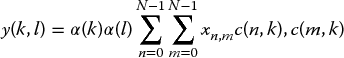
where c(n, k) = cos (2n + l)πk/2N and c(m, k) = cos (2m + l)πk/2N, and the indices k and l range from 0 to N − 1 inclusive. The values a(k) and a(l) are scaling variables. Typically, the separable property of the function is exploited, to allow it to be decomposed into two successive lD transforms; this is achieved using techniques such as row–column decomposition which requires a matrix transposition function between the two one-dimensional (1D) transforms (Sun et al. 1989).
The equation for an N-point 1D transform, which relates an input data sequence x(i), i = 0…N − 1, to the transformed values Y(k), k = 0…N − 1, is given by

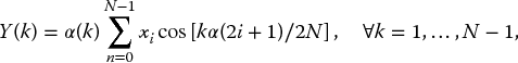
where ![]() , otherwise
, otherwise ![]() . This reduces the number of coefficients to only seven. Equations (6.6) and (6.7) can be broken down into a matrix–vector computation. This yields
. This reduces the number of coefficients to only seven. Equations (6.6) and (6.7) can be broken down into a matrix–vector computation. This yields

where C(k) = cos (2πk/32).
In the form described above, 64 multiplications and 64 additions are needed to compute the 1D DCT but these can be reduced by creating a sparse matrix by manipulating the terms in the input vector on the right.
In its current form the matrix–vector computation would require 64 multiplications and 63 additions to compute the 1D DCT or Y vector. However, a lot of research work has been undertaken to reduce the complexity of the DCT by pre-computing the input data in order to reduce the number of multiplications. One such approach proposed by Chen et al. (1977) leads to

These types of optimizations are possible and a range of such transformations exist for the DCT for both the 1D version (Hou 1987; Lee 1984; Sun et al. 1989) and the direct 2D implementation (Duhamel et al. 1990; Feig and Winograd 1992; Haque 1985; Vetterli 1985), one of which is given by

where

The introduction of zero terms within the matrix corresponds to a reduction in multiplications at the expense of a few extra additions. Furthermore, it gives a regular circuit architecture from this matrix computation as shown in Figure 6.10. Each of the multiplications is a fixed-coefficient multiplication.

Figure 6.10 DCT circuit architecture
The DCT has been surpassed in recent years by the wavelet transform (Daubechies 1990) which transforms the input signal into a series of wavelets. It exploits the fact that the signal is not stationary and that not all frequency components are available at once. By transforming into a series of wavelet, better compression can be achieved. As with the FIR filter and transform examples, only a limited range of functionality is needed and various folding transforms can be used to get the best performance (Shi et al. 2009).
6.4.3 Fixed-Coefficient FPGA Techniques
As was described earlier, a fully programmable MAC functionality is provided by FPGA vendors. In some DSP applications, however, and also in smaller FPGAs which have limited DSP hardware resources, there may be a need to use the underlying programmable hardware resources. There are a number of efficient methods that can perform a multiplication of a stream of data by a single coefficient or a limited range of coefficients giving high speed, but using smaller of resources when compared to a full multiplier implementation in programmable hardware.
In a processor implementation, the requirement to perform a multiplicative operation using a limited range of coefficients, or indeed a single one, has limited performance impact, due to the way the data are stored. However, in FPGA implementations, there is considerable potential to alter the hardware complexity needed to perform the task. Thus, dedicated coefficient multiplication or fixed- or constant-coefficient multiplication (KCM) has considerable potential to reduce the circuitry overhead. A number of mechanisms have been used to derive KCMs. These includes DA (Goslin 1995; Goslin and Newgard 1994), string encoding and common sub-expression elimination (Cocke 1970; Feher 1993).
This concept translated particularly well to the LUT-based and dedicated fast adder structures which can be used for building these types of multipliers; thus an area gain was achieved in implementing a range of these fixed-coefficient functions (Goslin and Newgard 1994; Peled and Liu 1974). A number of techniques have evolved for these fixed-coefficient multiplications and whilst a lot of FPGA architectures have dedicated multiplicative hardware on-board in the form of dedicated multipliers or DSP blocks, it is still worth briefly reviewing the approaches available. The section considers the use of DA which is used for single fixed-coefficient multiplication (Peled and Liu 1974) and also the RCM approach which can multiply a range of coefficient values (Turner and Woods 2004).
The aim is to use the structure which best suits the algorithmic requirements. Initially, DA was used to create FPGA implementations that use KCMs, but these also have been extended to algorithms that require a small range of coefficient values. However, the RCM is a technique that has been particularly designed to cope with a limited range of coefficients. Both of these techniques are discussed in the remaining sections of this chapter.
6.5 Distributed Arithmetic
Distributed arithmetic is an efficient technique for performing multiply-and-add in which the multiplication is reorganized such that multiplication and addition and performed on data and single bits of the coefficients at the same time. The technique is based on the assumption that we will store the computed values rather than carry out the computation (as FPGAs have a readily supply of LUTs).
6.5.1 DA Expansion
Assume that we are computing the sum of products computation in
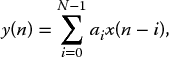
where the values x(i) represent a data stream and the values a0, a1, …, aN − 1 represent a series of coefficient values. Rather than compute the partial products using AND gates, we can use LUTs to generate these and then use fast adders to compute the final multiplication. An example of an eight-bit LUT-based multiplier is given in Figure 6.11; it can seen that this multiplier would require 4 kB of LUT memory resource, which would be considerable. For the multiplicand, MD, MD0 − 7 is the lower eight bits and MD8 − 15 is the higher eight bits. The same idea is applied to the multiplier, MR.

Figure 6.11 LUT-based 8-bit multiplier
The memory requirement is vastly reduced (to 512 bits for the eight-bit example) when the coefficients are fixed, which now makes this an attractive possibility for an FPGA architecture. The obvious implementation is to use a LUT-based multiplier circuit such as that in Figure 6.11 to perform the multiplication a0x(0). However, a more efficient structure results by employing DA (Meyer-Baese 2001; Peled and Liu 1974; White 1989). In the following analysis (White 1989), it should be noted that the coefficient values a0, a1, …, aN − 1 are fixed. Assume the input stream x(n) is represented by a 2’s-complement signed number which would be given as

where xj(n).2j denotes the jth bit of x(n) which in turn is the nth sample of the stream of data x. The term x0(n) denotes the sign bit and so is indicated as negative in the equation. The data wordlength is thus M bits. The computation of y can then be rewritten as

Multiplying out the brackets, we get

The fully expanded version of this is

Reordering, we get

and once again the expanded version gives a clearer idea of how the computation has been reorganized:

Given that the coefficients are now fixed values, the term ∑N − 1i = 0aixi(n) in equation (6.16) has only 2K possible values and the term ∑N − 1i = 0ai( − x0(n)) has only 2K possible values. Thus the implementation can be stored in a LUT of size 2 × 2K bits which, for the earlier eight-bit example, would represent 512 bits of storage.
This then shows that if we use the x inputs as the addresses to the LUT, then the stored values are those shown in Table 6.4. By rearranging the equation

to achieve the representation

we see that the contents of the LUT for this calculation are simply the inverse of those stored in Table 6.2 and can be performed by subtraction rather than addition for the 2’s-complement bit. The computation can either be performed using parallel hardware or sequentially, by rotating the computation around an adder, as shown in Figure 6.12 where the final stage of computation is a subtraction rather than addition.

Figure 6.12 DA-based multiplier block diagram
Table 6.4 LUT contents for DA computation
| Address | ||||
| x03 | x02 | x01 | x00 | LUT contents |
| 0 | 0 | 0 | 0 | 0 |
| 0 | 0 | 0 | 1 | a0 |
| 0 | 0 | 1 | 0 | a1 |
| 0 | 0 | 1 | 0 | a1 + a0 |
| 0 | 1 | 0 | 0 | a2 |
| 0 | 1 | 0 | 1 | a2 + a0 |
| 0 | 1 | 1 | 0 | a2 + a1 |
| 0 | 1 | 1 | 0 | a2 + a1 + a0 |
| 1 | 0 | 0 | 0 | a3 |
| 1 | 0 | 0 | 1 | a3 + a0 |
| 1 | 0 | 1 | 0 | a3 + a1 |
| 1 | 0 | 1 | 0 | a3 + a1 + a0 |
| 1 | 1 | 0 | 0 | a3 + a2 |
| 1 | 1 | 0 | 1 | a3 + a2 + a0 |
| 1 | 1 | 1 | 0 | a3 + a2 + a1 |
| 1 | 1 | 1 | 0 | a3 + a2 + a1 + a0 |
6.5.2 DA Applied to FPGA
It is clear that this computation can be performed using the basic CLB structure of the earlier Xilinx XC400 and early Virtex FPGA families and the logic element in the earlier Altera families where the four-bit LUT is used to store the DA data; the fast adder is used to perform the addition and the data are stored using the flip-flop. In effect, a CLB can perform one bit of the computation meaning that now only eight LUTs are needed to perform the computation, admittedly at a slower rate than a parallel structure, due to the sequential nature of the computation. The mapping effectiveness is increased as the LUT size is increased in the later FPGA families.
This technique clearly offers considerable advantages for a range of DSP functions where one part of the computation is fixed. This includes some fixed FIR and IIR filters, a range of fixed transforms, namely the DCT and FFT, and other selected computations. The technique has been covered in detail elsewhere (Meyer-Baese 2001; Peled and Liu 1974; White 1989), and a wide range of application notes are available from each FPGA vendor on the topic.
6.6 Reduced-Coefficient Multiplier
The DA approach has enjoyed considerable success and was the focal point of the earlier FPGA technologies in DSP computations. However, the main limitation of the technique is that the coefficients must be fixed in order to achieve the area reduction gain. If some applications require the full coefficient range then a full programmable multiplier must be used, which in earlier devices was costly as it had to be built of existing LUT and adder resources, but in more recent FPGA families has been provided in the form of dedicated DSP blocks. However, in some applications such as the DCT and FFT, there is the need for a limited range of multipliers.
6.6.1 DCT Example
Equation (6.9) can be implemented with a circuit where a fully programmable multiplier and adder combination are used to implement either a row or a column, or possibly the whole circuit. However, this is inefficient as the multiplier uses only four separate values at the multiplicand, as illustrated by the block diagram in Figure 6.13. This shows that ideally a multiplier is needed which can cope with four separate values. Alternatively, a DA approach could be used where 32 separate DA multipliers are used to implement the matrix computation. In this case, eight DA multipliers could be used, thereby achieving a reduction in hardware, but the dataflow would be complex in order to load the correct data at the correct time. It would be much more attractive to have a multiplier of the complexity of the DA multiplier which would multiply a limited range of multiplicands, thereby trading hardware complexity off against computational requirements, which is exactly what is achieved in the RCM multipliers (Turner and Woods 2004). The subject is treated in more detail elsewhere (Kumm 2016).

Figure 6.13 Reduced-complexity multiplier
6.6.2 RCM Design Procedure
The previous section on DA highlighted how the functionality could be mapped into a LUT-based FPGA technology. In effect, if you view the multiplier as a structure that generates the product terms and then uses an adder tree to sum the terms to produce a final output, then the impact of having fixed coefficients and organizing the computation as proposed in DA allows one to map a large level of functionality of the product term generator and adder tree within the LUTs. In essence, this is where the main area gain to be achieved.
The concept is illustrated in Figure 6.14, although it is a little bit of illusion as the actual AND and adder operations are not actually generated in hardware, but will have been pre-computed. However, this gives us an insight into how to map additional functionality onto LUT-based FPGAs, which is the core part of the approach.

Figure 6.14 DA-based multiplier block diagram. Source: Turner 2004. Reproduced with permission of IEEE.
In the DA implementation, the focus was to map as much as possible of the adder tree into the LUT. If we consider mapping a fixed-coefficient multiplication into the same CLB capacity, then the main requirement is to map the EXOR function for the fast carry logic into the LUT. This will not be as efficient as the DA implementation, but now the spare inputs can be used to implement additional functionality, as shown by the various structures of Figure 6.15. This is the starting point for the creation of the structures for realizing a plethora of circuits.

Figure 6.15 Possible implementations using multiplexer-based design technique. Source: Turner 2004. Reproduced with permission of IEEE
Figure 6.15(a) implements the functionality of A + B or A + C, Figure 6.15(b) implements the functionality of A − B or A − C, and Figure 6.15(c) implements the functionality of A + B or A − C. This leads to the concept of the generalized structure of Figure 6.16, and Turner (2002) gives a detailed treatment of how to generate these structures automatically, based on an input of desired coefficient values. However, here we use an illustrative approach to show how the functionality of the DCT example is mapped using his technique, although it should be noted that this is not the technique used in Turner (2002).

Figure 6.16 Generalized view of RCM technique
Some simple examples are used to demonstrate how the cells given in Figure 6.15 can be connected together to build multipliers. The circuit in Figure 6.17 multiplies an input by two coefficients, namely 45 and 15. The notation x × 2n represents a left-shifting by n. The circuit is constructed from two 2n ± 1 cascaded multipliers taking advantage of 45 × x and 15 × x having the common factor of 5 × x. The first cell performs 5 × x and then the second cell performs a further multiplication by 9 or 3, by adding a shifted version by 2 (21) or by 8 (23), depending on the multiplexer control signal setting (labeled 15/45). The shifting operation does not require any hardware as it can be implemented in the FPGA routing.

Figure 6.17 Multiplication by either 45 or 15
Figure 6.18 gives a circuit for multiplying by 45 or the prime number, 23. Here a common factor cannot be used, so a different factorization of 45 is applied, and a subtracter is used to generate multiplication by 15 (i.e. 16 − 1), needing only one operation as opposed to three. The second cell is set up to add a multiple of the output from the first cell, or a shifted version of the input X. The resulting multipliers implement the two required coefficients in the same area as a KCM for either coefficient, without the need for reconfiguration. Furthermore, the examples give some indication that there are a number of different ways of mapping the desired set of coefficients and arranging the cells in order to obtain an efficient multiplier structure.

Figure 6.18 Multiplication by either 45 or 23
Turner and Woods (2004) have derived a methodology for achieving the best solution, for the particular FPGA structure under consideration. The first step involves identifying the full range of cells of the type shown in Figure 6.15. Those shown only represent a small sample for the Xilinx Virtex-II range. The full range of cells depends on the number of LUT inputs and the dedicated hardware resource. The next stage is then to encode the coefficients to allow the most efficient structure to be identified, which was shown to be signed digit (SD) encoding. The coefficients are thus encoded and resulting shifted signed digits (SSD) then grouped to develop the tree structure for the final RCM circuit.
6.6.3 FPGA Multiplier Summary
The DA technique has been shown to work well in applications where the coefficients have fixed functionality in terms of fixed coefficients. As can be seen from Chapter 2, this is not just limited to fixed-coefficient operations such as fixed-coefficient FIR and IIR filtering, but can be applied in fixed transforms such as the FFT and DCT. However, the latter RCM design technique provides a better solution as the main requirement is to develop multipliers that multiply a limited range of coefficients, not just a single value. It has been demonstrated for a DCT and a polyphase filter with a comparable quality in terms of performance for implementations based on DA techniques rather than other fixed DSP functions (Turner 2002; Turner and Woods 2004).
It must be stated that changes in FPGA architectures, primarily the development of the DSP48E2 block in Xilinx technologies, and the DSP function blocks in the latest Altera devices, have reduced the requirement to build fixed-coefficient or even limited-coefficient-range structures as the provision of dedicated multiplier-based hardware blocks results in much superior performance. However, there may still be instances where FPGA resources are limited and these techniques, particularly if they are used along with pipelining, can result in implementations of the same speed performance as these dedicated blocks. Thus, it is useful to know that these techniques exist if the DSP expert requires them.
6.7 Conclusions
The chapter has aimed to cover some techniques that specifically look at mapping DSP systems onto specific FPGA platforms. Many will argue that, in these days of improving technology and the resulting design productivity gap, we should move away from this aspect of the design approach altogether. Whilst the sentiment is well intentioned, there are many occasions when the detailed implementation has been important in realizing practical circuit implementations.
In image processing implementations, as the design example in Figure 6.6 indicated, the derivation of a suitable hardware architecture is predicated on the understanding of what the underlying resources are, both in terms of speed and size. Thus a clear understanding of the practical FPGA limitations is important in developing a suitable architecture. Some of the other fixed-coefficient techniques may be useful in applications where hardware is limited and users may wish to trade off the DSP resource against other parts of the application.
Whilst it has not been specifically covered in this chapter, a key aspect of efficient FPGA implementation is the development of efficient design styles. A good treatment of this was given by Keating and Bricaud (1998). Their main aim was to highlight a number of good design styles that should be incorporated in the creation of efficient HDL code for implementation on SoC platforms. In addition to indications for good HDL coding, the text also offered some key advice on mixing clock edges, developing approaches for reset and enabling circuitry and clock gating. These are essential, but it was felt that the scope of this book was to concentrate on the generation of the circuit architecture from a high level.
Bibliography
- Chen WA, Harrison C, Fralick SC 1977 A fast computational algorithm for the discrete cosine transform. IEEE Trans. on Communications, 25(9), 1004–1011.
- Cocke J 1970 Global common subexpression elimination. Proc. Symp. on Compiler Construction, Sigplan Notices 5(7), 1970, pp. 20–24.
- Cooley JW, Tukey JW 1965 An algorithm for the machine computation of the complex Fourier series. Mathematics of Computation, 19, 297–301.
- Daubechies I 1990 The wavelet transform, time-frequency localization and signal analysis. IEEE Trans. on Information Theory 36(5), 961–1005.
- Duhamel P, Guillemot C, Carlach J 1990 A DCT chip based on a new structured and computationally efficient DCT algorithm. In Proc. IEEE Int. Symp. on Circuits and Systems, 1, pp. 77–80.
- Feher B 1993 Efficient synthesis of distributed vector multipliers. In Proc. Elsevier Symposium on Microprocessing and Microprogramming, 38(1–5), pp. 345–350.
- Feig E, Winograd S 1992 Fast algorithms for the discrete cosine transform. IEEE Trans. on Signal Processing 40(9), 2174–2193.
- Goslin G 1995 Using Xilinx FPGAs to design custom digital signal processing devices. Proc. of the DSPX, pp. 565–604.
- Goslin G, Newgard B 1994 16-tap, 8-bit FIR filter applications guide. Xilinx Application note. Version 1.01. Available from http://www.xilinx.com (accessed June 11, 2015).
- Haque MA 1985 A two-dimensional fast cosine transform. IEEE Trans. on Acoustics, Speech, and Signal Processing, 33(6), 1532–1539.
- Hou HS 1987 A fast recursive algorithm for computing the discrete cosine transform. IEEE Trans. on Acoustics, Speech, and Signal Processing, 35(10), 1455–1461.
- Keating M and Bricaud P 1998 Reuse Methodology Manual for System-On-A-Chip Designs. Kluwer Academic Publishers, Norwell, MA.
- Lee BG 1984 A new algorithm to compute the discrete cosine transform. IEEE Trans. on Acoustics, Speech and Signal Processing 32(6), 1243–1245.
- Kumm M 2016 Multiplication Optimizations for Field Programmable Gate Arrays. Springer Vieweg, Wiesbaden.
- Meyer-Baese U 2001 Digital Signal Processing with Field Programmable Gate Arrays. Springer, Berlin.
- Natarajan T, Rao KR 1974 Discrete cosine transform. IEEE Trans. on Computers, 23(1), 90–93.
- Peled A, Liu B 1974 A new hardware realisation of digital filters. IEEE Trans. on Acoustics, Speech and Signal Processing, 22(6), 456–462.
- Shi G, Liu W, Zhang L, Li F 2009 An efficient folded architecture for lifting-based discrete wavelet transform. IEEE Trans. on Circuits and Systems II: Express Briefs, 56(4), 290–294.
- Sun MT, Chen TC, Gottlieb AM 1989 VLSI implementation of a 16x16 discrete cosine transform. IEEE Trans. on Circuits and Systems, 36(4), 610–617.
- Turner RH 2002 Functionally diverse programmable logic implementations of digital processing algorithms. PhD thesis, Queen’s University Belfast.
- Turner RH, Woods R, Courtney T 2002 Multiplier-less realization of a poly-phase filter using LUT-based FPGAs. In Proc. Int. Conf. on Field Programmable Logic and Application, pp. 192–201.
- Turner RH, Woods R 2004 Highly efficient, limited range multipliers for LUT-based FPGA architectures. IEEE Trans. on VLSI Systems 12(10), 1113–1118.
- Vaidyanathan PP 1990 Multirate digital filters, filter banks, polyphase networks, and applications: a tutorial. Proc. of the IEEE, 78(1), 56–93.
- Vetterli M 1985 Fast 2-D discrete cosine transform. In Proc. IEEE Conf. Acoustics, Speech and Signal Processing, pp. 1538–1541.
- Wenzler A, Lueder E 1995 New structures for complex multipliers and their noise analysis. In Proc. IEEE Int. Symp. on Circuits and Systems, 2, pp. 1432–1435.
- White SA 1989 Applications of distributed arithmetic to digital signal processing. IEEE Acoustics, Speech and Signal Processing Magazine, 6(3), 4–19.
- Xilinx Inc. 2015 UltraScale Architecture Configurable Logic Block: User Guide. UG574 (v1.2). Available from http://www.xilinx.com (accessed June 11, 2015).