4
Technology Review
4.1 Introduction
The technology used for DSP implementation is very strongly linked to the astonishing developments in silicon technology. As was highlighted in the introduction to this book, the availability of a transistor which has continually decreased in cost has been the major driving force in creating new markets and has overseen the development of a number of DSP technologies. Silicon technology has offered an increasingly cheaper platform, and has done so at higher speeds and at a lower power cost. This has inspired a number of core markets, such as computing, mobile telephony and digital TV.
As Chapter 2 clearly indicated, there are numerous advantages for digital systems, specifically guaranteed accuracy, essentially perfect reproducibility and better aging; these developments are seen as key to the continued realization of future systems. The earliest DSP filter circuits were pioneered by Leland B. Jackson and colleagues at Bell Laboratories in the late 1960s and early 1970s (see Jackson 1970). At that time, the main aim was to create silicon chips to perform basic functions such as FIR and IIR filtering. A key aspect was the observation that the binary operation of the transistor was well matched to digital operations required in DSP systems.
From these early days, a number of technologies emerged, ranging from simple microcontrollers which can process systems with sampling rates typically in the moderate kilohertz range, right through to dedicated SoC solutions that give performance in the teraOPS region. The processor style architecture has been exploited in various forms, ranging from single- to multicore processor implementations, DSP microprocessors with dedicated hardware to allow specific DSP functionality to be realized efficiently, and reconfigurable processor architectures. Specialized DSP functionality has also been added to conventional central processing units (CPUs) and application-specific instruction processors (ASIPs) that are used for specific markets. All of these are briefly discussed in this chapter with the aim of giving a perspective against which FPGAs should be considered.
The major change between this chapter and its first edition counterpart concerns microprocessors: there has been a major development in architectures, particularly with the evolution of the Intel multicore and Xeon Phi, resulting in a body of work on parallel programming (Reinders and Jeffers 2014). In addition, multicore DSP architectures have evolved. Finally, graphical processing units (GPUs) are also included as they are now being widely used in many other fields than graphics including DSP. As Chapter 5 is dedicated to the variety of FPGA architectures, the FPGA perspective is only alluded to. Major themes include level of programmability, the programming environment (including tools, compilers and frameworks), the scope for optimization of specifically DSP functionality on the required platform, and the quality of the resulting designs in terms of area, speed, throughput, power and even robustness.
Section 4.2 starts with some remarks on silicon technology scaling and how Dennard scaling has broken down, leading to the evolution of parallelism into conventional DSP platforms. Section 4.3 outlines some further thoughts on architecture and programmability and gives some insights towards the performance limitations of the technologies, and also comments on the importance of programmability. In Section 4.4 the functional requirements of DSP systems are examined, highlighting issues such as computational complexity, parallelism, data independence and arithmetic advantages. The section ends with a brief definition of technology classification and introduces concepts of single instruction, multiple data (SIMD) and multiple instruction, multiple data (MIMD). This is followed by a brief description of microprocessors in Section 4.5 with some more up-to-date description of multicore architectures. DSP processors are then introduced in Section 4.6 along with some multicore examples. Section 4.7 is a new section on GPUs as these devices have started to be used in some DSP applications. For completeness, solutions based on the system-on-chip (SoC) are briefly reviewed in Section 4.8, which includes the development of parallel machines including systolic array architectures. A core development has been the partnering of various technologies, namely ARM processors and DSP microprocessors, and ARM processors incorporated in FPGA fabrics. A number of examples of this evolution are given in Section 4.9. Section 4.10 gives some thoughts on how the various technologies compare and sets the scene for FPGAs in the next chapter.
4.2 Implications of Technology Scaling
Since the first edition of this book, there has been a considerable shift in the direction of evolution of silicon, largely driven by concerns in silicon scaling. Dennard’s law builds on Moore’s law, relating how the performance of computing is growing exponentially at roughly the same rate as Moore’s law. This was driven by the computing and supercomputing industries and therefore, by association, refers to DSP technologies.
The key issue is that Dennard’s law is beginning to break down as many computing companies are becoming very concerned by the power consumption of their devices and beginning to limit power consumption for single devices to 130 W (Sutter 2009). This is what Intel has publicly declared. To achieve this power capping requires a slowdown in clock scaling. For example, it was predicted in the 2005 of ITRS Roadmap (ITRS 2005) that clock scaling would continue and we would have expected to have a clock rate of 30 GHz today (ITRS 2011). This was revised in 2007 to 10 GHz, and then in 2011 to 4 GHz, which is what is currently offered by computing chip companies. The implications of this are illustrated in Figure 4.1 reproduced from Sutter (2009).

Figure 4.1 Conclusions from Intel CPU scaling

Figure 4.2 Simple parallel implementation of a FIR filter
Moore’s law has continued unabated, however, in terms of number of devices on a single silicon die, so companies have acted to address the shortfall in clock scaling by shifting towards parallelism and incorporating multiple devices on a single die. As will be seen later, this has implications for the wider adaption of FPGAs because as the guaranteed clock rate ratio of CPUs over FPGAs is considerably reduced, the performance divide widens, making FPGAs an attractive proposition. This would seem to be reflected in the various developments of computing companies in exploiting FPGA technologies largely for data centers where the aim is to be able to reduce the overall power consumption costs, as described in the next chapter.
The authors argue that the main criterion in DSP system implementation is the circuit architecture that is employed to implement the system, i.e. the hardware resources available and how they are interconnected; this has a major part to play in the performance of the resulting DSP system. FPGAs allow this architecture to be created to best match the algorithmic requirements, but this comes at increased design cost. It is interesting to compare the various approaches, and this chapter aims to give an overview of the various technologies available for implementing DSP systems, using relevant examples where applicable, and the technologies are compared and contrasted.
4.3 Architecture and Programmability
In many processor-based systems, design simply represents the creation of the necessary high-level code with some thought given to the underlying technology architecture, in order to optimize code quality and thus improve performance. Crudely speaking, though, performance is sacrificed to provide this level of programmability. Take, for example, the microprocessor architecture based on the von Neumann sequential model where the underlying architecture is fixed and the maximum achievable performance will be determined by efficiently scheduling the algorithmic requirements onto the inherently sequential processing architecture. If the computation under consideration is highly parallel in nature (as is usually the case in DSP), then the resulting performance will be poor.
If we were to take the other extreme and develop an SoC-based architecture that best matches the parallelism of computational complexity of the algorithm (as will be outlined in the final section of this chapter), then the best performance in terms of area, speed and power consumption should be achieved. This requires a number of design activities to ensure that hardware implementation metrics best match the application performance criteria and that the resulting design operates correctly.
To more fully understand this concept of generating a circuit architecture, consider the “state of the art” in 1969. Hardware capability in terms of numbers of transistors was limited and thus highly valued, so the processing in the filters described in Jackson (1970) had to be undertaken in a rather serial fashion. Current FPGA technology provides hundreds of bit parallel multipliers, so the arithmetic style and resulting performance are quite different, implying a very different sort of architecture. The aim is thus to make the best use of the available hardware against the performance criteria of the application. Whilst this approach of developing the hardware to match the performance needs is highly attractive, the architecture development presents a number of problems related to the very process of producing this architecture, namely design time, verification and test of the architecture in all its various modes, and all the issues associated with producing a design that is right first time.
Whilst the implementation of these algorithms on a specific hardware platform can be compared in terms of metrics such as throughput rate, latency, circuit area, energy, and power consumption, one major theme that can also be used to differentiate these technologies is programmability (strictly speaking, ease of programmability). As will become clear in the descriptive material in this section, DSP hardware architectures can vary in their level of programmability. A simple platform with a fixed hardware architecture can then be easily programmed using a high-level software language as, given the fixed nature of the platform, efficient software compilers can be (and indeed have been) developed to create the most efficient realizations. However, as the platform becomes more complex and flexible, the complexity and efficiency of these tools are compromised, as now special instructions have to be introduced to meet this functionality and the problem of parallel processing rears its ugly head.
In this case, the main aim of the compiler is to take source code that may not have been written for the specific hardware architecture, and identify how these special functions might be applied to improve performance. In a crude sense, we suggest that making the circuit architecture programmable achieves the best efficiency in terms of performance, but presents other issues with regard to evolution of the architecture either to meet small changes in applications requirements or relevance to similar applications. This highlights the importance of tools and design environments, described in Chapter 7.
SoC is at the other end of the spectrum from a programmability perspective; in this case, the platform will have been largely developed to meet the needs of the system under consideration or some domain-specific, standardized application. For example, OFDM access-based systems such as LTE-based mobile phones require specific DSP functionality such as orthogonal frequency division multiple access (OFDMA) which can be met by developing an SoC platform comprising processors and dedicated hardware IP blocks. This is essential to meet the energy requirements for most mobile phone implementations. However, silicon fabrication costs have now pushed SoC implementation into a specialized domain where typically solutions are either for high volume, or have specific domain requirements, e.g. ultra-low power in low- power sensors.
4.4 DSP Functionality Characteristics
DSP operations are characterized as being computationally intensive, exhibiting a high degree of parallelism, possessing data independence, and in some cases having lower arithmetic requirements than other high-performance applications, e.g. scientific computing. It is important to understand these issues more fully in order to judge their impact for mapping DSP algorithms onto hardware platforms such as FPGAs.
4.4.1 Computational Complexity
DSP algorithms can be highly complex. For example, consider the N-tap FIR filter expression given in Chapter 2 and repeated here:

In effect, this computation indicates that a0 must be multiplied by x(n), followed by the multiplication of a1 by x(n − i) to which it must be added, and so on. Given that the tap size is N, this means that the computation requires N multiplications followed by N − 1 additions in order to compute y(n) as shown below:
Given that another computation will start on the arrival of next sample, namely xn + 1, this defines the computations required per cycle, namely 2N operations (N multiplications and N additions) per sample or two operations per tap. If a processor implementation is targeted, then this requires, say, a loading of the data every cycle, which would need two or three cycles (to load data and coefficients) and storage of the accumulating sum. This could mean an additional three operations per cycle, resulting in six operations per tap or, overall, 6N operations per sample. For an audio application with a sampling rate of 44.2 kHz, a 128-tap filter will require 33.9 MSPS, which may seem realistic for some technologies, but when you consider image processing rates of 13.5 MHz, these computational rates quickly explode, resulting in a computation rate of 10 gigasamples per second (GSPS). In addition, this may only be one function within the system and thus represent only a small proportion of the total processing required.
For a processor implementation, the designer will determine if the hardware can meet the throughput requirements by dividing the clock speed of the processor by the number of operations that need to be performed each cycle, as outlined above. This can give a poor return in performance, since if N is large, there will be a large disparity between clock and throughput rates. The clock rate may be fast enough to provide the necessary sampling rate, but it will present problems in system design, both in delivering a very fast clock rate and controlling the power consumption, particularly dynamic power consumption, as this is directly dependent on the clock rate.
4.4.2 Parallelism
The nature of DSP algorithms is such that high levels of parallelism are available. For example, the expression in equation (4.1) can be implemented in a single processor, or a parallel implementation, as shown in Figure 4.1, where each element in the figure becomes a hardware component therefore implying 127 registers for the delay elements, 128 MAC blocks for computing the products, a1x(N − i), where i = 0, 1, 2, …, N − 1, and their addition which can of course, be pipelined if required.
In this way, we have the hardware complexity to compute an iteration of the algorithm in one sampling period. Obviously, a system with high levels of parallelism and the needed memory storage capability will accommodate this computation in the time necessary. There are other ways to derive the required levels of parallelism to achieve the performance, outlined in Chapter 8.
4.4.3 Data Independence
The data independence property is important as it provides a means for ordering the computation. This can be highly important in reducing the memory and data storage requirements. For example, consider N iterations of the FIR filter computation of equation (4.1), below. It is clear that the x(n) datum is required for all N calculations and there is nothing to stop us performing the calculation in such a way that N computations are performed at the same time for y(n), y(n + 1), …, y(n + N − 1), using the x(n) datum and thus removing any requirement to store it:

Obviously the requirement is now to store the intermediate accumulator terms. This obviously presents the designer with a number of different ways of performing system optimization, and in this case gives in a variation of schedule in the resulting design. This is just one implication of data independence.
4.4.4 Arithmetic Requirements
In many DSP technologies, the wordlength requirements of the input data are such that the use of internal precision can be considerably reduced. For example, consider the varying wordlengths for the different applications as illustrated at the end of Chapter 3. Typically, the input wordlength will be determined by the precision of the ADC device creating the source material. Depending on the amount and type of computation required (e.g. multiplicative or additive), the internal word growth can be limited, which may mean that a suitable fixed-point realization is sufficient.
The low arithmetic requirement is vital as it means small memory requirements, faster implementations as adder and multiplier speeds are governed by input wordlengths, and smaller area. For this reason, there has been a lot of work to determine maximum wordlengths as discussed in the previous chapter. One of the interesting aspects is that for many processor implementations both external and internal wordlengths will have been predetermined when developing the architecture, but in FPGAs it may be required to carry out detailed analysis to determine the wordlength at different parts of the DSP system (Boland and Constantinides 2013).
All of these characteristics of DSP computation are vital in determining an efficient implementation, and have in some cases driven technology evolution. For example, one the main differences between the early DSP processors and microprocessors was the availability of a dedicated multiplier core. This was viable for DSP processors as they were targeted at DSP applications where multiplication is a core operation, but not for general processing applications, and so multipliers were not added to microprocessors at that time.
4.4.5 Processor Classification
The technology for implementing DSP ranges from microcontrollers right though to single-chip DSP multi-processors, which range from conventional processor architectures with a very long instruction word (VLIW) extension to allow instruction-level parallelism through to dedicated architecture defined for specific application domains. Although there have been other more comprehensive classifications after it, Flynn’s classification is the most widely known and used for identifying the instructions and the data as two orthogonal streams in a computer. The taxonomy is summarized in Table 4.1, which includes single instruction, single data (SISD) and multiple instruction, single data (MISD). These descriptions are used widely to describe the various representations for processing elements (PEs).
Table 4.1 Flynn’s taxonomy of processors
| Class | Description | Examples |
SISD |
Single instruction stream operating | von Neumann |
| on single data stream | processor | |
SIMD |
Several PEs operating in lockstep | VLIW processors |
| on individual data streams | ||
MISD |
Few practical | |
| examples | ||
MIMD |
Several PEs operating independently | Multi-processor |
| on separate data streams |
4.5 Microprocessors
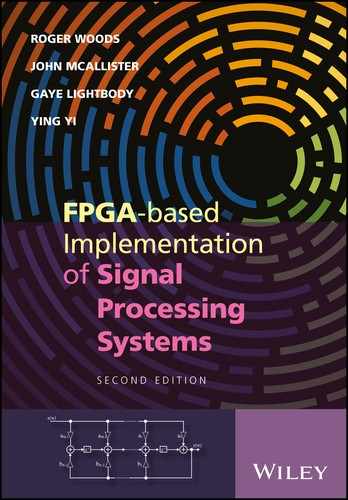
The classical von Neumann microprocessor architecture is shown in Figure 4.3. This sequentially applies a variety of instructions to specified data in turn. The architecture consists of five types of unit: a memory containing data and instructions, an instruction fetch and decode (IFD) instruction, arithmetic logic unit (ALU) and the memory access (MA) unit. These units correspond to the four different stages of processing, which repeat for every instruction executed on the machine:
- Instruction fetch
- Instruction decode
- Execute
- Memory access.
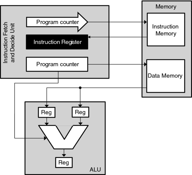
Figure 4.3 Von Neumann processor architecture
During the instruction fetch (IF) stage, the IFD unit loads the instruction at the address in the program counter (PC) into the instruction register (IR). In the second, instruction decode (ID) stage, this instruction is decoded to produce an opcode for the ALU and the addresses of the two data operands, which are loaded into the input registers of the ALU. During the execute stage, the ALU performs the operation specified by the opcode on the input operands to produce the result, which is written back into memory in the MA stage.
In general, these types of SISD machine can be subdivided into two categories, depending on their instruction set style. The complex instruction set computer (CISC) machines have complex instruction formats which can become highly specific for specific operations. This leads to compact code size, but can complicate pipelined execution of these instructions. On the other hand, reduced instruction set computer (RISC) machines have regular, simple instruction formats which may be processed in a regular manner, promoting high throughput via pipelining, but will have increased code size.
The von Neumann processor architecture is designed for general-purpose computing, and is limited for embedded applications, due to its highly sequential nature. This makes this kind of processor architecture suitable for a wide range of applications. However, whilst embedded processors must be flexible, they are often tuned to a particular application and have advanced performance requirements, such as low power consumption or high throughput. A key evolution in this area has been the ARM series of processors which have been primarily developed for embedded applications and, in particular, mobile phone applications. More recently they have expanded to the wider internet of things (IoT) markets and also data servers, specifically microservers (Gillan 2014).
4.5.1 ARM Microprocessor Architecture Family
The ARM family of embedded microprocessors are a good example of RISC processor architectures, exhibiting one of the key trademarks of RISC processor architectures, namely that of instruction execution path pipelining. The pipelines of these processor architectures (as identified for the ARM processor family in Table 4.2) are capable of enabling increased throughput of the unit, but only up to a point. A number of innovations have developed as the processor has developed.
- ARM7TDMI has a three-stage pipeline with a single interface to memory.
- ARM926EJ-S has a five-stage pipeline with a memory management unit with various caches and DSP extensions. The DSP extension is in the form of a single-cycle 32 × 16-bit multiplier and supports instructions that are common in DSP architectures, i.e. variations on signed multiply-accumulate, saturated add and subtract, and counting leading zeros.
- ARM1176JZ(F)-S core has moved to a eight-stage pipeline with improved performance in terms of branch prediction, a vector floating-point unit and intelligent energy management.
- ARM11 MPCore technology has moved to multicore and has up to four MP11 processors with cache coherency and an interrupt controller.
- ARM Cortex-A8 has moved to a 14-stage pipeline and has an on-board NEON media processor.
Table 4.2 ARM microprocessor family overview
| Processor | Instruction sets | Extensions |
| ARM7TDMI, | Thumb | |
| ARM922T | ||
| ARM926EJ-S | Improved ARM/Thumb | Jazelle |
| ARM946E-S | DSP instructions | |
| ARM966E-S | ||
| ARM1136JF-S | SIMD instructions | Thumb-2, TrustZonezelle |
| ARM1176JZF-S | Unaligned data support | |
| ARM11 MPCore | ||
| Cortex-A8/R4/M3/M1 | Thumb-2 | v7A (applications) - NEON |
| Thumb-2 | v7R (real-time) - H/W divide | |
| Thumb-2 | V7M (microcontroller) - H/W | |
| Divide & Thumb-2 only |
With increased pipeline depth comes increased control complexity, a factor which places a limit on the depth of pipeline which can produce justifiable performance improvements. After this point, processor architectures must exploit other kinds of parallelism for increased real-time performance. Different techniques and exemplar processor architectures to achieve this are outlined in Section 4.5.2.
The key innovation of the ARM processor is that the company believes that the architecture comprises the instruction set and the programmer’s model. Most ARMs implement two instruction sets, namely the 32-bit ARM instruction set and the 16-bit Thumb instruction set. The Thumb set has been optimized for code density from C code as this represents a very large proportion of example ARM code. It also gives improved performance from narrow memory which is critical in embedded applications.
The latest ARM cores include a new instruction set, Thumb-2, which provides a mixture of 32-bit and 16-bit instructions and maintains code density with increased flexibility. The Jazelle-DBX cores have been developed to allow the users to include executable Java bytecode. A number of innovations targeted at DSP have occurred, e.g. as in the ARM9 family where DSP operations were supported. The evolution in the ARM to support DSP operations has not substantially progressed beyond that highlighted. A more effective route has been to incorporate the ARM processor with both DSP processors, which is discussed in Section 4.9.
ARM Programming Route
The most powerful aspect of microprocessors is the mature design flow that allows programming from C/C++ source files. ARM supports an Eclipse-based Integrated Design Environment (IDE) or IDE-based design flow which provides the user with a C/C++ source editor which helps the designer to spend more time writing code and avoid chasing down syntax errors. The environment will list functions, variables, and declarations, allows full change history and re-factoring of function names and code segments globally. This provides a short design cycle allowing code to be quickly compiled into ARM hardware.
It is clear that there have been some architectural developments which make the ARM processor more attractive for DSP applications, but, as indicated earlier, the preferred route has been a joint offering either with DSP processors or FPGAs. ARM also offers an mbed hardware platform (https://mbed.org/) which uses on-line tools.
4.5.2 Parallella Computer
A clear shift in microprocessors has been towards multicores and there have been many examples of multicore structures, including Intel multicore devices and multicore DSP devices (see later). The Parallella platform is an open source, energy-efficient, high-performance, credit-card sized computer which is based on Adapteva’s Epiphany multicore chips. The Epiphany chip consists of a scalable array of simple RISC processors programmable in C/C++ connected together with a fast on-chip network within a single shared memory architecture. It comes as either a 16- or 64-core chip. For the 16-core system, 1, 2, 3, 4, 6, 8, 9, 12 or 16 cores can be used simultaneously.
The Epiphany is a 2D scalable array of computing nodes which is connected by a low-latency mesh network-on-chip and has access to shared memory. Figure 4.4 shows the Epiphany architecture and highlights the core components:
- a superscalar, floating-point RISC CPU that can execute two floating-point operations and a 64-bit memory load operation on every clock cycle;
- local memory in each mesh node that provides 32 bytes/cycle of sustained bandwidth and is part of a distributed, shared memory system;
- multicore communication infrastructure in each node that includes a network interface, a multi-channel DMA engine, multicore address decoder, and a network monitor;
- a 2D mesh network that supports on-chip node-to-node communication latencies in nanoseconds, with zero startup overhead.

Figure 4.4 Epiphany architecture
The Adapteva processor has been encapsulated in a small, high-performance and low-power computer called the Parallella Board. The main processor is a dual-core ARM A9 and also a Zynq FPGA. The board can run a Linux-based operating system. The main memory of the board is contained in an SD card and this also includes the operating files for the system. There is 1 GB of shared memory between the ARM host processor and the Epiphany coprocessor.
The system is programmed in C/C++, but there are a number of extra commands which are specific to the Parallella Board and handle data transfer between the Epiphany and the ARM host processor. It can be programmed with most of the common parallel programming methods, such as SIMD and MIMD, using parallel frameworks like open computing language (OpenCL) or Open Multi-Processing (OpenMP). Two programs need to be written, one for the host processor and one for the Epiphany itself. These programs are then linked when they are compiled.
Programming Route
The Parallela is programmed by the Epiphany software development kit (SDK), known as eSDK, and is based on standard development tools including an optimizing C-compiler, functional simulator, debugger, and multicore IDE. It can directly implement regular ANSI-C and does not require any C-subset, language extensions, or SIMD style programming. The eSDK interfaces with a hardware abstraction layer (HAL) which allows interaction with the hardware through the user application.
The key issue with programming the hardware is to try to create the program in such a way that the functionality will efficiently use the memory of each core which has an internal memory of 32 kB which is split into four separate 8 kB banks. Also, every core also has the ability to quickly access the memory of the other cores which means that streaming will work effectively as data can then be passed in parallel. The cores also have access to the memory shared with the ARM processor, which suggests a means of supplying input data.
Efficiency is then judged by how effectively the computation can be distributed across each core, so it is a case of ensuring an efficient partition. This will ensure that a good usage of the core functionality can be achieved which preserves the highly regular dataflow of the algorithm so that data passing maps to the memory between cores. This may require a spatial appreciation of the architecture to ensure that the functionality efficiency is preserved and a regular matching occurs. This allow the realization to exploit the fast inter-core data transfers and thus avoid multiple accesses in and out of shared memory.
4.6 DSP Processors
As was demonstrated in the previous section, the sequential nature of microprocessor architectures makes them unsuitable for efficient implementation of complex DSP systems. This has spurred the development of dedicated types of processors called DSP microprocessors such as Texas Instrument’s TMS32010 which have features that are particularly suited for DSP processing. These features have been encapsulated in the Harvard architecture illustrated in Figure 4.5.

Figure 4.5 Processor architectures
The earlier DSP microprocessors were based on the Harvard architecture. This differs from the von Neumann architecture in terms of memory organization and dedicated DSP functionality. In the von Neumann machine, one memory is used for storing both program code and data, effectively providing a memory bottleneck for DSP implementation as the data independence illustrated in Section 4.4.3 cannot be effectively exploited to provide a speedup. In the Harvard architecture, data and program memory are separate, allowing the program to be loaded into the processor independently of the data which is typically streaming in nature.
DSP processors are designed also to have dedicated processing units, which in the early days took the form of a dedicated DSP block for performing multiply-accumulation quickly. In addition, separate data and program memories and dedicated hardware became the cornerstone of earlier DSP processors. Texas Instrument’s TMS32010 DSP (Figure 4.6), which is recognized as the first DSP processor, was an early example of the Harvard architecture and highlights the core features, so it acts as a good example to understand the broad range of DSP processors. In the figure, the separate program and data buses are clearly highlighted. The dedicated hardware unit is clearly indicated in this case as a 16-bit multiplier connected to the data bus which produces a 32-bit output called P32, which can then be be accumulated as indicated by the 32-bit arithmetic logic unit (ALU) and accumulator (ACC) circuitry which is very effective in computing the function given in equation (4.1).

Figure 4.6 TI TMS32010 DSP processor (Reproduced with permission of Texas Instruments Inc.)
4.6.1 Evolutions in DSP Microprocessors
A number of modifications have occurred to the original Harvard DSP architecture, which are listed below (Berkeley Design Technology 2000).
- VLIW. Modern processor architectures have witnessed an increase in the internal bus wordlengths. This allows a number of operations performed by each instruction in parallel, using multiple processing functional units. If successful, the processor will be able to use this feature to exploit these multiple hardware units; this depends on the computation to be performed and the efficiency of the compiler in utilizing the underlying architecture. This is complicated by the move toward higher-level programming languages which require good optimizing compilers that can efficiently translate the high-level code and eliminate any redundancies introduced by the programmer.
- Increased number of data buses. In many recent devices the number of data buses has been increased. The argument is that many DSP operations involve two operands, thus requiring three p1eces of information (including the instruction) to be fed from memory. By increasing the number of buses, a speedup is achieved, but this also increases the number of pins on the device. However, some devices gets around this by using a program cache, thereby allowing the instruction bus to double as a data bus when the program is being executed out of the program cache.
- Pipelining. Whilst the introduction of VLIW has allowed parallelism, another way to exploit concurrency is to introduce pipelining, both within the processing units in the DSP architecture, and in the execution of the program. The impact of pipelining is to break the processing time into smaller units, thereby allowing several overlapping computations to take place at once, in the same hardware. However, this comes at the expense of increased latency. Pipelining can also be employed within the processor control unit which controls the program fetch, instruction dispatch and instruction decode operation.
- Fixed point operations. Some DSP systems only require fixed-point arithmetic and do not need the full-precision arithmetic offered by some DSP processing units. For this reason, fixed-point and floating-point DSP microprocessors have evolved to match application environments. However, even in fixed-point, some applications do not require the full fixed-point range of some processors, e.g. 32 bits in the TMS320C64xx series processor, and therefore inefficiency exists. For example, for a filter application in image processing applications, the input wordlength may vary between 8 and l6 bits, and coefficients could take 12–16 bits. Thus, the multiplication stage will not require anything larger than a 16 × 16-bit multiplier. The DSP processors exploit this by organizing the processing unit, e.g. the TMS320C6678, by allowing multiple multiplications to be take place in one time unit, thereby improving the throughput rate. Thus, the processors are not compromised in terms of the internal wordlength used.
These optimizations have evolved over a number of years. and have led to improved performance. However, it is important to consider the operation in order to understand how the architecture performs in some applications.
4.6.2 TMS320C6678 Multicore DSP
The TMS320C6678 multicore fixed- and floating-point DSP microprocessor is based on TI’s KeyStone multicore architecture and is illustrated in Figure 4.7. It comprises eight C66x CorePac DSPs, each of which runs at 1.0–1.25 GHz, giving an overall clock rate of up to 10 GHz. This gives 320 giga multiply-accumulates (GMAC) at the clock rate of 1.25 GHz. A key aspect has been the introduction of increasing levels of memory in the form of 32 kB of L1 program cache and 32 kB of L1 data cache with 512 kB of L2 cache per core. The chip also has 4 MB of L2 shared memory. Clearly, with technology evolution and in line with processor developments and the response to the slowdown of Dennard scaling (see Section 4.2), the response has been to create a multicore implementation of previous processors in this case, the C6000, rather than scale the processor.

Figure 4.7 TMS320C6678 multicore fixed and floating-point DSP microprocessor
Another feature of the latest DSP families has been the inclusion of specific functionality, specifically network-on-chip topology in the form of a TeraNet switch fabric which support up to 2 TB of data. There are also dedicated processing engines such as packet and security accelerators to address the networking and security markets in which DSP processors are increasingly being used. The devices also come with an additional features such as 64-bit DDR3 and universal asynchronous receiver/transmitter (UART) interfaces.
The key objective is to be able to exploit the processing capability offered by this multicore platform which depends on both the computation to be performed and the use of optimizing compilers that perform a number of simplifications to improve efficiency. These simplifications include routines to remove all functions that are never called and to simplify functions that return values that are never used, to reorder function declarations and propagate arguments into function bodies (Dahnoun 2000). The compiler also performs a number of optimizations to take advantage of the underlying architecture including software pipelining, loop optimizations, loop unrolling and other routines to remove global assignments and expressions (Dahnoun 2000).
4.7 Graphical Processing Units
Another class of processors that has had a major impact is the graphical processing unit (GPU). It was developed particularly to suit applications in image and video processing and as such has resulted in a multi-processor array structure with a memory hierarchy suited to store the initial image data and then portions of the image for highly parallel computing. While originally designed with a fixed pipeline which is highly suitable for graphics, the modern GPU’s pipeline is highly programmable and allows for general-purpose computation. For this reason, the technology has now seen wider adoption. The creation of the general-purpose graphical processing unit (GPUPU) presents a powerful computing platform as it comprises a CPU which computes the sequential part of the code and the GPU calculates the computer-intensive part of the code.
There are many GPUs available from different manufacturers, and all offer massively parallel floating-point computation and high-speed, large-capacity RAM. The Nvidia GeForce GPU is illustrated in Figure 4.8 and shows the computing structure. The architecture is generally composed of a number of floating-point streaming processors (SP) optimized for graphics processing, each of which contains a small amount of low-latency shared memory along with a larger bank of SDRAM which is available to all multi-processors. This is contained with the shared-memory multi-processors (SMP). The architecture allows parallel execution of numerous SIMD functions.

Figure 4.8 Nvidia GeForce GPU architecture
Since products from different manufacturers will inevitably differ in their low-level implementation, there are a number of abstract application programming interfaces (APIs) including CUDA and OpenCL. CUDA can used to program the devices and allow the software developer to access the massively parallel SIMD architecture of modern GPUs for general processing tasks. CUDA was developed by Nvidia and is an extension of C to enable programming of GPU devices; it allows easy management of parallelism and handles communications with the host. OpenCL is a broadly supposed open standard, defined by the Khronos Group, that allows programming of both GPUs and CPUs. It is supported by Intel, AMD, Nvidia, and ARM, and is the GPGPU development platform most widely used by developers in both the USA and Asia-Pacific.
The key aspect of GPU is hundreds of cores that can be used for highly parallel implementation of graphics algorithms and high levels of memory. As numerous computations or threads can run on each processor engine, the GPU has thousands of threads. Because the architecture is fixed and is now being applied to a wider range of applications, the technology is cheap, certainly compared to DSP microprocessor and FPGAs.
4.7.1 GPU Architecture
GPU implementations work well for streaming applications where large amounts of data will be streamed to the GPU and then processed. Obviously this is the case for image and video processing which is what the hardware was developed for in the first instance. When programming the device, it is paramount to consider the architectural implications of the hardware, to produce efficient code. It could be argued to some some extent that this places much more emphasis on the programmer’s ability to get the performance out of the hardware, but this is increasingly the case for multicore technology.
For example, the multi-processors share one off-chip global memory and it is not cached, so it is very important to achieve memory coalescing (Luo et al. 2010). Memory coalescing occurs when consecutive threads access consecutive memory locations. In this case, it is important to coalesce several memory transactions into one transaction, as there is a shared memory within each SMP which is common to all the streaming processors inside the multi-processor. As the shared memory is on chip, it can be accessed within a smaller number of clock cycles, whereas the global memory will be typically an order of magnitude larger.
Thus the memory can be viewed as follows:
- Global memory is typically several gigabytes and is available to the GPU processors. It is used for fast caching to the motherboard RAM, as it is used to read and write large amounts of data and is normally associated with blocks of threads.
- Local shared memory is smaller (tens of kilobytes) and can be accessed extremely quickly, so it can really speed up computations, since the instruction access cost is much lower compared to global memory. It is usually associated with a block of threads
- Private thread memory, as the name suggests, is a very small bank of memory used within each thread for variables and temporary storage during the computation.
By carefully observing the memory structure and ensuring that the computation is inherently parallel enough, it is possible to achieve a speedup. For example, the work on breadth-first search graph operation (Luo et al. 2010) shows that a tenfold increase in the number of vertices computed only incurs a fivefold increase in the compute time. GPUs have also been applied to some DSP algorithms such as the low-density parity-check (LDPC) decoder (Wang et al. 2011). The challenge has been to use the threads to fully occupy the GPU computation resources when decoding the LDPC codes and organizing the computation in such a way as to minimize the memory access times. Work by Falcao et al. (2012) has compared the programming of a GPU and CPU using OpenCL.
4.8 System-on-Chip Solutions
Up to now, the DSP technology offerings have been in the form of some type of predefined architectural offering. The major attraction of dedicated ASIC offerings is that the architecture can be developed to specifically match the algorithmic requirements, allowing the level of parallelism to be created to ultimately match the performance requirements. For the earlier 128-tap FIR filter, it is possible to dedicate a multiplier and adder to each multiplication and addition respectively, thereby creating a fully parallel implementation. Moreover, this can then be pipelined in order to speed up the computation, giving if required an N times speedup for an N-tap filter. How the designer can achieve this is described in detail in Chapter 8.
When considering programmability, SoC solutions will have been developed with programmable parts as well as dedicated acceleration blocks. Indeed, the C6000 DSP described in Section 4.6.2 could be considered to be a DSP SoC. Therefore, such an approach would have to be driven by a critical factor such as immense computational performance or power consumption or indeed both, in order to justify the considerable costs and risks in creating a DSP SoC in the first place. This is normally counterbalanced by increasing the levels of programmability, but this causes an increase in test and verification times. Non-recurring engineering (NRE) costs are such that the cost of producing a number of prototypes now typically exceeds the financial resources of most major manufacturers. Thus the argument for using dedicated SoC hardware has to be compelling. Currently, it is mostly only mass market smartphones and other mobile devices which can justify this.
Whilst the sequential model has served well in the sense that it can implement a wide range of algorithms, the real gain from DSP implementation comes from parallelism of the hardware. For this reason, there has been considerable interest in developing parallel hardware solutions evolving from the early days of the transputer. However, it is capturing this level of parallelism that is the key issue. A key architecture which was developed to capture parallelism was the systolic array (Kung and Leiserson 1979; Kung 1988) which forms the starting point for this section.
4.8.1 Systolic Arrays
Systolic array architectures were introduced to address the challenges of very large scale integration (VLSI) design by Kung and Leiserson (1979). In summary, they have the following general features (Kung 1988):
- an array of processors with extensive concurrency;
- small number of processor types;
- control is simple;
- interconnections are local.
Their processing power comes from the concurrent use of many simple cells, rather than the sequential use of a few very powerful cells. They are particularly suitable for parallel algorithms with simple and regular dataflows, such as matrix-based operations. By employing pipelining, the operations in the systolic array can be continually filtered through the array, enabling full efficiency of the processing cells.
A systolic linear array is shown in Figure 4.9. Here, the black circles represent pipeline stages after each processing element. The lines drawn through these pipeline stages are the scheduling lines depicting which PEs are operating on the same iteration at the same time; in other words, these calculations are being performed at the same clock cycle. The lines drawn through these pipeline stages are the scheduling lines depicting which PEs are operating on the same iteration at the same time; in other words, these calculations are being performed at the same clock cycle.
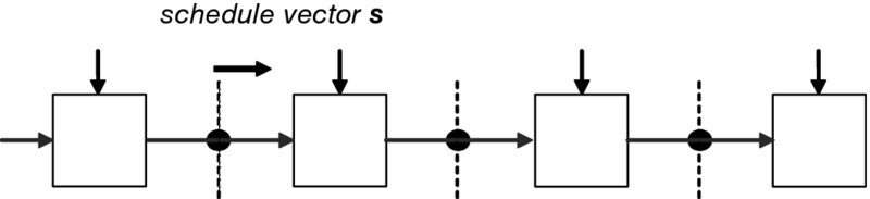
Figure 4.9 Linear systolic array
Figure 4.10 shows a classical rectangular systolic array each with local interconnections. This type of array is highly suitable for matrix–matrix operations. Each PE receives data only from its nearest neighbor and each processor contains a small memory elements in which intermediate values are stored. The control of the data through the array is by a synchronous clock, which effectively pumps the data through the array; hence the name “systolic” arrays, by analogy with the heart pumping blood around the body. Figure 4.11 depicts the systolic array applied for QR decomposition. The array is built from two types of cells, boundary and internal, all locally interconnected.
Figure 4.10 Systolic array architecture
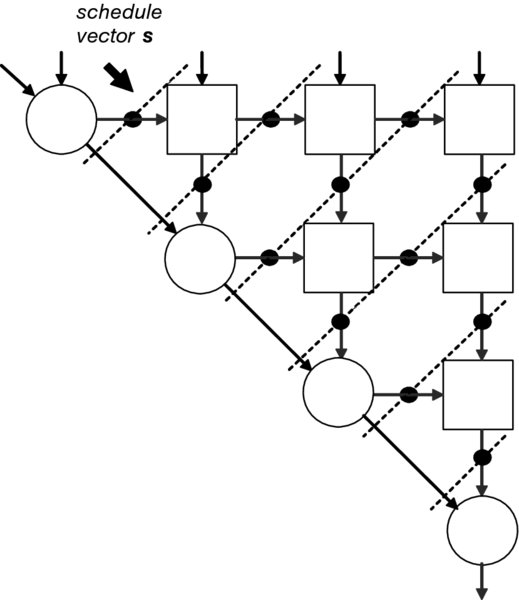
Figure 4.11 Triangular systolic array architecture
The concept of systolic arrays was employed in many DSP applications. McCanny and McWhirter (1987) applied it at the bit level, whereas the original proposer of the technique developed the concept into the iWarp which was an attempt in 1988 by Intel and Carnegie Mellon University to build an entirely parallel computing node in a single microprocessor, complete with memory and communications links (Gross and O’Hallaron 1998). The main issue with this type of development was that it was very application-specific, coping with a range of computationally complex algorithms; instead, the systolic array design concept was applied more successfully to develop a wide range of signal processing chips (Woods et al. 2008). Chapter 12 demonstrates how the concept has been successfully applied to the development of an IP core for recursive least squares filtering.
4.9 Heterogeneous Computing Platforms
Since the first edition of this book, there have been many alternative developments due to scaling issues, but rather than evolve existing platforms to cater for DSP processing, the focus has been to derive new forms of multicore platforms:
- Multicore architectures such as the Parallela (highlighted in Section 4.5.2) which offers high levels of parallelism, and coprocessing architectures such as the Intel Xeon Phi™ processor which delivers up to 2.3 times higher peak FLOPS and up to 3 times more performance per watt. The technology has been used for 3D image reconstruction in computed tomography which has primarily been accelerated using FPGAs (Hofmann et al. 2014). They show how not only parallelization can be applied but also that SIMD vectorization is critical for good performance.
- DSP/CPU processor architectures such as KeyStone™ II multicore processors, e.g. the 66AK2Hx platform which comprises a quad-ARM Cortex-A15 MPCore™ processor with up to eight TMS320C66x high-performance DSPs using the KeyStone II multicore architecture. This has been applied for cloud radio access network (RAN) stations; Flanagan (2011) shows how the platform can provide scalability.
- SoC FPGAs have evolved by incorporating processors (primarily the ARM processor) on the FPGA fabric. These effectively present a hardware/software system where the FPGA programmable fabric can be used to accelerate the data-intensive computation and the processor can be used for control and interfacing. This is discussed in more detail in the next chapter.
4.10 Conclusions
This chapter has highlighted the variety of technologies used for implementing complex DSP systems. These compare in terms of speed, power consumption and, of course, area, although this is a little difficult to ascertain for processor implementations. The chapter has taken a specific slant on programmability with regard to these technologies and, in particular, has highlighted how the underlying chip architecture can limit the performance. Indeed, the fact that it is possible to develop SoC architectures for ASIC and FPGA technologies is the key feature in achieving the high performance levels. It could be argued that the fact that FPGAs allow circuit architectures and that they are programmable are the dual factors that make them so attractive for some system implementation problems.
Whilst the aim of the chapter has been to present different technologies and, in some cases, compare and contrast them, the reality is that modem DSP systems are now collections of these different platforms. Many companies are now offering complex DSP platforms comprising CPUs, DSP processors and embedded FPGA. Thus the next chapter views FPGAs both as heterogeneous platforms in themselves but also as part of these solutions.
Bibliography
- Berkeley Design Technology 2000 Choosing a DSP processor. Available at http://www.bdti.com/MyBDTI/pubs/choose_2000.pdf (accessed November 6, 2016).
- Boland DP, Constantinides GA 2013 Word-length optimization beyond straight line code. In Proc. ACM/SIGDA Int. Symp. on Field Programmable Gate Arrays, pp. 105–114.
- Dahnoun, N 2000 Digital Signal Processing Implementation Using the TMS320C6000TM DSP Platform. Prentice Hall, Harlow.
- Falcao G, Silva V, Sousa L, Andrade J 2012 Portable LDPC decoding on multicores using OpenCL. IEEE Signal Processing Mag., 29(4), 81–109.
- Flanagan T 2011 Creating cloud base stations with TI’s KeyStone multicore architecture. Texas Instruments White Paper (accessed June 11, 2015).
- Gillan CJ 2014 On the viability of microservers for financial analytics. In Proc. IEEE Workshop on High Performance Computational Finance, pp. 29–36.
- Gross T, O’Hallaron DR 1998 iWarp: Anatomy of a Parallel Computing System. MIT Press, Cambridge, MA.
- Hofmann J, Treibig J, Hager G, Welleinet G 2014 Performance engineering for a medical imaging application on the Intel Xeon Phi accelerator. In Proc. 27th Int. Conf. on Architecture of Computing Systems, pp. 1–8.
- ITRS 2005 International Technology Roadmap for Semiconductors: Design. available from http://www.itrs.net/Links/2005ITRS/Design2005.pdf (accessed February 16, 2016).
- International Technology Roadmap for Silicon 2011 Semiconductor Industry Association. Available at http://www.itrs.net/ (accessed June 11, 2015).
- Jackson LB 1970 Roundoff noise analysis for fixed-point digital filters realized in cascade or parallel form. IEEE Trans. Audio Electroacoustics 18, 107–122.
- Kung HT, Leiserson CE 1979 Systolic arrays (for VLSI). In Proc. on Sparse Matrix, pp. 256–282.
- Kung SY 1988 VLSI Array Processors. Prentice Hall, Englewood Cliffs, NJ.
- Luo L, Wong M, Hwu W-M 2010 An effective GPU implementation of breadth-first search. In Proc. Design Automation Conf., Anaheim, CA, pp. 52–55.
- McCanny J, McWhirter JG. 1987 Some systolic array developments in the UK. IEEE Computer, 20(7), 51–63.
- Reinders J, Jeffers J 2014 High Performance Parallelism Pearls: Multicore and Many-Core Programming Approaches. Morgan Kaufmann, Waltham, MA.
- Sutter H 2009 The free lunch is over: A fundamental turn toward concurrency in software. Available at http://www.gotw.ca/publications/concurrency-ddj.htm (accessed June 11, 2015).
- Wang G, Wu M, Yang S, Cavallaro JR 2011 A massively parallel implementation of QC-LDPC decoder on GPU. In Proc. IEEE 9th Symp. on Application Specific Processors, pp. 82–85.
- Woods RF, McCanny JV, McWhirter JG. 2008 From bit level systolic arrays to HDTV processor chips. J. of VLSI Signal Processing 53(1–2), 35–49.