
Chapter 7
Leakage Currents in PZT
Capacitors 1
7.1. Introduction
Many models have been proposed in the literature in recent years to describe the conduction mechanisms of leakage current in ferroelectric thin films. For the same material PZT, it is possible to find models based on a conduction limited by the interfaces such as Schottky injection [CHE 94a, SUD 94, WOU 95a], or tunneling [KUR 01], as well as some mechanisms limited by the bulk of film like Poole-Frenkel emission [ALS 96, CHE 98, MIH 95], or space-charge limited conduction [HUH 94, SCO 94]. The wide variety of results available in the literature comes not only from the difficulty of acquiring electrical characteristics representative of the so-called “true” leakage current material, but also from the complexity of interpretation of these characteristics.
The most common method for characterizing the leakage current conduction mode in a metal/insulator/metal structure is based on the analysis of I(V) curves obtained by applying a voltage ramp. However, in the case of capacitors made of perovskite type titanium oxides, such as PZT, the recorded current density obtained in response to the application of a constant voltage stress turns out to be characterized by very significant intensity variation over time. Thus, during the acquisition of I(V) curves, the application conditions of the voltage ramp significantly affect the measurement of current and thus the interpretation of results. Many authors point out that special attention should be paid to the development of I(V) curves’ acquisition procedures that are representative of the “true” leakage current of capacitors [SLE 94a, 94 HUH, LEE 01, SOUTH 94]. However, to our knowledge, no universal measurement methodology was adopted by the scientific community to characterize properly the leakage properties in this type of structure. It is therefore reasonable to assume that a primary cause of the very diverse results published regarding leakage current conduction in PZT material comes from the great disparity in measurement procedures.
A second major reason that could explain the heterogeneity of these results can be related to the major impact of elaboration processes on the electronic properties of PZT layers. By changing the fabrication conditions of their structures, many authors highlighted the role of the microstructure [HUH 94, HSA 00, SCO 94, WAS 90a, 95b WOU], the doping [ALS 96, HOF 97, WAS 90a, 95a WOU], and the nature of the electrodes [SLE 94a, OF 99, 02 KIM, SCO 94] on the behavior of the leakage current. The conduction mechanisms seem, therefore, to be strongly dependent on process and preparation conditions. This fact increases the difficulty of comparing the results published by different research teams. In addition, some different conduction modes can result in very similar electrical characteristics. Hence, it is often necessary to conduct a comprehensive study on a wide voltage and temperature range before drawing any final conclusion about the nature of conduction mechanism.
This chapter does not propose an exhaustive description of the conduction modes encountered in all piezoelectric or ferroelectric materials, but it provides a general methodology that is especially developed for PZT structures as an application example. These PZT capacitors are obtained by sol-gel processing up to a thickness of 240 nm.
A very general description of main leakage current conduction mechanisms in metal/insulator/metal structures is presented in the first section.
The second section focuses on the problem of leakage current measurement and highlights the difficulty in acquiring I(V) characteristics representative of the real conduction mode.
The third section is devoted to the characterization and the modeling of the relaxation current that is superimposed on the true leakage current which, in turn, is likely to hide the measurement of true leakage current.
The following sections are exclusively dedicated to the characterization of the true leakage current, the first being the state-of-the-art account available in the fourth section to present the main models applied for PZT material in the literature.
In the fifth section, a dynamic model is set up to reflect the strong evolutions of the current over time, characterized especially by the phenomena of resistance degradation and restoration. This dynamic model, developed exclusively from the I(t) characteristics obtained at different voltage and temperature levels, is then validated by a static approach based on the analysis of I(V) curves. The description of this static model is the subject of the sixth section.
7.2. Leakage current in metal/insulator/metal structures
Before presenting and interpreting the electrical characterization results, we describe the traditional mechanisms of leakage current conduction in metal/insulator/metal structures and we also recall some notions specific to the metal/insulator contact.
7.2.1. Metal/insulator contact: definitions
7.2.1.1. Fermi level, work function, and electron affinity
In a crystal, electrons are located in energy levels separated by band gaps. For T = 0 K, all levels that are below the Fermi level EF are filled. By denoting as fn(E) the probability that a given energy level E is not empty, we have:

When the temperature increases, for T > 0 K, the electronic distribution loses its “binary” nature. The probability that the energy level E is not empty is determined by Fermi-Dirac statistics:

In the case of metals, the Fermi level EF lies inside the conduction band. The work function of the metal ΦM represents the energy required to extract an electron from the conduction band toward the vacuum level. The vacuum level is defined as the reference energy possessed by a single electron isolated in the vacuum.
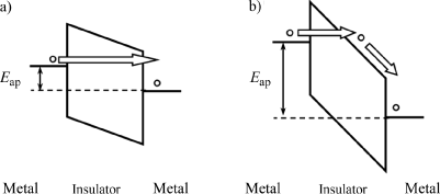
For an insulator or a semiconductor, the Fermi level EF lies in the band gap. The energy required to bring an electron from the conduction band toward the vacuum level in this case is represented by the electron affinity χ. The work function ΦS required to extract an electron from the Fermi level toward the vacuum level is then χ + ξ, with ξ defined by the difference EC−EF, as shown schematically in Figure 7.1.
Figure 7.1. Metal/insulator out of contact energy diagram

When a metal and an insulator, or a semiconductor, come into contact once the thermodynamic equilibrium is reached, the Fermi levels of the two materials are aligned. The bands’ structure near the interface is then conditioned by the possible difference in work functions of both materials.
7.2.1.2. Neutral contact
If the work functions are equivalent, i.e. ΦM = ΦS, the alignment of the Fermi levels does not require any band curvature in the insulator, as shown in Figure 7.2. The barrier height at the interface is, therefore, Φ0 = ΦM−χ = ξ. This barrier height represents the energy needed by an electron to move from the Fermi level of the metal toward the conduction band of the insulator.
Figure 7.2. Energy diagram of a neutral metal/insulator contact

7.2.1.3. Blocking contact
Figure 7.3. Energy band diagram of a blocking metal/insulator contact

If ΦM>χ + ξ, in the case of an insulator or a n-type semiconductor, the alignment of the Fermi levels leads to an upward band curvature as shown in Figure 7.3.
In fact because the work function of the metal is greater than the work function of the insulator the flow of electrons from the insulator to the metal leads to the creation of a depletion layer and the appearance of a positive space charge area.
In any metal, to ensure the electric neutrality of the structure, an accumulation of electrons appears at the interface. The obtained energy contact in this case is called “blocking” contact since the flow of the carriers from the metal to the insulator is conditioned by the contribution of a certain amount of energy determined by the barrier height Φ = ΦM−χ. The blocking contact is also observed when ΦM< χ + ξ in the case of a p -type semiconductor [BAR 86].
7.2.1.4. Ohmic contact
If ΦM<χ + ξ in the case of an insulator or a n-type semiconductor the alignment of the Fermi levels leads to a downward band curvature as shown in Figure 7.4
Figure 7.4. Energy band diagram of an ohmic metal/insulator contact

In fact, because the metal work function in this case is lower than the insulator work function, the electrons leave the metal to enter the insulator. An accumulation layer of electrons is formed at the interface of the insulator, while a depletion layer appears in the metal. When the accumulation width reaches a size close to the thickness of the insulator, the electron density highly exceeds the intrinsic density of the carriers. The result is a perfect injection at the interface and the current is therefore only limited by the bulk material. This type of contact called “ohmic” also occurs when ΦM > χ + ξ in the case of an insulator or a p-type semiconductor [BAR 86].
7.2.1.5. Intrinsic and extrinsic carriers
The carriers are called “intrinsic” when they come from the insulating material itself and “extrinsic” when they are injected by the electrodes. After a certain voltage threshold, the conduction is ensured by the extrinsic carriers and the transport mechanisms can be divided into two main categories:
- either the carriers’ injection is limited by the interfaces and the injected electrons move freely through the film (Schottky emission, tunneling conduction);
- either the electrodes act as infinite sources of carriers and the current is limited by the bulk of the film (Poole-Frenkel effect, carriers hopping conduction from trap to trap, current limited by the space charge).
7.2.2. Conduction mechanisms limited by the interfaces
The conduction mechanisms limited by the interfaces are observed when the metal/insulator contact is of the neutral or blocking type.
7.2.2.1. Schottky emission
In the case of Schottky emission, or thermoionic emission, the current is generated by the flow of the carriers that transit over the potential barrier at the interface (Figure 7.5). By denoting Φm as the energy barrier height to overcome by the carriers, the expression of the thermoionic current is given by equation [7.1]:
[7.1] ![]()
A* denotes the Richardson constant modified by the introduction of m*, the electron’s effective mass, which replaces the free electrons’ mass m0:
[7.2] ![]()
The term Φm corresponds to the maximum of the potential energy curve of the injected carriers Φ(x). This evolution of potential energy in the film thickness is described by equation [7.3], in which Φ0, Φim(x), and Eext denote, respectively, the energy difference between the Fermi level of the metal and the conduction band of the insulator, the barrier lowering resulting from the image force [BAR 86], and the applied field:
[7.3] ![]()
Using the approximation of the lowering Φim(x) valid for regions close to the interface [BAR 86], we get:
[7.4] ![]()
The maximum Φm is reached for the value xm that satisfies the condition dΦ(x)/dx = 0. By substituting equation [7.4] into equation [7.3], we obtain for xm after derivation:
[7.5] ![]()
The energy barrier Φm at the metal/insulator interface is then obtained by setting x = xm in equation [7.3]:
[7.6] ![]()
The final expression giving the evolution of the thermoionic current as a function of the temperature and the applied electric field Eext is finally obtained by implementing the expression Φm in equation [7.1]:
[7.7] 
At constant temperature, the semi-logarithmic representation ln ![]() of a Schottky current is a linear characteristic curve with a slope controlled by the constant εi, defined as the square of the optical refractive index of the material: εi =n2.
of a Schottky current is a linear characteristic curve with a slope controlled by the constant εi, defined as the square of the optical refractive index of the material: εi =n2.
Figure 7.5. Energy band diagram of a metal/insulator/metal structure under the effect of an applied voltage Vext: illustration of the Schottky injection mechanism

7.2.2.2. Tunneling conduction
The tunneling conduction occurs when the carriers have an insufficient energy to get over the potential barrier at the interface. The only way for these carriers to be injected into the oxide is to cross the barrier by tunneling. The current density thus depends on the amount of electrons that could transit through tunneling, on their energy distribution given by Fermi-Dirac statistics f(E) and on the transparency T(E) that represents the probability that an electron of energy E passes through the energy barrier of the oxide [BAR 86]. Depending on the applied electric field level, there are two possibilities: the direct tunneling and the Fowler-Nordheim tunneling, shown schematically in Figures 7.6(a) and (b), respectively.
The direct tunneling configuration corresponds to a trapezoidal barrier that is observed at low electric fields. The carriers are injected in this case directly from one electrode to another without transiting in the insulator.
The Fowler-Nordheim tunneling is observed at a higher field, in the case of a triangular barrier configuration. After crossing the barrier, the carriers transit through the conduction band of the insulator before reaching the other interface. In the latter case, the simplified expression of the Fowler-Nordheim current density is written as follows [BAR 86]:
[7.8] 
Figure 7.6. (a) Illustration of the direct tunneling and (b) the Fowler-Nordheim tunneling
7.2.3. Conduction mechanisms limited by the bulk of film
In the case of an ohmic contact, the injection through the interfaces is considered as perfect and the leakage current depends only on the electronic properties of the insulator. The conduction of carriers in the insulator is then based on the trapping/detrapping mechanisms through shallow trap levels Nt and through donor levels ND located from a few tenths of electron volts to a few electron volts below the conduction band.
As long as the trap levels are not saturated, the electronic conduction is ensured by the transfer of carriers from traps to traps. Considering the energy diagram in Figure 7.7, two conduction mechanisms are possible: the Poole-Frenkel emission (thermionic effect) and the carriers hopping conduction from traps to traps (tunneling).
When the injection becomes strong, a space charge is established in the film, due to accumulation of charges in the insulator. We could now visualize a conduction regime limited by the space charge.
Figure 7.7. Potential energy diagram of an insulator containing trap levels, subject to an applied voltage Vext. The thermionic emission is responsible for the Poole-Frenkel type conduction mode while the tunneling corresponds to the carriers’ hopping conduction

7.2.3.1. Poole-Frenkel emission
Poole-Frenkel emission takes place when the carriers have enough energy to overcome the potential barrier by thermoionic emission (Ecarriers > Φm). For a given trap site, the barrier height Φm is calculated by taking into account the decrease in potential energy due to Coulomb interactions of the carriers trapped in adjacent sites. Assuming that the trapping sites are sufficiently spaced, the evolution of the energy barrier height with the applied field Eext can be approximated by equation [7.9]:
[7.9] 
In the case of a thin film for which the width of the electrons’ accumulation zone at the interface is large compared to the thickness of the film, the Poole-Frenkel current evolution is given by equation [7.10]:
[7.10] 
The general expression for the transport of charges in a material is given in this equation, with μ the carrier mobility, Eext the applied electric field, and q the elementary charge. The following term represents the density of carriers coming from the trap levels and transiting through the conduction band.

7.2.3.2. Hopping conduction
When the energy of the carriers is too low to overcome the potential barrier (Ecarriers < Φm), the conduction can be achieved by tunneling. This is the carriers’ hopping conduction from traps to traps, more commonly known as hopping. The current is then directly proportional to the applied field, and also depends on the density of trapped electrons and on the hops’ frequency between two sites. A simplified mathematical expression of the current density obtained by this mechanism is given by equation [7.11]:
[7.11] ![]()
τ0 is a time constant, a denotes the distance between two traps, and n* is the density of the trapped carriers.
7.2.3.3. Conduction limited by the space charge
In both the mechanisms of Poole-Frenkel emission and hopping, the electric field is assumed to be constant considering the thickness of the insulator. This assumption becomes invalid when the injection of carriers becomes too high because of the space charge established in the film. The potential distribution is then modified according to Poisson’s law and evolution of the current density limited by the space charge is given by equation [7.12]:
[7.12] ![]()
θ denotes the traps’ filling ratio, μ is the electron mobility of the carriers, d is the film thickness, and Vext is the applied voltage.
The so-called “very high injection” system is reached when all the traps are filled (θ = 1). The threshold voltage of trap-filled limit characterizes the transition between high and very high injection regimes:
![]()
where Nt denotes the trap’s density.
7.3. Problem of leakage current measurement
The most direct approach to characterize the conduction mode of leakage current in a metal/insulator/metal structure is to analyze the I(V) curves obtained at a given temperature.
In fact, each conduction mechanism is characterized by a specific law that governs the evolution of leakage current as a function of the voltage and the temperature I (V, T). As a result, the acquisition of I(V) characteristics should theoretically enable us to determine with certainty the conduction mechanism nature associated with a given structure, by comparing the experimental data with the theoretical conduction models.
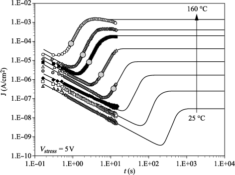
However, none of the models presented in the previous section takes into account the time dependence of the leakage current. This time dependence is illustrated by the I(t) curves’ network in Figure 7.8, in which I(t) characteristics were recorded in response to the application of a constant voltage of 5 V, for temperatures ranging from 25°C to 220°C. At low temperatures, the presence of relaxation currents leads to a continuous decrease in current density over time. Several decades of time are then required to reach the stability of the measurement, and to extract the values of true leakage current. Conversely, when the temperature increases, large deviations of the true leakage current appear. These are the phenomena of resistance “degradation” and “restoration”.
In this section, we propose to tackle the problem of true leakage current extraction by describing the experimental procedures of I(V) characteristics acquisition, before illustrating the limitations of these experimental procedures and presenting the characterization strategy adopted for the rest of the study. The leakage current measurements are performed using a 236 Keithley voltage/current source measure unit, coupled with a cascade probing station.
Figure 7.8. Time evolution of leakage current of a capacitor under 5 V, from 25°C to 220°C, in positive polarity applied to the top electrode

7.3.1. Relaxation current and true leakage current
Many authors emphasize the necessity to establish acquisition procedures of I(V) curves that ensure the elimination of the relaxation currents that are superimposed on the true leakage current of the capacitors [CHE 93, CHE 98, DIE 95, HUH 94, LEE 01, STO 00, WAS 92, WOU 65b].
The most common measurement procedures are the acquisitions in “staircase” mode and in “pulse” mode, explained schematically in Figures 7.9(a) and (b), respectively.
Figure 7.9. Voltage ramp in staircase mode (a) and in pulse mode (b)

7.3.1.1. Staircase procedure
The staircase procedure consists of the application of a linear staircase voltage ramp, by imposing a fixed voltage scan step ΔV, and a fixed staircase duration Δt. The I(V) characteristics are then obtained by representing the current values measured at the end of each voltage stair. The time evolution of leakage current on each stair includes a relaxation component that is superimposed on the true leakage current of the capacitor: I(t) = Irelax(t) + Itrue. If the staircase duration is long enough, the I(t) characteristics reach a saturation value, and the relaxation current thus becomes negligible compared to the true leakage current.
To verify that the I(V) curves obtained at the end of the acquisition are representative of the evolution of the true leakage current, we just need to ensure the saturation of the I(t) characteristics at the end of each voltage step.
The impact of the relaxation current on the representation of I(V) curves is illustrated in Figures 7.10 and 7.11. The characteristics S1, S10, and S100 were obtained by an acquisition in staircase mode by applying voltage stairs of 1, 10, and 100 s. At low voltage levels (V < 4 V), the significant gap between the characteristics S1, S10, and S100 reflects the presence of strong relaxation currents.
The superposition of three characteristics from 4 V indicates that from this voltage level, the relaxation current becomes almost instantly negligible compared to the true leakage current.
This transition is also visible on the I(t) characteristics in Figure 7.11. The current decay turns out to be pretty high at low voltages, to be gradually replaced by more stable characteristics from 4 V.
Figure 7.10. Illustration of the impact of relaxation currents on the shape of the I(V) characteristics, obtained at 85°C in staircase mode with staircase time switching of 1 s (S1), 10 s (S10), and 100 s (S100)

Figure 7.11. I(t) curves measured for voltage stairs from 1 to 10 V during the S100 staircase procedure at 85°C

Figures 7.10 and 7.11 clearly illustrate the influence of relaxation currents on the shape of I(V) characteristics obtained in the staircase mode. The evolution of the measurement results, depending on the applied experimental conditions, demonstrates the need for staircase duration to be long enough to reach saturation values that are representative of the true leakage current level. However, for low voltage and temperature stresses the relaxation currents are often largely predominant, so that stress durations of several hours may be needed to reach the true leakage current at room temperature. Hence, the first limitation of the staircase procedure is signified by these prohibitive characterization durations. Some authors such as Wouters et al. [WOU 95b] rather prefer to restrict their studies to temperatures above 100°C for which the relaxation current quickly becomes negligible.
7.3.1.2. Pulse procedure
The acquisition process by variable pulses amplitude, more simply called the “pulse” mode, is a procedure often recommended for its ability to separate the relaxation and true leakage current contributions [CHE 98, LEE 01, STO 00]. The pulse procedure consists of the application of successive levels of voltage separated by short-circuit intervals, as shown schematically in Figure 7.9b. The I(t) characteristics of charge and discharge are then collected during the polarization and short-circuit phases, respectively. According to Dietz and Waser [DIE 95], the relaxation current can be attributed to the displacement of the charges stored in the capacitor, while the true leakage current reflects the real flow of charges between the electrodes.
During the discharge phases, a current equivalent to the relaxation current is recorded up to a sign. Thus, a simple subtraction between the charge and discharge currents leads to the evaluation of true leakage current:
[7.13] ![]()
Figure 7.12 shows the charge and discharge I(V) curves obtained in pulse mode at 85°C, imposing the staircase duration of 100 s. The discharge current quickly reaches a saturation value in I(V) representation, which explains that above a few volts, the relaxation current quickly becomes negligible compared to the true leakage current. The charge and discharge I(t) characteristics shown in Figure 7.13 illustrate the intrinsic decreasing nature of the discharge current (relaxation phenomenon), while the charge current tends to stabilize around the true leakage current value.
Figure 7.12. Charge and discharge I(V) curves measured in pulse mode by steps of 0.2 V at the end of 100 s steps. T = 85°C

Figure 7.13. Charge and discharge I(t) curves for a voltage level of 4 V. T = 85°C
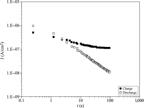
The I(V) characteristics obtained after extraction of the true leakage current in pulse mode, on the one hand, and by simple acquisition in staircase mode, on the other, are superimposed in Figure 7.14. The consistency of the results obtained by these two procedures indicates that at 85°C, steps of 100 s of duration enable us to obtain I(V) curves representative of the true leakage current. However, the application of the pulse or staircase procedures for temperatures above 85°C remains problematic, because the current measured at such temperatures undergoes a rapid degradation phenomenon, as shown in Figure 7.8, which raises the problem of true leakage current drift.
7.3.2. Drift of true leakage current
When the temperature rises above 125°C, the relaxation currents become quickly negligible compared to the true leakage current, even at low voltages. This fact is confirmed in Figure 7.15, by the superposition of the I(V) characteristics measured in staircase mode, applying 10 and 100 s duration voltage steps, below 1.6 V.
Figure 7.14. I(V) curves obtained in pulsed mode and in staircase mode, by subtraction of the charge and discharge currents. The current is measured at the end of 100 s stages, by steps of 0.2 V. T = 85°C

Figure 7.15. I(V) curves at 125°C in staircase mode with respective staircase step duration of 10 s (S10) and 100 s (S100)

Figure 7.16. I(t) curves at 125°C measured from 1 to 10 V during the S100 staircase procedure

The difference between the S10 and S100 characteristics beyond 1.6 V highlights the problem of drift of true leakage current. In fact, in Figure 7.16, we observe a gradual increase in leakage current under 2 V, during the acquisition of the S100 characteristic. This instability vanishes for voltage levels up to 3 V that marks the end of the degradation mechanism. This degradation is also involved in the acquisition of the S10 characteristic, but its process in this case is naturally more spread out in the voltage range, since the stress sustained by the capacitor at each voltage level is 10 times shorter. Beyond 7 V, the S10 and S100 characteristics are superimposed again, indicating the end of the degradation mechanisms for S10.
7.3.3. Discussion
The determination of leakage current conduction mode in metal/insulator/metal structures necessitates the acquisition of I(V) characteristics representative of the true leakage current, over a wide voltage and temperature range. In the case of PZT capacitors, the obtention of these I(V) characteristics raises many difficulties. When the voltage and/or temperature stresses are low, the predominance of relaxation currents requires the application of voltage stairs long enough to reach saturation values. In contrast, when the voltage and temperature levels increase, the application of much lengthy stairs is followed by a deterioration of the true leakage current. To address this problem, Hu and Krupanidhi [HUH 94] proposed an original experimental procedure that associates long stairs with lowest voltages and short stairs with highest voltages. However, the determination of the transition voltage as well as the stair length required for each temperature level remains difficult to define and largely empirical.
In this section, we have illustrated the experimental complexity of acquiring I(V) curves representative of the leakage current conduction mode in PZT structures. Moreover, this section highlights the limitations of the traditional procedures generally adopted for leakage current acquisition, especially regarding the resistance degradation problem. The determination of a reliable methodology for the acquisition of I(V) curves, valid over a wide voltage and temperature range, requires a thorough study of the phenomena governing the time evolution of the leakage current. Therefore, we propose for any advanced study of leakage current to adopt the following characterization strategy:
– model the relaxation currents Jrelax(t,V,T) from I(t) characteristics obtained by applying low voltage and temperature stresses, to quantify the contribution of relaxation currents at any given voltage and temperature level;
– characterize the time-dependent phenomena of resistance degradation and restoration based on the analysis of I(t) curves measured from high voltage and/or temperature stresses, and thus model the dynamic evolution of the true leakage current Jtrue(t, V, T);
– establish an experimental procedure to achieve a quasi-steady state of leakage current, such as the maximal level of current Jmax observed after degradation, and model through a more conventional static approach the current Jmax(V, T); and
– check the consistency of the model by comparing the results obtained by the static and dynamic approaches.
7.4. Characterization of the relaxation current
7.4.1. Origin of the relaxation current
In this section, we focus on the relaxation phenomenon responsible for the initial decrease in time evolution of leakage current, in response to the application of a constant voltage. This phenomenon is particularly visible at low temperatures, as shown in Figure 7.8.
When a constant voltage is applied across a ferroelectric material, the current response is primarily characterized by a peak caused by the reversal of ferroelectric domains, followed by an exponential decay due to the charge in the measurement circuit. The reversal kinetics of the ferroelectric domains is generally less than 100 ns [CHE 93], while the time constant characterizing the charge of the measurement circuit is about 1 ms. These two phenomena can therefore in no way be responsible for the relaxation that often spreads over several decades of time.
The relaxation currents are generally described by the universal Curie–Von Schweidler law [HOF 97, STO 00], given by equation [7.14]. According to this law, current can be decomposed into two components: one component representing the true leakage current Jtrue and a relaxation component Jrelax that evolves according to a decreasing power law:
[7.14] ![]()
The main mechanisms proposed in the literature to justify the origin of the relaxation currents are described by the “distribution of interfacial polarization mechanisms” [WAS 92], “N-body interaction” [CHE 93, 83 JON, WAS 92], and “space charge relaxation” [SCO 93] models. These models adequately describe the mechanisms of emergence of relaxation currents. It is thus probable that the relaxation currents have various origins and that these phenomena can occur simultaneously.
7.4.2. Modeling of relaxation currents
For a complete modeling of relaxation currents, it is necessary to describe the evolution of the parameters n and JO as a function of temperature and voltage.
7.4.2.1. Temperature evolution
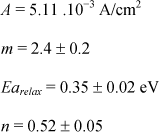
The modeling of relaxation current as a function of temperature is shown in Figure 7.17. The fit of experimental data, obtained for a voltage of 5 V, from 25°C to 105°C, is performed only on the portion of current decay. The phenomenon of resistance degradation, which appears starting from 85°C, is not taken into account in the modeling process. The factor n seems to be independent of the temperature: n = 0.52 ± 0.05; while the term J0 is thermally activated as shown in the Arrhenius graph of Figure 7.18:
![]()
Figure 7.17. Experimental and simulated results of relaxation current at 5 V, from 30°C to 105°C, in positive polarity applied to the top electrode (+/TE)

Figure 7.18. Temperature evolution in the relaxation term JO = A.exp(Earelax/kT), Earelax = 0.35 eV

7.4.2.2. Voltage evolution
The experimental and simulated results of relaxation current as a function of the applied voltage stress are shown in Figure 7.19. The adjustment of the experimental measurements obtained at 30°C, from 5 V to 14 V, is performed only on the portion of the current power law decay.
The stabilization toward a true leakage current level observed on the characteristic at 14 V is not taken into account in the modeling process. The factor n of the model Jrelax=J0.t−n seems to be independent of voltage level. We find again the value of 0.52 has been previously obtained in the literature.
According to the logarithmic representation in Figure 7.20, the interpolation of the J0 term by a power law turns out to be well adapted: J0 = A·Vm. The factor m is estimated at 2.4 ±0.2.
Figure 7.19. Experimental and simulated results of relaxation currents at 30°C, 5 to 14 V, in positive polarity applied to the top electrode

Figure 7.20. Voltage evolution of the relaxation term JO = A.Vm, m = 2.42 ±0.2

7.4.3. Conclusion
The relaxation current behavioral modeling process can be performed using the analysis of I(t) characteristics obtained at different voltage and temperature levels. This characterization step is essential for the analysis of the true leakage current that can be obtained after subtracting the relaxation component.
The complete model describing the temporal evolution of the relaxation current as a function of voltage and temperature stresses is described by equation [7.15]:
[7.15] ![]()
Relaxation parameters in positive polarity applied to the top electrode include:
7.5. Literature review of true leakage current in PZT
After some time, under constant voltage stress, the leakage current of PZT capacitors reaches a first saturation regime: the true leakage current becomes dominant compared to the relaxation current. This section and the next are devoted to the study of the conduction mode of the true leakage current. In other words, we focus on the electronic mechanisms responsible for the charges’ injection and transport in the PZT.
As emphasized by Chen and Kingon [SLE 94a], the results published before the 1990s on the conduction of the leakage current in structures based on ferroelectric materials such as PZT are generally not followed by detailed descriptions of the true leakage current acquisition procedures. Because the interpretation of the I(V) characteristics in this case is likely to be disturbed by the presence of relaxation currents, the results obtained prior to 1990 are not taken into consideration in our study.
In 1990, Moazzami et al. [MOA 90] attribute, as a first step, the origin of the leakage current in PZT structures to an ionic transport, namely a conduction mechanism limited by the bulk. The same authors showed four years later [SOU 94] the role of the interfaces and suggested a model of double injection of carriers through blocking contacts (Schottky), with a space-charge-limited current (SCLC) for the high-injection regimes.
In 1994, Kingon’s group [SLE 94a] observed an ohmic behavior at low voltages, followed by a Schottky regime at higher voltages, while Hu and Krupanidhi [HUH 94] described a conduction that can be limited either by the space charge (SCLC) or by the grain boundaries (grain boundary limited current) depending on the microstructure of PZT films. The same year, Scott’s group compared the conduction modes in structures based on PZT and BST [SCO 94].
For BST, Scott mentions some conduction modes limited by the interfaces, with successive regimes of tunneling and Schottky emission. The Schottky emission for BST was confirmed by Waser in 1997 [WAS 97] and Kotecki et al. in 1999 [KOT 99]. For PZT, however, the leakage current behavior observed by Scott is characteristic of a conduction limited by the space charge (SCLC). This conduction mode is consistent with the microstructure of columnar grains that allows us to create high space charge currents.
In 1995, Mihara and Watanabe [MIH 95] suggested for PZT a more complex model combining Schottky and Poole–Frenkel emissions. Further, in 1995, Wouters [WOU 95b] considered all the models proposed in the literature and made an attempt to establish a detailed description of the energy band diagram of the Pt/PZT/Pt structures. According to this analysis, the PZT would be completely depleted from free carriers and the conduction would be ensured by the injection of holes, but no final conclusion is drawn regarding the conduction mode. Other results reported by Wouters et al. [WOU 95a] the same year seem to favor the mechanism of Schottky emission.
According to the two articles written in 1996 and 1998 by Al-Shareef and Dimos on the one hand [ALS 96], and by Chen et al. on the other [CHE 98], it is the Poole– Frenkel model that is considered the most suitable model. The hypothesis of lead vacancies as a possible center for trapping holes is proposed by Al-Shareef and Dimos. The corresponding trap depths are estimated at 1.3 eV from the valence band. These centers were already mentioned by Mihara and Watanabe [MIH 95] to support a possible Poole-Frenkel emission mechanism, but the reported trap depths were of the order of 0.5 eV.
More recently, Kurasawa et al. [KUR 01], Shye et al. [DSH 03], Lee et al. [LEE 01], Boaresu et al. [BOE 03], Baniecki et al. [BAN 03], and Masuda and Nozaka [MAS 04] proposed some comprehensive analyses of the conduction mechanisms in their structures. The interpretations are very diverse, from the description of the classical Schottky mechanisms [BOE 03, LEE 01] to the combination of Schottky emission and tunneling injection [03 DSH, KUR 01], through the combination of Schottky emission and SCLC [MAS 04].
From 1998, Stolichnov and Tagantsev [STO 98a, STO 98b, STO 98c] have developed a model of space-charge influenced injection in a series of articles. This very comprehensive model allows the description of the leakage current over a wide range of voltages and temperatures, and fits relatively well to our results, as discussed in the last section.
However, this purely static model does not take into account the time dependence of the true leakage current. The amplitude of current density variation over time is very important in our structures, as illustrated by the I(t) curves’ networks in Figures 7.21 and 7.22. Hence, before considering any static electrical characterization through the I(V) curves, we believe that it is appropriate to conduct a thorough study of the dynamic phenomena of resistance degradation and resistance restoration that govern the time evolution of true leakage current.
7.6. Dynamic characterization of true leakage current: I(t,T)
In the case of asymmetric structures in terms of electrode materials, such as IrO2/PZT/Pt stacks, the comparison of the I(V) and/or I(t) characteristics as a function of the applied polarity allows us to make some assumptions about the leakage current conduction mode. Figures 7.23 and 7.24 show the evolution of I(t) characteristics recorded at temperatures ranging from 25 to 240°C under a constant voltage of 5 V, by applying positive and negative polarities, on the top electrode (IrO2). The asymmetry of the I(t) characteristics, depending on the applied polarity, favors the hypothesis of a conduction mechanism limited by the interfaces, at the expense of a purely bulk mechanism for which the nature of the electrodes should not have any influence on the carriers’ injection.
In addition, in the family of conduction mechanisms limited by the interfaces, only Schottky emission can explain the strong thermal activation observed. Indeed, conduction by tunneling is virtually independent of temperature.
Furthermore, the time evolution of the leakage current is characterized by the successive phenomena of “resistance degradation” and then “resistance restoration”. These dynamic phenomena observed under constant stresses can be interpreted as the result of a change in the parameters of carriers’ injection over time. Schottky emission mechanism is mainly governed by the heights of energy barrier at metal/insulator contacts. It can then be assumed that the phenomena of resistance degradation and restoration result from an alteration of these barrier heights under the effect of the applied electric field.
In this section, we focus on the modeling of resistance degradation and restoration phenomena that govern the time evolution of true leakage current, and attempt to throw light on the physical origin of these phenomena.
Figure 7.21. Temperature evolution of I(t) characteristics. Vstress = 5 V, T = 25−220°C, polarity +/TE

Figure 7.22. Temperature evolution of I(t) characteristics. Vstress = 5 V, T = 25−220°C, polarity −/TE

7.6.1. Study of the resistance degradation
7.6.1.1. State of the art
Resistance degradation is a phenomenon observed especially in capacitors using ceramic materials of titanium oxide type dielectric, structured according to a perovskite network. This phenomenon results in a slow and gradual increase in leakage current under the effect of a constant voltage and temperature stress. For memory applications, such as DRAM [CHE 94b, ZAF 99, ZUR 99], this increase in leakage current, which can reach several decades, is considered as a failure mode. However, contrary to breakdown phenomenon effect, resistance degradation does not alter the dielectric properties of films. Thus, in the case of decoupling or filtering capacitor applications, the resistance degradation should not be considered as a real failure mode.
The first publications dealing with the problem of resistance degradation involved BaTiO3-type ceramics in the early 1950s [BUN 51]. According to the literature reviews by Waser et al. [WAS 90a], and then by Yoo and Desu [DES 93], different physical models were proposed before the 1990s to explain the origin of resistance degradation. These models can be classified into three categories. The first model’s family is based on the apparition of strong electric fields localized at the grain boundaries. These strong electric fields can lead to either localized dielectric breakdowns or the emission of carriers through Poole-Frenkel effect, which in both cases could justify the increase in the leakage current level.
The second model to which most authors adhere is the reduction model. This model is based on the mobility of oxygen vacancies. The oxygen vacancies constitute a major crystalline defect for materials of titanium oxides. The mobility of these vacancies was particularly highlighted in BaTiO3 material by Schaffrin in 1976 [SCH 76]. In the reduction model, the oxygen vacancies, being positively charged, are supposed to migrate toward the cathode under the effect of an applied electric field. The interface with the cathode thus becomes a zone of accumulation of oxygen vacancies, which can result in a chemical reduction of the material. This accumulation of vacancies at the cathode would be compensated by the injection of electrons, causing a large increase in electronic conductivity. In return, the oxygen diffusion toward the anode is followed by oxidation reactions that result in the formation of gaseous oxygen and the release of the conduction electrons.
A third model, still based on the diffusion of oxygen vacancies, suggests that the origin of the degradation would come from the creation of a p–n junction within the dielectric. Actually, the migration of oxygen vacancies would create a vacancies’ concentration ramp through the thickness of the film: a n-type zone is created near the cathode, while a p-type region is established near the anode. The direct polarization of this p–n junction would explain the basis for the increase in current.
In the early 1990s, Waser [BAI 90] and Desu [OF 93] considered, based on a number of experimental observations, that the third model is the most qualified to explain the origin of the resistance degradation. The main experimental results in this regard are described below.
7.6.1.1.1. Role of oxygen vacancies
By combining electrical characterizations and electrocoloration experiments, Waser [WAS 90b] first demonstrated the essential role of oxygen vacancies in the degradation process of Fe-doped SrTiO3 samples. When subjected to a constant electric field, a bright color front moving toward the cathode appears on these samples initially red, while a darker color appears at the anode. The major result highlighted by Waser is that the speed of the color front displacement is perfectly correlated with the kinetics of resistance degradation apparition. This result indicates that the degradation phenomenon is connected to a displacement of mobile species. Besides, based on thermodynamic considerations, many studies on the structural defects of perovskite type titanium oxides have shown that oxygen vacancies were the only mobile species in the range of temperatures at which the resistance degradation is observed [CHA 76, SEU 74, WAL 67]. Thus, Waser attributes the electrocoloration of its samples to an electrochemical equilibrium between Fe3+ and Fe4+ controlled by the migration of oxygen vacancies. The bright front is a vacancy-rich area where Fe4+ ions are reduced to Fe3+, which explains the loss of coloration. At the anode, the disappearance of oxygen vacancies causes the oxidation of Fe3+ to Fe4+, leading to the appearance of the darker color.
On the other hand, Waser looked at the influence of SrTiO3 films doping on the resistance degradation. First of all, he found that the La3+ lanthanum doping, which just replaces the Sr2+ and acts as a donor element, eliminates the resistance degradation. Conversely, the Mn3+ doping, which acts as an acceptor center when it is substituted with Ti4+, results in an acceleration of the degradation [WAS 90a]. Hence, Waser links the nature of the doping to the concentration of oxygen vacancies on the basis of the following electrochemical equilibria:
[7.16a] ![]()
[7.16b] ![]()
[7.16c] ![]()
[7.16d] ![]()
[7.16e] ![]()
where:
– Ml− denotes the monovalent acceptors such as Mn3+ ions on ![]() sites;
sites;
– Mh+ denotes the monovalent donors such as La3+ ions on Sr ![]() sites;
sites;
– ![]() and
and ![]() denote, respectively, the strontium and oxygen vacancies.
denote, respectively, the strontium and oxygen vacancies.
According to the electroneutrality condition described by equation [7.17], the doping in donor elements Mh+ is followed by a decrease in the concentration of oxygen vacancies, while the doping in Ml− acceptors increases the number of vacancies. The parameters n and p represent the concentration of electrons e and holes h, respectively:
[7.17] ![]()
Thus, the disappearance of the degradation caused by the lanthanum doping can be correlated with a decrease in the concentration of oxygen vacancies, while the amplification of the degradation observed in the case of Mn doping is due to the excess of vacancies generated.
In addition, the microstructure of the films plays a major role on the kinetics of degradation. The smaller the grain’s size is, the later is the appearance of the resistance degradation [WAS 90a]. Thus, it is reasonable to expect that the grain boundaries form energy barriers that slow down the migration of oxygen vacancies. This interpretation is consistent with Schaffrin’s results [SCH 76] that demonstrate that the conductivity is much lower in grain boundaries than in the bulk of grains. Thus, it would effectively be the grain boundaries that limit the diffusion of oxygen vacancies.
In 1993, Scott et al. [SCO 94] described the phenomenon of resistance degradation in PZT and BST thin films. For PZT films, which exhibit a columnar microstructure, the authors adhered to the model proposed by Waser, that is, the creation of a p–n junction induced by an oxygen vacancies’ ramp. On the contrary, for BST material, Scott emphasizes the very fine grain size of their films. Such a microstructure prevents the migration of oxygen vacancies. This is the reason why they prefer an interpretation based on the model of multiple breakdowns at the grain boundaries proposed by Arlt and Neumann [NEU 86].
7.6.1.1.2. Role of the interfaces
In 1994, Kingon’s team [SLE 94b] found that the resistance degradation observed in PZT samples was strongly dependent on the ambient humidity, as well as the polarity orientation. As a result, Kingon et al. proposed an interpretation of the degradation based on electrochemical reactions between PZT and water molecules at the interfaces.
In 1995, Wouters et al. [WOU 95b] emphasized the role of oxygen vacancies in the degradation process as demonstrated by Waser [90 BAI, WAS 90a, 90b WAS]. However, they refute the hypothesis of an increase in conductivity related to the direct polarization of a p–n junction formed by the ramp of vacancies’ concentration. Their main argument is based on the depletion of the free carriers in the film when an electric field is applied. It is indeed understood that the electrons and holes can be easily swept away by the field in the n and p regions so that the electronic conductivity of the film cannot be influenced by the presence of these two regions.
According to Wouters, the increase in leakage current density should be attributed to an interface effect: the redistribution of oxygen vacancies would lead to a change in bands’ curvature at the metal/PZT contact. This change of bands’ curvature results in a lowering of energy barrier height, leading to an increase in carriers’ injection. However, the quantitative description of the mechanism of energy barrier lowering at the interfaces is not detailed by Wouters.
7.6.1.2. Modeling of the resistance degradation
In 1999, the qualitative model of band structure modification at the interfaces proposed by Wouters [WOU 95b] was adopted by Zafar et al. [ZAF 99], and also by Zurcher et al. [ZUR 99] to explain the resistance degradation in BST samples. Zafar et al. also proposed a quantitative description of this barrier-lowering effect. This model assumes that the conduction is related to a Schottky injection of electrons at the BST/cathode interface. The time dependence of barrier lowering δΦ1, caused by the accumulation of vacancies at the cathode, is given by equation [7.18]:
[7.18] 
The term δΦmax1 denotes the maximum barrier height lowering, τ1 is the characteristic time constant for which the barrier-lowering process reaches 63% of its maximum value, and β1 is a fit parameter representative of the degradation slope.
By considering a classic Schottky injection as the conduction mode, the evolution of the current density corrected by the barrier lowering δΦ1(t) is given by equation [7.19]:
[7.19] ![]()
The term Φini denotes the barrier height to be overcome by the carriers before the start of the degradation process, as shown in Figure 7.23.
Figure 7.23. Band diagram of the metal/PZT/metal before (a) and after (b) degradation

In the case of PZT capacitors, we assume that the carriers that ensure the flow of leakage current are holes, injected from the anode to the valence band of PZT. This assumption is consistent with the considerations of Wouters [WOU 95b] and Stolichnov [STO 98a, STO 98b, STO 98c].
During the process of capacitors, rapid thermal annealings are applied to crystallize the PZT films. These annealings result in the creation of a volatile PbO phase and generate not only oxygen vacancies ![]() but also lead vacancies
but also lead vacancies ![]() [DEY 96].
[DEY 96].
These lead vacancies, along with other impurities called ![]() , are considered as fixed negative charges in Figure 7.23.
, are considered as fixed negative charges in Figure 7.23.
An example of adjustment of the I(t) characteristics based on the barrier-lowering model described by equations [7.18] and [7.19] is shown in Figures 7.24 and 7.25.
These graphs show experimental measurements obtained at 125°C and at 5 V, and the associated simulation results.
The modeling takes into account the relaxation current simulated according to the results presented in section 7.4.
Figure 7.24. Modeling of I(t) characteristic obtained under 5 V at 125°C in polarity +/TE (−). The relaxation component (−−) is added to the true leakage current (-·-·) to fit the measurement (O)

Figure 7.25. Modeling of I(t) characteristic obtained under 5 Vat 125°C in polarity −/TE (− −). The relaxation component (_) is added to the true leakage current (-·-·) to fit the measurement (O)

At 125°C under 5 V, the values of the three characteristic parameters of the degradation δΦmax1, τ1, and β1 extracted from the curves’ adjustment are grouped in Table 7.1.
Table 7.1. Characteristic parameters of degradation extracted from the modeling of I(t) characteristics obtained at 5 V and 125°C
| Positive polarity on top electrode | Negative polarity on top electrode |
| δΦmax1= 0.32 ± 0.02 eV τ1=75±2s β1 =0.66 ±0.02 |
δΦmax1 = 0.16 ± 0.02 eV τ1 = 60±2s β1 = 0.47 ±0.02 |
The maximum barrier lowering δΦmax1 is determined from the values of the true leakage current obtained at the initial state of degradation (Jini) and at the end of degradation process (Jmax). These two terms are defined by equations [7.20] and [7.21]:
[7.20] ![]()
[7.21] ![]()
We can, therefore, deduce the value of δΦmax1 as given by equation [7.22]:
[7.22] ![]()
The current value of Jmax can be read directly on the I(t) curves, whereas it is important to note that Jini value does not correspond to the initial level of leakage current measurement. In fact, it corresponds to the initial level of true leakage current. The overall leakage current measured experimentally includes the relaxation component that must be subtracted to access the true leakage current. The confusion between these two quantities Jmin and Jini would result in the case as shown in Figure 7.24 in an error by a factor of 2 on the estimation of the term δΦmax1.
The barrier lowering quantitative model proposed by Zafar enables us to adequately describe the degradation of true leakage current. Because the characteristics of the degradation are controlled by voltage and temperature, we propose to study the influence of these two constraints on the kinetics of degradation.
7.6.1.3. Temperature activation of the resistance degradation
Figures 7.26 and 7.28 show the experimental I(t) characteristics obtained at 5 V, in both polarity configurations, for temperatures ranging from 25°C to 160°C. The interpolation results, obtained using relations [7.20] and [7.21], are shown in a continuous line.
Figure 7.26. I(t) curves network obtained at 5 V (polarity +/TE) from 25°C to 160°C. Experimental results and their interpolation
The maximum barrier-lowering parameter δΦmax1 can be determined by focusing on the temperatures for which the degradation process is observed in its entirety during the 2,000 s of acquisition, namely for temperatures higher than 105°C. The parameter δΦmax 1 turns out to be independent of temperature. This observation is consistent with the idea that the temperature level does not affect the amount of oxygen vacancies accumulated at the interface, but simply influences their speed of migration. The parameters τ1 and β, respectively, denote the speed and the slope of the degradation. The parameter β1 is independent of temperature, while τ1 is thermally activated. The large gray dots shown on the I(t) curves’ networks in Figures 7.26 and 7.28 indicate the current density obtained at the characteristic time constant τ1 for temperatures ranging from 85°C to 160°C, in both polarity configurations. Figures 7.27 and 7.29 propose the visualization of the evolution of the τ1 parameter as a function of temperature in an Arrhenius-type representation:
Figure 7.27. Arrhenius plot – evolution of τ1 parameter as a function of temperature in polarity +/TE: Ea1 = 0.95 ±0.05 eV

Figure 7.28. I(t)curves, network obtained at 5 V (polarity −/TE) from 25 to 160°C. Experimental results and their interpolation

Figure 7.29. Arrhenius plot – evolution of τ1 parameter as a function of temperature in polarity –/TE: Ea1 = 0.93 ±0.05 eV

7.6.1.4. Influence of voltage on resistance degradation
Figure 7.30 illustrates the influence of the voltage level on resistance degradation from 3 to 10 V, in negative polarity applied to the top electrode. The adjustment of the I (t) curves reveals that the parameters β1and δΦmax1 are constant, while the characteristic time τ1 decreases with the voltage level. Therefore, it is obvious that the voltage level does not affect the amount of oxygen vacancies that is accumulated at the interface (δΦmax1), but only determines their speed of migration. The voltage impact on the speed of migration is represented on a logarithmic scale in Figure 7.31. In this voltage range, the parameter τ1 can be interpolated by a power law:
![]()
Figure 7.30. I(t) curves, network obtained at 125°C from 3 to 10 V in negative polarity applied to the top electrode. Experimental and modeled results

Figure 7.31. Evolution of parameter τ1 as a function of applied voltage in negative polarity applied to the top electrode at 125°C: logarithmic representation

7.6.1.5. Discussion – interpretation of results
7.6.1.5.1. Influence of polarity: roles of bulk and interfaces
Table 7.2 shows the characteristic parameters of the degradation data extracted from the modeling in both polarity configurations.
Table 7.2. Characteristic parameters of the degradation determined by the modeling of I(t) characteristics obtained at 5 V from 85°C to 180°C
| Polarity+/TE | Polarity−/TE |
| δΦmax1= 0.32 ± 0.02 eV β1 = 0.66 ±0.05 τ1(T) = A·exp(Ea1/kT) With Ea1 + = 0.95± 0.05 eV |
δΦmax1= 0.16 ± 0.02 eV β1 = 0.47± 0.05 τ 1(T) = A·exp(Ea 1/kT) With Ea1− = 0.93 ± 0.05 eV |
The first piece of information which we should comment on concerns the activation energy of τ1 parameter, which is almost independent of the applied polarity sign. Given the asymmetrical nature of the structures studied, this observation supports the idea that the kinetics of degradation is based on a bulk mechanism, such as the migration of charged species uniformly distributed in the thickness of the film.
In fact, in this hypothesis, the sign of the applied polarity simply imposes the direction of the species migration toward one or the other interface. Therefore, it makes sense to find that the kinetics of migration is not impacted by the polarity configuration, since migration is simply controlled by the mobility of the species in the material.
Moreover, the value of τ1 parameter activation energy, close to 1 eV, is comparable to the results reported on the diffusion of oxygen vacancies in titanium oxides [BAI 90, NUM 95, SCH 76, WAS 90a, ZAF 99]. It is therefore not absurd to consider that the charged species that migrate under the influence of the applied electric field are indeed oxygen vacancies.
The second major remark concerns the maximum barrier-lowering δΦmax 1 that ranges from the simple to the double depending on the sign of the applied polarity. The parameter δΦmax1 reflects the degradation extent as a result of the accumulation of vacancies at the interfaces. Because the electrodes are made of two materials, it is not surprising that the degradation extent is dependent on the applied polarity. The degradation is two times less important when the oxygen vacancies are accumulated at the IrO2/PZT interface compared to the Pt/PZT interface. This result is consistent with the good behavior of electrodes made of conductive oxide, such as IrO2, against the ferroelectric fatigue phenomenon, compared to the platinum electrodes [DES 95, KIM 02, RYO 03, YOO 92]. To interpret this observation, the decisive role that the oxygen vacancies could play in the ferroelectric fatigue process is generally recalled. According to such hypothesis, the accumulation of oxygen vacancies at the interfaces is responsible for the loss of ferroelectric properties, causing the pinning of domain walls. The electrodes made of conductive oxide could act as an oxygen source by absorbing the vacancies at the interfaces that would limit their accumulation and thus restrict the loss of ferroelectric properties.
Similarly, the fact that the maximum barrier-lowering δΦmax1 is twice lower on IrO2 side could be justified by a “consumption” of a certain amount of vacancies at the interface that would thus attenuate the effect of band curvature.
7.6.1.5.2. Capacitive measurements before and after degradation
Additional information regarding the origin of resistance degradation can be provided by capacitive measurements performed at the beginning and at the end of the degradation process. Figures 7.34 and 7.35 show the impact of a constraint of 5 V at 125°C in the shape of the C(V) characteristics in both polarity configurations. The constraint is applied for 2,000 s to complete the degradation process. The capacitive measurements are performed by the “small signals” method by using an Agilent 4294 impedance analyzer. A voltage ramp is applied from −5 to 5 V, by superimposing an alternative signal of amplitude at 30 mV and at 100 kHz.
Figure 7.32. C(V) at the beginning and end of the degradation when a positive stress voltage is applied on TE. The accumulation of positive charges VO++ at the PZT/Pt interface explains the right shift

When stress is positively applied on the top electrode, i.e. platinum grounded, we can see a shift of the C(V) curve toward positive voltages. This observation indicates that an accumulation of positive charges has been formed at the interface with platinum. In fact, as shown in Figure 7.32, the formation of a positive space charge area at the cathode leads to the creation of an internal field Eint opposite to the applied current field. The creation of this internal field results in an increase in the value of the coercive field for which the C(V) characteristic reaches its maximum level, leading to the shift toward positive voltages.
Figure 7.33. C(V) at the beginning and end of the degradation when a negative stress voltage is applied on TE. The consumption of charges VO++ at the PZT/IrO2 interface explains the absence of curves shift

When the stress is applied in the opposite polarity, with IrO2 grounded, the C(V) characteristic is hardly shifted. Presumably, the accumulation of oxygen vacancies near the IrO2 electrode is compensated by the injection of oxygen in this metal oxide. The absorption of oxygen vacancies leads to a reduction of the internal field, as shown in Figure 7.33. This result is consistent with the low amplitude of barrier lowering δΦmax1 observed when a negative voltage is applied to the IrO2 electrode.
7.6.1.5.3. Reversibility of the resistance degradation mechanism
After reaching the level of current Jmax measured at the top of degradation, and after a resting period during which the sample is placed in open circuit, the leakage current returns to its original level before degradation. This reversibility is highlighted by the I(t) characteristics as shown in Figure 7.34. The initial curve obtained in a fresh sample is recorded at 140°C under a constant voltage of 5 V for 600 s. This initial stress is sufficient to attain the peak of the degradation process. The time evolution of leakage current is then recorded again after periods of open circuiting from 2 to 2,400 s. The I(t) characteristics get closer and closer to the initial characteristic as the resting period increases.
Figure 7.34. Reversibility of resistance degradation. Initial acquisition of I(t) at 5 V, 140°C, and following acquisitions after periods of open-circuiting (CO) from 2 to 2400 s, at 140°C

Considering a scenario of degradation based on the accumulation of oxygen vacancies at the cathode/PZT interface, the reversibility of the degradation can be interpreted as a return of the vacancies from the interface toward the bulk of film during the resting periods. At the first reacquisition, measured only 2 s after the initial acquisition, the oxygen vacancies did not have enough time to return to the bulk, which explains the still high levels of leakage current. After 2,400 s of rest, the reversibility is almost complete. The vacancies were now completely redistributed into the PZT film and the sample is restored to its initial state.
7.6.1.6. Conclusion
The resistance degradation of materials of the titanium oxide type is a phenomenon that has been studied for many years. Among the most significant published papers dealing with such a phenomenon, we can refer to the work of Waser that highlighted the role of oxygen vacancies in the degradation process, then the works of Wouters who interpreted the degradation as an energy barrier lowering at the interfaces, and finally the work of Zafar who proposed a quantitative model for describing the concept of barrier lowering.
Through a number of electrical characterizations, we were able to check the consistency of this degradation model based on the migration and accumulation of oxygen vacancies at the interfaces. From the estimation of the activation energy associated with the degradation, to the interpretation of the C(V) characteristics before and after degradation, and through the influence of the nature of the electrodes on the amplitude and the degradation’s kinetics, we posit that many elements actually seem to converge in the direction of this scenario. The involvement of oxygen vacancies in the resistance degradation process was also demonstrated by Chentir based on the influence of lanthanum doping on the electrical properties of PZT capacitors [CHE 08].
The I(t) characteristics obtained at high voltage and temperature levels highlight another phenomenon that follows the degradation and that tends to restore partially the resistive properties of the material. The first effects of this “resistance restoration” are particularly visible in Figures 7.26 and 7.28 above 160°C, as well as in Figure 7.30 beyond 7 V.
In the next section, we try to complete our behavior model of leakage current by taking into account the resistance restoration phenomenon.
7.6.2. Study of the resistance restoration phenomenon
7.6.2.1. Modeling the resistance restoration
At the end of the resistance degradation process, the current does not stabilize at its maximum level, in contrast to the results reported by some authors [SLE 94a, ZAF 99, ZUR 99], but it actually decreases continuously. We qualify this current decay as resistance restoration, to the extent that this trend is opposed to the degradation phenomenon. To our knowledge, there is no information in the literature concerning the origin of this decay. To model the resistance restoration, the barrier-lowering model proposed by Zafar can be supplemented by implementing a second term of barrier evolution δΦ2(t) which is opposed to the degradation. This barrier evolution is characterized by its maximum amplitude δΦmax 2, its time constant r2, and its shape parameter β2 by equation [7.23]:
[7.23] 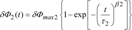
In light of this new term δΦ2(t), the true leakage current is thus given by equation [7.24]:
[7.24] ![]()
Figure 7.35. Band diagram of the metal/PZT/metal before (a) and after (b) resistance restoration

We have discussed in section 7.6.1 that the first barrier-lowering δΦ1, derived from the creation of space charge zones at the interfaces, is caused by the migration of oxygen vacancies ![]() (Figure 7.35a). The restoration phenomenon, which is opposed to the degradation, can be interpreted as the neutralization of these space charge areas. The positive charges Vo++ would be neutralized by the injection of electrons at the cathode, while the holes injection at the anode side would ensure the neutralization of negative charges. At the end of the restoration process, the barrier is heightened by a term δΦmax2 to reach a level Φfin= Φini − δΦmax 1 +δΦmax2 (Figure 7.35b).
(Figure 7.35a). The restoration phenomenon, which is opposed to the degradation, can be interpreted as the neutralization of these space charge areas. The positive charges Vo++ would be neutralized by the injection of electrons at the cathode, while the holes injection at the anode side would ensure the neutralization of negative charges. At the end of the restoration process, the barrier is heightened by a term δΦmax2 to reach a level Φfin= Φini − δΦmax 1 +δΦmax2 (Figure 7.35b).
An example of the I(t) characteristic simulation involving the resistance restoration phenomenon is shown in Figure 7.36. At 220°C, under a voltage of 5 V, almost half a decade of current separates the level Jmax from the level Jfin obtained after the end of the restoration.
For a complete model of leakage current evolution, the values of the characteristic parameters of the restoration process have to be determined: r2, β2, and δΦmax2, as well as the evolution of these parameters as a function of the temperature and the voltage level.
Figure 7.36. Modeling of the I(t) characteristic obtained at 5 V, 220°C, polarity +/TE. The final model (−) takes into account the resistance restoration observed after degradation (-·-) to fit the measurement (O)

7.6.2.2. Temperature activation of resistance restoration
Figures 7.39 and 7.41 provide the I(t) characteristics network obtained for a voltage of 5 V, in both polarity configurations, for temperatures ranging from 25°C to 240°C. The extraction of the characteristic parameters of the resistance restoration is performed on the curves obtained above 180°C, for which the restoration process is nearly completed. These parameters are then reinjected at low temperatures to achieve the simulation results shown in a continuous line. The parameters δΦmax2 and β2 defined in equation [7.23], respectively, denote the magnitude of the restoration and its slope. Only the parameter r2, denoting the kinetics of restoration, is thermally activated as shown in Figures 7.40 and 7.42.
The extracted values of the main parameters of resistance restoration are given in Table 7.3. The activation energy associated with the parameter τ2 is estimated at 1.34 ± 0.05 eV in both polarity configurations. This value of activation energy is consistent with a mechanism of holes trapping by deep centers such as the lead vacancies ![]() or other impurities of transition metal type [ALS 96]. This result is thus consistent with the hypothesis of a resistance restoration based on the neutralization of negative charges by the injection of holes at the PZT/anode interface.
or other impurities of transition metal type [ALS 96]. This result is thus consistent with the hypothesis of a resistance restoration based on the neutralization of negative charges by the injection of holes at the PZT/anode interface.
Figure 7.37. I(t) curves’ network obtained at 5 V (polarity +/TE) from 25°C to 240°C, by step of 15°C or 20°C. Experimental and modeled results taking into account the relaxation currents, the degradation of the true leakage current, and the resistance restoration phenomena

Figure 7.38. Evolution of τ2 parameter as a function of the temperature at 5 V in polarity -/TE: Arrhenius representation. Ea = 1.36 ±0.05 eV

Figure 7.39. I(t) curves’ network obtained at 5 V (polarity -/TE) from 25°C to 240°C, by step of 15°C or 20°C. Experimental and modeled results by taking into account the relaxation currents, the degradation of the true leakage current, and the resistance restoration phenomena

Figure 7.40. Evolution of τ2 parameter as a function of the temperature at 5 V in polarity -/TE: Arrhenius representation. Ea = 1.32 ± 0.05 eV
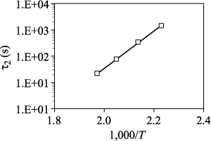
Table 7.3. Characteristic parameters of the resistance restoration determined by the modeling of I(t) characteristics obtained at 5 V from 180°C to 240°C
| Positive polarity on the top electrode | Negative polarity on the top electrode |
| δΦmax 2 = 0.06 ± 0.01 eV β2= 0.51 ±0.05 τ2(T) = A·exp(Ea2/kT) With Ea2 = 1.36 ± 0.05 eV |
δΦmax2 =0.11 ±0.01 eV β 2= 0.60 ±0.05 τ2(T)=A·exp(Ea2/kT) With Ea2= 1.32 ± 0.05 eV |
7.6.2.3. Influence of voltage on the resistance restoration
The final step of our modeling work concerns the evolution of the parameters specific to the resistance restoration as a function of the applied voltage level.
Figure 7.41. I(t) curves’ network obtained at 125°C, in negative polarity applied on top electrode from 3 to 16 V. Experimental and modeled results taking into account the relaxation currents, the resistance degradation, and the resistance restoration phenomena

Figure 7.42. Evolution of the τ2 parameter as a function of the applied voltage in negative polarity applied on top electrode, at 125°C. Logarithmic representation

Figure 7.41 shows an I(t) characteristics network measured at 125°C, for voltages ranging from 3 V to 16 V, in negative polarity applied to the top electrode. The restoration parameters δΦ2, β2, and τ2 are extracted from the curves at 12, 14, and 16 V to be reinjected into the modeling of the characteristics obtained at lower voltages. The parameters δΦmax 2 and β2 are independent of the voltage level while r2 can be modeled by a power law of the form: ![]() , with k2 = 3.8 ±0.3 (Figure 7.44).
, with k2 = 3.8 ±0.3 (Figure 7.44).
7.6.3. Conclusion
By analyzing the I(t) characteristics obtained at different voltage and temperature levels, we developed a behavioral model describing the dynamic evolution of the leakage current. The characteristics obtained at low voltages and/or low temperatures have first enabled to extract the parameters of the relaxation current (section 7.4). The characteristic parameters of the resistance degradation were then determined from the acquisitions performed at intermediate voltage and temperature levels (section 7.6.1). Finally, the resistance restoration phenomenon has also been modeled from the measurements taken at highest voltage and temperature levels (section 7.6.2).
In the next section, we propose to check the consistency of our dynamic model by analyzing the so-called “static” I(V) characteristics. The interpretation of these measurements is based on a space-charge influenced-injection model. This model allows us to supplement the current modeling at low voltages by taking into account the effect of space charge on the carriers’ injection.
7.7. Static characterization of the true leakage current: I(V,T)
7.7.1. Space-charge influenced-injection model
The space-charge influenced-injection model developed by Stolichnov and Tagantsev [STO 98a, STO 98b, STO 98c] is based on a hybrid conduction mechanism in which the charge transport is controlled by both the interfaces and the bulk of film. We have discussed in section 7.6 that the current density was significantly dependent on the sign of the applied polarity. It is, therefore, reasonable to consider a conduction mode limited by the interfaces. On the other hand, many studies mention the existence of a conduction regime limited by space charge for PZT [HUH 94, MAS 04, SCO 94, SUD 94]. Stolichnov and Tagantsev have therefore suggested considering the effect of this space charge on the injection and transport of carriers.
Concerning the nature of the injected carriers, it may be recalled that the barrier height calculations realized by Wouters et al. [WOU 95b] enhance the holes injection at the expense of electrons, while Scott et al. mention, on the contrary, a conduction governed by electrons [SCO 94]. This confusion results from the lack of precise information about the location of the Fermi level of PZT and the possible pinning of Fermi level by interface states. Stolichnov and Tagantsev experimentally removed this uncertainty by comparing the I(V) characteristics of structures featuring top electrodes of different nature, but keeping identical bottom electrodes. The level of the current density is then altered by the modification of the top electrode material when it is positively polarized, while it is invariant in negative polarity. This experiment demonstrates that the injection is governed by the anode, and thus it highlights an injection of holes.
Considering the fact that the work function of platinum is higher than that of PZT [WOU 95a], the contact between these two materials creates a positive space charge in PZT film. This space charge, assumed to be homogeneous in the film thickness, can be attributed to the presence of positively charged oxygen vacancies as well as other deep trap centers. The existence of this positive space charge results in an upward band curvature at the interfaces, as shown in Figure 7.43a.
When no potential difference is imposed across the structure (a), the energy barrier height is the sum of two contributions: Φh, which denotes the energy difference between the top of the valence band of PZT and the Fermi level of the anode, and ΔΦ, resulting from the band curvature caused by the space charge.
When voltage increases, the peak of the band curvature moves toward the anode, thus leading to a decrease in ΔΦ (b). Such an injection regime is called “ohmic” regime.
Figure 7.43. Band diagram of a metal/PZT/metal structure, with no applied field (a), in ohmic regime (b), in “static” Schottky regime (c), and in “dynamic” Schottky regime after resistance degradation/restoration (d)

Beyond a critical field ECr, the maximum potential barrier reaches the interface and the conduction is then governed by a traditional Schottky mechanism (c), with a barrier lowering ΔΦ induced by the image force and the applied voltage. The critical field ECr marks the transition between the ohmic and Schottky regimes.
In the Schottky configuration, Figure 7.43d helps us to recall the impact of the migration of oxygen vacancies on the band curvature at the interfaces when a prolonged stress is applied, as detailed in section 7.6.1.
7.7.2. Quantitative description of the model
The general expression giving the evolution of the energy profile Φ(x) of the valence band as a function of the applied field is given by equation [7.25]:
[7.25] ![]()
where x denotes the distance from the anode, Eext the applied electric field, e the electron charge, εS and εi the dielectric constants of PZT at low frequency and optical frequencies, respectively, ε0 the dielectric permittivity of the vacuum, and ρ the space charge density in the film. Assuming that the space charge is homogeneous in the thickness d of the film, the internal field Ebi created by the space charge at the interfaces is written as Ebi = dρ/2εSε0.
The first two terms on the right-hand side of equation [7.25] describe the band curvature caused by the space charge and its evolution with the applied field. These terms satisfy Poisson relationship for electrostatics:
[7.26] ![]()
The third term of equation [7.25] corresponds to the barrier lowering by the image force (Schottky effect), already discussed in section 7.2.2.1.
In general, the barrier height to be overcome by the carriers consists of two contributions: Φ0 = Φh + ΔΦ, with Φh the energy difference between the Fermi level of the anode and the valence band of PZT, and ΔΦ, which reflects the effect of the space charge or the effect of the image force depending on the ohmic or Schottky regime type.
7.7.2.1. Ohmic regime
In the ohmic regime (Figure 7.43b), the peak of the band curvature can be considered as far as sufficiently away from the interface to neglect the Schottky effect. In this case, by introducing the term Ebi = dρ/2εsε0 in equation [7.25], the energy profile can be rewritten as follows:
[7.27] 
The potential barrier for the carriers’ injection is maximal at the peak of the band curvature. The maximum curvature xm must satisfy the relation dΦ(x)/dx = 0. After derivation, we obtain the following expression for xm:
[7.28] ![]()
The barrier height ΔΦ caused by the space charge can thus be determined by injecting the value of xm given by equation [7.28] into the expression of the energy profile of equation [7.27]. This gives the following expression for ΔΦ:
[7.29] 
7.7.2.2. Static Schottky regime
When the applied electric field becomes greater than the internal electric field generated by the space charge (Eext > Ebi), the band diagram of the structure reaches the shape shown schematically in Figure 7.43c. In this configuration, the term resulting from the space charge can be neglected in equation [7.25] while the image force completely stays neutral. The injection of carriers then follows the traditional Schottky model with a correction in the expression of the barrier height lowering, due to the presence of the internal field Ebi at the interface:
[7.30] 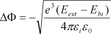
Considering the classical expression of the current resulting from a thermoionic emission of carriers over a potential barrier, the final model can be described by equation [7.31], where ΔΦ is given by relations [7.29] and [7.30] depending on the ohmic or Schottky regime type:
[7.31] ![]()
7.7.2.3. Dynamic Schottky regime
The space-charge influenced-injection model defined by Stolichnov and Tagantsev is purely static in that it does not take into account the evolutions of the band curvature induced by the resistance degradation and restoration phenomena. We thus propose to supplement this model by implementing the terms δΦ1(t) and δΦ2(t) defined in section 7.6:
[7.32] ![]()
Equations [7.33]–[7.35] describe the level of the currents Jini, Jmax, and Jfin obtained, respectively, before the start of the degradation (δΦ1 = δΦ2 = 0), at the peak of the degradation (δΦ1 = δΦmax1; δΦ2 = 0), and after the resistance restoration (δΦ1 = δΦmax1; δΦ2 = δΦmax2):
[7.33] ![]()
[7.34] ![]()
[7.35] ![]()
7.7.3. Static modeling Jmin(V) and Jmax(V)
7.7.3.1. Experimental procedure
Figure 7.44. Modeling of I(t) characteristics obtained under 5Vat140°C in polarity +/TE (−). The relaxation component (− −) is added to the true leakage current (-.·-) to fit the measurement(O)

We seek to verify the correct behavior of the space-charge influenced-injection model, by adjusting the I(V) measurements representative of the minimum and maximum level of the currents Jmin and Jmax. These levels of current correspond to regions of quasi-stability in which a static characterization approach is possible.
To characterize in static mode the evolution of the leakage current, we apply the staircase procedure for acquisition of the I(V) curves, as defined in section 7.3.1.1. In this acquisition mode, the determination of the appropriate step duration is essential to adequately characterize the true leakage current. Initially, we choose to acquire measurements at a temperature of 140°C.
Figure 7.44 presents the modeling results of I(t) curves obtained at 140°C under 5 V, in positive polarity applied to the top electrode. From this time evolution, the use of time switching levels of 10 s is sufficient to eliminate relaxation currents and to obtain the values of Jmin(V).
To characterize the maximal stage of current Jmax(V), we use as a first step a prestress of 5 V at 140°C for 600 s across the sample. After these 600 s, the level Jmax is reached: the oxygen vacancies have migrated to the interface and the degradation process is completed. Given the reversibility nature of the degradation, it is essential to proceed with the acquisition Jmax(V) immediately after the end of the pre-stress. The time-switching level used for this acquisition Jmax(V) is kept at 10 s, which is more than enough to neglect the contribution of the relaxation current relative to the level of Jmax.
7.7.3.2. Modeling results
The characteristics Jmin(V) and Jmax(V) are shown in Figure 7.45. They are obtained experimentally at a temperature of 140°C, according to the staircase procedure from 0 V to 12 V by a step of 0.2 V and time-switching level of 10 s, in positive polarity applied to the top electrode.
The results of the measurement’s adjustment by the space-charge influenced-injection model are also shown in this graph.
Concerning the Jmax(V) curve, we can point out the good behavior of the model over the entire voltage range studied. For the characteristic Jmin(V), however, the adjustment is satisfactory although only up to 3–4 V. Then, the flow of current weakens and ends up reaching the level of Jmax(V). This behavior, already discussed in section 7.3.2, can be attributed to the resistance degradation phenomenon that occurs during the acquisition process. The degradation process could be observed from 3 to 4 V and terminates around 8−10 V. The level of the current Jmin(V) reached at the end of the degradation process is very close to the level of Jmax(V) current for which the migration process of oxygen vacancies was forced during the pre-stress period.
Figure 7.45. Jmin(V) and Jmax(V) characteristics adjusted by the space-charge influenced-injection model. Staircase acquisition process from 0 to 12 V, by step of 0.2 V scan, with levels switching times of 10 s, at a temperature of 140°C
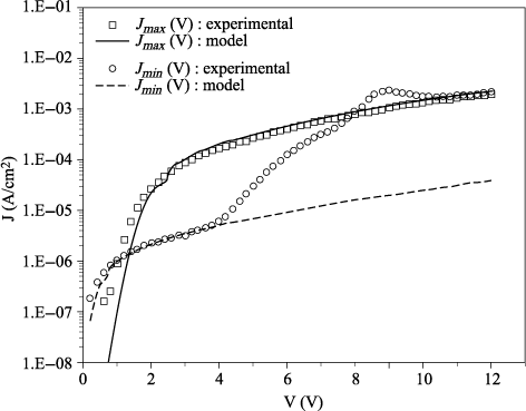
7.7.3.3. Discussion: consistency of the model
The parameters extracted from the adjustment of the static characteristics I(V) are summarized in Table 7.4. For comparison, Table 7.4 also includes the results obtained from the modeling of the dynamic characteristics I(t). To compare the results obtained from both the approaches, it is essential to standardize the parameters used to describe the static [7.32] and dynamic [7.24] models. The term Φini, introduced in the dynamic modeling, represents the effective barrier height before degradation. This term, therefore, includes the quantities Φh and ΔΦ introduced in the static model: Φini = Φh + ΔΦ. For a voltage of 5 V, the Schottky lowering ΔΦ is estimated at 0.08 eV.
Table 7.4. Energy barrier heights at IrO2/PZT contact from the static and dynamic modeling approaches
| Static modeling J(V) [V=0−12V,T=140°C] |
Dynamic modeling I(t) [V=5V,T = 25−240°C] |
| Barrier height after degradation: Φh−δΦmax 1 = 0.95± 0.05 eV derived from Jmax (V) | Barrier height after degradation: Φh−δΦmax 1 = 0.90± 0.05 eV derived from Jmax (T) |
| Barrier height during the degradation: Φh−δΦ = 1.11 ± 0.05 eV derived from Jmin(V) | Barrier height before the degradation: Φh= 1.23 ± 0.05 eV derived from Jini (T) |
| Lowering of barriers between Jmin and Jmax: δΦ = 0.15 eV derived from the ratio Jmax (V)/Jmin ( V) | Maximum lowering barrier: δΦmax1=033eV derived from the ratio Jmax(V)/Jini(V) |
The main comparison point to be observed, to verify the consistency of the results obtained from the static and dynamic approaches, is the barrier height after degradation (Φh−δΦmax1) estimated at 0.95 eV and 0.90 eV. This gap of 0.05 eV is relatively small, but the less reliable estimation is probably that given by the static modeling. In fact, the pre-stress applied before the acquisition ofJmax (V) is known to ensure that the maximum lowering δΦmax is reached, but the resistance restoration phenomenon that occurs during the acquisition should also be taken into account. Considering the maximum amplitude of restoration δΦmax2 evaluated in section 7.6.1.3 to 0.06 eV, it is totally acceptable to obtain through static modeling a barrier height between 0.90 and 0.96 eV.
The second parameter to look at in Table 7.4 is the barrier height Φh that governs the injection of the true leakage current Jini before degradation. This barrier height is estimated from the dynamic modeling at 1.23 eV. In the static approach, the initial level of true leakage current Jini is obscured by the relaxation current. It is thus the minimum current Jmin (V) that is characterized. However, as shown in Figure 7.44, the degradation process is already well underway when the level Jmin is reached. Accordingly, the parameter Φh cannot directly be extracted from the static model, and hence only the barrier height associated with the evolution Jmin (V) can be evaluated (Φh−δΦ). The adjustment of the Jmin (V) characteristic reveals a barrier height of 1.11 eV. This result means that the lowering process has already reached 0.12 eV when the current Jmin is reached (δΦ= 1.23 − 1.11 = 0.12 eV). This lowering represents 38% of the maximum lowering obtained at the end of the degradation (δΦmax1 = 0.32 eV).
7.7.3.4. Temperature modeling of Jmax(V)
As the phenomenon of degradation occurs during the acquisition of Jmn(V) curves, it makes sense to focus on the static modeling study based on the Jmax (V) characteristics. Figures 7.46 and 7.47 show the evolution of the Jmax (V) characteristics adjusted by the space-charge influenced-injection model for temperatures ranging from 45°C to 155°C.
Pre-stresses under a constant voltage of 5 V for 200 s at 155°C have previously been applied to reach and characterize the level of current Jmax. As for the I (V) acquisitions, performed at temperatures below 155°C, the cooling of samples that follows the pre-stress was carried out under a constant voltage of 1 V to avoid the problem of degradation reversibility. The experimental measurements were recorded by applying the staircase type acquisition procedures from 0 to 12 V, by steps of 0.2 V. Switching times of 1 and 10 s are imposed, respectively, for temperatures of 155°C and 125°C, while 100 s are applied for temperatures of 85°C and 45°C. The adaptation of step duration, depending on the temperature level, is essential so that the contribution of relaxation current might be eliminated, while avoiding the initiationof resistance restoration process.
It can be seen from Figures 7.46 and 7.47 that the modeling of the I(V,T) curves is pretty satisfying for temperatures of 85°C, 125°C, and 155°C, whereas the characteristics obtained at 45°C are not adjusted well comparatively. This difference between the simulated and experimental data can be explained by an inappropriate choice of the applied duration steps. In fact, we can check from the I(t) characteristics’ networks in Figures 7.37 and 7.39 that at 85°C, 100 s of stresses at 5 V are indeed enough to achieve a difference of more than one decade between the level Jmax and the relaxation current value. At 45°C, however, the relaxation current is of the order of same magnitude as the level Jmax after 100 s of stress. It thus makes sense to find a difference of a factor 2 based on the results of static modeling. The use of step durations of 1,000 s would have been more appropriate to completely get rid of the relaxation component at 45°C.
While the amplitude of the degradation represented by the parameter δΦmax 1 is highly dependent on the applied polarity sign, the energy barrier heights obtained after degradation are found to be almost symmetrical. The adjustment of the Jmax (V, T) curves leads to a value of 0.95 ± 0.02 eV for Φh after degradation in both the polarity configurations. The static dielectric constant ei that controls the voltage dependence is estimated to be 2.7. This constant corresponds to the square root of the optical index. The value of 2.7 for ei is relatively small compared to most theoretical values reported in the literature (from 4.5 to 7) [BOE 00, KAL 91, STO 00], but it is consistent with the results published by Boerasu et al. [BOE 03].
Figure 7.46. Jmax(V) characteristics at 45°C, 85°C, 125°C, and 155°C adjusted by the spacecharge influenced-injection model. A positive polarity is applied on the top electrode

Figure 7.47. Characteristics Jmax(V) at 45°C, 85°C, 125°C, and 155°C adjusted by the spacecharge influenced-injection model. A negative polarity is applied on the top electrode

7.8. Conclusion
This chapter presents a detailed study of the leakage current conduction mechanisms in PZT capacitor structures, obtained by sol-gel deposition. In the first section, we endeavored to present the major conduction modes specific to metal/insulator/metal structures, by recalling the evolution laws I(V,T) characteristics of these conduction modes.
The method generally used to characterize the leakage current conduction in a new structure is to compare the experimental I(V, T) curves with the different theoretical models to identify the best-suited model. Unfortunately, in the case of PZT capacitors, as in the case of any material that presents an evolution of doping or interface states over time, the instability of the leakage current makes the study more complex. In the second section, we illustrated the difficulty of establishing experimental procedures allowing the acquisition of stable I(V) characteristics. Besides the existence of relaxation currents that disturb the measurement of true leakage current, we highlighted the successive phenomena of resistance degradation and resistance restoration that modify the injection parameters of the leakage current over time. Therefore, given the difficulty of acquiring and interpreting the I(V) characteristics, we opted for a strategy of characterization based on the analysis of I(t) curves obtained at different voltage and temperature levels.
The modeling of the relaxation current was first performed in the third section, from the I(t) characteristics measured at low voltage and temperature stresses. Then, a complete characterization of the resistance degradation and restoration was carried out in the fifth section, based on the time evolution of current density at highest voltage and temperature levels. The “dynamic” model thus obtained makes it possible to describe the leakage current evolution as a function of time, temperature, and applied voltage. This model is based on a Schottky injection of carriers at the PZT/anode, governed by an energy barrier that presents some height variation over time. The first evolution term δΦ1(t) is attributed to a phenomenon of migration of oxygen vacancies that alters the space charge distribution at the interfaces and results in a lowering of the barrier height: the resistance degradation. It is important to note here that there is very little direct experimental evidence concerning the migration of oxygen vacancies. However, the reasoning remains valid considering a migration of the electronic space charge associated with these vacancies. The consistency of this scenario of degradation has been validated through several characterization results: capacitive measurements, activation energies, and influence of the nature of the electrodes. In a second step, a partial restoration of the resistive properties of the structure was observed. This restoration was considered in the model by introducing a second evolution term δΦ2(t) which is opposed to the first lowering of the barrier. The physical origin of this phenomenon of restoration was attributed to the neutralization of a certain amount of fixed charges at the interfaces by carriers’ injection.
Table 7.5. Complete model of leakage current evolution as a function of time under stress t, of the temperature T and the applied voltage V

In the last section, the static space-charge influenced-injection model was introduced. This model, fully consistent with the dynamic model developed in the previous section, allows us to describe the leakage current evolution over a wide voltage range, by including the so-called “ohmic” regime at low voltages. The highly acceptable difference between the results extracted from the adjustment of static and dynamic measurements proves the consistency of the global model.
Table 7.6. Parameters of leakage current model described in Table 7.5. The parameters Ebiav and Ebiap represent the internal electric fields generated by the space charge, respectively, before and after the resistance degradation

Our final model is described by the equations shown in Table 7.5, while the adjustment parameters extracted from the different modeling steps are summarized in Table 7.6. The development of such a behavioral model presents an obvious industrial interest. It is indeed very important to develop a predictive model capable of determining the maximal leakage current level likely to be reached by a capacitor depending on its application conditions.
7.9. Bibliography
[ALS 96] AL-SHAREEF H., DIMOS D., Proceedings of the 10th IEEE International Symposium on the Application of Ferrolectrics ISAF, 1996.
[BAI 90] BAIATU T., WASER R., HÄRDTL K.H., “Electrical degradation of perovskite-type titanate: III, A model of the mechanism”, Journal of American Ceramic Society, vol. 73, no. 6, pp. 1663–1673, 1990.
[BAN 03] BANIECKI J. D., SHIOGA T., KURIHARA K., KAMEHARA N., “Investigation of the importance of interface and bulk limited transport mechanisms on the leakage current of high dielectric constant thin film capacitors”, Journal of Applied Physics, vol. 94, p. 6741, 2003.
[BAR 86] BARBOTTIN G., VAPAILLE A., Instabilities in Silicon Devices, Silicon Passivation and Related Instabilities, North Holland, Amsterdam, vol. 1, 1986.
[BOE 00] BOERASU I., PEREIRA M., GOMES M.J.M., FERREIRA M.I.C., “Structural and optical characterization of Nb-doped Pzt 65/35 thin films grown by sol-gel and laser ablation techniques”, Journal of Optoelectronics and Advanced Materials, vol. 2, p. 602, 2000.
[BOE 03] BOERASU I., PINTILIE L., PEREIRA M., VASILEVSKIY M. I., GOMES M.J.M., “Competition between ferroelectric and semiconductor properties in Pb(Zr0.65Ti0.35)O3 thin films deposited by sol-gel”, Journal of Applied Physics, vol. 93, no. 8, 2003.
[BUN 51] BUNTING E.N., SHELTON G.R., CREAMER A. S., JAFFE B., “Properties of berylliumbarium titanate dielectrics”, Journal of Research of the National Bureau Of Standards, vol. 47, pp. 15–24, 1951.
[CHA 76] CHAN N.H., SMYTH D.M., “Defect chemistry of BaTiO3”, Journal of Electrochemical Society, vol. 123, no. 10, pp. 1584–1585, 1976.
[CHE 93] CHEN X., KINGON A.I., MANTESE L., AUCIELLO O., HSIEH K.Y., “Characterization of conduction of PZT thin films produced by laser ablation deposition”, Integrated Ferroelectrics, vol. 3, pp. 355–363, 1993.
[CHE 94a] CHEN X., KINGON A.I., AL-SHREEF H., BELLUR K.R., “Electrical transport and dielectric breakdown in Pb(Zr,Ti)O3 thin films”, Ferroelectrics, vol. 151, pp. 133–138, 1994.
[CHE 94b] CHEN X., KINGON A. I., BELLUR K., AUCIELLO O., “DC leakage and failure of PZT thin film capacitors for non-volatile ferroelectric memory and DRAM applications”, Integrated Ferroelectrics, vol. 5, pp. 59–72, 1994.
[CHE 98] CHEN H.M., TSAUR S.W., LEE J.Y.M., “Leakage current characteristics of lead-zirconate-titanate thin film capacitors for memory device applications”, Journal of Applied Physics, vol. 37, pp. 4056–4060, 1998.
[CHE 08] CHENTIR M.T. et al., “Electrical characterization and reliability of lanthanum doped PZT thin films capacitors”, Integrated Ferroelectrics, vol. 96, no. 1, pp. 75–81(7), 2008.
[DES 93] DESU S.B., YOO I.K., “Electrochemical models of failure in oxide perovskytes”, Integrated Ferroelectrics, vol. 3, pp. 365–376, 1993.
[DES 95] DESU S.B., “Minimization of fatigue in ferroelectric films”, Physica Status Solidi, (a), vol. 151, p. 467, 1995.
[DES 99] DESU C.S., VEDULA R., LEE K.B., DESU S.B., “Electrical properties of PZT thin film capacitors with novel Pt-Ir based electrode barriers for nonvolatile memories”, Materials Research Society, vol. 541, pp. 71–75, 1999.
[DEY 96] DEY K., DANS PAS DE ARAUJO C., SCOTT J.F., TAYLOR G.W (ed.), Ferroelectric Thin Films: Synthesis and Basic Properties, Gordon and Breach, Amsterdam, pp. 329–386, 1996.
[DIE 95] DIETZ G.W., WASER R., “How to analyse relaxation and leakage currents of dielectric thin films: Simulation of voltage-step and voltage-ramp techniques”, Integrated Ferroelectrics, vol. 9, pp. 317–332, 1995.
[DSH 03] D-SHYE C., CHIOU B.S.B., LAI M.J., HWANG C.C., JIANG C.C., CHEN J.S., CHENG M.H., CHENG H.C., “Low Temperature Radio-Frequency-Sputtered (Ba, Sr)TiO3 Films on Pt/TiN/Ti/Si Substrates with Various Oxygen/Argon Mixing Ratios”, Journal of the Electrochemical Society, vol. 150, no. 2, pp. F20–F27, 2003.
[HOF 97] HOFMAN W., HOFFMAN S., WASER R., “Dopant influence on dielectric losses, leakage behaviour, and resistance degradation of SrTiO3 thin films”, Thin Solid Films, vol. 305, pp. 66–73, 1997.
[HUH 94] HU H., KRUPANIDHI S.B., “Current-voltage characteristics of ultrafine-grained ferroelectric Pb(Zr, Ti)O3 thin films”, Journal of Materials Research, vol. 9, no. 6, pp. 1484–1498, 1994.
[JON 83] JONSCHER A.K., Dielectric Relaxation in Solids, Chelsea Dielectrics Press, London, 1983.
[KAL 91] KALA T., “Electronic properties of Pb(ZrTi)O3 solid solutions”, Phase Transitions, vol. 36, pp. 65–88, 1991.
[KIM 02] KIM S.H., WOO H.J., KOO C.Y., YANG J.S., HA S.M., PARK D.Y., “Effect of heterostructure electrodes on the reliability of ferroelectric PZT thin films”, Journal of the Korean Ceramic Society, vol. 39, no. 4, pp. 341–345, 2002.
[KOT 99] KOTECKI D.E. et al., “(Ba,Sr)TiO3 dielectrics for future stacked-capacitors DRAM”, IBM Journal of Research and Development, vol. 43, no. 3, 1999.
[KUR 01] KURASAWA M., KURIHARA K., OTANI S., KUTAMI M., “Retention and imprint properties in single crystalline PLZT thin film capacitors”, Proceedings of the 12th IEEE International Symposium on the Application of Ferroelectrics ISAF, Honolulu, Hawaii, 2001.
[LEE 01] LEE K., RHEE B.R., LEE C., “Characteristics of ferroelectric Pb(Zr,Ti)O3 thin films having Pt/PtOx electrode barriers”, Journal of the Korean Physical Society, vol. 38, no. 6, pp. 723–728, 2001.
[MAS 04] MASUDA Y., NOZAKA T., “Investigation into electrical conduction mechanisms of Pb(Zr,Ti)O3 thin-film capacitors with Pt, IrO2 and SrRuO3 top electrodes”, Japanese Journal of Applied Physics, vol. 43, no. 9B, pp. 6576–6580, 2004.
[MIH 95] MIHARA T., WATANABE H., “Electronic conduction characteristics of sol-gel ferroelectric Pb(Zr0.4Ti0.6)O3 thin-film capacitors”, Japanese Journal of Applied Physics, vol. 34, pp. 5674–5682, 1995.
[MOA 90] MOAZZAMI R., HU C., SHEPHERD W., “Electrical conduction and breakdown in solgel derived PZT thin films”, IEEE Proceedings of the 28th Annual Proceedings Reliability Physics Symposium, p. 231, New York, 1990.
[NEU 86] NEUMANN H., ARLT G., “Transient Polarization Currents and Degradation Effects in BaTiO3 and SrTiO3 Ceramics”, Proceedings of the 6th Symposium. Applications of Ferroelectricity, Bethlehem, p. 357, PA IEEE, Piscataway, NJ, 1986.
[NUM 95] NUMATA K., FUKUDA Y., AOKI K., NISHIMURA A., “Analysis of the resistance degradation of SrTiO3 and BaxSr(1−x)TiO3 thin films”, Japanese Journal of Applied Physics, vol. 34, pp. 5245–5249, 1995.
[RYO 03] RYOO S.N., YOON S.G., KIM S.H., “Improvement in ferroelectric properties of Pb(Zr0.35Ti0.65)O3 thin films using a Pb2Ru2O7-x conductive interfacial layer for ferroelectric random access memory application”, Applied Physics Letters, vol. 83, no. 14, 2003.
[SAH 00] SAHA S., KRUPANIDHI S.B., “Impact of microstructure on the electrical stress induced effects of pulsed laser ablated (Ba,Sr)TiO3 thin films”, Journal of Applied Physics, vol. 87, no. 6, 2000.
[SCH 76] SCHAFFRIN C., “Oxygen diffusion in BaTiO3 ceramic”, Physica Status Solidi, (a), vol. 35, p. 79, 1976.
[SCO 93] SCOTT J.F., MELNICK B.M., MCMILLAN L.D., PAZ DE ARAUJO C.A., “Dielectric Breakdown in High-ε Films for ULSI DRAMs”, Integrated Ferroelectrics, vol. 3, pp. 225–243, 1993.
[SCO 94] SCOTT J.F., AZUMA M., PAZ DE ARAUJO C.A., MCMILLAN L.D., SCOTT M.C., ROBERTS T., “Dielectric Breakdown in High-ε Films for ULSI DRAMs II: Barium Strontium Titanate Ceramics”, Integrated Ferroelectrics, vol. 4, pp. 61–84, 1994.
[SEU 74] SEUTER A.M., Defect chemistry and electrical transport properties of barium titanate, Philips Research Report, Supplement, vol. 3, pp. 1–84, 1974.
[STO 98a] STOLICHNOV I., TAGANTSEV A., “Space-charge influenced-injection model for conduction in Pb(ZrxTi1−x)O3 thin films”, Journal of Applied Physics, vol. 84, p. 3216, 1998.
[STO 98b] STOLICHNOV I., TAGANTSEV A., COLLA E.L., SETTER N, “Cold-field-emission test of the fatigued state of Pb(ZrxTi1−x)O3 films”, Applied Physics Letters, vol. 73, p. 1361, 1998.
[STO 98c] STOLICHNOV I., TAGANTSEV A., SETTER N., Ferroelectrics, vol. 225, p. 147, 1998.
[STO 99] STOLICHNOV I., TAGANTSEV A., SETTER N., CROSS J.S., TSUKADA M., “Control of leakage conduction of high-fatigue-endurance (Pb, La)(Zr, Ti)O3 film ferroelectric capacitors with Pt/SrRuO3 electrodes”, Applied Physics Letters, vol. 75, 1999.
[STO 00] STOLICHNOV I., Interface-controlled mechanisms of degradation in ferroelectric thin films, Thesis, EPFL, 2000.
[SUD 94] SUDHAMA C., CAMPBELL A.C., MANIAR P.D., JONES R.E., MOAZZAMI R., MOGAB C.J., LEE J.C., “A model for electrical conduction in metal-ferroelectric-metal thin-film capacitors”, Journal of Applied Physics, vol. 75, pp. 1014–1022, 1994.
[WAL 67] WALTER L.C., GRACE R.E., “Formation of points defects in strontium titanate”, Journal of Physics and Chemistry of Solids, vol. 28, no. 2, pp. 239–245, 1967.
[WAS 90a] WASER R., BAIATU T., HÄRDTL K.H., “DC electrical degradation of perovskite-type titanate : I, ceramics”, Journal of the American Ceramic Society, vol. 73, no. 6, pp. 1645–1653, 1990.
[WAS 90b] WASER R., BAIATU T., HÄRDTL K.H., “Electrical degradation of perovskite-type titanate: II, single crystals”, Journal of the American Ceramic Society, vol. 73, no. 6, pp. 1654–1662, 1990.
[WAS 92] WASER R., KLEE M., “Theory of Conduction and Breakdown in Perovskite Thin Films”, Integrated Ferroelectrics, vol. 2, pp. 23–40, 1992.
[WAS 97] WASER R., “Dielectric analysis of integrated ceramic thin film capacitors dielectric analysis of integrated ceramic thin film capacitors”, Integrated Ferroelectrics, vol. 15, p. 39, 1997.
[WOU 95a] WOUTERS D.J., WILLEMS G.J., GROESENEKEN G., MAES H.E., BROOKS K., KLISSURSKA R., “The influence of dopants on the leakage current in PZT thin-film ferroelectric capacitors”, Science and Technology of Electroceramic Thin Films, pp. 279–289, 1995.
[WOU 95b] WOUTERS D.J., WILLEMS G.J., MAES H.E., “Electrical conductivity in ferroelectric thin films”, Microelectronic Engineering, vol. 29, pp. 249–256, 1995.
[YOO 92] YOO K., DESU S.B., “Leakage current mechanism and accelerated unified test of lead zirconate titanate thin film capacitors”, Proceedings of the 8th IEEE International Symposium on the Application of Ferroelectrics ISAF, 1992.
[ZAF 99] ZAFAR S., HRADSKY B., GENTILE D., CHU P., JONES R.E., GILLESPIE S., “Resistance degradation in barium strontium titanate thin films”, Journal of Applied Physics, vol. 87, no. 7, 1999.
[ZUR 99] ZURCHER P., TRACY C.J., JONES R.E., ALLURI P., CHU P.Y., JIANG B., “Barium Strontium Titanate Capacitors for Embedded Dram”, Material Research Society Symposium Proceedings, vol. 541, 1999.
1 Chapter written by Emilien BOUYSSOU.