
Chapter 12
Integration of Multiferroic BiFeO3 Thin Films
into Modern Microelectronics 1
12.1. Introduction
Multiferroic materials, which simultaneously display ferroelectric and magnetic ordering, have recently attracted a great deal of attention because of the intriguing science behind their magnetoelectric (ME) coupling phenomenon and their exciting application potential in multiple controlled devices [SPA 05, FIE 05, EER 06, RAM 07, GAJ 07]. By the original definition, such materials that possess two, or all three, of the so-called “ferroic” properties — ferroelectricity, ferromagnetism, and ferroelasticity — in the same phase are known as multiferroics [SPA 05, EER 06], and are depicted in Figure 12.1. However, the current trend is to exclude the requirement for ferroelasticity in practice and to broaden the classification of multiferroics by including antiferroic order such as antiferroelectricity and antiferromagnetism [EER 06]. Generally speaking, multiferroics can be classified into two groups on the basis of the microscopic mechanism that determines their properties [KHO 09]. The first group contains those materials in which ferroelectricity and magnetism have different sources and appear independently of each other, though there is some coupling between them. These materials are often good ferroelectrics with quite large spontaneous polarization (of order of magnitude 10–100 μC/cm2), and their critical temperatures of the magnetic and/or ferroelectric transitions can be well above the room temperature. Examples of the first group are BiFeO3 (BFO) (ferroelectric Curie temperature TC ~ 1,100 K, antiferromagnetic Néel temperature TN ~ 640 K, ferroelectric spontaneous polarization Ps ~ 100 μC/cm2), and YMnO3 (TC ~ 914 K, TN ~ 76 K, Ps ~ 6 μC/cm2). Unfortunately, the coupling between magnetism and ferroelectricity in these materials is usually rather weak. The challenge for the materials of this group of multiferroics is to retain all their positive features, while enhancing this coupling. The second group is the comparatively recently discovered multiferroic materials, in which magnetism, such as spiral spin order and magnetic exchange striction, induces ferroelectricity, implying a strong coupling between the two. However, the critical transition temperatures are usually very low and the ferroelectric polarization in these materials is also very small (~10−2 μC/cm2). Examples of the second group are TbMnO3 and TbMn2O5. It should be noted here that apart from single-phase multiferroic materials, there is another type of multiferroics, namely, composite multiferroics. Interestingly, it turns out that a strong ME coupling at room temperature can be obtained in composite multiferroics of thin-film architectures, which consist of known magnets and ferroelectrics in the form of multilayers (also called horizontal heterostructures), in which the principles of heteroepitaxy at the interfaces can be used to control and initiate ME coupling at the atomic scale, and self-organized nanostructures (also called nanoscale “vertical heterostructures”), in which coupling occurs through vertical heteroepitaxy [RAM 07, NAN 08].
The ME effect, in its most general definition, denominates the coupling between electric and magnetic fields in matter, i.e. induction of magnetization (M) by an electric field (E) or polarization (P) generated by a magnetic field (H) [FIE 05, WAN 09]. Thermodynamically, the ME effect can be understood within the framework of Landau theory and is thus described by the expansion of free energy for an ME system:
[12.1] 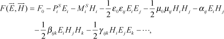
where F0 is the ground-state free energy, subscripts (i, j, k) the three components of a variable in spatial coordinates, Ei and Hi the components of the electric field ![]() and magnetic field
and magnetic field ![]() , respectively,
, respectively, ![]() and
and ![]() the components of spontaneous polarization PS and magnetization MS, ε0 and μ0 the dielectric and magnetic susceptibilities of vacuum, εij and μij the second-order tensors of dielectric and magnetic susceptibilities, βijk and γijk the third-order tensor coefficients and, most importantly, αij the component of tensor α, which is designated as the linear ME effect and corresponds to the induction of polarization by a magnetic field or a magnetization by an electric field. Differentiation leads to polarization:
the components of spontaneous polarization PS and magnetization MS, ε0 and μ0 the dielectric and magnetic susceptibilities of vacuum, εij and μij the second-order tensors of dielectric and magnetic susceptibilities, βijk and γijk the third-order tensor coefficients and, most importantly, αij the component of tensor α, which is designated as the linear ME effect and corresponds to the induction of polarization by a magnetic field or a magnetization by an electric field. Differentiation leads to polarization:
[12.2] ![]()
and to magnetization:
[12.3] ![]()
Unfortunately, the ME effect at room temperature in single-phase compounds, as mentioned above, is usually too small to be practically applicable. An approach to significantly enhance the ME response in single-phase compounds is to make use of strong internal electromagnetic fields in the components with large dielectric and magnetic susceptibilities. It is well known that ferroelectric/ferromagnetic materials possess the largest dielectric/magnetic susceptibility. As a result, ferroelectrics with ferromagnetism, namely, ferroelectromagnets, would be the prime candidates for seeking an enhanced ME effect. Up to date, among all single-phase multiferroic compounds, BiFeO3 has been the most extensively investigated compound and has had a great impact on the field of multiferroics as, perhaps, it is the only material that is both magnetic and a strong ferroelectric at room temperature (though the ME coupling is still weak) [CAT 09].
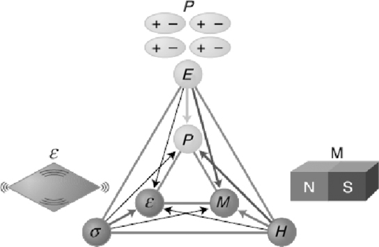
BiFeO3 is known to have very high ordering temperatures, that is, a ferroelectric Curie temperature (TC) of ~1,100 K and an antiferromagnetic Néel temperature (TN) of ~640 K [FIS 80, MIC 69]. Such a specific feature — that both TC and TN in BFO are far above the room temperature — is of great significance from a technological viewpoint. The room-temperature phase of BiFeO3 is classified as rhombohedral (space group R3c) [MOR 71]. The rhombohedrally distorted perovskite-type unit cell has a lattice parameter a of 3.965 Å and a rhombohedral angle α of 89.4° with ferroelectric polarization along [111] direction, as depicted in Figure 12.2 [KUB 90, EDE 05]. Recently, an intrinsic polarization of about 60 μC/cm2 was obtained in high-quality BFO single crystals, indicating that the [111]-oriented polarization can experimentally reach up to 100 μC/cm2 in BFO [LEB 07]. This is consistent with the theoretically predicted values (90–100 μC/cm2) [NEA 05]. On the other hand, BiFeO3 has a complicated magnetic configuration. It is generally accepted that bulk BFO is a G-type antiferromagnet, i.e. the Fe magnetic moments are coupled antiferromagnetically between adjacent planes. If the magnetic moments are oriented perpendicular to the [111] direction, the symmetry also permits a canting of the antiferromagnetic sublattices, resulting in a macroscopic magnetization, which is the so-called weak ferromagnetism [EDE 05]. However, the antiferromagnetic spin order is not spatially homogeneous but is rather a spatially modulated structure, manifested by an incommensurate cycloid structure of wavelength λ ~ 62 nm [SOS 82]. Owing to this feature, the antiferromagnetic vector is locked within the cycloid and averaged to zero over a scale of approximately λ, thereby leading to a cancellation of the macroscopic magnetization. This cycloidal spin modulation can also inhibit the observation of the linear ME effect; and instead, only a quadratic ME effect can be measured [POP 93]. It is believed that this cycloid structure may be partially destroyed if the sample size is reduced to the size of cycloid wavelength (~62 nm), leading to enhanced magnetization and ME coupling in nanoscale BFO samples, such as BFO nanowires and nanoparticles [MAZ 07, GAO 07].
Figure 12.1. Phase control in ferroics and multiferroics. Basically, the electric field E, magnetic field H, and stress σ control the electric polarization P, magnetization M, and strain ε, respectively. In a multiferroic, the coexistence of at least two ferroic forms of ordering leads to additional interactions. For instance, in a magnetoelectric multiferroic, a magnetic field may control P and vice versa, an electric field may control M (dark gray arrows). The coupling and mutual control between different ferroic forms of ordering represent the cores of multiferroicity [SPA 05]
In this chapter, we focus on thin films of BiFeO3 as the thin-film form has specific advantages in device integration. First, several preparation methods for obtaining phase-pure BiFeO3 thin films are presented and compared. Second, the fascinating multiferroic properties of BFO thin films, including ferroelectricity and magnetism, are discussed. Finally, great emphasis is placed on device applications, especially on spintronics and memory devices that can be addressed both electrically and magnetically.
Figure 12.2. Schematic view of the R3c structure for BiFeO3. The cations are displaced along the [111] direction relative to the anions, and the oxygen octahedra rotate with alternating sense around the [111] axis [EDE 05]
12.2. Preparation methods
Bismuth ferrite is very prone to show parasitic phases that tend to nucleate at grain boundaries and impurities [VAL 07]. A slight deviation from the ideal stoichiometry could lead to the formation of parasitic phases, such as Bi2O3, Fe2O3, Bi2Fe4O9, Bi24Fe2O39, Bi46Fe2O72, and Bi25FeO40 [BÉA 05, TER 06, LIU 06]. During synthesis, the kinetics of formation always leads to a mixture of BiFeO3 as a major phase along with other impurity phases of Bi and Fe. The problem becomes more complex when BiFeO3 is prepared in the thin film form. In consequence, preparation of phase-pure BiFeO3 thin films is indeed a challenging task. Nonetheless, the recent improvement in the techniques of thin film preparation makes it possible to obtain phase-pure BFO thin films. Particularly, the current interest in BFO was stimulated primarily by a science paper in 2003 from Ramesh's group [WAN 03], which showed that the epitaxial BFO thin films prepared by pulsed laser deposition (PLD) had unexpectedly large remnant polarization, Pr, 15 times larger than that previously observed in bulk, as well as very large ferromagnetism of ~1.0 Bohr magneton (μB) per unit cell. However, it was commented later that the strong ferromagnetism observed in BFO thin films by Ramesh and colleagues was not an intrinsic effect, but it was rather induced by a substantial Fe2+ fraction and oxygen vacancies, and the role of strain in the large enhancement of ferroelectric polarization and magnetization should be ruled out, and the intrinsic magnetization of BFO thin films should be much lower, near zero, ~0.02 μB/unit cell [EER 05, BÉA 06a]. Now, it is generally accepted that BFO is indeed a G-type antiferromagnet even in thin-film form, thus displaying intrinsically very weak magnetic responses. This is discussed in detail in the following context. Among various preparation methods, PLD and chemical solution deposition (CSD) are considered to be the two mainstream methods for preparing BFO thin films since they are powerful in precise control of thin film composition. In the following, we briefly review several methods that have been widely reported in literature for the preparation of BFO thin films, including PLD, CSD, and RF magnetron sputtering. It should be noted here that some other methods, such as metal organic chemical vapor deposition and molecular-beam epitaxy have also been tentatively used for the preparation of BFO thin films [UEN 05, KAR 07, IHL 07, IHL 08].
12.2.1. Pulsed laser deposition
Pulsed laser deposition is a thin film deposition (specifically a physical vapor deposition) technique in which a high-power pulsed laser beam is focused inside a vacuum chamber to strike a target of the material that is to be deposited. This material is evaporated in a plasma plume from the target (the plume is normal to the target surface) and deposited as a thin film onto a substrate. Figure 12.3 shows a schematic diagram of a basic PLD system. Lasers that are commonly used include ArF and KrF excimer lasers and Nd:YAG laser. The laser ablation process can occur in ultrahigh vacuum or in the presence of a background gas, such as oxygen which is commonly used when depositing oxides to fully oxygenate the deposited films. While the basic setup is simple relative to many other deposition techniques, the physical phenomena of laser–target interaction and film growth are quite complex. When the laser pulse is absorbed by the target, energy is first converted into electronic excitation and then into thermal, chemical, and mechanical energy, resulting in evaporation, ablation, and plasma formation, and even exfoliation [CHR 94]. Before depositing onto the typically hot substrate, the ejected species expand into the surrounding vacuum in the form of a plume containing many energetic species including atoms, molecules, electrons, ions, clusters, particulates, and molten globules.
Figure 12.3. Schematic illustration of a pulsed laser deposition system
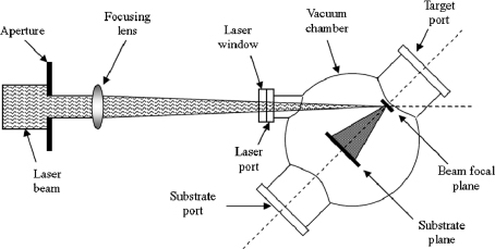
Figure 12.4. (a) (003) peaks from x-ray θ–2θ scans showing the effect of film thickness on heteroepitaxial strain. As the film thickness was increased from 70 to 400 nm, the peak position progressively increased (70 nm; 100 nm; 200 nm; 400 nm); (b) selected area electron diffraction pattern from a 200 nm thick BFO film, revealing a good crystalline quality with a structural distortion [WAN 03]
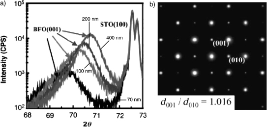
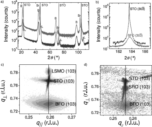
In 2003, it was demonstrated by Ramesh’s group that high-quality heteroepitaxial BFO thin films could be grown on SrRuO3-coated SrTiO3 substrates by PLD [WAN 03]. Large-angle x-ray scans confirmed the phase-pure quality, and a small section of the x-ray diffraction (XRD) spectra from films of varying thickness (Figure 12.4a) demonstrated the existence of heteroepitaxial strain in the BFO thin films. Selected area electron diffraction patterns (Figure 12.4b) as well as low-magnification bright field images confirmed the single crystalline quality of the BFO films. This pioneering work stimulated a significant research in the field of multiferroic thin films. After this, a large number of works were devoted to PLD of pure and doped BFO thin films, and abundant exciting results relating to the preparation and properties were obtained [BÉA 05, WAN 04, MAN 05, YUN 06, TAK 06, DHO 06, WAN 06, ZHA 06, LUO 07, BAR 07, RAN 07 CRU 07, LIM 07, KIM 08, CHE 08, ZHA 09, CHE 09]. It is particularly worth mentioning that Prof. Barthélémy’s group at the laboratory of UMP CNRS/Thales has made a significant contribution in this subject. High-quality epitaxial BFO films have been grown by PLD on La2/3Sr1/3MnO3 (LSMO)- or SrRuO3 (SRO)-coated single-crystal SrTiO3 (STO) and LaAlO3 substrates using a frequency tripled (λ = 355 nm) Nd:YAG laser at a frequency of 2.5 Hz; moreover, the effects of Mn doping, substrate type, film thickness, and film orientation have been well investigated [BÉA 05, BÉA 06a, BÉA 06b BÉA 06c, BÉA 06d, BÉA 07, BÉA 08a, BÉA 08b, BÉA 08c, ZHU 08, BÉA 08d, BÉA 09]. Generally, BFO and 5%-Mn-doped BFO (BFO–Mn) films were grown with an oxygen pressure of 6 × 10⁻³ mbar and at a substrate temperature of 580°C since these conditions allowed the growth of single-phase films. The BFO and BFO–Mn targets contained 15% excess Bi to compensate for its very high volatility. The crystalline structure of BFO thin films has been studied by high resolution XRD, using a PANalytical X’Pert PRO equipped with a Ge(220) monochromator. θ–2θ patterns, presented in Figure 12.5a, indicate a (00l) texture of both bilayers (BFO/LSMO and BFO/SRO) on the substrate. To study the in-plane orientation of the films, Ф scans we carried out around the (303) peaks of BFO and STO. Four peaks were obtained, separated by 90° and aligned with those of the substrate, indicating a cube-on-cube epitaxy of the bilayers. An example of such a peak is presented in Figure 12.5b for the BFO/SRO bilayer. The strain states of the bilayers have also been studied by performing reciprocal space mappings (RSM) around the (103) reflection, as shown in Figures 12.5c and 12.5d for the bilayers BFO/LSMO and BFO/SRO, respectively. All three peaks are aligned in the q// direction, indicating that the in-plane parameters of the BFO and the bottom electrode are same as the substrate lattice parameter. Both bilayers are, thus, fully strained on the STO substrate.
Figure 12.5. (a) θ–2θ x-ray diffraction pattern for 70 nm thick BFO films deposited onto LSMO(11 nm)||STO(001) (lower curve) and SRO(25 nm)||STO(001) (upper curve). The peaks are attributed to STO for the substrate, B for the BFO film, Sr for the SRO layer, and L for the LSMO film; (b) Ф scan around (3, 0, 3) peak for a BFO(70 nm)/SRO(25 nm)||STO(001) sample. (c) RSM around (103) reflection for BFO(70 nm) films deposited on LSMO (11 nm)||STO(001); (d) and SRO(25 nm)||STO(001) [BÉA 08d]
PLD has many advantages over other film deposition methods, which include the following:
1) It is versatile. A very wide range of materials, including oxides, metals, semiconductors, and even polymers, can be grown by PLD.
2) It has the ability to maintain target composition in the deposited thin films.
3) The energy associated with the high ionic content in laser ablation plume and high particle velocities can aid the crystal growth and lower the substrate temperature required for epitaxy.
4) PLD system is clean and capable of producing multilayers by simply switching between several different targets.
There are, however, some disadvantages of PLD, which include the following:
1) The ablation plume cross-section is generally small (of the order of cm2) owing to a limited laser spot size. This, in turn, limits the sample size that can be prepared by PLD. In addition, this also causes difficulty in controlling the thickness uniformity across the sample. Such a problem can be overcome, to some extent, by scanning the laser beam on a larger size target.
2) The plume of ablated material is highly forward directed, which causes poor conformal step coverage.
3) There is an intrinsic “splashing” associated with laser ablation, which produces droplets or big particles of the target material on the substrate surface. From an industrial perspective, this is specifically serious as it results in device failure.
12.2.2. Chemical solution deposition
The fabrication of thin films by CSD involves four basic steps:
1) synthesis of the precursor solution;
2) deposition by spin-casting or dip-coating, where drying processes usually begin depending on the solvent;
3) low-temperature heat treatment for drying, pyrolysis of organic species (typically 300–400°C), and formation of an amorphous film; and
4) higher-temperature heat treatment for densification and crystallization of the coating into the desired oxide phase (typically 600–1100°C).
For the production of perovskite thin films, the most frequently used CSD approaches may be grouped into three categories [ROB 97, ROB 04]:
1) sol-gel processes that use 2-methoxyethanol as a reactant and solvent;
2) chelate processes that use modifying ligands such as acetic acid; and
3) metallo-organic decomposition routes that use water-insensitive metal carboxylate compounds.
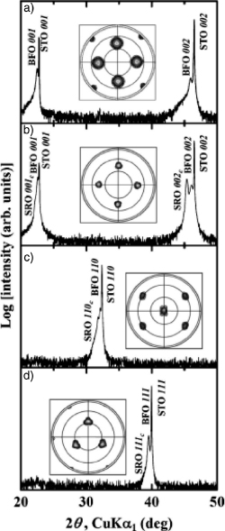
CSD method has been widely used in the preparation of BFO thin films, especially for seeking good dopants to improve the structural and electrical properties of BFO films [KIM 06, CHU 06, SIN 06, SIN 07, HU 07, MUR 08, IAK 05, UCH 06, LEE 07, SIM 07, LIU 08]. The following example helps us to understand the process details. For a typical preparation of Cr-doped BFO (BFCr) thin films, bismuth nitrate Bi(NO3)3•5H2O (5 mol % excess to compensate for Bi loss during high-temperature annealing) and chromium nitrate Cr(NO3)3•9H2O were dissolved in acetic acid at room temperature for 3 h using a stirring mixer. Then iron nitrate Fe(NO3)3•9H2O was dissolved into the stock solution, which was made from Bi–Cr. The precursor with a composition of BFCr was coated on p-type Si (100) substrates by the spin-coating technique at 3,500 rpm for 25 s. The silicon substrate, a boron-doped p-type Si (100) with a resistivity of about 1–10 Ω cm, was precleaned by HF solution (1:99 = HF/H2O) for 1 min. After each coating, the wet films were pyrolyzed at 350°C for 10 min over a hot plate. The coating and pyrolyzing processes were repeated several times to get the desired thickness. The coated thin films were crystallized at 550°C for 30 min in a nitrogen atmosphere. The crystalline structures of the thin films were analyzed by XRD analysis. It was demonstrated that the CSD-derived BFCr thin films were crystallized in a pure perovskite phase and had a rhombohedrally distorted structure [LEE 07]. It is noteworthy here that the epitaxial BFO thin films can also be fabricated by CSD. Singh et al. used CSD method to realize epitaxial BFO thin films with different orientations [SIN 06]. As depicted in Figure 12.6, the BFO films grown directly on SrTiO3 (STO) (001) and on SrRuO3 (SRO)-coated (001)-, (110)-, and (111)-oriented STO substrates show only the (00l), (110), and (111) peaks corresponding to the substrates without any secondary phase, demonstrating that the BFO films are well (001), (110), and (111) oriented along the normal to the substrate. The pole figure measurement confirms the cube-on-cube epitaxial relationship of BFO||SRO||STO, as shown in the inset of Figure 12.6.
Figure 12.6. θ–2θ x-ray diffraction patterns and pole figures (inset) of BFO films deposited by CSD on (a) (001)-oriented STO and SRO-coated STO with (b) (001), (c) (110), and (d) (111) orientations [SIN 06]
Similar to every other thin film deposition technique, CSD has its advantages and disadvantages [ROB 04]. The major advantages of the CSD technique are the relatively low investment costs of the technology and the excellent control of film composition on a molecular level through the control of the stoichiometry of the precursor solution. Other advantages include relative easy fabrication of films over large areas up to multiple square meters for dip and spray coating techniques and the compatibility with standard semiconductor-fabrication methods that offers a high throughput rate. On the other hand, the disadvantages of CSD include difficulty in the deposition of epitaxial films and ultrathin films (thicknesses < 30 nm) although the possibility has been demonstrated in selected systems. Another disadvantage of CSD is that the 3D structures with a high aspect ratio cannot be conformally coated.
12.2.3. RF magnetron sputtering
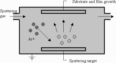
Magnetron sputtering is a powerful and flexible technique that can be used to coat virtually any workpiece with a wide range of materials — any solid metal or alloy and a variety of compounds. Sputtering is the removal of atomized material from a solid due to energetic bombardment of its surface layers by ions or neutral particles. The substrate is placed in a vacuum chamber with a target of the material to be deposited. Plasma is generated in a passive source gas (e.g. argon) in the chamber, and the ion bombardment is directed toward the target, causing the material to be sputtered off the target and condense on the chamber walls and the substrate. Figure 12.7 illustrates the working principle of sputter deposition. A strong magnetic field (magnetron) can be used to concentrate the plasma near the target to increase the deposition rate. RF power supply is used for the deposition of insulating materials.
Figure 12.7. Schematic illustration of the working principle of sputter deposition
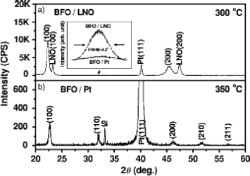
It is generally accepted that the electrical properties reported for multiferroic BFO thin films are largely dependent on the synthesis techniques and processing parameters involved. For example, considerable variation has been reported for both the polarization and leakage behaviors of BFO thin films. Therefore, it is of great interest to use the capability of RF magnetron sputtering in the preparation of BFO thin films. Interestingly, phase-pure BFO thin films have been prepared by RF magnetron sputtering on single-crystal SrTiO3 and Si-based substrates [DAS 06, LEE 06, YEH 08, LI 08, ZHE 07, CHA 09]. The realization of low-temperature growth of BFO thin films by RF magnetron sputtering is of particular interest. It was reported by Lee et al. that highly (100)-oriented BFO film was coherently grown on LaNiO3 (LNO)-buffered Pt/TiOx/SiO2/Si substrate at a temperature as low as 300°C [LEE 05]. In that work, the films were deposited by RF sputtering in a high vacuum system with a base pressure lower than 5 × 10⁻⁵ torr. The BFO films were grown on LNO/Pt/TiOx/SiO2/Si and Pt/TiOx/SiO2/Si substrates with a thickness of 200 nm. The target with a nominal composition of Bi1.1FeO3 was prepared by conventional ceramic procedures with reagent-grade oxide powders of Bi2O3 and Fe2O3. Figures 12.8a and 12.8b present the XRD patterns of the BFO films deposited on LNO and Pt, respectively. The crystallization temperature of the pure BFO perovskite phase was effectively reduced from 350°C (on Pt) to 300°C by the LaNiO3 electrode. Undoubtedly, such a low processing temperature is of great technological significance. Also interesting to note is that the BFO films are (100)-oriented and randomly oriented on LNO and Pt substrates, respectively, and the crystallinity of the film is greatly improved by the use of LaNiO3 electrode. It was proposed that compared with PLD and CSD methods, the low processing temperature of the BFO films by RF magnetron sputtering could be attributed to the increased mobility of surface atoms by energetically sputtered species.
Figure 12.8. XRD patterns of RF-sputtered BFO films deposited on (a) LNO and (b) Pt. The inset of (a) shows the rocking curves of BFO films deposited on LNO and Pt [LEE 05]
Typical advantages of RF magnetron sputtering include the following:
1) it is now quite a mature technique and has been widely employed in the semiconductor industry.
2) It is capable of preparing epitaxial films over large areas.
3) The technique itself is helpful in lowering the crystallization temperature of deposited thin films.
4) Sputtered films typically have very good adhesion on the substrate. However, the deposition rate is relatively low and the film composition is rather difficult to control for RF magnetron sputtering. Sputter deposited film might have a composition different from that of the source material.
12.3. Ferroelectricity and magnetism
12.3.1. Ferroelectricity
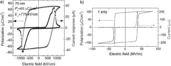
The ferroelectric polarization of bulk BiFeO3 is along the diagonals of the perovskite unit cell, i.e. [111]pseudocubic. Early measurements of bulk ferroelectricity in the 1960s and 1970s yielded only small values of the polarization (Pr ~ 6 μC/cm2). However, recently, it was argued that the small polarization values were caused by defects and are, thus, limited to lack of saturation; furthermore, high Pr values of about 60 μC/cm2 along the [001]pseudocubic direction were successfully obtained in good single-crystal BFO samples, which correspond to approximately 100 μC/cm2 along [111]pseudocubic [LEB 07]. Ab initio calculations also agree with the statement that the polarization of bulk BFO is intrinsically high, about 90–100 μC/cm2, and relatively insensitive to strain [NEA 05, EDE 05]. It is interesting to note that excellent ferroelectric properties can be similarly obtained in thin films of BiFeO3. For example, Pr values of 55 μC/cm2 along the [001] direction, of 80 μC/cm2 along the [101] direction, and of 100 μC/cm2 along the [111] direction were reported by Li et al. in epitaxial BFO thin films [LI 04]. Figure 12.9 shows √3P(001), √2P(101), and P(111) as a function of E for different oriented films. In this figure, the values of the projected polarizations can be seen to be nearly equivalent, ~100 μC/cm2. This confirms that the direction of spontaneous polarization lies close to (111), and that the values measured along (101) and (001) are simply projections onto these orientations. Importantly, it was reported by Yun et al. that polycrystalline BFO thin films deposited onto Pt/TiO2/SiO2/Si substrates could also show giant ferroelectric polarization [YUN 06]. As indicated in Figure 12.10, these polycrystalline BFO films show well-saturated rectangular-shape hysteresis characteristics and do not show evidence of leakage either at room the temperature or at 80 K. The ![]() values measured at room temperature and 80 K reach as high as 102 μC/cm2 and 152 μC/cm2, which are considered to be the highest among the so far measured values in ferroelectric materials. Nonetheless, a high leakage current, often observed in BFO thin films, might hinder a true measurement of the intrinsic ferroelectric polarization and limit their applicability in various electronic devices [PAB 07]. It has been proposed that the leakage in BFO could be effectively reduced through the addition of chemical dopants [CHU 06, UCH 06, QI 05] and in particular Mn dopant [ZHU 08, SIN 06, SIN 07]. Figure 12.11 shows the resistance maps for an undoped and an Mn-doped BFO thin films, both of which were measured over a 3 × 3 μm2 scan area on a 5 nm thick film with a conductive-tip atomic force microscope (CTAFM) [ZHU 08]. The results reveal that the Mn-doped BFO film is at a high resistance level (G Ω) with excellent homogeneity, and importantly, its resistance is much larger, by about 2 orders of magnitude, than that of the undoped film. This confirms that Mn dopant, indeed, reduced the leakage current in BFO thin films, thereby remarkably improving the intrinsic ferroelectric property measurements. Consequently, contrary to the difficulty in measurement of room temperature of intrinsic ferroelectric polarizations for pure BFO thin films, perfectly saturated P–E loops with hig Pr values have been obtained in both (001)- and (111)-oriented Mn-doped BFO films, as shown in Figure 12.12. The corresponding current responses help to understand the ferroelectric switching behavior better.
values measured at room temperature and 80 K reach as high as 102 μC/cm2 and 152 μC/cm2, which are considered to be the highest among the so far measured values in ferroelectric materials. Nonetheless, a high leakage current, often observed in BFO thin films, might hinder a true measurement of the intrinsic ferroelectric polarization and limit their applicability in various electronic devices [PAB 07]. It has been proposed that the leakage in BFO could be effectively reduced through the addition of chemical dopants [CHU 06, UCH 06, QI 05] and in particular Mn dopant [ZHU 08, SIN 06, SIN 07]. Figure 12.11 shows the resistance maps for an undoped and an Mn-doped BFO thin films, both of which were measured over a 3 × 3 μm2 scan area on a 5 nm thick film with a conductive-tip atomic force microscope (CTAFM) [ZHU 08]. The results reveal that the Mn-doped BFO film is at a high resistance level (G Ω) with excellent homogeneity, and importantly, its resistance is much larger, by about 2 orders of magnitude, than that of the undoped film. This confirms that Mn dopant, indeed, reduced the leakage current in BFO thin films, thereby remarkably improving the intrinsic ferroelectric property measurements. Consequently, contrary to the difficulty in measurement of room temperature of intrinsic ferroelectric polarizations for pure BFO thin films, perfectly saturated P–E loops with hig Pr values have been obtained in both (001)- and (111)-oriented Mn-doped BFO films, as shown in Figure 12.12. The corresponding current responses help to understand the ferroelectric switching behavior better.
Figure 12.9. P–E curves of (001)-, (101)-, and (111)-oriented BiFeO3 films, all of which were projected onto (111) plane [LI 04]
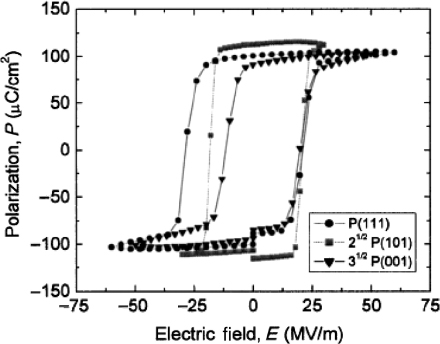
Figure 12.10. P–E hysteresis loops of polycrystalline BiFeO3 thin films deposited onto Pt/TiO2/SiO2/Si substrates measured at room temperature and 80 K [KWI 06]
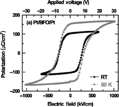
Figure 12.11. CTAFM resistance mappings for (a) 5 nm Mn-doped BFO film and (b) an undoped 5 nm BFO film, measured over 3 × 3 μm2 scan area and with the samples biased at 3 V. Note that the resistance of the Mn-doped film (Log R = 9.5 ± 0.2) is much larger than the undoped film (Log R = 7.2 ± 0.2) by roughly 2 orders of magnitude [ZHU 08]
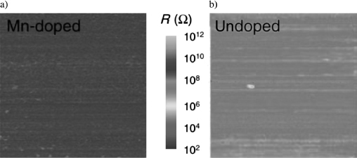
Figure 12.12. P–E hysteresis loops and corresponding electric field dependences of the current response for (a) (001)- and (b) (111)-oriented Mn-doped BFO thin films. The measurements were performed at the room temperature and at a frequency of 1 kHz [BÉA 08c, ZHU 08]
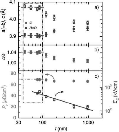
As mentioned earlier, the crystal class at ambient temperatures is rhombohedral for bulk BiFeO3. However, when BFO is epitaxially grown as a thin film onto, for example, a SrTiO3 (001) substrate, the resulting crystallographic morphology may be monoclinic, where the symmetry-lowering distortion arises from in-plane contraction and out-of-plane elongation as a result of lattice mismatch between film and substrate. In addition, there may be a further change in symmetry, from monoclinic to tetragonal, as the film thickness is reduced. Hence, there is a big debate over the film strain affecting the ferroelectric polarizations of BFO thin films. On the basis of the experimental fact that strain has a strong effect on the ferroelectricity of conventional perovskite films [CHO 04, HAE 04], the in-plane compression was initially thought to enhance the polarization in BFO thin films [WAN 03]. However, it is now known that this is not the case. Direct experimental proof of the small sensitivity of the polarization to the strain state was recently reported by Kim et al. [KIM 08], who demonstrated that the polarization of epitaxial BFO stays constant even as the epitaxial strain is relaxed with increasing film thickness, as depicted in Figure 12.13. A newer study about the relationship between strain and polarization in BFO has also been published by Jang et al., who confirmed that the spontaneous polarization does not change in absolute magnitude, but rather if can be rotated through the monoclinic symmetry plane [JAN 08]. The reason for the relatively small sensitivity to epitaxial strain in BFO is that its piezoelectric constant, which links strain to polarization, is relatively low (between 15 and 60 pm/V, compared to 100 and 1000 pm/V for other perovskite ferroelectrics) [CAT 09].
Figure 12.13. The absolute value of the ferroelectric polarization in BFO thin films (c) is essentially independent from in-plane compression of the films (a and b) [KIM 08]
It is worth mentioning here that the ferroelectricity endures in ultrathin BFO films with a thickness at least down to 2 nm, as demonstrated by piezoresponse force microscopy (PFM) observations in Figure 12.14 [BÉA 06c]. The clear contrast between the up and down stripes is related to the ferroelectric character of the 2 nm thick BFO thin film.
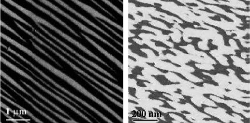
It is known that in rhombohedral BiFeO3, the ferroelectric polarization can point along any of the four diagonals of the perovskite unit cell with two antiparallel polarities for each direction; hence, there are eight different polar domains in BFO. There are three possible types of ferroelectric domain walls separating the adjacent domains, and these walls are usually labeled according to the angle formed between the polarization vectors on either side of the wall. When only one component of the diagonal polarization is reversed (say, one domain has [111] orientation and the adjacent orientation is [11-1]), the polar vectors form an angle of approximately 71° and the domain wall that separates the two polarizations is called a 71° wall. When two polar components are reversed, it is a 109° wall, and when all three components of the polarization are reversed, it is a 180° wall. Figure 12.15 schematically depicts these three types of ferroelectric domain walls, meaning that the direction of the polarization can be switched by 71°, 109°, and 180°. It should be pointed out that both stripe and mosaic domains (see Figure 12.16 for illustration) have been observed in thin films of BiFeO3. Domain walls have their own local symmetry and, hence, their own properties. Very interestingly, Seidel et al. have recently reported that certain domain walls of BiFeO3 are much more conductive than the domains themselves, which is called domain-wall conductivity [SEI 09]. It is suggested that the conductivity of the walls is directly related to the type of domains they separate. Accordingly, 180° walls are the most conductive, followed by 109° walls, and, finally, the 71° walls. The authors argued that there are at least two reasons for the enhanced conductivity of the domain walls. First, it is observed that the polarization normal to the domain wall is not constant across it; this generates an electrostatic depolarization field that may attract charge carriers. Second, the electronic bandgap is considerably reduced for the 180° and 109° domain walls. This new finding has great potential for novel nanoelectronic applications, as the domain wall location (and hence electronic conductive channels) can be precisely controlled on the nanoscale.
Figure 12.14. PFM images of 2 nm thick BFO thin films: (a) AFM topography, (b) PFM phase image of written up and down stripes, (c) horizontal domain written on (b), and (d) horizontal domain written on (c) with inverse polarization [BÉA 06c]
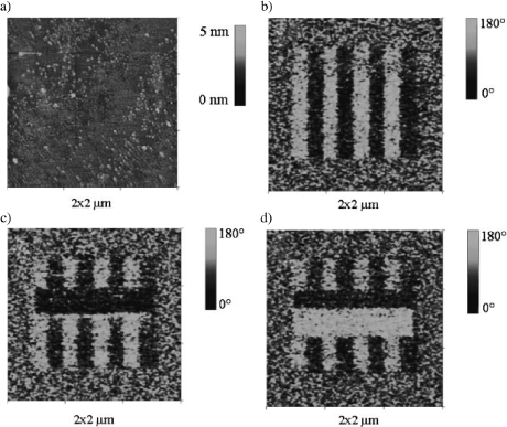
Figure 12.15. Schematic of the three types of ferroelectric domain walls separating domains with one, two, or all three components of the polarization switched. The domain walls are labeled according to the angle between the polarization vectors on either side [CAT 09]
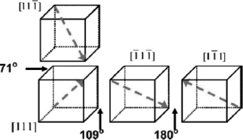
Figure 12.16. Ferroelectric stripe domains (left) and mosaic (also called “fractal”) domains (right) in epitaxial thin films of BiFeO3. The latter tends to appear only in very thin films [CAT 09]
12.3.2. Magnetism
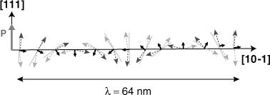
The local short-range magnetic ordering of BiFeO3 is a G-type antiferromagnet, that is, each Fe3+ spin is surrounded by six antiparallel spins on the nearest Fe neighbors. In fact, the spins are not perfectly antiparallel as there is a weak canting moment caused by the local magnetoelectric coupling to the polarization. Superimposed on this canting, however, is also a long-range superstructure consisting of an incommensurate spin cycloid of the antiferromagnetically ordered sublattices. The cycloid has a long repeat distance (wavelength) of 62–64 nm and a propagation vector along the [10-1] direction [LEB 08]. The magnetic easy plane (the plane within which the spins rotate) is then defined by the propagation vector and the polarization vector, as illustrated in Figure 12.17. Hence, in bulk BiFeO3, the weak local canting moment can be completely canceled by the averaging out effect of the cycloid, and the cycloidal spin modulation can also inhibit the observation of the linear ME effect, as discussed in the previous section. It is proposed that this cycloid structure may be partially destroyed by film strain and by reducing the sample size as small as the cycloid wavelength (~62 nm), leading to enhanced magnetization and ME coupling in thin-film or nanoscale BiFeO3 samples [WAN 09].
Figure 12.17. Schematic illustration of the antiferromagnetic circular cycloid. The canted antiferromagnetic spins (dotted arrows) give rise to a net magnetic moment (black arrows) that is spatially averaged out to zero due to the cycloidal rotation. The spins are contained within the plane defined by the polarization vector (along the [111] direction) and the cycloidal propagation vector (along the [10-1] direction) [LEB 08]
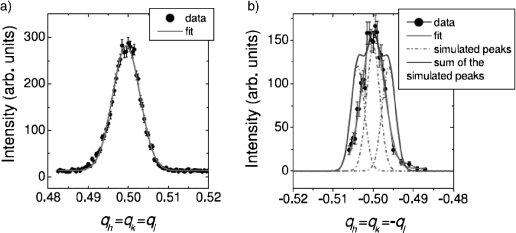
Bea et al. studied the magnetic order of BiFeO3 thin films by neutron diffraction [BÉA 07, BÉA 08d] and it is shown in Figure 12.18 that magnetic Bragg peaks (black data symbols) are clearly observed at ![]() and
and ![]() positions (* stands for reciprocal vector), indicating a G-type antiferromagnetic order, similar to bulk BFO. However, they emphasized that no satellites were observed around the
positions (* stands for reciprocal vector), indicating a G-type antiferromagnetic order, similar to bulk BFO. However, they emphasized that no satellites were observed around the ![]() Bragg peak, revealing that the spin cycloid is absent or that antiferromagnetic domains are too small for the cycloid to fully develop. They pointed out that if there were cycloidal modulation of spins, the presence of such a cycloid would considerably broaden the Bragg peak and satellites would be clearly visible, as displayed by the simulated peaks in Figure 12.18b. The absence of these satellite peaks in the experimental data indicates the absence of any bulk-like cycloidal modulation. In consequence, the absence of a full cycloidal modulation in the BFO films may allow the observation of the linear ME effect.
Bragg peak, revealing that the spin cycloid is absent or that antiferromagnetic domains are too small for the cycloid to fully develop. They pointed out that if there were cycloidal modulation of spins, the presence of such a cycloid would considerably broaden the Bragg peak and satellites would be clearly visible, as displayed by the simulated peaks in Figure 12.18b. The absence of these satellite peaks in the experimental data indicates the absence of any bulk-like cycloidal modulation. In consequence, the absence of a full cycloidal modulation in the BFO films may allow the observation of the linear ME effect.
Figure 12.18. Neutron diffraction patterns of ![]() and
and ![]() measured along the [111]* and [−1−11]* directions, respectively, for a 240 nm BFO film deposited onto SrTiO3 (001) [BÉA 08d]
measured along the [111]* and [−1−11]* directions, respectively, for a 240 nm BFO film deposited onto SrTiO3 (001) [BÉA 08d]
12.3.3 Magnetoelectric coupling
In bulk BiFeO3, the existence of a spin cycloid averages out any linear ME coupling between polarization (P) and magnetization (M). Any macroscopic ME coupling must, therefore, be of higher order (quadratic). Indeed, up to magnetic fields of several tesla, the magnetically induced polarization is found to be proportional to the square of the magnetic field (Figure 12.19a). Then, the full ME tensor (in hexagonal coordinate axis with P3 parallel to the spontaneous polarization) is given by [CAT 09]:
[12.4] 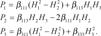
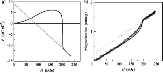
Above a certain critical field, ~20 T [POP 93, ZVE 06], however, the ME polarization changes sign and becomes linearly dependent on the magnetic field (Figure 12.19a), signaling a change in the spin configuration. Since the linear ME effect is forbidden by the cycloid, its onset signals that the cycloid has been destroyed by the high magnetic field. A second observation is that above the critical field for the cycloid destruction (or spin flop), the field-induced magnetization jumps to a higher value. Linear extrapolation of this field-induced magnetization to zero field yields a “remnant” magnetization of about 0.3 emu/g (Figure 12.19b). These effects can be understood theoretically as follows: the ferroelectric polarization breaks the center of symmetry and induces a small canting of the spins via the Dzyaloshinskii–Moriya interaction. This canting results in the very small magnetization of 0.3 emu/g. In addition, the ferroelectricity induces not only the canted magnetism but also the spin cycloid that averages out the local canted magnetism. This cycloid appears because polarization can also couple to gradients of magnetization (the spin cycloid). Although the cycloid averages out the macroscopic canting moment, it is locally still present at the unit-cell level. High magnetic fields can destroy the cycloid, thereby recovering the canted state and its associated remnant magnetization and, in this regard, the linear ME effect is allowed. It should be pointed out that the spin cycloid can also be destroyed by doping [WAN 05] or by epitaxial strain [BAI 05], so fully strained epitaxial thin films can, in principle, display a weak remnant magnetization.
Figure 12.19. Magnetoelectric effect in BiFeO3: (a) at low fields, P is proportional to H2 (quadratic ME coupling). Above BC = 20 T, P is linearly dependent on H instead. Since the linear ME is forbidden in the presence of a cycloid, the cycloid is destroyed above 20 T. Note that, in any case, the magnetically induced polarization is very small (roughly 105 times smaller than the ferroelectric polarization). Once the cycloid is destroyed, the small canted magnetic moment is recovered. (b) Extrapolation of the magnetization to zero field yields a small net magnetization of 0.3. emu/g [POP 93, ZVE 06]
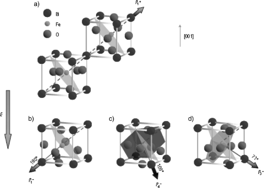
Specifically, it has been recently demonstrated in BiFeO3 single crystals that the magnetic moments rotate within the plane defined by the polarization (P//[111]pseudocubic) and the cycloid propagation vector (k//[10-1]pseudocubic) [88,92]. As presented in Figure 12.20, if the direction of the polarization is changed by, for example, applying a voltage and switching the polarization by 71°, the magnetic easy planes will be rotated correspondingly. It is important to note that the magnetic easy plane can be switched only if the polarization changes direction, but not if it merely changes polarity; i.e. 180° switching of the polarization should not affect the magnetic orientation. Interestingly, Zhao et al. reported a similar ME coupling phenomenon in thin films of BiFeO3 (Figure 12.21) [ZHA 06]. The thin films had no spin cycloid (due to either strain or reduced thickness), and instead they had the homogeneous G-type antiferromagnetism with a slight canting. The orientation of the antiferromagnetic sublattice magnetization, therefore, seems to be coupled to the ferroelastic strain state of the system and should always be perpendicular to the ferroelectric polarization. Using a combination of PFM and x-ray photoemission electron microscopy, the authors have managed to visualize simultaneously the ferroelectric and the antiferromagnetic domains, demonstrating that both types of domains are completely correlated with each other. Note that a coupling between antiferromagnetic and ferroelectric domains in BFO thin films has also been experimentally demonstrated by Béa et al. [BÉA 08a ] and Catalan et al. [CAT 08]. Moreover, switching the polarization by either 71° or 109° changes the orientation of the easy magnetization plane. This electrically induced switching of the magnetic easy plane, i.e. ferroelectric control of magnetism in BFO thin films is of great technological significance as it opens the door to fabrication of ME devices based on the voltage control of magnetization.
Figure 12.20. Relationship between the magnetic easy plane containing the spins, the vector of ferroelectric polarization, and the vector of cycloid propagation. Rotating the polarization by 71° results in a change of the magnetic easy plane, meaning that sublattice magnetization can be switched by an applied voltage [LEB 08]
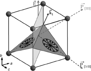
Figure 12.21. Schematic diagram of (001)-oriented BiFeO3 crystal structure and the ferroelectric polarization (bold arrows) and antiferromagnetic plane (shaded planes). (a) Polarization with an up out-of-plane component before electrical poling. (b) 180°polarization switching mechanism with the out-of-plane component switched down by an external electrical field. The antiferromagnetic plane does not change with the 180° ferroelectric polarization switching. (c) 109°and (d) 71°polarization switching mechanisms, with the out-of-plane component switched down by an external electrical field. The antiferromagnetic plane changes from the light gray plane to the black and dark gray planes on 109°and 71° polarization switching, respectively [ZHA 06]
12.4. Device applications
12.4.1. Non-volatile ferroelectric memories
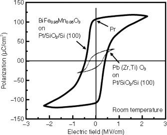
The remnant polarization of BiFeO3 is very large, ~100 μC/cm2, along the polar [111] direction. This is the largest switchable polarization among all perovskite ferroelectrics and is much larger than the polarization of the most widely used material in ferroelectric memories, Pb(Zr,Ti)O3 (PZT). A comparison of ferroelectric polarization between BFO and PZT is given in Figure 12.22. Moreover, unlike PZT, BFO is a lead-free material, which is a very important concern for environment, health, and safety. Therefore, BiFeO3 is considered a potential active material in the next-generation ferroelectric memory devices. Ferroelectric random access memory (FRAM, also called FeRAM) devices are non-volatile memories based on an electrical polarization phenomenon, whereby a charge and, thus, the stored information can be retained even without an externally applied voltage [SCO 00]. Fujitsu has recently announced the development of 65 nm ferroelectric random access memory devices using an Mn-doped BFO thin-film capacitor [FUJ 06]. For commercialization of FRAMs using BFO films, however, some important problems must be solved:
1) the high conductivity (and thus also dielectric losses) of BFO must be reduced;
2) its high tendency to fatigue must be decreased;
3) the high coercive electric field of BFO must be reduced;
4) a low temperature deposition method compatible with microelectronic technology must be adopted; and
5) a passivation film must be selected to prevent Fe diffusion [MAR 07].
Figure 12.22. Hysteresis characteristics in Mn-doped BFO thin films grown on technologically desirable platinized silicon substrates. The Pr value obtained is much larger than that obtained in Pb(Zr,Ti)O3 [MAR 07]. Large remnant polarization is a prerequisite for high-performance FRAM device applications
12.4.2. Spintronics
Spintronics (a neologism meaning “spin transport electronics”), also known as magnetoelectronics, is an emerging, and very exciting, technology that exploits the intrinsic spin of the electron and its associated magnetic moment, in addition to its fundamental electronic charge, in solid-state devices. The incorporation of multiferroic materials in the field of spintronics should allow us to not only take advantage of both functionalities (ferromagnetism/antiferromagnetism and ferroelectricity) independently but also add new functionalities due to the coupling between the two orders. This ME coupling between magnetism and ferroelectricity opens the way to control of the polarization by a magnetic field or control of the magnetization by an electric field. Then, one of the most exciting electronics applications would be memories that can be written using a voltage and read using a magnetic field. Using a voltage for writing has at least four advantages:
1) this can be implemented in a solid-state circuit without mobile parts;
2) it has a low-energy requirement;
3) it is a high-speed data-writing process; and
4) the voltage requirements automatically scale down with thickness.
Reading the memory magnetically, on the other hand, has the advantage that it is a non-destructive readout process, unlike direct ferroelectric reading, which requires switching the polarization and, thus, is a destructive readout process.
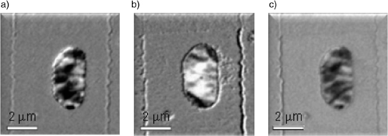
For such memories to actually work, the magnetic state, therefore, must be both electrically switchable and magnetically readable. The first condition is met by BiFeO3, because the easy plane of its antiferromagnetic domains is correlated with the polar direction, and rotating the ferroelectric polarization results in a rotation of the sublattice magnetization, as discussed in the previous section. This means that the magnetic state of BFO thin films can indeed be controlled by a voltage. On the other hand, the second condition is not directly met since antiferromagnetic (or, at best, weakly canted antiferromagnetic) domains cannot be easily read [CAT 09]. An elegant solution to this problem of reading antiferromagnetic states is the use of a mechanism known as exchange bias. The phenomenon of exchange bias consists of the offsetting and/or widening of the ferromagnetic hysteresis loops along the field in an antiferromagnetic/ferromagnetic system previously cooled under a magnetic field through the Néel temperature of the antiferromagnet [NOG 99]. Therefore, exchange bias is the magnetic interaction between the spins at an antiferromagnetic layer and a thin ferromagnetic layer attached to it. What is relevant here is that voltage-induced changes to the underlying antiferromagnetic domains will result in changes to the ferromagnetic hysteresis of the upper layer, which can then be read by conventional mechanisms. As far as BiFeO3 is concerned, there have been several important milestones reported in literature, such as the observation of exchange bias in thin ferromagnetic layers grown on BFO (Figure 12.23) [DHO 06, BÉA 08d], the correlation between exchange bias and ferroelectric domains [BÉA 08a], the observation that the antiferromagnetic domains can be switched by a voltage [ZHA 06], and the proof of concept that the exchange-biased ferromagnetic layer can indeed be switched by a voltage (Figure 12.24) [CHU 08]. It has been noted that the antiferromagnetic order in BiFeO3 can be exploited to modify the magnetization of a ferromagnet through exchange bias. In addition, due to the ME coupling effect, it may be anticipated that the manipulation of the antiferromagnetic order in BFO could result in controlling the magnetization of the exchange-biased ferromagnet with an electric field. This might, in turn, give rise to electrically writable spintronics devices such as spin valves or magnetic tunnel junctions, as will be discussed in the following paragraph.
Figure 12.23. Magnetic hysteresis loops measured at room temperature by using an alternating gradient force magnetometer for CoFeB (7.5 nm) layers deposited on (a) BFO (70 nm)/SrRuO3||SrTiO3 (001) and (b) BFO (70 nm)/SrRuO3||SrTiO3 (111)[BÉA 08d]
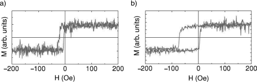
Figure 12.24. The magnetization of a small island of ferromagnetic Co–Fe is switched when a voltage is applied to the underlying BiFeO3 (white and black correspond to different magnetic polarities): (a) the as-grown state, (b) after the first electrical switch, and (c) after the second electrical switch [CHU 08]
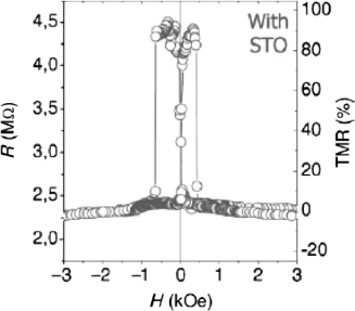
Using ultrathin BiFeO3 films as tunnel barriers in magnetic tunnel junctions is another interesting application of spintronics. Sandwiching BFO between two ferromagnetic metals results in tunneling magnetoresistance (TMR) (Figure 12.25) [BÉA 06d, BÉA 08d]. The TMR effect can be defined as a function of the resistance of the junction for the antiparallel (RAP) and the parallel (RP) states and of the spin polarizations (P1, P2) of the two ferromagnets:
[12.5] ![]()
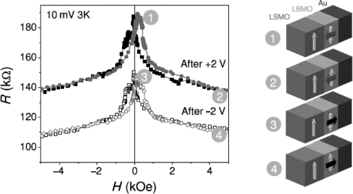
For this goal, the only requirement is that the BFO layer should be reasonably insulating down to tunneling thicknesses. Nonetheless, BiFeO3 being a multiferroic material, it provides an extra functionality that it also remains a robust and switchable ferroelectric down to a thickness of 2 nm [BÉA 06c], and thus it could, in principle, be used as an electrically switchable tunnel junction, namely, multifunctional tunnel junction, whereby the ferroelectric state controls the magnetic state of the thin ferromagnetic electrodes, thus modifying the TMR. As a matter of fact, this concept has been demonstrated by Gajek et al. [GAJ 07, BÉA 08d] using a ferromagnetic multiferroic (La0.1Bi0.9MnO3, abbreviated as LBMO). They showed that the tunneling resistivity could be controlled by both electric and magnetic fields, giving rise to a four-state memory device (Figure 12.26). More complex schemes have been proposed to store up to eight logic states in a single device [YAN 07].
Figure 12.25. Tunneling magnetoresistance (TMR) of BiFeO3 sandwiched between (La,Sr)MnO3 and Co [BÉA 08d], for which an ultrathin SrTiO3 (STO) protective layer was used before the BFO deposition. Note that a TMR up to +100% is obtained
Apart from the combination of ferroic properties in a single device, the electric control of magnetization by the ME coupling offers the opportunity of combining the respective advantages of FeRAMs and MRAMs (magnetic random access memories) in the form of non-volatile magnetic storage bits that are switched by an electric field. Indeed, although MRAMs show some superior characteristics in terms of access time and endurance compared to alternative non-volatile memory technologies, they have a big drawback in terms of their high writing energy. A possible solution that could dramatically reduce the writing energy of MRAMs is the use of a write scheme based on the application of a voltage. The ME coupling in multiferroics (e.g. BiFeO3) offers such an opportunity, giving rise to ME random access memories (MERAMs) [BIB 08]. Basically, MERAMs are operated by switching the magnetization of the ferromagnetic layer through the application of a voltage, which combines the ME coupling in multiferroic layer with the interfacial exchange coupling between a multiferroic and a ferromagnet (Figure 12.27). In other words, the ME coupling enables an electric field to control the exchange coupling at the interface of the multiferroic with the ferromagnet. The exchange coupling across the interface then controls the magnetization of the ferromagnetic layer, so that this magnetization can be ultimately switched by the electric polarization of the multiferroic and thus by a voltage.
Figure 12.26. Variations of the tunneling resistance of an Au/LBMO(2 nm)/LSMO junction with the magnetic field and previously applied electric bias, displaying four resistance states whose magnetic and electric configurations are presented on the right-hand side. Note that LSMO is referred to as (La,Sr)MnO3 [BÉA 08d]
12.4.3. Terahertz radiation
Takahashi et al. reported that when BiFeO3 films are hit with a femtosecond laser pulse, they emit THz radiation [TAK 06]. Currently, this is in the great interest of many applications ranging from telecommunications to security [RYZ 08]. Furthermore, the THz radiation is believed to be completely correlated with the poling state of the films (Figure 12.28). Therefore, THz emission could provide an ultrafast (picosecond response time) and non-destructive method for ferroelectric memory readout and a sensitive probe for ferroelectric domain imaging microscopy.
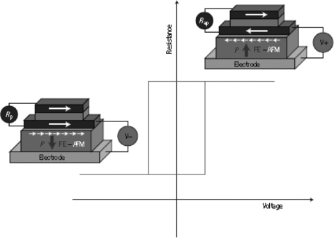
Figure 12.27. Sketch of a possible MERAM element. The binary information is stored by the magnetization direction of the bottom ferromagnetic layer (dark gray), read by the resistance of the magnetic trilayer (Rp when the magnetizations of the two ferromagnetic layers are parallel), and written by applying a voltage across the multiferroic (ferroelectricantiferromagnetic) layer (FE–AFM; mid-gray). If the magnetization of the bottom ferromagnetic layer is coupled to the spins in the multiferroic (small white arrows) and if the magnetoelectric coupling is strong enough, reversing the ferroelectric polarization P in the multiferroic changes the magnetic configuration in the trilayer from parallel to antiparallel, and the resistance from Rp to antiparallel (Rap) [BIB 08]. Interestingly, the multiferroic layer, for example, BFO, acts not only as the magnetoelectric active layer, but also as the antiferromagnetic layer for exchange coupling
12.4.4. Switchable ferroelectric diodes and photovoltaic devices
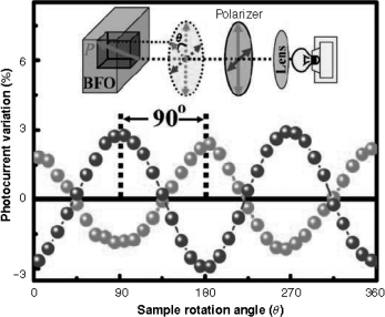
Unidirectional electric current flow in a diode is essential for modern electronics. It usually occurs at asymmetric interfaces such as p–n junctions or metal/ semiconductor interfaces with Schottky barriers. Very recently, a polarizationcontrolled diode effect and large photovoltaic currents have also been observed by Choi et al. in BiFeO3, a ferroelectric with a small optical gap edge of ~2.2 eV [CHO 09]. Figure 12.29a shows linear-scale J(E) curves of a thin plate-like BFO crystal at 300 and 350 K, which show diode-like behavior. For the typical p–n junction diodes, the forward current density follows an exponential relationship with applied voltage given by J α exp(qV/αkBT), where q is the electron charge, V voltage, α a constant called the ideality factor, and kB the Boltzmann constant. In the range of 0.05–0.15 kV/cm forward bias, α is 6.3 at 300 K and 4.7 at 350 K, much larger than the ideal value of 1 in semiconductor p–n junctions. It is also found that J increases drastically with the increase of temperature from 200 to 350 K as evident in the semi-log plot of J(E) curves in the inset of Figure 12.29a. In addition, the asymmetry in the J(E) curve also increases with increasing T. The rectification ratios, defined as the ratios of the positive current divided by the negative current for E = ±1.3 kV/cm, at 200, 250, 300, and 350 K, are 13, 159, 488, and 495, respectively. It is also interesting to note that the diode forward and reverse directions switch when ferroelectric polarization is uniformly reversed by large electric voltage pulses and the diode forward direction is always along the direction of ferroelectric polarization, as shown in Figure 12.29b. Associated with the diode effect is a substantial zero-bias photovoltaic current that is induced by visible light, and it is verified that the photovoltaic effect can be substantially affected by the light polarization (Figure 12.30).
Figure 12.28. (a) Experimental setup used by Takahashi et al. for measuring the THz emission of BiFeO3 (LT: low temperature; LSAT: LaAlO3-Sr2AlTaO6). (b) Time-domain waveform of the THz pulse radiated from the BiFeO3 photoconductive switch measured at a zero-bias electric field after applying a bias electric field Ebias of ±200 kV/cm. (c) Fourier-transformed amplitude spectrum of the waveforms in (b). The two THz waveforms are nearly identical, both consisting of a single-cycle pulse centered at 0 ps with a pulse width of about 0.84 ps, except that they have a reversed phase of π with each other. This definitely represents a ferroelectric peculiarity of a memory effect [KOU 06]
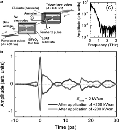
Figure 12.29. (a) J(E) curve of a symmetric Au/BFO/Au structure in the dark at 300 and 350 K. A substantial diode-like effect is evident. The inset shows semi-log-scale J(E) curves at various temperatures. All J(E) measurements were performed by sweeping the voltage from the positive maximum to the negative maximum in vacuum at 200–350 K. The applied electric fields are far below the coercive field for polarization switching. (b) J(E) curves of BiFeO3 after +150 V, −150 V, and +150 V pulses, in sequence. The diode forward and reverse directions switch when the direction of out-of-plane polarization (P) is reversed by ±150 V pulses. The diode forward direction turns out to be the same as the direction of electric pulses used for polarization flipping [CHO 09]
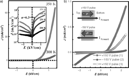
Figure 12.30. The variation of photocurrent with BFO sample rotation under illumination with a linearly polarized light. The experimental sketch is shown in the inset. The photovoltaic effect becomes maximum when the polarized-light electric field is parallel to the in-plane component of the ferroelectric polarization and becomes minimum when the field is perpendicular to the in-plane component [CHO 09]
There is no doubt that this finding is of great importance as it can improve the understanding of charge conduction mechanisms in leaky ferroelectrics and advance the design of novel switchable devices combining ferroelectric, semiconducting, and optical functionalities of BiFeO3.
12.5. Bibliography
[BAI 05] BAI F., WANG J., WUTTIG M., LI J.F., WANG N., PYATAKOV A.P., ZVEZDIN A.K., CROSS L.E., VIEHLAND D., Applied Physics Letters, vol. 86, p. 032511, 2005.
[BAR 07] BARK C.W., RYU S., KOO Y.M., JANG H.M., YOUN H.S.., Applied Physics Letters, vol. 90, p. 022902, 2007.
[BÉA 05] BéA H., BIBES M., BARTHéLéMY A., BOUZEHOUANE K., JACQUET E., KHODAN A., CONTOUR J.P., FUSIL S., WYCZISK F., FORGET A., LEBEUGLE D., COLSON D., VIRET M., Applied Physics Letters, vol. 87, p. 072508, 2005.
[BÉA 06a] BéA H., BIBES M., FUSIL S., BOUZEHOUANE K., JACQUET E., RODE K., BENCOK P. BARTHéLéMY A., Physical Review B, vol. 74, p. 020101(R), 2006.
[BÉA 06b] BéA H., BIBES M., SIRENA M., HERRANZ G., BOUZEHOUANE K., JACQUET E., FUSIL S., PARUCH P., DAWBER M., CONTOUR J.P., BARTHéLéMY A., Applied Physics Letters, vol. 88, p. 062502, 2006.
[BÉA 06c] BéA H., FUSIL S., BOUZEHOUANE K., BIBES M., SIRENA M., HERRANZ G., JACQUET E., CONTOUR J.P., BARTHéLéMY A., Japanese Journal of Applied Physics, vol. 45, p. L187, 2006.
[BÉA 06d] BéA H., BIBES M., CHERIFI S., NOLTING F., WAROT-FONROSE B., FUSIL S., HERRANZ G., DERANLOT C., JACQUET E., BOUZEHOUANE K., BARTHéLéMY A., Applied Physics Letters, vol. 89, p. 242114, 2006.
[BÉA 07] BéA H., BIBES M., PETIT S., KREISEL J., BARTHéLéMY A., Philosophical Magazine Letters, vol. 87, p. 165, 2007.
[BÉA 08a] BéA H., BIBES M., OTT F., DUPé B., ZHU X.H., PETIT S., FUSIL S., DERANLOT C, BOUZEHOUANE K., BARTHéLéMY A., Physical Review Letters, vol. 100, p. 017204, 2008.
[BÉA 08b] BéA H., BIBES M., HERRANZ G., ZHU X.H., FUSIL S., BOUZEHOUANE K, JACQUET E., DERANLOT C., BARTHéLéMY A., IEEE Transactions on Magnetics, vol. 44, p. 1941, 2008.
[BÉA 08c] BéA H., BIBES M., ZHU X.H., FUSIL S., BOUZEHOUANE K., PETIT S., KREISEL J, BARTHéLéMY A., Applied Physics Letters, IEEE Transactions on Magnetics, vol. 93, p. 072901, 2008.
[BÉA 08d] BéA H., GAJEK M., BIBES M., BARTHéLéMY A., Journal of Physics: Condensed Matter, vol. 20, p. 434221, 2008.
[BÉA 09] BéA H., DUPé B., FUSIL S., MATTANA R., JACQUET E., WAROT-FONROSE B., WILHELM F., ROGALEV A., PETIT S., CROS V., ANANE A., PETROFF F., BOUZEHOUANE K., GENESTE G., DKHIL B., LISENKOV S., PONOMAREVA I., BELLAICHE L., BIBES M., BARTHéLéMY A., Physical Review Letters, vol. 102, p. 217603, 2009.
[BIB 08] BIBES M., BARTHéLéMY A., Nature Materials, vol. 7, p. 425, 2008.
[CAT 08] CATALAN G., BéA H., FUSIL S., BIBES M., PARUCH P., BARTHéLéMY A., Scott J.F, Physical Review Letters, vol. 100, p. 027602, 2008.
[CAT 09] CATALAN G., SCOTT J.F., Advanced Materials, vol. 21, p. 2463, 2009.
[CHA 09] CHA J.O., AHN J.S., LEE K.B., Journal of the Korean Physical Society, vol. 54, p. 844, 2009.
[CHE 08] CHENG Z., WANG X., DOU S., KIMURA H., OZAWA K., Physical Review B, vol. 77, p. 092101, 2008.
[CHE 09] CHEN Y.C., LIN Q.R., CHU Y.H., Applied Physics Letters, vol. 94, p. 122908, 2009.
[CHO 04] CHOI K.J., BIEGALSKI M., LI Y.L., SHARAN A., SCHUBERT J., UECKER R., REICHE P., CHEN Y.B., PAN X.Q., GOPALAN V., CHEN L.Q., SCHLOM D.G., EOM C.B., Science, vol. 306, p. 1005, 2004.
[CHO 09] CHOI T., LEE S., CHOI Y.J., KIRYUKHIN V., CHEONG S.W., Science, vol. 324, p. 63, 2009.
[CHR 94] CHRISEY D.B., HUBBLER G.K., Pulsed Laser Deposition of Thin Films, John Wiley and Sons, Inc., New York, 1994.
[CHU 06] CHUNG C.-F., LIN J.-P., WU J.-M., Applied Physics Letters, vol. 88, p. 242909, 2006.
[CHU 08] CHU Y.H., MARTIN L.W., HOLCOMB M.B., GAJEK M., HAN S. J., HE Q., BALKE N, YANG C.H., LEE D., HU W., ZHAN Q., YANG P.L., Fraile-Rodríguez A., Scholl A., Wang S.X., Ramesh R., Nature Materials, vol. 7, p. 478, 2008.
[CRU 07] CRUZ M.P., CHU Y.H., ZHANG J.X., YANG P.L., ZAVALICHE F., HE Q., SHAFER P, CHEN L.Q., RAMESH R., Physical Review Letters, vol. 99, p. 217601, 2007.
[DAS 06] DAS R.R., KIM D.M., BAEK S.H., EOM C.B., ZAVALICHE F., YANG S.Y, RAMESH R., CHEN Y.B., PAN X.Q., KE X., RZCHOWSKI M.S., STREIFFER S.K., Applied Physics Letters, vol. 88, p. 242904, 2006.
[DHO 06] DHO J., Qi X., KIM H., MACMANUS-DRISCOLL J.L., BLAMIRE M.G., Advanced Materials, vol. 18, p. 1445, 2006.
[EDE 05] EDERER C., SPALDIN N.A., Physical Review B, vol. 71, p. 060401(R), 2005.
[EDE 05] EDERER C., SPALDIN N.A., Physical Review Letters, vol. 95, p. 257601, 2005.
[EER 05] EERENSTEIN W., MORRISON F.D., DHO J., BLAMIRE M.G., SCOTT J.F., MATHUR N.D., Science, vol. 307, p. 1203a, 2005.
[EER 06] EERENSTEIN W., MATHUR N.D., SCOTT J.F., Nature, vol. 442, p. 759, 2006.
[FIE 05] FIEBIG M., Journal of Physics. D: Applied Physics, vol. 38, p. R123, 2005.
[FIS 80] FISCHER P., POLOMSKA M., SOSNOWSKA I., SZYMANSKI M., Journal of Physics C, vol. 13, p. 1931, 1980.
[FUJ 06] FUJITSU MICROELECTRONICS AMERICA, INC., Sunnyvale, CA, Press Release, 2 August 2006 (http://www.fujitsu.com/ca/en/news/pr/fma_20060802.html).
[GAJ 07] GAJEK M., BIBES M., FUSIL S., BOUZEHOUANE K., FONTCUBERTA J., BARTHéLéMY A., Fert A., Nature Materials, vol. 6, p. 296, 2007.
[GAO 07] GAO F., CHEN X.Y., YIN K.B., DONG S., REN Z.F., YUAN F., ZOU Z.G., LIU J.M., Advanced Materials, vol. 19, p. 2889, 2007.
[HAE 04] HAENI J.H., IRVIN P., CHANG W., UECKER R., REICHE P., LI Y.L., CHOUDHURY S., TIAN W., HAWLEY M.E., CRAIGO B., TAGANTSEV A.K., PAN X.Q., STREIFFER S.K., CHEN L.Q., KIRCHOEFER S.W., LEVY J., SCHLOM D.G., Nature, vol. 430, p. 758, 2004.
[HU 07] HU G.D., CHENG X., WU W.B., YANG C.H., Applied Physics Letters, vol. 91, p. 232909, 2007.
[IAK 05] IAKOVLEV S., SOLTERBECK C.H., KUHNKE M., ES-SOUNI M., Journal of Applied Physics, vol. 97, p. 094901, 2005.
[IHL 07] IHLEFELD J.F., KUMAR A., GOPALAN V., SCHLOM D.G., CHEN Y.B., PAN X.Q., HEEG T., SCHUBERT J., KE X., SCHIFFER P., ORENSTEIN J., MARTIN L.W., CHU Y.H., RAMESH R., Applied Physics Letters, vol. 91, p. 071922, 2007.
[IHL 08] IHLEFELD J.F., PODRAZA N.J., LIU Z.K., RAI R.C., XU X., HEEG T., CHEN Y.B., LI J., COLLINS R.W., MUSFELDT J.L., PAN X.Q., SCHUBERT J., RAMESH R., SCHLOM D.G., Applied Physics Letters, vol. 92, p. 142908, 2008.
[JAN 08] JANG H.W., BAEK S.H., ORTIZ D., FOLKMAN C.M., DAS R.R., CHU Y.H., SHAFER P., ZHANG J.X., CHOUDHURY S., VAITHYANATHAN V., CHEN Y.B., FELKER D.A., BIEGALSKI M.D., RZCHOWSKI M.S., PAN X.Q., SCHLOM D.G., CHEN L.Q., RAMESH R., EOM C.B., Physical Review Letters, vol. 101, p. 107602, 2008.
[KAR 07] KARTAVTSEVA M.S., GORBENKO O. Yu., KAUL A.R., AKBASHEV A.R., MURZINA T.V., FUSIL S., BARTHéLéMY A., PAILLOUX F., Surface and Coating Technology, vol. 201, p. 9149, 2007.
[KHO 09] KHOMSKII D., Physics (APS), vol. 2, p. 20, 2009.
[KIM 06] KIM J.K., KIM S.S., KIM W.-J., BHALLA A.S., GUO R., Applied Physics Letters, vol. 88, p. 132901, 2006.
[KIM 08] KIM D.H., LEE H.N., BIEGALSKI M.D., CHRISTEN H.M., Applied Physics Letters, vol. 92, p. 012911, 2008.
[KUB 90] KUBEL F., SCHMID H., Acta Crystallographica B, vol. 46, p. 698, 1990.
[LEB 07] LEBEUGLE D., COLSON D., FORGET A., VIRET M., Applied Physics Letters, vol. 91, p. 022907, 2007.
[LEB 08] LEBEUGLE D., COLSON D., FORGET A., VIRET M., BATAILLE A.M., GUKASOV A., Physical Review Letters, vol. 100, p. 227602, 2008.
[LEE 05] LEE Y.-H., WU J.-M., CHUEH Y.-L., CHOU L.-J., Applied Physical Letters, vol. 87, p. 172901, 2005.
[LEE 06] LEE Y.-H., WU J.-M., LAI C.-H., Applied Physics Letters, vol. 88, p. 042903, 2006.
[LEE 07] LEE S.U., KIM S.S., JO H.K., PARK M.H., KIM J.W., BHALLA A.S., Journal of Applied Physics, vol. 102, p. 044107, 2007.
[LEE 08] LEE S., RATCLIFF W., CHEONG S.W., KIRYUKHIN V., Applied Physics Letters, vol. 92, p. 192906, 2008.
[LI 04] LI J., WANG J., WUTTIG M., RAMESH R., WANG N., RUETTE B., PYATAKOV A.P., ZVEZDIN A.K., VIEHLAND D., Applied Physical Letters, vol. 84, p. 5261, 2004.
[LI 08] LI Y., SRITHARAN T., ZHANG S., HE X., LIU Y., CHEN T., Applied Physics Letters, vol. 92, p. 132908, 2008.
[LIM 07] LIM S.H., MURAKAMI M., SARNEY W.L., REN S.Q., VARATHARAJAN A., NAGARAJAN V., FUJINO S., WUTTIG M., TAKEUCHI I., SALAMANCA-RIBA L.G., Advanced Functional Materials, vol. 17, p. 2594, 2007.
[LIU 06] LIU H., LIU Z., LIU Q., YAO K., Thin Solid Films, vol. 500, p. 105, 2006.
[LIU 08] LIU H., WANG X., Journal of Physics D: Applied Physics, vol. 41, p. 175411, 2008.
[LUO 07] LUO W.B., ZHU J., LI Y.R., WANG X.P., ZHAO D., XIONG J., ZHANG Y., Applied Physics Letters, Vol. 91, p. 082501, 2007.
[MAN 05] MANOJ K.S., SANGWOO R., HYUN M.J., Physical Review B, vol. 72, p. 132101, 2005.
[MAR 07] MARUYAMA K., KONDO M., SINGH S.K., ISHIWARA H., FUJITSU Science and Technical Journal, vol. 43, p. 502, 2007.
[MAZ 07] MAZUMDER R., SUJATHA D.P., BHATTACHARYA D., CHOUDHURY P., SEN A., RAJA M., Applied Physics Letters, vol. 91, p. 062510, 2007.
[MIC 69] MICHEL C., MOREAU J.M., ACHENBECHI G.D., GERSON R., JAMES W.J., Solid State Communications, vol. 7, p. 701, 1969.
[MOR 71] MOREAU J.M., MICHEL C., GERSON R., JAMES W.J., Journal of Physics and Chemistry of Solids, vol. 32, p. 1315, 1971.
[NAN 08] NAN C.W., BICHURIN M.I., DONG S., VIEHLAND D., SRINIVASAN G., Journal of Applied Physics, vol. 103, p. 031101, 2008.
[NEA 05] NEATON J.B., EDERER C., WAGHMARE U.V., SPALDIN N.A., RABE K.M., Physical Review B, vol. 71, p. 014113, 2005.
[NOG 99] NOGUES J., SCHULLER J., Journal of Magnetism And Magnetic Materials, vol. 192, p. 203, 1999.
[MUR 08] MURARI N.M., KUMAR A., ThOMAS R., KATIYAR R.S., Applied Physics Letters, vol. 92, p. 132904, 2008.
[PAB 07] PABST G.W., MARTIN L.W., CHU Y.H., RAMESH R., Applied Physics Letters, vol. 90, p. 072902, 2007.
[POP 93] POPOV Y.F., ZVEZDIN A.K., VOROBEV G.P., KADOMTSEVA A.M., MURASHEV V.A., RAKOV D.N., JETP Letters, vol. 57, p. 69, 1993.
[QI 05] QI X., DHO J., TOMOV R., BLAMIRE M.G., MACMANUS-DRISCOLL J.L., Applied Physics Letters, vol. 86, p. 062903, 2005.
[RAM 07] RAMESH R., SPALDIN N.A., Nature Materials, vol. 6, p. 21, 2007.
[RAN 07] RANA D.S., TAKAHASHI K., MAVANI K.R., KAWAYAMA I., MURAKAMI H., TONOUCHI M., YANAGIDA T., TANAKA H., KAWAI T., Physical Review B, vol. 75, p. 060405(R), 2007.
[ROB 97] ROBERT W.S., Chemistry of Materials, vol. 9, p. 2325, 1997.
[ROB 04] ROBERT W.S., THEODOR S., RAINER W., Comptes Rendus Chimie, vol. 7, p. 433, 2004.
[RYZ 08] RYZHII V., Journal of Physics: Condensed Matter, vol. 20, 380301, 2008.
[SCO 00] SCOTT J.F., Ferroelectric Memories, Springer, Berlin, 2000.
[SEI 09] SEIDEL J., MARTIN L.W., HE Q., ZHAN Q., CHU Y.H., ROTHER A., HAWKRIDGE M.E, MAKSYMOVYCH P., YU P., GAJEK M., BALKE N., KALININ S.V., GEMMING S., LICHTE H., WANG F., CATALAN G., SCOTT J.F., SPALDIN N.A., ORENSTEIN J., RAMESH R., Nature Materials, vol. 8, p. 229, 2009.
[SIM 07] SIMÕES A.Z., GONZALEZ A.H.M., CAVALCANTE L.S., RICCARDI C.S., LONGO E., VARELA J.A., Journal of Applied Physics, vol. 101, p. 074108, 2007.
[SIN 06] SINGH S.K., ISHIWARA H., MARUYAMA K., Applied Physics Letters, vol. 88, p. 162904 and p. 262908, 2006.
[SIN 07] SINGH S.K., MENOU N., FUNAKUBO H., MARUYAMA K., ISHIWARA H., Applied Physics Letters, vol. 90, p. 242914, 2007.
[SOS 82] SOSNOWSKA I., PETERLIN-NEUMAIER T., STREICHELE E., Journal of Physics C, vol. 15, p. 4835, 1982
[SPA 05] SPALDIN N.A., FIEBIG M., Science, vol. 309, p. 391, 2005.
[TAK 06] TAKAHASHI K., KIDA N., TONOUCHI M., Physical Review Letters, vol. 96, p. 117402, 2006.
[TER 06] TERNON C., THERY J., BARONS T., DUCros C., SANCHETTE F., KREISEL J., Thin Solid Films, vol. 515, p. 481, 2006.
[UCH 06] UCHIDA H., UENO R., FUNAKUBO H., KODA S., Journal of Applied Physics, vol. 100, p. 014106, 2006.
[UEN 05] UENO R., OKAURA S., FUNAKUBO H., SAITO K., Japanese Journal of Applied Physics, vol. 44, p. L1231, 2005.
[VAL 07] VALANT M., AXELSSON A.K., ALFORD N., Chemistry of Materials, vol. 19, p. 5431, 2007.
[WAN 03] WANG J., NEATON J.B., ZHENG H., NAGARAJAN V., OGALE S.B., LIU B, VIEHLAND D., VAITHYANATHAN V., SCHLOM D.G., WAGHMARE U.V., SPALDIN N.A., RABE K.M., WUTTIG M., RAMESH R., Science, vol. 299, p. 1719, 2003.
[WAN 04] WANG J., ZHENG H., MA Z., PRASERTCHOUNG S., WUTTIG M., DROOPAD R., YU J., EISENBEISER K., RAMESH R., Applied Physics Letters, vol. 85, p. 2574, 2004.
[WAN 05] WANG N., CHENG J., PYATAKOV A., ZVEZDIN A.K., LI J.F., CROSS L.E., VIEHLAND D., Physical Review B, vol. 72, p. 104434, 2005.
[WAN 06] WANG D.H., YAN L., ONG C.K., DU Y.W., Applied Physics Letters, vol. 89, p. 182905, 2006.
[WAN 09] WANG K.F., LIU J.M., REN Z.F., Advances in Physics, vol. 58, p. 321, 2009.
[YAN 07] YANG F., TANG M.H., YE Z., ZHOU Y.C., ZHENG X.J., TANG J.X., ZHANG J.J., HE J., Journal of Applied Physics, vol. 102, p. 044504, 2007.
[YEH 08] YEH C.-S., WU J.-M., Applied Physics Letters, vol. 93, p. 154101, 2008.
[YUN 06] YUN K.Y., RICINSCHI D., KANASHIMA T., M. OKUYAMA M., Applied Physics Letters, vol. 89, p. 192902, 2006.
[ZHA 06] ZHAO T., SCHOLL A., ZAVALICHE F., LEE K., BARRY M., DORAN A., CRUZ M.P, CHU Y.H., EDERER C., SPALDIN N.A., DAS R.R., KIM D.M., BAEK S.H., EOM C.B., RAMESH R., Nature Materials, vol. 5, p. 823, 2006.
[ZHA 09] ZHANG X.-Y., SONG Q., XU F., ONG C.K., Applied Physics Letters, vol. 94, p. 022907, 2009.
[ZHE 07] ZHENG R.Y., GAO X.S., ZHOU Z.H., WANG J., Journal of Applied Physics, vol. 101, p. 054104, 2007.
[ZHU 08] ZHU X.H., BéA H., BIBES M., FUSIL S., BOUZEHOUANE K., JACQUET E., BARTHéLéMY A., LEBEUGLE D., VIRET M., COLSON D., Applied Physics Letters, vol. 93, p. 082902, 2008.
1 Chapter written by Xiaohong ZHU.