
Spectroscopies combined with reflection high-energy electron diffraction (RHEED) for real-time in situ surface monitoring of thin film growth
Abstract:
The electron beam used for reflection high-energy electron diffraction (RHEED) can also be used for various surface analysis techniques such as X-ray emission spectroscopy (XES), total reflection angle X-ray spectroscopy (TRAXS), Auger electron spectroscopy (AES), cathodoluminescence (CL), and reflection electron energy loss spectroscopy (REELS). These techniques provide unique ways to perform in situ, during growth, monitoring of the surface atomic composition and chemical state. The basic electron–surface interactions and emission processes are described and the experimental techniques are presented. Typical examples of applications illustrate the capabilities of each technique and are compared in terms of information and experimental complexity with a special emphasis on their compatibility with large vacuum chambers and their challenging operating conditions.
Auger electron spectroscopy (AES)
reflection electron energy loss spectroscopy (REELS)
X-ray emission spectroscopy (XES)
7.1 Introduction
In addition to reflection high-energy electron diffraction (RHEED) observations, the high-energy electron beam offers unique capabilities for using several spectroscopic methods to provide valuable information about the elemental composition and the chemical environment of the growing surface. The techniques used presently are X-ray fluorescence spectroscopy (XRF) with a special, more surface-sensitive application, total refraction angle X-ray spectroscopy (TRAXS), Auger electron spectroscopy (AES), reflection electron energy loss spectroscopy (REELS), and, more limited to band structure analyses, cathodoluminescence (CL) spectroscopy. The aim of these applications is to gather additional information about the chemical composition of the surface layers. The primary interest is to measure in situ and during growth the composition of the material as given by the ratio of atomic concentrations. The composition of the surface itself may be different from that of deeper layers, especially at lower growth temperatures. The actual chemical composition of the surface during growth and how it correlates to the composition and quality of the grown material are also of interest and are especially important when using gas sources in order to find and to understand the adjustment of material flux and sample temperature.
The feasibility of in situ spectroscopy combined with RHEED in a growth chamber has a long history. Even in the 1970s, in the early stage of molecular beam epitoxy (MBE), X-ray detectors were added to growth chambers and provided unique material information. AES and X-ray photoelectron spectroscopy (XPS) were also implemented, giving more surface-specific information. Many combined devices have since been used, but these techniques remained isolated attempts and are not yet part of the standard basic tools to control the growth process.
The scope of this chapter is to describe the present status of the available spectroscopies, their potential developments in light of the information provided, and the development of new dedicated instruments. This chapter is restricted to spectroscopies combined with RHEED and used in situ and operated in real time during the growth process, in contrast to the experimental devices requiring an in situ sample transfer for analysis or requiring the interruption of the growth process during data acquisition. The most important need of in situ analyses is the quantitative measurement of atom concentration on and near the surface. When successful, these techniques are likely to become major tools for controlling the growth of compound materials.
Section 7.2 presents a short overview of the physical parameters involved for understanding the measured signals in terms of atomic densities and sample geometry. Section 7.3 is an overview of the present experimental set-ups and results. Section 7.4 compares results obtained by each technique and highlights developments expected in the near future.
7.2 Overview of processes and excitations by primary electrons in the surface
Fast primary electrons (PE) from the RHEED beam penetrate the surface and generate cascades of events in the near-surface region. These interactions or collisions are classified into elastic and inelastic scattering processes. Each process has a specific cross-section and an associated specific mean free path (MFP), corresponding to the average distance traveled between successive specific interactions. Most electrons penetrate the solid and undergo a large number of elastic scattering events with a wide range of deflection angles, leading to a zigzag path inside the crystal lattice. Figure 7.1(a) shows the impact of PE at normal incidence and Fig. 7.1(b) at grazing incidence. Many interactions are inelastic events that progressively reduce the kinetic energy of the PE until it occupies an energy level of the crystal band structure. Some trajectories will eventually bring electrons back toward the surface. They may leave the surface and be emitted with a wide distribution of kinetic energies, ranging up to the primary energy, and a wide angular distribution. They build the flux of backscattered electrons (BSE) leaving the surface. This BSE flux also interacts with the solid and increases the efficiency of the PE flux by creating additional excitations in the surface region. The BSE electron flux represents a major correction factor for quantification.
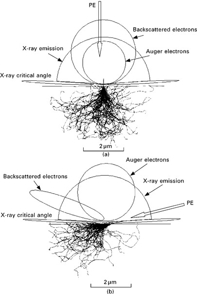
7.1 Trajectories of fast primary electrons inside the surface as calculated using a Monte Carlo computer simulation for (a) normal incidence angle and (b) grazing incidence angle. The angular distributions of backscattered electrons (BSE), Auger electrons, and X-rays emitted from the surface are also depicted.
7.2.1 Elastic scattering and elastic mean free path (EMFP)
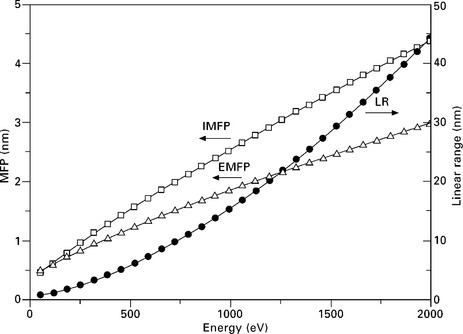
Elastic scattering is a process associated with large scattering angles with (almost) no energy loss (Murata, 1974; Reimer, 1985, p57). The elastic mean free path (EMFP) is the average distance traveled by the PE between two elastic scattering events and measures the strength of process. EMFP values for most elements and compounds have been calculated and are available as databases. Figure 7.2 shows the EMFP for silicon as function of the electron kinetic energy as tabulated from the database of Werner (2003, p235, 2010). Detailed understanding of the microscopic behavior of the PE is obtained using Monte Carlo computer simulations as shown in Fig. 7.1. The electron paths and spatial distribution of the electron near the surface becomes apparent and the distribution of the BSE flux can be accurately calculated, even at grazing incidence angles. Energy and angular distributions of BSE are in good agreement with experimental data (Ichimura and Shimizu, 1981; Ding et al., 2006). A recent program CASINO by Drouin et al. (2007), available for download from the web, allows customized calculation of the BSE factors for user specific geometries and materials. The calculated electron trajectories show how the BSE flux is the result of multiple small angle scattering events rather than one single large angle scattering event, as is the case for Bragg diffraction. There is the formation of a shower-like excitation volume under the surface. PE kinetic energy is progressively dissipated inside the excitation volume until the electron becomes part of the valence or conduction band.
7.2.2 Primary electron range and penetration depth
The range of primary electrons of kinetic energy Ep is a measure for the maximum penetration depth of the beam. It can be described, at normal incidence, using a simple power formula (Reimer, 1985, p96)
where a and n are material specific constants. The range R is expressed in μg cm−2. This relation is valid in an energy range 5–25 kV (Everhart and Hoff, 1971; Sogard, 1980). For Al or Si, the range is given by R = 4.0 Ep1.5 with E in kV. The range for Cu is given by R = 9.0 Ep1.5 showing that the energy variation of R is quite independent of the atomic number Z when measured as mass-thickness in units of μg cm−2. This range corresponds to the maximum penetration of the PE beam at normal incidence. The range in units of cm is obtained by the density ρ in g cm−3. More accurate calculations performed by Werner (2003) are available from the database (Werner, 2010). The range values, as shown in Fig. 7.2 for Si, are much larger than the EMFP or inelastic mean free path (IMFP).
7.2.3 Inelastic scattering processes and characteristic energy losses (CEL)
The PE can lose energy in several ways. The largest energy losses are the ionization of core energy levels and bremsstrahlung emission processes. Smaller loss values are related to plasmon and band excitation which are characteristic energy losses (CEL). Finally, small energy losses are due to phonon interactions and the creation of electron–hole pairs.
Inner shell ionization processes
The PE of energy Ep ejects an inner shell electron from an energy level Ei, leaving a vacancy in an inner shell energy level. The cross-section for this core level ionization process can be calculated using the formula given by Gryzinski (1965):
with G(Ui) a universal function depending only on the overvoltage parameter Ui = Ep/Ei. Ni is the number of electrons in the ionized shell. K shells contribute with two electrons and M45 shells with six electrons. Examples of calculated cross-sections as a function of the PE energy are shown in Fig. 7.3. The two major characteristics of the distributions are:
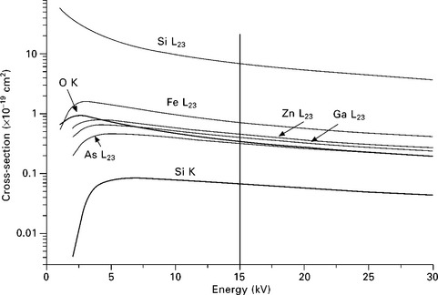
7.3 Ionization cross-sections for the K and L23 shell of selected elements as a function of the energy of the RHEED electron beam.
• The maximum cross-section for ionization is reached for primary electron energies 3 to 6 times larger than the ionization energy. For solids, the position of the maximum ionization yield is shifted toward higher PE energies because of the backscattered electrons as discussed below.
• The value of the maximum cross-section is larger for lower ionization energies Ei, as shown in Fig. 7.3 in the case of silicon. The cross-section at Ep = 15 keV for the low-energy L23 level (Ei = 104 eV, six electrons) is 100 times larger than for the K level (two electrons, Ei = 1844 eV). The difference in the values of the Si cross-sections is the dominant factor explaining the large variations of the signal intensities for different transitions in AES and X-ray emission spectroscopy (XES). On the other hand, the variation of σ for L23 shell ionization shows a weaker dependence on Z for neighboring elements like Fe to As for PE energies above 10 keV.
CEL: plasmons and band transitions
Electrons located in outer energy bands can be excited either as collective density oscillations known as plasmon excitation, or as single electron inter-and intra-band transitions. The result is the creation of CEL having a well-defined energy ΔE generally in the range from a few eV up to about 40 eV. The PE loses this amount of kinetic energy and is scattered by a small angle as required by the conservation of energy and momentum.
Plasmon losses correspond to the eigenmodes of resonance of the electron gas forming the outer electron shell, valence, and conduction bands. The plasmon frequency for a metal with an ideal free electron gas, like aluminum, is given by
with e the electron charge, m the effective mass of the electrons, and n the electron density of the conduction electrons (Raether, 1980; Ferguson, 1989). The excitation of plasmons is not restricted to free electron gas, but also exists for insulators and semiconductors because the plasmon energy, commonly in the range 5–30 eV, is larger than the electron binding or gap energy (Raether, 1980, p15). The plasmon loss energy is ΔE = ![]() ωp and is directly related to the density of state n and, therefore, to the chemical environment of the surface atoms. For instance, CEL of Al and Al2O3 are very different with plasmon loss energies of 15 and 23 eV respectively.
ωp and is directly related to the density of state n and, therefore, to the chemical environment of the surface atoms. For instance, CEL of Al and Al2O3 are very different with plasmon loss energies of 15 and 23 eV respectively.
Plasmon excitations come in two forms, surface and volume plasmons. The surface plasmon ωp,s corresponds to electron density fluctuations in the boundary surface and the loss energy is
for a free electron gas model. Plasmon losses are generally observed as multiple losses. The probability for an electron to suffer n plasmon losses depends on the ratio between the path length d traveled and the IMFP λ and is given by the Poisson distribution
as represented in Fig. 7.4. The no-loss probability P0 decreases very rapidly even for small values of d/λ. For d = λ, P0 is reduced by about 37% and equals P1, the first loss peak. Even a layer thickness of 0.5 nm will cause the no-loss peak to decrease to 60% of its value. This is a sensitive method for measuring the thickness of deposits like a gas adsorbed on the surface. The ratio between intensities of multiple plasmon losses can be compared to give an estimate of d/λ. A plasmon excitation can also occur during the ionization-recombination process (intrinsic excitation). An atomic layer adsorbed on the surface will suffer characteristic energy losses even if the escape distance traveled is negligible compared with the IMFP. This process adds to the excitation of extrinsic losses occurring during travel through surface layers.
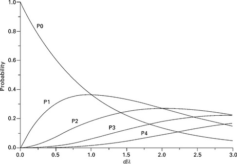
7.4 Probability for multiple energy loss as a function of the ratio between the path length d and the mean free path λ.
Band transitions are excitations of outer shell electrons. Ionization occurs when a valence or conduction electron is ejected, resulting in the creation of a vacancy. In contrast to optical absorption, the available momentum of the PE allows for direct and indirect band transitions. Band transition losses often occur in the same energy range as plasmons and overlap. The energy loss distribution is closely related to the optical properties of the surface. The energy loss function is given by the imaginary part of the complex dielectric constant (Raether, 1980, p35) and CEL distributions can be deduced from optical data. The strength of the energy losses is given by their IMFP which is the mean distance traveled by the electron between two CEL. The mean free path for a plasmon excitation is proportional to the electron kinetic energy, except in the low kinetic energy range (< 50 eV) where it increases. The IMFP shown for Si in Fig. 7.2 has a value of about 4 nm at 1800 eV and only 0.6 nm at about 100 eV. This is a large difference in escape depth for Auger or photoelectrons and is a major factor in the calculation of atom densities.
Continuous X-ray emission (bremsstrahlung)
Fast PE elastically scattered by nuclei in the crystal lattice are subject to strong acceleration and can emit X-ray photons of energy ranging up to the PE energy (Reimer, 1985, p158). The probability for this process is small and the process does not contribute significantly to the stopping power, but it generates a significant background continuum of X-rays. This background distribution adds to the characteristic X-ray lines and lowers the signal to noise ratio and the detection limit. The production rate Iv is given by Small et al. (1987)
with e the natural log base, Z the atomic number, and U = Ep/Ei the overvoltage parameter. The constants are M = 1.05 and B = 5.80 in the PE range 5 to 40 kV. The contribution increases almost linearly with Z and the detection of a low-Z element deposited on a high-Z substrate is more difficult than the other way around.
7.3 Recombination and emission processes
Core level vacancies created by fast PE impact are filled by electrons from higher shells and the energy is released either as X-ray photons or Auger electrons. The probability for the X-ray emission rather than an Auger electron emission is given by the fluorescence yield factor ω. Figure 7.5 shows the fluorescence yield for different shells plotted against the atomic number Z using data from Krause (1979) and Segre (MUCAL). The X-ray photon energy ranges up to several 10 keV, but the kinetic energy range of Auger electrons is much narrower. A range up to 2500 eV is sufficient to include the main Auger lines from all elements. The K shell Auger lines extend up to Z = 16 (S), the L shells up to Z = 46 (Rh), the M and N shells up to Z = 85 (At). These ranges are indicated in Fig. 7.5 and show that the fluorescence yields for the K, L, M shells are correspondingly low. For instance, the fluorescence yield for oxygen K is 0.83% and for silicon K is 5%. The fluorescence yields are small for low-energy transitions and Auger electron emission is the dominating process. Theoretical treatment of the Auger process is complex because of the existence of relaxation effects due to coulomb screening of the double ionized atom and possible interatomic cross-transitions (Coster–Kronig transitions). General descriptions of these emission processes are given in Reimer (1985) and Ferguson (1989) and are more detailed for XPS and AES applications in Briggs and Grant (2003).
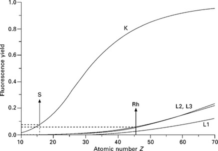
7.5 Fluorescence yields for the K and L shells as a function of the atomic number Z. The ranges corresponding to the KLL and LMM Auger transitions are marked and correspond to low fluorescence yield. After M.O. Krause and C. Segre.
Auger and characteristic X-ray lines generally have a multiplet structure. This structure can be resolved with a suitable energy resolution of the detector system. This is normally the case for AES energy analyzers and X-ray dispersive (XDS) spectrometers, with resolution in the range 1–5 eV. Energy dispersive X-ray detectors (EDS) have limited energy resolution, about 100–150 eV, and many fine structures will appear as a single peak.
7.3.1 Quantification of the signal intensities
The emission yield is primarily given by the cross-section for ionization, the escape depth, and the backscattering factor. The major experimental difference between XRF, AES, and REELS is the large difference in escape depth of photons or electrons. X-ray photons can escape from several micrometers below the surface whereas AE will be limited to a few nanometers. The absorption of X-rays is dominated by photo-ionization (mostly self-absorption) and Compton scattering. The resulting MFP value is in the range of several micrometers. In practice, the X-ray escape depth can be larger than the penetration of the PE beam for an energy of 10 keV. Most of the emitted X-ray photons generated near the surface are able to escape into vacuum and have a nearly isotropic angular distribution as shown in Fig. 7.1. The surface sensitivity of XES can be improved using grazing takeoff angles as discussed below for TRAXS. In contrast, the IMFP for Auger electrons is in the nanometer range (Ferguson, 1989, p25; Kanter, 1970) and the angular distribution more closely follows Lambert’s cosine law; see Fig. 7.1.
A convenient way to quantify the data is to use the ratio method based on reference spectra. Figure 7.6 shows the basic experimental conditions found in growth experiments. In the first case, Fig. 7.6(b), two elements A and B with atomic numbers ZA and ZB are forming an alloy A + B. The reference spectra from each pure element, corresponding to an atomic concentration of 100%, is measured and gives the signal intensities IA(100) and IB(100). An alloy of concentration x of A and 1 – x of B gives the signal intensities IA(x) and IB(1 – x). The signal intensity for the pure element A of volume density NA is given by
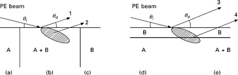
7.6 Models for calibration of atomic concentrations for a compound A + B (a, b, c), for a deposited layer A on B (d) and for a layer of B on A + B (e).
with σA the ionization cross-section for A for a PE beam of energy Ep and intensity Ip. MA is a correction for matrix effects that include multiple effects such as the backscattering coefficient, the fluorescence yield, and the escape probability of the particle to be emitted from the surface. The escape probability depends on the IMFP for Auger and REELS electrons or on the absorption for X-rays. It also depends on the angle of detection θA. The instrumental factor DA is the detection efficiency of the spectrometer for element A and includes the acceptance angle and transmission of the spectrometer. The detailed calculation of each correcting factor is complex and it can be simplified using reference data from pure elements. The ratio between the signals of an alloy of concentration x and the pure element is
The correcting factor is now the ratio between the matrix factor for the alloy MA(x), B(1 – x) to the pure element MA. The major variations are those of the attenuation length and backscattering factors, and the correcting factor can be expressed for a signal from A as
where dA is the escape depth of a signal from A at concentration x and 100% and BA is the backscattering factor for the same.
The second example is shown in Fig. 7.6(d) where element B is deposited on top of substrate A. Signal IB from element B will grow linearly at the beginning of the growth until the surface coverage reaches 1 ML (monolayer). For a thicker layer, IB will reach a steady value for deposits thicker than the escape depth of signal B in layer B. Concurrently, the signal A will decrease as the signal IA has to cross the layer B and finally will vanish. The absorption is characterized by the IMPF of IA through layer B and by the detector take-off angle θd. Signal IA will decrease as
with d the thickness (coverage) of B and λ the IMFP at the energy of line A in element B.
A frequent case is when growing a compound using a larger flux of one element, like As in GaAs or like O and O2 in oxide growth, where one element may accumulate on the surface. Figure 7.6(e) shows the case of the growth of element B on A + B where element B builds up on the surface. The signal IB comes from two contributions, one from the bulk and the other from the surface layer. IB will grow as long as the surface coverage remains low, below 1 ML, because the attenuation in layer B is small and both contributions can add. The signal from A will not change much. When the layer thickness is larger than the attenuation length λ, signal IB will saturate to its value for pure B material and signal A will vanish. Interestingly, in the case that the thickness is near λ and that the atomic number Z of A is larger than that of B (as for instance an oxygen layer on a metal oxide substrate), the IB signal will show a peak because the flux of BSE from A + B into the surface layer B is larger than the BSE flux from pure B. This example shows that the deduction of atomic densities from signal strengths requires the proper knowledge and modeling of the growth conditions on the surface.
7.4 Descriptions and results of in situ spectroscopies combined with reflection high-energy electron diffractio (RHEED)
This review focuses on recent combined techniques implemented in situ with RHEED and able to deliver results during the growth process, excluding analytical instruments built in situ but requiring sample transfer or interruption of the deposition process for acquisition of data. The environment of a growth chamber puts specific constraints on the instrument design in order to operate in situ and during growth.
• A large working distance between the sample and the detector system is required in order not to impair the atomic fluxes from the deposition sources.
• A good detection sensitivity allowing real-time data acquisition, fast enough to follow the growth process with acquisition times in the range 1–30 s is necessary for most processes.
• An outstanding resistance against material deposition is needed to ensure long-term stable operation over several months.
• The capability to operate in a wide range of pressures, from ultra-high vacuum (UHV) up to millitorrs, in order to be compatible with the operation of gaseous sources, is important.
Standard instruments are not directly suitable and must be modified to fit these applications. New instruments, specially designed for operation in growth chambers, are now being tested and will add new capabilities. The techniques presented here are CL, XRF, TRAXS, REELS, and AES.
7.4.1 In situ CL spectroscopy
CL is similar to photoluminescence (PL) spectroscopy because the recombination process is the same for both. There is, however, a major difference in the excitation process because, in the case of PL excited by a laser, the photon energy is fully absorbed, whereas electron excitation leads to a wide distribution of energy transferred. Further, the cross-sections for photon absorption have a peak at the transition threshold, but for electrons the increase is smooth near the threshold. PL can selectively excite specific transitions and CL will excite a wide range of transitions. The recombination process involves band transitions between the valence and conduction bands (Reimer, 1985, p289). Electrons from the valence band are excited into unoccupied states of the conduction band. A cascade of non-radiative phonon and electron excitations reduces their energy until they reach the bottom of the conduction band. The luminescence decay processes involve the creation of electron–hole pairs and excitons (Lightowlers, 1990). The transition can be direct or an indirect transition involving phonons in order to insure the conservation of momentum. The spatial extent of the region producing the CL signal is very large because all of the PE, BSE, and even most of the secondary electrons have sufficient energy to excite interband transitions and generate CL emission. The spatial area covers the full range of the cascade shown in Fig. 7.1. An additional broadening, due to the diffusion of the carriers during their lifetime before decay, further extends the emission volume (Reimer, 1985, p292). Therefore, the CL method basically delivers bulk information, except when observed transitions involve surface states.
Experimental set-up for CL spectroscopy
The CL set-up was developed for use in electron microscopes and involves the imaging of the beam spot through a large aperture optical collector (Reimer, 1985, p210). CL designs must be modified for in situ applications to accept larger sample size and to increase the clearance required between the sample and the optical system. In practice, only a limited beam aperture is focused onto the detector. In contrast with electron microscope chambers that are extremely dark, growth chambers contain various sources of stray light and in addition the sample may radiate when heated during the growth. Optical filters, adapted to the emitted CL spectral range can filter out the parasite light outside the CL emission range. A more efficient suppression method is the modulation of the PE beam intensity, using beam blanking, and measuring the signal using a lock-in amplifier detection technique (Lee and Myers, 2007).
Application of CL to the measurement of the substrate temperature
GaN having a direct band gap is a good CL emitter and the spectral distribution shows a peak energy corresponding to the band gap energy (Lee and Myers, 2007). The position of the maximum is very temperature sensitive. The peak shifts toward lower energy as the sample temperature increases. The temperature measured by CL represents the actual temperature of the very surface layer and represents a way to calibrate sample temperature between different chambers. Once calibrated, CL is able to detect variations of the surface temperature more precisely than the usual thermocouple measurement. CL provides a way to cross-calibrate temperature measured in different GaN growth chambers.
7.4.2 In situ XES combined with RHEED
XRF, also XES, is performed in situ using different detectors. One of the first experiments combining RHEED and XRF used a wavelength dispersive spectrometer (Sewell and Cohen, 1967). The wavelength dispersive spectrometer (WDS) is a windowless device and can detect low-energy X-ray lines, such as oxygen Kα. The energy resolution is sufficient to resolve the multiplet structure of the lines, but the major disadvantage is that the detected signal is low and the acquisition requires a long measuring time. More recent experiments use the EDS detector with the advantage of detecting all incoming X-ray photons and delivering a signal pulse with an amplitude proportional to the photon energy. Integration times are much shorter and compatible with the speed of growth of the surface. The energy resolution of the detector is, however, not as good as for the WDS system and lines of neighboring Z elements often strongly overlap.
Experimental set-up for RHEED-XRF in situ monitoring
The angular distribution of characteristic X-rays is basically isotropic (see Fig. 7.1), except in the range of very grazing angle of emission where the refraction effects become dominant. EDS detectors have a large sensitive area and accept radiation over a large solid angle. The acceptance solid angle must be reduced in order to block X-rays emitted from the chamber walls by X-ray fluorescence or BSE impact. A collimator system consisting of successive apertures is inserted between sample and detector. The Si(Li) detector crystal must be cooled in order to reduce the thermal background noise level. Cooling can use liquid nitrogen contained in a Dewar tank or, more simply, stacked Peltier cooling stages. Most detectors are sealed with a Be window in order to keep the crystal free of moisture condensation and contamination. In addition, the foil removes and blocks the light and BSE. Unfortunately, the Be window also acts as a filter absorbing the lower energy part of X-ray photons. The sensitivity of the detector is progressively reduced for photon energies below about 1 keV, cutting off, for instance, the oxygen Kα radiation. The Be foil can be replaced with lower Z materials, such as sapphire and C (in the form of polymer materials), or totally removed by carefully keeping the detector under controlled vacuum conditions. Because low Z window materials do not efficiently block fast BSE, a strong permanent magnetic can be used to dump the electrons before reaching the detector.
An additional requirement is to keep the detector crystal and the window foil free of material deposition. This is very important for quantitative analyses because any deposit will cause a nonlinear, selective absorption of X-rays and will selectively modify the intensities of measured peaks. A solution for materials with a low evaporation temperature is to use a heat control able to keep the foil clean during the process. This technique is used for elimination of the deposition of As during GaAs/AlGaAs by Pellegrino et al. (1998). Another approach is the use of an easily replaceable thin Be foil (Sun et al., 2009). In case the detector head cannot be easily accessed, moving a film like Mylar in front of the detector is another possible approach. Finally, X-ray energy dispersive detectors are not bakeable and must be placed far enough from the chamber wall or mounted on a mechanical retraction to move the detector far enough to stay at ambient temperature.
Quantification of characteristic X-ray line spectra
The signal intensity IA(x) of an element A is given by general Formula 7.7. The matrix factor is given by the product
of the fluorescence yield ωi for transition i, the backscattering factor B, the fluorescence factor F, and the attenuation length, corrected for the takeoff angle θd. The factor B becomes more significant when both incident and take off angles are small and is calculated by Monte Carlo simulations (CASINO). The standard method for quantitative calculation of atomic concentrations is described by Reimer (1985, p365) and referred to as the ZAF procedure. The method is based on the use of reference spectra from standards and followed by a linear combination of the standards to fit the measured signals. The accuracy of this simple method is much improved by introducing a correction factor for the Z dependence. It is assumed that the concentration is proportional to the ratio between the measured and the standard signal (corresponding to 100% concentration). Then the correction due to matrix effects, the ZAF factor, is introduced, taking into account variations of the BSE backscattering factor for different Z, of the absorption coefficient, and of the fluorescence factors between the actual sample and the standards. EDS-XRF combined with RHEED was used by Pellegrino et al. (1998) for quantitative monitoring of the surface composition of epitaxially grown InGaAs on GaAs. The stability of the signal over a long period of time is very reproducible and the accuracy of the mole fraction of In is < 0.1% after background correction. Quantitative analyses are performed by fitting Gaussian peaks for each element. The full width half maximum (FWHM) of the distribution is known to be the energy resolution of the detector and deconvolution of multiple, overlapping lines is therefore accurate and reliable (Hashimoto et al., 2009).
The surface sensitivity of EDS-XRF was tested by Ino et al. (1980) for the deposition of thin Ag layers on Si(111) surface. The detection limit is very good, less than 1% of a monolayer. The measurement of a high-Z material deposited on low-Z substrate is favorable for obtaining the highest detection limit because the bremsstrahlung background from the substrate is low and the PE backscattering and fluorescence effects are minimized.
7.4.3 Increasing the surface sensitivity with RHEED-TRAXS
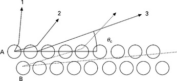
The signal in XRF is dominated by the bulk emission and has a limited surface sensitivity. When the take-off angle of the X-ray signal is limited to a small angular range very close to the surface plane, the X-ray signal becomes highly surface sensitive (Hasegawa et al., 1985). TRAXS is achieved when the geometrical conditions in Fig. 7.7 are fulfilled (Wang, 1996, p356). The X-rays emitted from a surface atom A at decreasing angle with the surface, labeled (1) and (2), are weakly refracted. The refractive index for X-rays is slightly smaller than unity and the emerging angle is larger than the incidence angle. X-rays emitted from A parallel to the surface (3) are refracted into vacuum at an angle θc. This angle is the critical angle for total refraction in XRF. Reversing the beam direction, X-rays with an incidence angle equal or smaller than θc will be totally reflected from the surface. There is no radiation emerging from the surface layer in the angular range between θc and the surface plane. The signal from deeper atomic layers B will not be emitted under the critical angle because the path to the surface is large and they will be absorbed. As absorption will cause fluorescence, a part of the signal from deeper layers may be re-emitted by the surface atoms, a process similar to the backscattering of electrons. The high surface sensitivity of this technique relies first on the small angular range selected by the detector close to the total reflection angle suppressing contributions from larger angles (and deeper layers) and second on the strong absorption of X-rays emitted at the critical angle but originating from deeper atomic layers. The depth of information is related to the decay length of the evanescent wave and is estimated in the order of 2 to 3 nm (Hasegawa et al., 1985).
Measurement of the critical angle in RHEED-TRAXS
The values for the critical angle are in the milliradian range and afford a high mechanical stability and accuracy of the positioning of the collimator unit. In principle, the take-off angle must be adjusted for each line when working under critical angle conditions. The critical angle for a compound is given by the simplified formula
for an X-ray of wavelength λ and a material of density ρ, mass number M, and atomic number Z. The critical angle depends both on the X-ray line energy and on the composition of the matrix. The angle is larger for lower X-ray energies (longer wavelength), for instance θc = 1.77° for Mg Kα (1254 eV) in MgO and only θc = 0.33° for Fe Kα (6403 eV) in BaFe12O19 (Sun et al., 2009). Accurate measurements of θc are given by Chandril et al. (2009) and Tompkins et al. (2006).
Measurement of layer thickness using attenuation by RHEED-TRAXS and in situ XPS
A different way to determine the thickness of a film during deposition is to measure the attenuation of a signal originating from the substrate. An example is given by Sun et al. (2009) for the deposition of MgO onto SiC. The relative intensity changes were observed under fixed RHEED electron energy (12.5 keV). Monitoring substrate Si Kα intensity decrease with film growth provides a real-time film thickness measurement. The film thickness is calibrated using in situ XPS measurements of the attenuation of the Si 2p3 photoelectron line at different angular incidence (angular resolved XPS).
Measurement of multilayer thickness using TRAXS and X-ray reflectivity
Chandrill et al. (2009) demonstrated that the angular dependence of XRF near the critical angle can be analyzed within the kinematic approach to yield useful structural information not only about a single thin film but also for a multilayered structure. Hence, it is possible to perform in situ quantitative structural characterization without the use of any reference samples. The X-ray reflectivity of a multilayer is measured ex situ using an X-ray beam of the same energy and scanned over the same angular range as the detected waves in TRAXS. This is like reversing the path of the X-ray waves and, according to the reciprocity theorem, the intensity of the X-rays emitted from a depth z inside a medium and observed at a grazing exit angle is proportional to the X-ray intensity, which is impinging at the same grazing incident angle and observed at the depth z inside the medium. Angular intensity profiles measured from multilayers of single layers of Mn and Y as well as bilayers containing Y on Mn and Mn on Y allow the determination of the layered structure and of the smoothness of the interface surfaces.
7.4.4 In situ reflection energy loss spectroscopy
Electron energy loss spectroscopy (EELS) is a familiar technique used in transmission electron microscopes for measuring the ionization losses suffered by the PE beam (Disko et al., 1992). The PE beam of high energy Ep (larger than 50 keV) is transmitted through a thin sample foil and is energy filtered by a high-energy resolution analyzer. The energy distribution of the transmitted electrons is measured and shows a strong direct transmitted peak at Ep of electrons transmitted with no energy loss. The intensity decreases very sharply with increasing loss energies and shows step-like structure corresponding to the ionization threshold energies Ei of core level electrons. As not only core level ionizations but also CEL losses like plasmons are possible, the observed step can be shifted by one or more plasmon energies depending on the IMFP for plasmon excitation and film thickness (Egerton, 1992, p41). The thickness of the sample is selected to optimize the ionization yield and to keep the plasmon losses to a minimum.
REELS is a similar technique that is used in reflection instead of transmission. There is a major difference between the transmission and reflection modes. In transmission and under optimal thickness conditions, the PE direct beam is straight and its angular extension is limited by the small analyzer acceptance angle (typically 50 milliradian). The ionization process leads to a smaller scattering angle, especially at larger PE kinetic energies, and is accepted by the filter whereas elastically scattered PE and BSE are rejected. In reflection mode and under RHEED conditions, the total scattering angle between the PE beam and detector is large. Elastic scattering collisions are needed to backscatter the PE beam and consequently it is mixed with the flux of BSE emerging from the surface. In contrast with the transmission mode, the ionization loss structures sit on top of a larger distribution of BSE (see Fig. 7.1). Unlike for the transmission mode, there is little latitude to optimize the length traveled by PE in the surface region in order to optimize the probability of excitation. The only factors which can be used are the incidence angle and the beam energy Ep. The signal to background ratio (S/B) is therefore not as good as in transmission mode.
Experimental set-up for REELS analyses
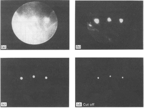
A modified TEM (transmission electron microscope) energy filter for energy losses spectroscopy is used in reflection mode by Nikzad et al. (1992). A small pencil of diffracted or diffused beam is selected and enters the analyzer. The beam is energy filtered by a stigmatic imaging magnetic sector followed by a set of magnifying projection lenses. The focal plane contains a range of energies which are collected simultaneously. Another analyzer for REELS is a device that combines energy filtering and imaging. The full diffraction diagram is accepted and, by means of a set of electron lenses, is energy filtered and projected onto a fluorescent screen similar to the usual RHEED screen (Staib et al., 1999). The angular distribution is preserved and RHEED diagrams are energy filtered as shown in Fig. 7.8. The filtering progressively removes the inelastic BSE part and, at the cut off energy Ep, only the elastic diffracted spots remain and energy losses are filtered out. REELS distributions are achieved by measuring the intensity of a selected area of the diffraction diagram and lowering the energy filter voltage from above the elastic peak down to a few 100 eV loss energy. The signal is measured using a lock-in detection technique in order to improve the signal to noise ratio.
Examples of in situ REELS distributions
The surface sensitivity of REELS is demonstrated by Nikzad et al. (1992) for the deposition of Ge onto Si. The growth of the Ge L23 ionization edge is recorded at a PE energy of 30 keV. A 0.15 nm deposited layer is clearly detected after normalization of the spectra. Weaker structures can be detected after differentiation of the signal. A more detailed discussion of REELS in MBE is given by Wang (1996, p334).
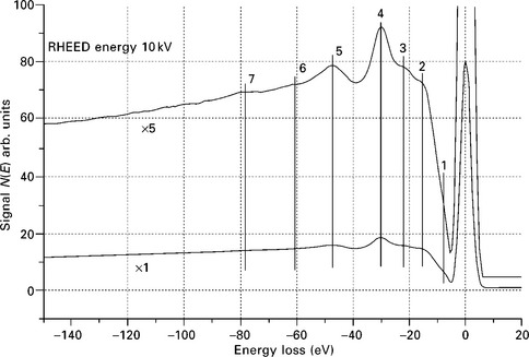
Figure 7.9 shows the REELS distribution of SrTiO3 recorded at Ep = 14.5 kV measured using the imaging energy filter described by Staib et al. (1999). The energy loss distribution includes the elastic peak and multiple CEL features. The losses are strongly apparent without background subtraction. The electron binding energy levels, available from Sevier (1972) and updated by Williams (2006), are used to identify the loss structures. The structures (6) correspond to Ti 3s (58.7 eV), (4) to Ti 3p1/2 3p3/2 (32.6 eV), (3) to Sr 4p1/2 (21.6 eV) and Sr 4p3/2 (20.1 eV). Loss energy (5) corresponds to O 2s (41.6 eV) but is shifted to about 47 eV as a result of a chemical shift.
Use of RHEED-REELS for monitoring the surface growth and roughness
The ratio between surface and volume plasmon is used to characterize, in situ during growth, the surface roughness of a deposited Al film on sapphire (Strawbridge et al., 2006). The layer thickness was calibrated ex situ by Rutherford backscattering (RBS) and the surface roughness was measured by atomic force microscopy (AFM). The change of the energy loss distribution from the bare sapphire substrate to deposited Al layer is very sensitive to the Al atomic concentration. For thin layer deposits, only the surface plasmon is observed. For larger deposits in the range 3–14 nm, two behaviors are found; either the surface plasmon remains dominant correlating to a smooth surface deposit, or the volume plasmon dominate witnessing a rougher surface as confirmed by AFM scanning images. It is worth noticing that RHEELS data can be acquired in spite of the fact that sapphire is an excellent insulator. RHEELS is far less sensitive to charging effects than other analysis methods because the gain or loss in kinetic energy of the PE due to the surface charges compensates after backscattering. The PE enters and leaves the surface within a nanometer scale offset and the surface potential is homogeneous over this range. The same holds for the characteristic energy and ionization losses.
Monitoring the ionization loss for quantitative analyses
Quantitative analyses can be performed using the technique developed for transmission EELS as described by Leapman (1992). The intensity of the EEL structures is measured after background subtraction using a simple power law formula. The signal is then integrated over an energy width that includes the CEL region. A similar calculation can be used for reflection EELS, but an additional correcting factor is needed to account for backscattering effects (which are not present in transmission). The extraction of structures near the elastic peak, where ionization losses are superimposed on multiple CEL losses, requires a Gaussian background fitting.
7.4.5 In situ monitoring by Auger electron spectroscopy (RHEED-AES)
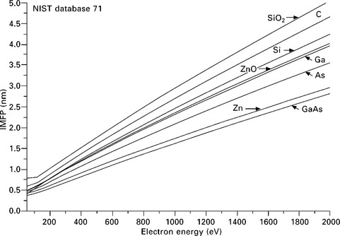
The escape depth of Auger electrons is given by the IMFP for a specific Auger line energy and material composition. A few relevant IMFP data are plotted in Fig. 7.10 as function of the kinetic energy using tabulated data from Powell (2000, NIST database 71). The plot shows that the IMFP depends on Z, but is even more dependent on the chemical state of the surface. Oxides like SiO2 and ZnO have larger IMFPs than their pure components. The MFP is minimum for kinetic electron energies in the range 30–50 eV with values around 0.5 nm and increases to values 2–3 nm at 1000 eV (Ferguson, 1989, p25; Tanuma, 2003). When working with very thin deposited or adsorbed layers, the IMFP can alternatively be expressed in terms of monolayer coverage.
Experimental set-up for RHEED-AES
For in situ operation, the energy analyzer must fulfill the specific requirements listed previously. These constraints rule out the classical spectrometer designs in favor of specially designed systems consisting of an electron optical lens system collecting the Auger electrons in front of the sample followed by an energy filter located further away from the sample, possibly behind the chamber wall. The angular position of the analyzer with respect to the surface is important. The analyzer should not be mounted at grazing take-off angle because the angular distribution of Auger electrons roughly follows Lambert’s law of a cosine distribution. The maximum peak intensity is normal to the sample surface; see Fig. 7.1. In contrast, the BSE peak toward the direction of specular reflection. Thus, an Auger analyzer mounted with its axis normal to the sample will collect most of the Auger electrons, less BSE, and thus have the best sensitivity. The normal position has the advantage of not being sensitive to crystalline channeling effects affecting the angular distribution of Auger electrons, especially marked for low energy lines. The azimuthal rotation of the sample during acquisition is then possible. An additional electron gun, positioned far from grazing incidence angle (about 45°) and able to work over a wide energy range, is useful for calibration purpose in quantitative analyses and for measuring REELS distributions in a lower beam energy range.
In situ monitoring of oxygen during ZnO oxide growth on GaN substrates
ZnO is grown on top of a GaN substrate using a radio frequency (RF) plasma source for oxygen deposition. The growth process can be followed in real time using a fast Auger probe analyzer mounted at normal incidence angle using the experimental set-up given by Staib (2011). The Auger electron lines of Ga LMM (1066 eV), oxygen O KLL (503 eV) and Zn LMM (990 eV) are monitored. The growth rate is about 10 ML/min and at an acquisition speed of 6 V/s, the measuring time for an Auger line is 3–10 s. The Ga signal abruptly vanishes and the Zn signal grows rapidly when the Zn shutter opens; see Fig. 7.11(a). The oxygen line is present on the surface, provided by the residual gas pressure in the chamber. The oxygen K LVV line grows further on opening the oxygen source shutter (see Fig. 7.11b), and reaches a stable value. The normalized intensity ratio of O KLL to Zn LMM is a measure of the ratio of atomic concentrations.
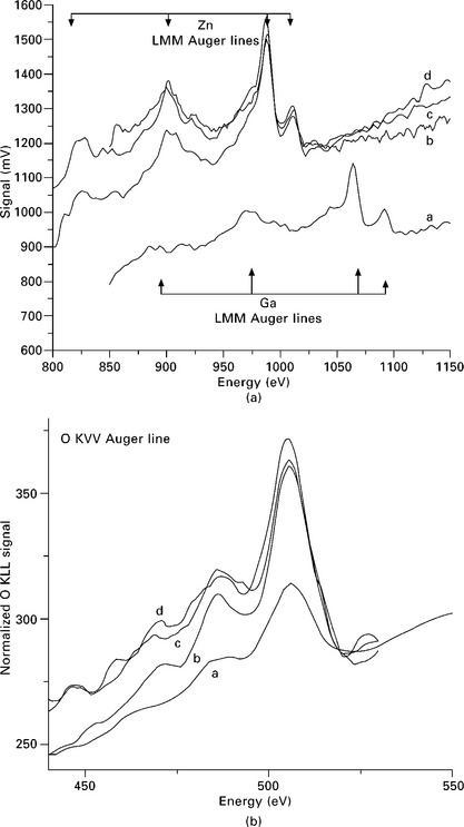
7.11 (a) Growth of ZnO on GaN substrate. The Ga LMM Auger line disappears as the Zn LMM line grows rapidly to a steady state value. (b) Growth of the oxygen O KLL Auger line under the same conditions. Curves labelled ′a′ correspond to the initial substrate, curves labelled ′d′ indicate the final state.
In situ monitoring of growth of MgO and of Crx Mo(1–x) on MgO substates
Chambers et al., (1996) used RHEED combined with AES and in situ XPS to study the homoepitaxy growth of MgO on Mg0(001) substrates. The sample temperature is kept at 750 °C during deposition and oxygen is provided by an electron cyclotron resonance (ECR) plasma source. The Auger lines of Mg KLL and O KLL are converted into atomic densities by cross-calibration using in situ XPS intensities of the Mg 2p and O 1s photoelectron lines. The atomic percentages of Mg and O remain constant at 50 ± 2% during the growth. Heteroepitaxy of Cr, Mo alloy films on MgO can have a wide range of composition controlled by the atom fluxes. The composition of the films is measured during growth by monitoring the intensity of the Cr LMM and Mo MNN Auger lines. The calibration is performed by measuring the signal of the pure elements Cr and Mo substrate and a linear interpolation (ratio method) is used to quickly determine the film composition. The results are in good agreement with in situ XPS calibrations.
In situ growth control of lanthanide alloys
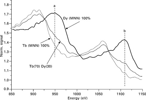
The Auger probe was used by Calley et al., (2011) to monitor the co-deposition of Fe, Dy and Tb on silicon substrates using the Auger spectrometer described by Staib (2011). The Auger spectra were measured at a primary beam energy of 10 kV and a beam current in the range of 3–10 μA. The intensities of the Dy and Tb MNN Auger peaks were much weaker than for the Fe lines because the Auger yield issued from the M shell ionization was distributed into a more complex multiplet structure extending over a wider energy range. The detection sensitivity was increased by using a lower energy resolution ΔE = 20 eV. The MNN lines shown in Fig. 7.12 correspond to pure Tb (100%) and pure Dy (100%). The quantification of the signals into atomic concentrations is possible using the peak heights, the area under the peaks, or the derivative signals and measuring the peak to peak amplitudes. These techniques are complicated in this example by the fact that the two Auger lines strongly overlap. The measured energy of an alloy Tb(70) Dy(30) is also shown. It shows that in spite of the overlap, there are energy regions marked by the lines a and b where the distributions vary markedly between the pure element. It is then possible to characterize a specific alloy composition calibrating the signals in this energy range as shown by Calley et al. (2011). A precision better than 2% for the atomic ratios could be demonstrated.
Chemical information from the Auger line shape and energy position
Auger lines provide multiple information about the composition and chemical state of the surface layer. All elements, except H, can be directly identified by their line energy and the concentration of elements can be deduced from the signal strength after calibration. In contrast with X-ray emission lines, the line shape and energy position can provide chemical information about the surface atoms.
The shape of the Auger lines provides useful information about the chemical environment and in-depth distribution of the elements as described by Ramaker (2003). The shape of the peak reflects the details of the transitions between core and valence-type band which depend on the density of states. In addition, the satellite structure of the Auger lines reflects the distribution of CEL that varies with the chemical environment of the atoms. The probability for the occurrence of a CEL depends on the position of the atom with respect to the surface. The line shape of atoms from deeper atomic layers show strong, multiple CEL structures, more visible in the N(E) mode than the dN(E)/dE mode. Auger peak energies are, in many cases, sensitive to the chemical bounding of the surface atoms. Chemical shifts, which are directly related to the changes in binding energy of core electron levels, are more common in XPS. Energy variations of an Auger peak are the result of transitions involving three energy levels which are all shifted by chemical bonding. In addition, the final state is a double ionized atom followed by a relaxation process as described by Grant (2003). The resulting shift is more complex than for XPS and some chemical bonding may not lead to noticeable energy shifts when all involved atomic levels are shifted by the same amount. However, a large number of chemical species result in changes in peak position and shape. The change in the energy of an Auger line was first accurately measured in XPS spectra. The chemical effects are measured using the energy difference between the Auger line and the photoemission line of the same element. The difference is constant if both lines shift with the same amount, but it will change if the Auger line shifts differently. The relation between the chemical shifts of the Auger and XPS peaks was described by Wagner (1972), introducing the notion of Auger parameters. A detailed description of the processes involved was given by Moretti (2003). A useful set of experimental data may be found in older AES reference books, such as from Wagner et al. (1979) and Moulder et al. (1992). The in situ during growth measurement of the Auger has a unique capability to show variations of chemical bonds of elements on the surface. An example of such behavior is given by Staib (2011) where the oxygen Auger peak shows a shoulder that corresponds to adsorbed oxygen on the surface and not incorporated into the oxide matrix.
The measurement of energy shifts can be complicated by the fact that the surface potential may vary as a result of charging up when the surface has a poor electrical conductivity. The energy position of the peak can be shifted by large amounts and, in a worst case, the signal becomes very unstable, making the measurement impossible. For moderate charging effects, the peaks will all be shifted by the same amount. The energy difference between peaks can then be used to measure the relative energy shifts between different Auger lines.
Control of the surface purity during the deposition process
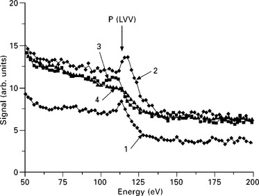
Control of the surface purity during the deposition process is the most common application of AES, an obvious application for monitoring the atomic purity of the deposited layer. The surface composition can be monitored during the growth process. Although the vacuum chamber and deposition sources are most carefully prepared, experience shows that unexpected materials can be deposited on the surface. Figure 7.13 shows the sudden appearance of a phosphorus line when starting a deposition source. The P impurity is soon buried during growth, but the electrical properties of the deposited layer are likely strongly modified. Similar observations have been made on carbon, oxygen and chlorine. The systematic use of AES during growth is a convenient way to guarantee the chemical integrity of the material. This monitoring may become an important tool in performing purity control in real time throughout the deposition process.
7.5 Conclusion and future trends
The different techniques available conjointly with RHEED have been presented. Fortunately, the RHEED electron beam with a grazing incidence angle enables all techniques to achieve higher emission yields and better surface sensitivity. The requirements for the incident beam are very similar for all diagnostics. A beam current adjustable in the range 100 nA to 10 μA is sufficient for almost all applications. The energy range can be limited to 5–30 keV for most applications, but lower energies in the range 1–5 keV are very useful to acquire REELS data with an AES spectrometer, and for maximizing the emission yield of low-energy X-ray lines by drastically reducing the bremsstrahlung background and the penetration depth of the primary electrons.
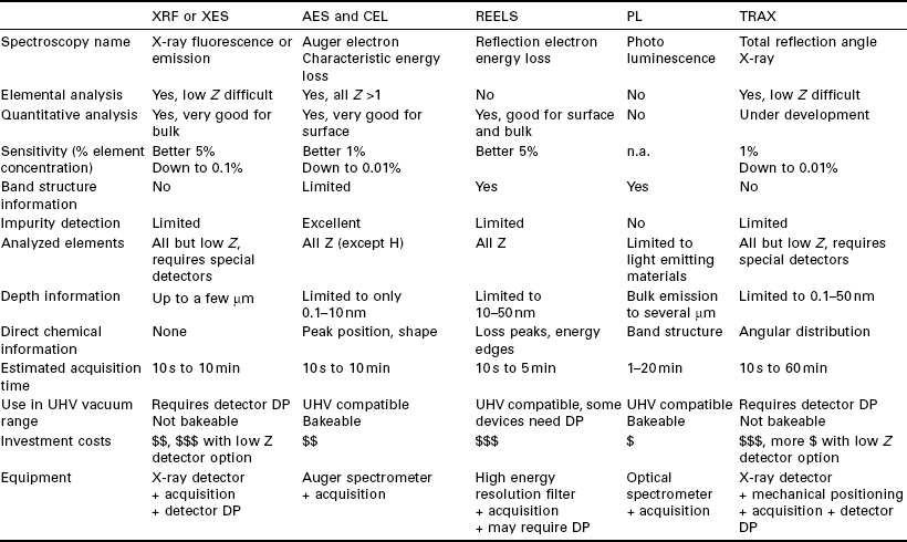
The different aspects of in situ during growth analytical techniques using the RHEED electron beam are summarized in Table 7.1. The main physical parameters are presented as well as a rating of the performance and cost. The figures and values presented in the table should not be taken too literally, but rather as describing the standard capabilities of the technique, thus making an abstraction of exceptional figures that can be reached only under the most favorable experimental conditions.
Table 7.1
Comparison of available in situ, real-time spectroscopies using the RHEED electron beam as excitation. Some values indicated are best estimates based on the author’s available information
For some surfaces, forming known stoichiometric compounds with known atomic concentrations, the calibration of the signals can be performed in situ. For alloy materials, quantitative calibrations are commonly improved by performing a cross-calibration measuring reference samples in other carefully calibrated equipment. The most usual techniques for calibration are RBS, XPS, and secondary ion mass spectroscopy (SIMS). XPS devices are often mounted in a separate vacuum chamber connected to the growth chamber that allows in situ analyses. Normally, only a few samples need to be cross-calibrated in order to build a set of sensitivity factors.
In spite of their strong potential capabilities, it is likely that the use of the above described in situ spectroscopies will be limited to specific applications where the growth must not only be controlled by the material fluxes and sample temperature, but also requires control over parameters such as incorporation rate and stoichiometry, knowledge of the layer and interface composition in multilayered samples, or simply control of impurities eventually co-deposited during the growth. For these challenging cases, the above techniques, especially with regards to their new improvements, should become a welcome addition to the usual growth control techniques described in this book.
7.6 Sources of further information and advice
Drouin D, CASINO V2.42 – Program available for free from: http://www.gel.usherbrooke.ca/casino/What.html.
Jablonski, A., Tougaard, S. NIST Elastic Electron Scattering Cross Sections Database. In: NIST Reference Database 64. US Department of Commerce and Technology; 2010.
Mucal, Fluorescence yields and X-ray energies. Available from: http://www.csrri.iit.edu/mucal.html.
NIST database 64. Electron Elastic Scattering Cross Sections. Available from: http://physics.nist.gov/asd3, 2010, September 6. [National Institute of Standards and Technology, Gaithersburg, MD].
Ralchenko, Y., Kramida, A.E., Reader, J., NIST ASD Team. NIST Atomic Spectra Database (version 3.1.5). Available from: http://physics.nist.gov/asd3, 2010, September 6. [National Institute of Standards and Technology, Gaithersburg, MD].
7.7 References
Briggs, D., Grant, J. Surface Analysis by Auger andX-Ray Photoelectron Spectroscopy. IM Publications and Surface Spectra Limited. 259, 2003.
Calley, L., Staib, P., Lowder, J., Doolittle, A., An Auger electron analyzer system for in situ MBE growth monitoring. Proceeding European MRS TuP33. 2011.
Chambers, S.A., Tran, T.T., Hilman, T.A. Auger electron spectroscopy as a real-time compositional probe in molecular beam epitaxy. J Vac Sci Tech A. 1996; 13(1):83.
Chandril, S., Keenan, C., Myers, T.H., Lederman, D. In situ thin film and multilayer structural characterization using X-ray fluorescence induced by reflection high energy electron diffraction. J Appl Phys. 2009; 106:024308.
Ding, Z.J., Salma, K., Li, H.M., Zhang, Z.M., Tokesi, K., Varga, D., Toth, J., Goto, K., Shimizu, R. Monte Carlo simulation study of electron interaction with solids and surfaces. Surf Interface Analysis. 2006; 38:657.
Disko, M.M., Ahn, C.C., Fultz, B. Transmission Electron Energy Loss Spectrometry in Materials Science. Metals & Materials Society (TMS): The Minerals; 1992.
Drouin, D., Real, A., Couture, D., Joly, X., Tastet, V., Aimez, Gauvin R. CASINO V2.42 – a fast and easy-to-use modeling tool for scanning electron microscopy and microanalysis users. Scanning. 2007; 29:92–101.
Egerton, J. Transmission Electron Energy Loss Spectrometry in Material Science. Metals & Materials Society (TMS): The Minerals; 1992.
Everhart, T.E. Simple theory concerning the reflection of electrons from solids. J Appl Phys. 1960; 31:1483.
Everhart, T.E., Hoff, P.H. Determination of kilovolt electron energy dissipation vs penetration distance in solid materials. J Appl Phys. 1971; 42:5837.
Ferguson, I. Auger Microprobe Analysis. Adam Hilger IOP Publishing. 25, 1989.
Grant, J., Surface Analysis by Auger and X-ray Photoelectron Spectroscopy. Briggs, D., Grant, J., eds. 2003. [IM Publications and Surface Spectra Ltd, Chapter 3].
Gryzinski, M. Two-particle collisions. I. General relations for collisions in the laboratory system. Phys Rev. 138, 1965. [A305, A322, A336].
Hasegawa, S., Ino, S., Yamamoto, Y., Daimon, H. Chemical analysis of surfaces by total-reflection-angle X-ray spectroscopy in RHEED experiments (RHEED-TRAXS). Jpn J Appl Phys. 1985; 24(6):L387.
Hashimoto, M., Arkun, F.E., Jackson, A., Clark, A., Smith, R., Sewell, R., Palmstr0m, C.J., In-situ compositional analysis of rare earth binary and ternary, oxides by energy dispersive X-ray spectroscopy during MBE growth. Proceeding NAMBE 2009. 2009. [VII.2].
Ichimura, S., Shimizu, R. Backscattering correction factor for quantitative analysis. Surf Sci. 1981; 112:386.
Ino, S., Ichikawa, T., Okada, S. Chemical analysis of surface by fluorescent X-ray spectroscopy using RHEED-SSD method. Jpn J Appl Phys. 1980; 19:1451.
Kanter, H. Electron mean free path near 2 keV in aluminum. Phys Rev. 1970; B1:2357.
Krause, M.O. Atomic radiative and radiationless yields for K and L-shells. J Phys Chem, Ref Data. 8, 1979. [307 (1079)].
Leapman, R., EELS quantitative analysis. Disko, M.M., Ahn, C.C., Fultz, B., eds. 1992. [Minerals, Metals & Materials Society, Chapter 3].
Lee, K., Myers, T.H. The use of cathodoluminescence during molecular beam epitaxy growth of gallium nitride to determine substrate temperature. J Electronic Mater. 2007; 36(4):431.
Lightowlers, E.C., Photoluminescence Characterization, Growth and Characterization of Semiconductors. Stradling, R.A., Klipstein, P.C. Adam Hilger Publisher, 1990.
Moretti, G. Surface Analysis by Auger and X-Ray Photoelectron Spectroscopy. IM Publications and Surface Spectra Limited. 501, 2003.
Moulder, J.F., Stickle, W.F., Sobol, P.E., Bomben, K.D. Appendix A. In: Handbook of X-Ray Photoelectron Spectroscopy. Perkin-Elmer Corporation; 1992.
Murata, K. Spatial distribution of backscattered electrons in the scanning electron microscope and electron microprobe. J Appl Phys. 1974; 45:4110.
Nikzad, S., Ahn, C.C., Atwater, J. Quantitative analysis of semiconductor alloy composition during growth by reflection-electron energy loss spectroscopy. J Vac Sci Tech. 1992; B10:762.
Pellegrino, J.G., Armstron, J., Lowney, J., DiCamillo, B., Woicik, J.C. Electron beam induced X-ray emission: an in situ probe for composition determination during molecular beam epitaxy growth. Appl Phys Lett. 1998; 73:3580.
Powell, C. NIST Standard Reference Database 71, ‘Electron Inelastic-Mean-Free-Path: Version 1’. Available from: http://www.nist.gov/data/nist71.htm, 2000.
Raether, H., Excitation of Plasmons and Interband Transitions by Electrons Springer Verlag. Springer Tracts in Modern Physics 1980; 88
Ramaker, D.E. Surface Analysis by Auger and X-Ray Photoelectron Spectroscopy. IM Publications and Surface Spectra Limited. 465, 2003.
Reimer, L. Scanning Electron Microscopy. Springer Verlag; 1985.
Sevier, K.D. Low Energy Electron Spectroscopy. New York: Wiley Interscience; 1972. [356].
Sewell, P.B., Cohen, M. Reflection high energy electron diffraction and X-ray emission analysis of surfaces and their reaction products. Appl Phys Lett. 1967; 11(9):298.
Small, J.A., Leigh, S.D., Newbury, D.E., Myklebust, R.L. Modeling of the bremsstrahlung radiation produced in pure-element targets by 10–40 keV electrons. J Appl Phys. 1987; 61(2):459.
Sogard, M.R. Backscattered electron energy spectra for thin films from an extension of the Everhart theory. J Appl Phys. 1980; 51:4412.
Staib, P. In situ real time Auger analyses during oxides and alloy growth using a new spectrometer design. J Vac Sci Technol B. 29, 2011. [03C125].
Staib, P., Tappe, W., Contour, J.P. Imaging energy analyzer for RHEED: energy filtered diffraction patterns and in situ electron energy loss spectroscopy. J Cryst Growth. 1999; 201(202):45–49.
Strawbridge, B., Shinh, R.K., Beach, C., Mahajan, S., Newman, N. Effect of surface topography on reflection electron energy loss plasmon spectra of group III metals. J Vac Sci Technol A. 2006; 24(5):1776.
Sun, B., Goodrich, T.L., Ziemer, K.S. Using RHEED-TRAXS to understand complex oxide growth mechanisms. Proceeding NAMBE 2009. 2009.
Tanuma, S., Surface Analysis by Auger and X-Ray Photoelectron Spectroscopy. Briggs, D., Grant, J. IM Publications and Surface Spectra Limited, 2003. [259].
Tompkins, R.P., VanMil, B.L., Schires, E.D., Lee, K., Chye, Y., Lederman, D., Myers, T.H. In-situ investigation of surface stoichiometry during InGaN and GaN growth by plasma-assisted molecular beam epitaxy using RHEED-TRAXS. 0892-FF04-06. Mat Res Soc Symp Proc. 2006; 892:1–5.
Wagner, C.D. Auger lines in X-ray photoelectron spectrometry. Anal Chem. 1972; 44(6):967.
Wagner, C.D., Riggs, W.M., Davis, L.E., Moulder, J.F., Mullenberg, G.E., Handbook of X-Ray Photoelectron Spectroscopy. Perkin Elmer Corporation (Physical Electronics). 1st, 1979.
Wang, Z.L. Reflection Electron Microscopy and Spectroscopy for Surface Analysis. Cambridge University Press; 1996.
Werner, S., Surface Analysis by Auger and X-ray Photoelectron Spectroscopy. Briggs, D., Grant, J. IM Publications and Surface Spectra Limited, 2003. [Chapter 10].
Werner, S. Electron Transport in Solids for Quantitative Surface Analysis. Available from http://eaps4.iap.tuwien.ac.at/~werner/Si_pl.dat, 2010.
Williams, G. Electron Energy Level Binding Energies. Available from: www.dovada.com/electron_binding.htm, 2006.
ZAF from NIST. Available from: http://www.cstl.nist.gov/div837/Division/outputs/DTSA/chapters/Analysis.html#DZ Lecture on ZAF, Available from: http://web.pdx.edu/~jiaoj/phy451/Lect8.pdf.