
X-ray photoelectron spectroscopy (XPS) for in situ characterization of thin film growth
Abstract:
X-ray photoelectron spectroscopy (XPS) is an excellent tool for the investigation of the growth and reaction of thin films. Owing to the short mean free path of electrons in condensed matter, XPS is particularly well suited for the measurement of films with thicknesses of up to a few nanometers. XPS allows for the quantitative determining of the elemental composition, chemical specificity (i.e., oxidation state) and film thickness. In this chapter the basics of XPS are described, including different approaches to monitoring in situ film growth and reactions.
4.1 Introduction
X-ray photoelectron spectroscopy (XPS) is one of the most commonly used surface science techniques.1–4 It is based on the photoelectric effect,5 where an X-ray photon is absorbed by a core or valence electron. If the incident photon energy is larger than the binding energy of the electron, the electron will be emitted. The basic set-up of an XPS experiment is shown in Fig. 4.1. Monochromatic X-rays from a laboratory source (X-ray tube) or from a synchrotron irradiate the sample. The emitted electrons are collected by an electrostatic lens and energy-analyzed by a spectrometer, most commonly a hemispherical electron energy analyzer. From the known photon energy hv and the measured kinetic energy KE, the binding energy BE of the electrons can be determined according to BE = hv – KE Φ, with Φ as the spectrometer work function. Typical incident photon energies in an XPS experiment range from several 10s to well over 1000 eV, with kinetic energies of the same order.

4.1 Basic set-up of an XPS experiment. The sample is irradiated by monochromatic X-rays. The kinetic energy of the emitted photoelectrons is analyzed by an electron analyzer. Reprinted with permission from Ertl and Küppers.3 Copyright (1985), Wiley-VCH Verlag GmbH & Co. KGaA.
While the penetration depth of the X-rays into the sample is of the order of hundreds of nanometers or more,6 elastic and inelastic interactions of photoelectrons with atoms in the sample limit the probed depth to a maximum of a few nanometers over the kinetic energy range used in conventional XPS studies. Figure 4.2 shows the inelastic mean free path (IMFP) of electrons as a function of their kinetic energy in Cu; the minimum path length is at about 100 eV kinetic energy (see Fig. 4.2).7 This surface sensitivity makes XPS particularly well suited for the study of ultrathin films with only a few monolayer or less in thickness. Figure 4.2 also shows that the IMFP increases with increasing kinetic energy, e.g., in the case of Cu up to about 10 nm at a kinetic energy of 10 keV. With the use of high-brilliance synchrotrons that provide X-rays in this energy range, the study of thick multilayer system and buried interfaces has become feasible, as will be discussed later in this chapter. It should be noted that the inelastic mean free path is not a precise description of the actual probing depth in an XPS experiment, since it neglects elastic scattering effects. A more accurate quantity for the measurement depth is the effective attenuation length (EAL), which includes elastic scattering effects.8

4.2 Inelastic mean free path as a function of kinetic energy of electrons in copper. The graph shows calculated data from: Tanuma et al., Surf. Interface Anal., 17, 911 (1991); Ashley, J. Electron Spectrosc. Rel. Phenom., 50, 323 (1990); Kwei et al., Surf. Sci., 293, 202 (1993); as well as Ding and Shimizu, Scanning, 18, 92 (1996). Experimentally determined IMPF values from elastic peak electron spectroscopy measurements and Monte Carlo simulations are also shown (Powell and Jablonski, J. Phys. Chem. Ref. Data, 28, 19 (1999)). Reprinted with permission from Powell and Jablonski.8 Copyright (2009), Elsevier BV.
While the short mean free path of electrons in matter makes XPS an exquisitely surface-sensitive method, it also requires in general high vacuum conditions during the measurements, since the emitted photoelectrons are also scattered by gas phase molecules. For example, the mean free path of 100 eV electrons (i.e., those with the highest surface sensitivity) is about 1 mm in 1 torr of water vapor. Since the electrons travel many centimeters on their way to the electron detector, attenuation of the signal under elevated pressure conditions poses a limit on the background pressure in conventional XPS set-ups. Over the years, different schemes for in situ XPS measurements have been developed that now allow measurements at pressures in the torr range, as will be shown later in the chapter.
The advantages of XPS for the investigation of thin films are its surface sensitivity and chemical specificity. Since each element exhibits a characteristic set of core level peaks in XPS, the chemical composition of the surface and near-surface region of a sample can be determined quantitatively. Moreover, the binding energy of core and valence electrons shows subtle changes (of the order of tenths to several eV) depending on the chemical bonding (e.g., the oxidation state). This allows the discrimination, for instance, of Si atoms in an oxide layer (~Si4 +) from Si atoms at the interface (~Si1 +, Si2 +, Si3 +) and elemental Si in the substrate (Si0) of a Si wafer covered by a native oxide layer (see Fig. 4.3).9 When interpreting these so-called ‘chemical shifts’, one has to keep in mind that the binding energy depends both on the state of the atom before the photoemission event (‘initial state effects’) as well as contributions due to the reorganization of the electrons in the atom during the relaxation process, when the core hole is filled (‘final state effects’). It is, however, in many cases possible to assign chemical shifts to initial state effects. For instance, the observed chemical shifts for the different Si species in Fig. 4.3 can be rationalized by different degrees of charge transfer from Si to O (depending on the Si oxidation state), which leads to variations in the screening of the Si 2p electrons by Si 3s and 3p valence electrons. Thus, the 2p electrons in the case of Si4 + experience a stronger Coulomb attraction to the nucleus than in Si3 +, resulting in a higher binding energy in the case of Si4 +. This sensitivity to the chemical state of the atoms means that valuable information can be gleaned from XPS measurements about, e.g., bonding within thin films, at the surface, as well as at the interface to the substrate (see Fig. 4.3).
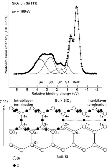
4.3 Upper panel: Si 2p XPS spectrum for SiO2/Si(111). The diamonds are data points, and the curves show a fit and the decomposition into components. Lower panel: model for the SiO2/Si(111) interface. Two possible terminations are shown. The labels indicate the oxidation states for Si atoms at and near the interface. Reprinted with permission from Sieger et al.9 Copyright (1996), by the American Physical Society.
XPS can also be used to determine the thickness of deposited layers on a substrate, assuming ideal layer-by-layer growth and smooth interfaces. For a single layer with homogeneous chemical composition and thickness dm, the detected intensity Im, using the straight-line approximation, is given by2,10
with λm′ = λm cos(α) as the effective attenuation length at angle a between the surface normal and detector position (see Fig. 4.4), λm the attenuation length of electrons for layer m at a given kinetic energy, and z the depth measured from the layer surface. The factor S contains a number of experimental parameters and is given for layer m and inner shell orbital j by:

4.4 Model for a multilayer system consisting of n homogeneous layers above a bulk substrate, where the order of stacking from bottom to top is given by layer 1, layer 2, …, layer n. The detection angle of the electron analyzer with respect to the surface normal is α. The effective probing depth λ′ is given by the electron attenuation length λ times cos(α).
with Φ as the X-ray flux at a given X-ray energy (hv), σ the photoemission cross-section11 at a given hv, β the orbital specific asymmetry parameter, D the spectrometer efficiency for a given kinetic energy, and N the number of atoms per unit volume. For an infinitely thick layer with dm → ∞ (i.e., a bulk substrate), the intensity is Isubs = Ssubsjλsubs′.
For a multilayer system consisting of n homogeneous layers above a bulk substrate (see Fig. 4.4), where the order of stacking from bottom to top is given by layer 1, layer 2, …, layer n, the XPS intensity from the substrate is attenuated by each layer according to the Beer– Lambert law:12
Likewise, the intensity of layer m in a system of n layers is being attenuated by (n – m) layers, and is thus given by:
There are two principal methods to obtain depth-dependent elemental and chemical information using XPS: (1) depth-profiling by etching (for instance with argon ions), where surface layers are gradually removed by sputtering, while XPS spectra are obtained at various stages during the removal of surface layers, and (2) non-destructive depth profiling through the variation of the escape-depth of the electrons, either by varying the detection angle relative to the sample surface or by measuring photoelectrons with different kinetic energies. The advantage of depth profiling by argon etching is that it is not limited by the escape depth of the electrons, so that information about the sample from depths in excess of several nm can be obtained. The disadvantage is that the sample surface is destroyed in the process, and that the chemical state of the surface may be altered due to the impact of Ar ions.13
Non-destructive depth profiling in an XPS experiment that uses an X-ray source with a fixed energy (i.e., a lab-based experiment) relies on the variation of the take-off angle α of the photoelectrons (see Fig. 4.4), which determines (at a fixed kinetic energy) the information depth in the experiment.2,14 An example for this technique is shown in Fig. 4.5 for the case of a 4 nm thick SiOxNy film on a Si substrate.15 The relative intensity of the Si4+ peak is clearly enhanced at shallow detection angle. The schematic representation of the electron trajectories in Fig. 4.5 also illustrates that the depth resolution in angle-resolved XPS depends on the angular acceptance of the electrostatic analyzer, which should be ideally as narrow as possible. Since the effective probing depth λ′ varies with the take-off angle α according to λcos(α) (with λ as attenuation length), the most sensitive determination of the film thickness is at the most grazing detection angles. Measurements at these angles, however, are hampered by surface roughness effects, which need to be taken into account.14

4.5 (a) Schematic depiction of an angle-resolved XPS experiment for the measurement of the chemical states and composition of SiOXNY films on a Si substrate. (b) Si 2p XPS spectra of a 4 nm SiOXNY film, taken at 15° and 75° take-off angles. The relative intensity of Si0 to Si4 + is enhanced with increasing take-off angle (TOA). Reprinted with permission from Chang et al.15 Copyright (2000), American Institute of Physics.
The use of variable incident photon energies (and thus kinetic energies) for depth profiling is performed using a fixed sample–detector geometry and is thus not influenced by surface geometry effects. This method requires a photon source with variable energy, such as a synchrotron. The technique makes use of the dependence of the mean free path of electrons in matter on their kinetic energy (see Fig. 4.2). An example is shown in Fig. 4.6, where the growth of praseodymium-SiO2 layers on Si was monitored using XPS.16 Figure 4.6(a) shows Si 2p spectra after each preparation step: first after the growth of a 2.6 nm thick SiO2/Si film, then after the deposition of 1 nm of metallic Pr on top of SiO2, and finally after annealing the sample to 600 °C, which leads to incorporation of Pr into SiO2 in a solid state reaction. under each condition Si 2p spectra were taken with kinetic energies of 440, 660 and 920 eV, with the most surface-sensitive spectrum at 440 eV and the most bulk sensitive at 920 eV. The spectra after annealing show a strong peak at a binding energy of ~102 eV in addition to the Si0 and Si4 + peaks due to the substrate and the SiO2 film, respectively. The peak at 102 eV is attributed to the formation of Pr silicate, which is located predominantly at the sample surface, as the depth profiling spectra after post-deposition annealing (or PDA, in Fig. 4.6a) prove. This scenario is confirmed by cross-sectional transmission electron microscopy images that were taken after the reaction (Fig. 4.6b).
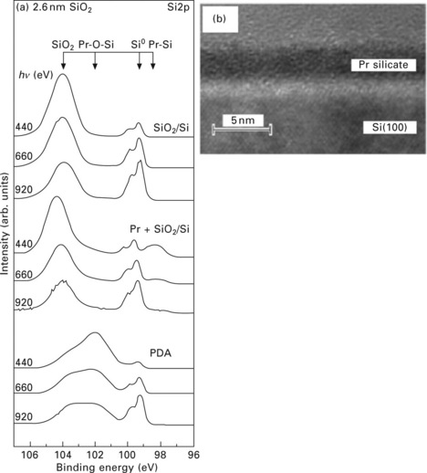
4.6 (a) Si 2p spectra taken at different photoelectron kinetic energies during the preparation of Pr-SiO2 layers on a Si substrate. (b) Transmission electron microscopy cross-sectional images of the film shown in (a). Reprinted with permission from Lupina et al.16 Copyright (2005), American Institute of Physics.
To summarize so far, XPS is a quantitative method for the determination of thin film elemental composition and chemistry and can also be used under favorable circumstances to determine the film thickness, as well as to distinguish surface from bulk species. The following section discusses how XPS can be used to in situ monitor thin film growth, the reaction of thin film surfaces with adsorbates and gases, as well as the chemistry of solid/solid interfaces in multilayer systems. Some of these investigations required the development of new XPS instrumentation, which will be discussed alongside the experimental results.
4.2 In situ monitoring of thin film growth
Studying the elemental and chemical composition as well as the thickness of thin films in situ during film growth using XPS requires an expansion of the technique to pressures in the mtorr range. The first dedicated XPS instrument for monitoring thin film growth was described by Kelly et al. in 2001.17 A schematic of the instrument is shown in Fig. 4.7. This system is capable of operating at pressures in the 10−3 torr range, about three orders of magnitude higher than the pressure limit in conventional XPS systems. The X-ray source (Mg Kα anode) is separated from the gas atmosphere in the measurement chamber by a 2 μm thick aluminum foil, which is about 70% transparent for Mg Kα radiation (1254 eV).6 The electrostatic lens system of a commercial hemispherical analyzer was modified by introducing a 1 mm diameter differentially pumped aperture in the lens column. Two spherical stainless steel meshes are mounted in front of the standard input lens to collect and focus electrons from the sample onto the differentially pumped aperture (see Fig. 4.8). After passing through the meshes the electrons are accelerated to energies between 1000 to 1300 eV, which decreases the lens magnification to about 1 and also decreases the scattering of electrons by gas molecules due to the high electron kinetic energy. At the given lens magnification the electron analyzer measures a sample area of about 1 mm diameter.

4.7 Set-up of an XPS spectrometer for the in situ monitoring of thin film layer deposition. A conventional Mg Kα X-ray source is separated from the elevated pressure in the experimental chamber by a 2 μm thick Al foil. The differentially pumped electron lens focuses emitted photoelectrons through a small aperture with a two orders-of-magnitude pressure differential across it. The electrons are then imaged onto the spectrometer entrance slit into a still lower pressure region. Reprinted with permission from Kelly et al.17 Copyright (2001), American Vacuum Society.
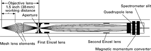
4.8 Detailed schematic view of the electrostatic lens system used in the spectrometer shown in Fig. 4.7. Reprinted with permission from Kelly et al.17 Copyright (2001), American Vacuum Society.
The pressure differential between the measurement/thin film growth chamber and the hemispherical analyzer was 3–4 orders of magnitude, providing the necessary pressure difference for operation at mtorr pressures in the experimental chamber. Other considerations in the design of the spectrometer included high-speed acquisition of spectra to follow film growth with high-time resolution, a large working distance (~3 to 5 cm) between the electrostatic analyzer input lens and the sample to avoid interference by the electrostatic lens system with the reactant flow to the sample, as well as the suppression of stray electrons and ions that may be generated in plasmas near the growing surface.17 The latter is achieved by biasing the meshes in the input lens positively at 20 V (thus rejecting slow ions) and operating the lens elements in a manner that reduces the transmission of secondary electrons. High data acquisition speed was achieved by a large collection angle of the electrostatic lens (30° total) and the use of an imaging electron detector that measures a range of electron energies simultaneously.
A case study for the application of this instrument is shown in Fig. 4.9. The growth of a thin film of tungsten oxide on a Si substrate was monitored by measuring the W 4f, O 1s and Si 2p core level peaks (see upper panel in Fig. 4.9). The acquisition time for each spectrum is 30 s. The initial substrate surface shows the characteristic Si 2p peaks for a native oxide layer on a Si substrate, where the peak in the O 1s spectrum is purely due to the native silicon oxide layer. Tungsten is evaporated onto the substrate from a hot filament in a background of 1 mtorr of oxygen. The evolution of the W 4f, O 1s and Si 2p peaks during deposition shows a decrease in both the Si and SiOX peaks due to attenuation of Si photoelectrons by the deposited layer. As expected, the W 4f signal increases with increasing deposition time. The same holds for the O 1s intensity, which indicates that oxygen is incorporated into the growing film, since the initial oxygen intensity was only due to oxygen in SiO2, and the Si 2p peak of SiO2 decreases with time. The integrated intensities for Si 2p, O 1s and W 4f as a function of deposition time are plotted in the bottom panel of Fig. 4.9.

4.9 (a) W 4f, O 1s and Si 2p spectra obtained in situ during the growth of a WOX film on a SiO2/Si substrate using the spectrometer shown in Fig. 4.7. (b) Integrated XPS peak intensities plotted as a function of time. Reprinted with permission from Kelly et al.17 Copyright (2001), American Vacuum Society.
The Si 2p and W 4f spectra at deposition times of ~11 min (‘A’) and ~61 min (‘B’) are displayed in Fig. 4.10, upper panels.17 The Si 2p spectra show a decrease in intensity in both the SiO2 and the elemental Si 2p peaks, as expected for the growth of a layer at the surface. The W 4f spectra initially show the characteristic binding energy for a WO3 species (‘A’), while at later deposition times some elemental W is also observed. By relating the Si 2p intensity of the pristine substrate to the Si 2p intensity at various stages during deposition, the attenuation of the Si 2p signal can be used to determine the thickness of the WOx film (see Eq. [4.3]). With the detection angle at 25° from the sample normal, and assuming an attenuation length of 1.8 nm for the Si 2p electrons (kinetic energy ~1150 eV), the escape depth of the electrons in the experiment is 1.8 nm × cos(25°) ~1.6 nm. Using these values, a model for the thickness of the SiO2 and WOX layers at different stages during the deposition can be postulated (bottom panel of Fig. 4.10).
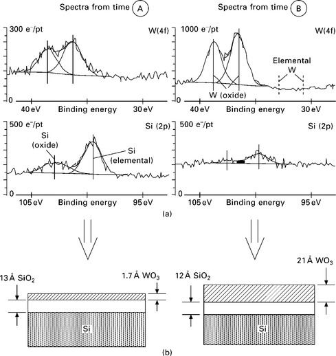
4.10 (a) Detailed Si 2p and W 4f spectra taken after 11 (A) and 61 minutes (B) during the growth of a WOX film on SiO2/Si substrate (e−/pt = number of electrons per unit (point) on /-axis). (b) A model for the evolution of the WOx film with time can be postulated from the integrated peak intensities as well as the probing depth in the experiment. Reprinted with permission from Kelly et al.17 Copyright (2001), American Vacuum Society.
Apart from the experiments shown in Figs 4.9 and 4.10, this instrument has also been used to monitor the deposition of Al2O3 on InGaAs,18,19 and the oxidation of Ge(100).20 While the performance of the current set-up used in the case studies described above provided hitherto unavailable opportunities for in situ film growth monitoring, Kelly et al. estimated that the performance of the instrument can be increased by more than an order of magnitude through two measures: (a) increasing the acceptance angle of the spectrometer to 40°, and (b) by use of a state-of-the-art focused X-ray source instead of the unfocused one which is used in the current set-up. A focused X-ray source would increase the X-ray flux in the 1 mm2 field of view of the detector by more than a factor of 10. This would then allow the acquisition of the order of one spectrum per second, an improvement of a factor > 10 over the current speed. If in addition the lens design were modified so that the acceptance area of the lens is increased to 4 mm2, another factor of 10 in acquisition speed could be gained, making it possible to collect 10 spectra per second. Even though these improvements are challenging, they are merely technical in nature; monitoring film growth with a time resolution of 0.1 s should therefore be possible in the future.
4.3 Measuring the reaction of thin films with gases using ambient pressure X-ray photoelectron spectroscopy (XPS)
In the following we will focus on the reaction of gases with thin films. Ultrathin oxide, metal, organic as well as semiconductor films play an ever-increasing role in technological applications, including industrial catalysis and data storage devices. The interaction of these systems with reactants as well as environmental gases (such as water vapor) has great influence on their performance and longevity. In particular in the field of heterogeneous catalysis the correlation between the yield and conversion in a catalytic reaction (measured by the composition of the gas phase) with the chemical nature of the active catalyst surface is of great importance for a better understanding of the basic, atomic scale processes in a catalytic reaction, and may lead to a rational design of more efficient catalytic materials.
On the other hand, thin film systems can also be used to study surface reactions, in particular phase transitions and volatilization processes21 that are difficult to quantify in a bulk system. This is illustrated in Fig. 4.11. The upper panel shows the scenario for a bulk sample that interacts with the gas environment and forms a reacted layer at its surface. Photoelectrons with a certain escape depth (symbolized by the length of the arrow) are used to monitor the reaction. If the reaction also involves volatilization, this process is not detectable in an experiment on a bulk sample: the sample on the left will give an identical signal in an XPS experiment as the sample on the right in the upper panel. However, if one uses a thin film sample instead (lower panel, Fig. 4.11) where the film thickness is of the order of the escape depth of the electrons, the attenuation of the substrate electrons can be used to gauge the degree of volatilization of the film, or of its partial conversion into another phase. In addition, since the sample under investigation has a finite thickness of the order of the escape depth of the electrons, the signal of the sample itself can be used to measure the volatilization or conversion of the material into another phase. In essence, thin film samples are, under certain circumstances, superior to bulk samples to monitor gas/surface interactions. It is, however, necessary to point out two caveats. It has been shown that thin film systems can show markedly different properties from their bulk counterparts; this is in part their appeal for the tuning of reaction properties in catalysis.22 In addition, all the above considerations hold only true in the absence of morphological changes (i.e. deviations from a strictly two-dimensional model) to the film and substrate–film interface; such changes would make the quantitative analysis of thickness changes challenging.

4.11 Volatilization and phase transition reactions are easier to quantify in a thin film system than for a bulk sample. For details see text.
The investigation of the reaction of surfaces with gas phase species needs to bridge the so-called ‘pressure gap’ in surfaces science. In the case of XPS this is hampered by the strong interaction of electrons with gas phase molecules, as pointed out in the section above. The differentially pumped electrostatic lens designed by Kelly et al. afforded measurements at pressures in the mtorr range.17 Many reactions, in particular in environmental science, require higher pressures: in order to measure, e.g., the surface of neat liquid water the water vapor pressure in the experimental chamber has to be at least 4.6 torr, which is the equilibrium water vapor pressure at the triple point.
To achieve higher pressures in an XPS experiment, the path length of the electrons through the high-pressure region has to be kept as short as possible. In addition, several differential apertures are necessary to keep the electron analyzer in a high-vacuum environment. This basic concept (see Fig. 4.12a and b) was developed more than 30 years ago in the original designs by Hans & Kai Siegbahn and collaborators, which allowed experiments of up to 1 torr.23,24 Several other groups built instruments based on this concept.25–27 To overcome the trade-off between an increase in detection efficiency through larger apertures on one hand, and better differential pumping through smaller apertures on the other hand, the latest generation of these instruments uses electrostatic lenses that are placed between the apertures, raising the pressure limit to more than 5 torr.28–31 The increase in the pressure limit is also partly due to the use of synchrotron radiation, which offers higher photon flux and tighter focused X-ray beams. Since the instruments operate at realistic environmental humidities, the technique is often called ambient pressure XPS (APXPS). Review articles on the basics and applications of APXPS can be found in Refs. 29, 32, 33 and 34.

4.12 Principle of APXPS instruments. (a) The sample is mounted in a high-pressure chamber, close to a differentially pumped aperture through which electrons and gas escape. The X-ray source is separated from the high-pressure cell by an X-ray-transparent window. (b) To maintain a vacuum better than 10−6 torr for typical entrance aperture diameters of ~1 mm and pressures in the torr range in the sample cell, several differential pumping stages are needed. There is a trade-off between the pumping efficiency, which increases with aperture spacing and decreasing aperture sizes, and the collection efficiency of electrons, which is determined by the solid angle that is subtended by the apertures. (c) In a differentially pumped electrostatic lens system the electrons are focused onto the apertures between the differential pumping stages, thus increasing the transmission of electrons through the differential pump stages and allowing for reduced aperture sizes for improved differential pumping. Reprinted from Bluhm.34 Copyright (2010), with permission from Elsevier.
The application of APXPS to the study of the reaction of thin films is now illustrated using the example of the interaction of a 4 monolayer (ML) thick MgO(100) film grown on a Ag(100) substrate with water vapor. Due to its simple rock salt structure, MgO(100) is an ideal model metal oxide surface for studying the metal oxide–water interface, both theoretically and experimentally.35 Of special interest is the nature of the interaction of water vapor with MgO, in particular molecular vs dissociative adsorption. In this case study, MgO(100) was grown on Ag(100) by vapor deposition following the method reported by Wollschläger et al.36 Magnesium was deposited at a rate of ~0.1 nm min−1 in the presence of 10−6 torr O2 while maintaining the Ag(100) substrate at 300 °C. The interaction of water with the MgO(100) film surface was then studied by monitoring the O 1s and Ag 3d spectra in isobar experiments, where the water vapor pressure was kept constant while the sample temperature was decreased from well over 300 °C to below room temperature.37 Figure 4.13 shows O 1s, Ag 3d, as well as C 1s spectra taken in a 0.15 torr isobar experiment. The O 1s spectrum exhibits four peaks assigned to (from low to high binding energy) oxide, hydroxide, adsorbed molecular water, and water vapor (the gas phase in front of the sample is also partly detected in the experiment). A comparison of the O 1s spectrum at a relative humidity of 0.008% with the one at 6% shows major changes in the MgO film: there is a strong increase of hydroxide uptake as well as water adsorption at higher humidity. The Ag 3d spectra do not show any change (apart from attenuation), which indicates that the MgO film is covering the whole of the Ag(100) substrate, thus preventing a reaction between water vapor and Ag substrate. In addition, C 1s spectra do show a slight increase in carbonaceous species, which is expected under ambient measurement conditions.34
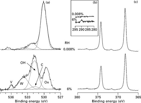
4.13 Ambient pressure XPS O 1s (a), C 1s (b) and Ag 3d (c) spectra taken at a relative humidity of 0.008% and 6% on a 4 ML thick MgO(100)/Ag(100) film. All spectra are taken at an electron kinetic energy of 220 eV. Peak designations in the O 1s spectrum are the metal oxide (Ox), hydroxyl (OH), surface molecular water (W), water vapor (V), and OH contribution due to oxidized carbon species (C). Reprinted from Newberg et al.37 Copyright (2011), with permission from Elsevier.
The O 1s oxide, hydroxide and adsorbed water peak intensity can be converted into equivalent monolayer coverages using a procedure (see Newberg et al. 37) that analyzes both the decrease in Ag 3d signal due to the adsorption of OH and H2O, as well as the relative O 1s signals from the film. The results are plotted in Fig. 4.14. There is a sharp onset of surface hydroxylation at a relative humidity of ~0.01%, accompanied by a reduction in oxide coverage. Water adsorption increases notably at this relative humidity, too. A detailed analysis of the data leads to a model for the reaction of water vapor with MgO(100) under ambient relative humidity, depicted in Fig. 4.15. At a critical relative humidity (~0.01%), water molecules dissociate on the MgO(100) surface, leading to the hydroxylation of the oxygen atoms in the topmost MgO layer, and to the addition of a monolayer of OH groups to the surface. The validity of this reaction mechanism is borne out in the reduction of the total MgO(100) film thickness and the increase in the total O 1s surface signal. This underscores the utility of the application of thin films for the study of surface reactions, as depicted in Fig. 4.11.
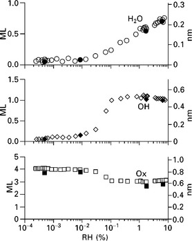
4.14 Integrated O 1s peak intensities from ambient pressure XPS 0.15 torr isobar measurements on 4 ML MgO(100)/Ag(100). Peak assignations are as in Fig. 4.13. The film thicknesses are plotted in units of monolayers (left axis) and nanometers (right axis). 1 ML of Ox, OH, and water are defined as 0.21, 0.48 and 0.31 nm, respectively. Reprinted from Newberg et al.37 Copyright (2011), with permission from Elsevier.
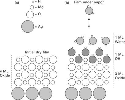
4.15 Illustration of the reaction of a MgO(100)/Ag(100) film with water vapor. (a) Without and (b) with water vapor. In the presence of water vapor at a relative humidity larger than 0.01%, water molecules at the surface dissociate to form two hydroxyl ion moieties: those sitting above the initial MgO interface near Mg2 + surface sites, and those that convert the top layer of MgO oxygen ions to OH−ions. Assuming the entire MgO interface is passivated with OH, the net effect reduces the MgO film from 4 to 3 ML. Reprinted from Newberg et al.37 Copyright (2011), with permission from Elsevier.
4.4 In situ measurements of buried interfaces using high kinetic energy XPS (HAXPES)
In the final part of this chapter we would like to illuminate another promising XPS technique for the in situ study of thin film properties, namely high kinetic energy XPS. This technique has been pioneered by Lindau et al. who demonstrated in 1974 the use of high-energy photons to measure the intrinsic line width of Au 4f core.38 The attraction of high kinetic energy XPS lies in the ability to measure buried interfaces at much larger depths than in conventional soft X-ray XPS (close to 10 nm at 10 keV in the case of Cu, as opposed to close to 1 nm at 1 keV – see Fig. 4.2). However, the detrimental aspects of this technique are the low photoemission cross-sections at high kinetic energies (several orders of magnitude lower than at low kinetic energies) as well as the need for high voltages on the lens elements for sufficient deceleration of electrons for high energy resolution measurements. With the recent availability of high-brightness synchrotron sources the low cross-sections can be compensated for. Figure 4.16 shows recent results for buried SiO2 layers on a Si substrate, which are covered by a NiGe overlayer. Using incident photons with an energy of 7935 eV the authors recorded Si 1s spectra (binding energy ~1840 eV) with electron kinetic energies of over 6000 eV, which allowed probing at a depth of more than 15 nm.39 In another case study the smoothness of the solid/solid interface of buried Ni/Cu interfaces was probed using high kinetic energy XPS.40 Figure 4.17 (upper panel) shows the layout of the sample. Alternate layers of nickel and copper (5 ML each) were deposited on a MgO(100) substrate that was covered by intermediate layers of Fe, Pt, Cu and Ni. This structure was covered by a 1 nm thick Pt cap layer. High kinetic energy (~1200 eV) XPS spectra with a resolution of ~0.25 eV were taken of the Cu 2p core level (bottom panel of Fig. 4.17). Upon heating of the sample from room temperature to 300 °C a marked shift in the Cu 3p3/2 peak position to lower binding energy was observed, which was interpreted as a signature for the smoothing of the Cu/Ni interface.41 These results demonstrate that XPS is not only a valuable tool for the study of the sample surface or near-surface region, but also for investigation of solid/solid interfaces up to a depth of several nanometers.
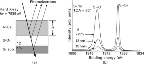
4.16 (a) Experimental parameters of the sample under investigation. (b) Si 1s XPS spectra of the sample shown in (a). The incident photon energy is 7935 eV. Spectral signatures from the SiOX film and the Si substrate can be observed even at a NiGe overlayer thickness of 15 nm. Reprinted from Kobayashi.39 Copyright (2009), with permission from Elsevier.
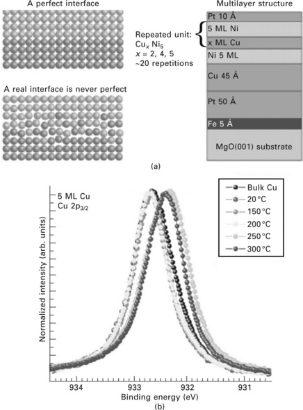
4.17 (a) Left: schematic view of an idealized (top) Ni/Cu interface, where the interfacial roughness is negligible, as compared to a realistic interface (bottom). The right panel shows the configuration of the sample under investigation. (b) Cu 2p3/2 spectra, taken at an incident photon energy of 2010 eV. The shift in the core level binding energy at temperatures above 250 °C indicates a change in the roughness of the Ni/Cu interface. Reprinted from Gorgoi et al.40 Copyright (2009), with permission from Elsevier.
4.5 Conclusions
In summary, X-ray photoelectron spectroscopy is an excellent tool for the investigation of in situ film growth, reaction, as well as the study of buried interfaces. Recent developments of in situ XPS spectrometers as well as high-brilliance synchrotron facilities have expanded the application of XPS to higher pressures as well as larger sampling depths. The challenge for the future lies in the adaption of XPS instruments to realistic environments of thin film growth as well as gas/solid interactions.
4.6 Acknowledgments
The contributions in particular of D. E. Starr, J. T. Newberg, E. R. Mysak, and K. R. Wilson are gratefully acknowledged. This research, the ALS, and the ALS-MES beamline 11.0.2 are supported by the Director, Office of Science, Office of Basic Energy Sciences, Division of Chemical Sciences, Geosciences of the US Department of Energy at the Lawrence Berkeley National Laboratory under Contract No. DE-AC02-05CH11231.
4.7 References
1. Hüfner, S. Photoelectron Spectroscopy, 3rd Ed. Berlin: Springer Verlag; 2003.
2. Briggs, D., Seah, M.P. Practical Surface Analysis, Volume 1 – Auger and X-ray photoelectron spectroscopy, 2nd Ed. Chichester: John Wiley & Sons; 1996.
3. Ertl, G., Küppers, J. Low Energy Electrons and Surface Chemistry, 2nd Ed. Weinheim: VCH Verlagsgesellschaft mbH; 1985.
4. Niemantsverdriet, J.W. Spectroscopy in Catalysis, 2nd Ed. Weinheim: Wiley VCH; 2000.
5. Einstein, A. Über einen die Erzeugung und Verwandlung des Lichtes betreffenden heuristischen Gesichtspunkt. Ann. Physik. 1905; 17:132.
6. 6 Center for X-ray Optics at Lawrence Berkeley National Laboratory (Berkeley, CA); http://henke.lbl.gov/optical_constants/.
7. Seah, M.P., Dench, W.A. Quantitative electron spectroscopy of surfaces: a standard data base for electron inelastic mean free paths in solids. Surface Interface Anal. 1979; 1:2.
8. Powell, C.J., Jablonski, A. Surface sensitivity of X-ray photoelectron spectroscopy. Nucl. Instr. Meth. A. 2009; 610:54.
9. Sieger, M.T., Luh, D.A., Miller, T., Chiang, T.-C. Photoemission extended fine structure study of the SiO2/Si(111) interface. Phys. Rev. Lett. 1996; 77:2758.
10. Fadley, C.S. Angle-resolved X-ray photoelectron spectroscopy. Prog. Surf. Sci. 1984; 16:275.
11. Yeh, J.J., Lindau, I. Atomic subshell photoionization cross sections and asymmetry parameters: 1 < Z < 103. At. Data Nucl. Data Tables. 1985; 32:1.
12. Paynter, R.W. An ARXPS primer. J. Electron. Spectrosc. Relat. Phenom. 2009; 169:1.
13. Briggs, D. Surface Analysis of Polymers by XPS and Static SIMS. Cambridge: Cambridge University Press; 1998.
14. Baird, R.J., Fadley, C.S. X-ray photoelectron angular distributions with dispersion-compensating X-ray and electron optics. J. Electron. Spectrosc. Relat. Phenom. 1977; 11:39.
15. Chang, J.P., Green, M.L., Donnelly, V.M., Opila, R.L., Eng, J., Jr., Sapjeta, J., Silverman, P.J., Weir, B., Lu, H.C., Gustafsson, T., Garfunkel, E. Profiling nitrogen in ultrathin silicon oxynitrides with angle-resolved X-ray photoelectron spectroscopy. J. Appl. Phys. 2000; 87:4449.
16. Lupina, G., Schroeder, T., Dabrowski, J., Wenger, Ch., Mane, A., Lippert, G., Müssig, H.-J., Hoffmann, P., Schmeisser, D. Praesodymium silicate layers with atomically abrupt interface on Si(100). Appl. Phys. Lett. 2005; 87:092091.
17. Kelly, M.A., Shek, M.L., Pianetta, P., Gür, T.M., Beasley, M.R. In situ X-ray photoelectron spectroscopy for thin film synthesis monitoring. J. Vac. Sci. Technol. A. 2001; 19:2127.
18. Shin, B., Clemens, J.B., Kelly, M.A., Kummel, A.C., McIntyre, P.C. Arsenic decapping and half cycle reactions during atomic layer deposition of Al2O3 on In0 53Ga0 47As(001). Appl. Phys. Lett. 2010; 96:252907.
19. Kim, E.J., Chagarov, E., Cagnon, J., Yuan, Y., Kummel, A.C., Asbeck, P.M., Stemmer, S., Saraswat, K.C., McIntyre, P.C. Atomically abrupt and unpinned Al2O3/In0.53Ga0.47As interfaces: experiment and simulation. J. Appl. Phys. 2009; 106:124508.
20. Swaminathan, S., Oshima, Y., Kelly, M.A., McIntyre, P.C. Oxidant prepulsing of Ge(100) prior to atomic layer deposition of Al2O3: in situ surface characterization. Appl. Phys. Lett. 2009; 95:032907.
21. Mysak, E.R., Smith, J.D. J.T, Newberg, P.A. Ashby, K.R. Wilson, H. Bluhm, Competitive reaction pathways for functionalization and volatilization in the heterogeneous oxidation of coronene thin films by hydroxyl radicals and ozone. Phys. Chem. Chem. Phys. 2011; 13:7554.
22. Grönbeck, H. Mechanism for NO2 charging on metal supported MgO. J. Phys. Chem. B. 2006; 110:11977.
23. Siegbahn, H., Siegbahn, K. ESCA applied to liquids. J. Electron Spectrosc. Relat. Phenom. 1973; 2:319.
24. Fellner-Feldegg, H., Siegbahn, H., Asplund, L., Kelfve, P., Siegbahn, K. ESCA applied to liquids IV. A wire system for ESCA measurements on liquids. J. Electron Spectrosc. Relat. Phenom. 1975; 7:421.
25. Joyner, R.W., Roberts, M.W., Yates, K. A ‘high-pressure’ electron spectrometer for surface studies. Surf Sci. 1979; 87:501.
26. Ruppender, H.J., Grunze, M., Kong, C.W., Wilmers, M. In situ X-ray photoelectron spectroscopy of surfaces at pressures up to 1 mbar. Surf. Interf. Anal. 15(245), 1990.
27. Pantförder, J., Pöllmann, S., Zhu, J.F., Borgmann, D., Denecke, R., Steinrück, H.-P. A new set-up for in-situ XP spectroscopy from UHV to 1 mbar. Rev. Sci. Instrum. 2005; 76:014102.
28. Ogletree, D.F., Bluhm, H., Lebedev, G., Fadley, C.S., Hussain, Z., Salmeron, M. A differentially pumped electrostatic lens system for photoemission studies in the millibar range. Rev. Sci. Instrum. 2002; 73:3872.
29. Knop-Gericke, A., Kleimenov, E., Hävecker, M., Blume, R., Teschner, D., Zafeiratos, S., Schlögl, R., Bukhtiyarov, V.I., Kaichev, V.V., Prosvirin, I.V., Nizovskii, A.I., Bluhm, H., Barinov, A., Dudin, P., Kiskinova, M. High-pressure X-ray photoelectron spectroscopy: a tool to investigate heterogeneous catalytic processes. In: Gates, B.C., Knözinger, H., eds. Advances in Catalysis, Vol. 52. Burlington: Academic Press; 2009:213–272.
30. Grass, M.E., Karlsson, P.G., Aksoy, F., Lundqvist, B.W.M., Mun, B.S., Hussain, Z., Liu, Z. New Ambient Pressure Photoemission Endstation at ALS Beamline 9.3.2. Rev. Sci. Instrum. 2010; 81:053106.
31. Ogletree, D.F., Bluhm, H., Hebenstreit, E.L.D., Salmeron, M. Photoelectron spectroscopy under ambient pressure and temperature conditions. Nuclear Instr. Methods A. 2009; 601:151.
32. Salmeron, M., Schlögl, R. Ambient pressure photoelectron spectroscopy: a new tool for surface science and nanotechnology. Surf. Sci. Rep. 2008; 63:169.
33. Bluhm, H., Hävecker, M., Knop-Gericke, A., Kiskinova, M., Schlögl, R., Salmeron, M. In situ photoemission studies of gas/solid interfaces at near atmospheric pressures. MRS Bull. 2007; 32:1022.
34. Bluhm, H. Photoemission spectroscopy under humid conditions. J. Electron Spectrosc. Relat. Phenom. 2010; 177:71.
35. Henrich, V.E., Cox, P.A. The Surface Science of Metal Oxides. Cambridge: Cambridge University Press; 1994.
36. Wollschläger, J., Viernow, J., Tegenkamp, C., Erdos, D., Schroder, K.M., Pfnur, H. Stoichiometry and morphology of MgO films grown reactively on Ag(100). Appl. Surf. Sci. 1999; 142:129.
37. Newberg, J.T., Starr, D.E., Porsgaard, S., Yamamoto, S., Kaya, S., Mysak, E.R., Kendelewicz, T., Salmeron, M., Brown, G.E., Jr., Nilsson, A., Bluhm, H. Formation of hydroxyl and water layers on MgO films studied with ambient pressure XPS. Surf. Sci. 2011; 605:89.
38. Lindau, I., Pianetta, P., Doniach, S., Spicer, W. X-ray photoemission spectroscopy. Nature. 1974; 250:214.
39. Kobayashi, K. Hard X-ray photoemission spectroscopy. Nuclear Instr. Methods A. 2009; 601:32.
40. Gorgoi, M., Svensson, S., Schäfers, F., Öhrwall, G., Mertin, M., Bressler, P., Karis, O., Siegbahn, H., Sandell, A., Rensmo, H., Doherty, W., Jung, C., Braun, W., Eberhardt, W. The high kinetic energy photoelectron spectroscopy facility at BESSY: progress and first results. Nuclear Instr Methods A. 2009; 601:48.
41. Abrikosov, I.A., Olovsson, W., Johansson, B. Valence-band hybridization and core level shifts in random Ag-Pd alloys. Phys. Rev. Lett. 2001; 87:176403.