
Ultraviolet photoemission spectroscopy (UPS) for in situ characterization of thin film growth
Abstract:
This chapter discusses the application of ultraviolet photoemission spectroscopy (UPS) and angle-resolved photoemission spectroscopy (ARPES) to study the electronic structure of thin films synthesized in situ using film growth techniques such as molecular beam epitaxy (MBE) and pulsed laser deposition (PLD). The chapter first describes the principles of photoemission spectroscopy and the current experimental state of this technique. Then, particular examples such as UPS and ARPES studies of in situ thin films of SrRuO3 and La1 − xSrxMnO3 are detailed.
3.1 Introduction
One of the prime motivators for the growth of materials in thin film form is the potential for manipulating their electronic and magnetic properties. One of the forefronts of modern condensed matter physics is the search for new states of quantum matter with exotic physical properties, and thin films and superlattices present a unique opportunity for designing and realizing such novel materials. One way of achieving this control is to create atomically perfect interfaces between two different materials. Modern technologies such as the transistor or laser are dependent on interfacial phenomena. Remarkable scientific discoveries such as the integer and fractional quantum Hall effects (Nobel Prizes 1985, 1998) were discovered at semiconductor interfaces engineered using molecular beam epitaxy (MBE). Since 2005, interfacial phenomena at the atomically abrupt interface between dissimilar materials have yielded a flurry of breakthroughs. To fully benefit from the tailoring of these novel thin film interfaces and heterostructures, one needs to be able to characterize the state of electronic matter created in each system. In order to do so, it will be desirable to utilize sophisticated 21st century tools to achieve this aim, such as high-resolution angle-resolved photoemission spectroscopy (ARPES). The ARPES technique follows from the development of electron spectroscopy for chemical analysis (ESCA) pioneered by Kai Siegbahn (Nobel Prize 1981) by probing not only the energy but also momentum distribution of the photoelectrons to directly observe band structure and Fermi surface of materials. Without the detailed information about the electronic structure that ultraviolet photoemission spectroscopy (UPS) and ARPES can provide, a deep understanding of how and why each thin film material exhibits the properties it does is lacking. In turn this greatly diminishes the capabilities for rational design of new electronic materials in thin film form.
By extracting electrons from within a material and measuring their momentum and energy states, ARPES can measure a quantity known as the electrons’ ‘Green’s function’, a quantity which encodes all the information about the collective motion of electrons, how they are entangled, and provides full knowledge of the electronic structure. Despite its power, ARPES has one major limitation: the requirement of atomically pristine surfaces which demands large, bulk single crystals which yield flat, well-defined surfaces when cleaved under vacuum. This is where photoemission spectroscopy on thin films grown in situ can provide an entirely new avenue into research into the electronic properties of thin films. Growth techniques such as MBE have the distinct advantage of occuring at very low partial pressures (10− 7 or 10− 8 torr) and yielding atomically flat surfaces. These points are key to achieving the atomically pristine, flat well-defined surfaces that are essential for ARPES.
One important aspect of correlated electronic systems, of which transition metal oxides are a major constituent, is that the electrons are strongly entangled, and it is their intricate collective motion that gives rise to their remarkable attributes. This is in contrast to conventional materials where the individual electrons essentially move as independent particles and thus cannot produce these effects. However, understanding this entanglement which is so essential to these properties is an extremely difficult scientific problem because our theoretical physical understanding is based largely on the non-interacting paradigm of materials such as silicon or copper.
3.2 Principles of ultraviolet photoemission spectroscopy (UPS)
Photoemission spectroscopy is a technique which has rather illustrious roots. The explanation of the photoelectric effect by Albert Einstein in 1905 has been widely heralded as one of the greatest scientific breakthroughs in human history. While his work on relativity captured more of the spotlight and the public’s imagination, it is ‘especially for his discovery of the law of the photoelectric effect’ for which he was awarded the 1921 Nobel Prize. Moreover, the elucidation of the photoelectric effect opened the door to the quantum world, which has formed our basis for understanding all of modern science. It was not until the late 1950s and early 1960s that it was observed that the photoelectric effect could yield interesting information on the nature of the electronic states of the illuminated cathode material. Owing to the conservation of energy, it was noticed that the energy distribution of photoemitted electrons could provide information on the density of electronic states in the cathode material. In particular, the photoemission work of Berglund and Spicer (1964) on Cu and Ag showed the edges of the d bands at 2 and 4 eV below the Fermi energy, in agreement with the predictions of the non-interacting band theory. Later, as previously mentioned Kai Siegbahn would share the 1981 Nobel Prize in Physics for his development of electron spectroscopy.
The basic principles of UPS using photons in the energy range between 10 and 100 eV are the same as those of X-ray photoelectron spectroscopy (XPS). However, XPS is primarily used to study atomic core levels which are typically hundreds or even thousands of electron volts below the Fermi energy (EF) which can provide crucial information about chemical composition, oxidation states, and chemical bonding. UPS is mainly employed to study the states near EF (within 0‒20 eV). The photoelectron cross-sections at these lower photon energies is much more favorable to states near EF than X-rays and much higher energy resolutions (∆E ~ meV) are achievable in UPS than in XPS, which is critical for studying low-lying states near EF.
3.2.1 ARPES
As early as 1964, Kane argued that the momentum-dependent band structure could be mapped from the angle and energy dependence of the photoemission spectra. However, during the formative years of photoemission, all experiments were exclusively angle-integrated. In the early 1970s, work began in earnest on measuring the angular distribution of the photoelectrons. It was not until 1974 that the first angular dependent band-mapping was performed using photoemission by Traum, Smith, and DiSalvo (1974), which also used two-dimensional (2D) layered compounds TaS2 and TaSe2 to avoid the complications of the uncertainty in the transverse momentum, kz, and were able to show good agreement with band structure calculations.
The energy resolution of photoemission experiments in the late 1970s and 1980s was in the order of 100 meV. In contrast, the thermodynamic properties of solids are determined by the electronic states within a thin strip of energy about kBT wide where kB is Boltzmann’s constant, around the Fermi energy. At room temperature, this corresponds to a thermal energy of 30 meV, but at low temperatures where phenomena such as superconductivity occur (~ 10 K), this corresponds to an energy of roughly 1 meV. Therefore, an energy resolution of 100 meV (corresponding to roughly 1000 K, in the order of the melting temperature of most solids) was clearly insufficient to address anything beyond the gross electronic structure of solids. However, substantial advances in detector technology in the late 1990s and early 2000s resulted in order-of-magnitude improvements in the energy and angular resolutions, along with the data acquisition efficiency. At present, multichannel angular and energy detection in normal ARPES experiments typically occur using ∆E ~ 5 meV, ∆θ ~ 0.2°, and with over 100 angular channels acquired simultaneously. Using the latest generation of analyzers and laser-based light sources, sub-meV energy resolutions have recently been demonstrated (Kiss et al. 2008).
Figure 3.1 shows the energetics of the photoemission process in a simplified density-of-states picture. Within the solid, there is an electronic density of states governed by the intrinsic band structure and interaction effects, where states are filled up to the Fermi energy. There is a finite potential energy barrier between the first occupied electronic state (at T = 0) at EF, and the vacuum level (the potential energy zero infinitely far away from the sample), which is the work function of the material, Φ, and this is what holds the electrons inside the crystal. Therefore, when an electron absorbs a photon (and does not experience any inelastic losses), the binding energy of the electron in the initial state relative to the Fermi energy, EB, can be related to the measured kinetic energy, Ekin, by hv – Φ – EF. The work function in question is that of the detector, since all materials have slightly different work functions depending on the characteristics of the surface. If the work function of the sample and detector are different, then a potential will be set up between the sample and detector.
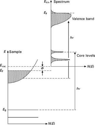
3.1 The left side of the figure shows energy levels in the crystal in the initial state. The photoemission process occurs with the absorption of a photon with energy hv. The right side of the figure shows the measured photoemission spectrum, starting from the vacuum level. From Damascelli et al. (2003).
To relate the relationship of the photoelectron momentum to the momentum of the photohole left in the crystal, we consider an electron in a crystal with a well-defined quasimomentum K, and energy EB. If the incident photon has enough energy to promote the electron above Evac, then the electron can be photoemitted into free space. Because the electron has to propagate a macroscopic distance (~1 m) to the detector, it can essentially be treated as a free plane wave with E = hk2/2 m. Therefore, by knowing the takeoff angles of the electron relative to the crystal axes and the detector, we can determine the momentum wavevector of the outcoming photoelectron. The geometrical considerations for the photoemission process are illustrated in Fig. 3.2. From this we can use momentum conservation to relate this to the quasimomentum of the electron in the initial state. We can roughly generalize the real situation to a semi-infinite crystal (infinite in the lateral directions, but with a discontinuous step – the crystal surface – in the z direction). In this case, the momentum in the lateral direction, kparallel is conserved due to translational symmetry, but the momentum in the z direction is clearly not conserved, owing to the work function step potential at the surface (the ‘lost’ kz momentum of the photoelectron across the barrier is then taken up by a recoil of the crystal). Therefore, we can obtain an exact measure of the in-plane wavevectors of the electron in the initial state, kparallel, but extracting kz is more challenging. To determine kz, one should determine the so-called ‘inner potential’ of the crystal, which is essentially determining which photoelectron kinetic energy corresponds to kz = 0 (the (0,0,0) point) (Hufner 1995). This is typically rather involved and requires spanning a wide range of incident photon energies, hv, in real measurements.
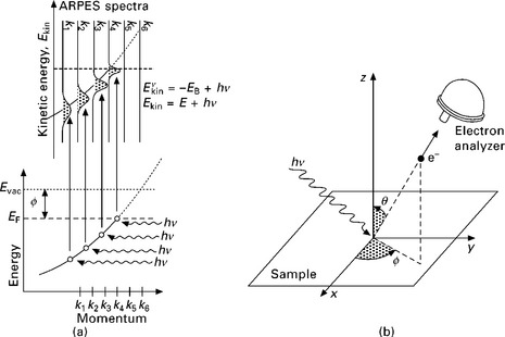
3.2 (a) Illustration of optical (direct) transitions from electrons in a band in the crystal, to photoelectrons in free space. (b) ARPES and measured observables, being photoelectron counts, photoelectron kinetic energy, and polar angles of photoelectron relative to sample crystal axes. From Damascelli et al. (2003).
It is generally most appropriate to view the experimentally measured photocurrent as a photoinduced transition between electron initial and final states. In UPS, the incoming photon carries negligible momentum (for hv = 10 eV, Q ~ 5 × 10− 3 A− 1), so all transitions are essentially direct, but this should clearly not be the case for XPS. To reach an available final state, the photoelectron should then be translated by a reciprocal lattice vector, G, so that the wavevector of the outgoing photoelectron K = k + G, demonstrating that the photoemission process requires the presence of a lattice potential to conserve momentum. The above analysis allows us to relate the photoelectrons measured at some kinetic energy and momentum to electrons with some different binding energy and momentum in the initial state, inside the crystal before the photoemission process. However, it does not tell us the direct relationship between the electronic states of the N and N–1 system. For this, one must make further assumptions beyond simple kinematics and conservation relations to obtain meaningful information about the N–1 system of the photohole from the experimentally measured photocurrent.
Rigorously speaking, the best theoretical description of the photoemission process is the so-called ‘one-step model’. In the one-step model, the photoemission process is treated as a single, entirely quantum-mechanical process. However, the phenomenological model which is nearly exclusively used in the experimental photoemission community is the ‘three-step’ model, popularized by Berglund and Spicer in 1964. The steps in the three-step model are as follows:
1. Optical excitation of the electron inside the solid.
The independent steps in the three-step model are shown in Fig. 3.3. In this semiclassical picture, only the first step is treated quantum mechanically, and the three steps are treated as independent of one another, in contrast to the correct quantum-mechanical one-step approach. The beauty of the three-step model is that it actually removes the complicated photoemission process itself from photoemission. The three-step model effectively reduces the photoemission process to an optical excitation. Steps (2) and (3) in the three-step model are simply attenuation factors and kinematic considerations, respectively, leaving (1) as the only nontrivial process. Given the dramatic simplifications of the three-step model, it works remarkably well and provides surprisingly accurate results.
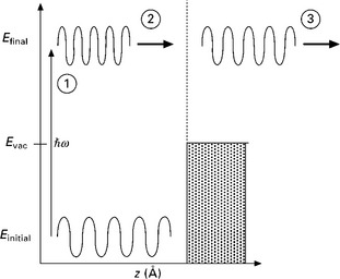
3.3 Illustration of the three-step model, with (1) optical excitation of an electron in the bulk, (2) transport of the photoelectron to the surface, and (3) escape of the photoelectron into vacuum free space.
Here we will discuss a few additional aspects of the photoemission process. First, photoemission is a highly surface-sensitive process because of the strong Coulomb interactions between the photoelectron and the rest of the electrons left in the solid, with a typical mean free path on the order of 1 nm for photon energies in the vacuum ultraviolet (VUV). Because the mean free path depends on the cross-section of the photoelectrons to scatter with plasmons, the mean free path should be even lower for ‘bad metals’ with low plasmon energies such as many strongly correlated transition metal oxides. This high degree of surface sensitivity is the reason for extremely stringent ultra-high vacuum conditions necessary for reliable, high-resolution ARPES experiments, and experiments are typically performed at pressures of better than 5 × 10− 11 torr. Samples are usually cleaved in situ at low temperatures and base pressure to ensure an atomically clean surface layer. Even at these pressures, we can occasionally observe surface degradation, although this varies significantly on the particular compound and contaminants in the vacuum chamber.
3.2.2 Instrumentation and light sources for high-resolution photoemission spectroscopy
ARPES experienced a renaissance in the late 1990s and early 2000s with the advent of 2D multiplexing analyzers by the Swedish company VG Scienta which could measure a range of electron kinetic energies and angles simultaneously. The way that traditional electron analyzers worked was that their angular acquisition was based on a small pinhole aperture. The position of the pinhole relative to the sample normal determined the photoelectron K, and the solid angle subtended by the pinhole determined ∆k. The problem with this approach is that all electrons outside this pinhole are discarded, and only one wavevector can be measured at a time. The great advantage of the Scienta analyzers is that the electron lens system for these analyzers allowed for parallel detection of many (~ 100) angular channels, thereby increasing the measurement efficiency by about two orders of magnitude. Today, such multiplexing analyzers are quite common and easily achieve energy resolutions of ∆E = 1 meV and simultaneously measure angular ranges greater than 30 degrees in parallel. The electrons pass through the entrance aperature, and then through a three-element lens system, through the entrance slits, and then the two concentric hemispheres housed inside the large stainless steel dome (all electron lens elements are electrostatic). The electrons are finally detected at the bottom of the analyzer, after the electron signals are amplified by a pair of microchannel plates (MCPs) and a phosphor screen. Flashes on the phosphor screen are then detected ex situ by a CCD camera looking through the window, visible at the bottom flange. An illustration of a Scienta analyzer operating at a synchrotron beamline is shown in Fig. 3.4.
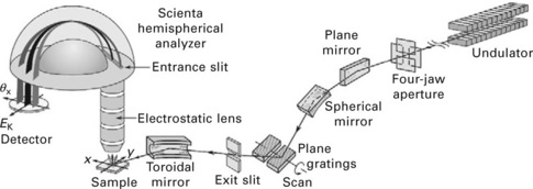
3.4 Schematic of Scienta analyzer on a beamline. Photoelectrons with different take-off angles are imaged onto the long entrance slit, and pass through the concentric hemispheres, and strike the microchannel plates. From Damascelli et al. (2003).
A major barrier to performing UPS is the relative dearth of appropriate UV and VUV photon sources. As a result, many UPS and ARPES systems are located at synchrotrons where at undulator insertion devices, tunable photon energies can be achieved with high photon fluxes (~ 1012 photons/s mm2) within a narrow (~ meV) energy bandwidth. Synchrotron sources remain the light source of choice for ARPES, as no other sources can match their flexibility in terms of photon energies and polarizations. However, because of the scarcity and relatively small number of synchrotrons, laboratory-based UV and VUV sources present a highly desirable alternative. These sources must exceed the energy of the work function (typically 4–5 eV), and such light sources are relatively scarce. The most common light sources for laboratory- based UPS are plasma discharge (He, Ar, Xe) lamps which have discrete emission lines with high brightness (~ 1012/s mm2) and narrow spectral widths (~ 1 meV). The main disadvantage to plasma discharge lamps is the lack of tunability in photon energies which can be essential for many experiments. More recently, VUV lasers which use higher harmonic generation (HHG) have come to the forefront. Although currently restricted in photon energy tunability and limited to fairly low photon energies (5–7 eV), they have the distinct advantage of superior spectral linewidths and brightness over plasma discharge lamps. In addition, laser sources can be utilized for time-resolved experiments such as pump-probe measurements. However, at present, the wavelengths available to VUV lasers is rather restricted, although this is likely to change as the technology matures.
3.3 Applications of UPS to thin film systems
3.3.1 SrRuO3
SrRuO3 has drawn wide interest for thin film studies and applications for a number of major reasons. First, SrRuO3 is a ferromagnetic metal (Tc = 160 K) which is unusual for a 4d transition metal oxide, but also exhibits unconventional ‘bad metal’ behavior at elevated temperatures. The Ruddlesden-Popper series of layered ruthenates Srn + 1RunO3n + 1, of which SrRuO3 is the three-dimensional end-member, display a remarkable evolution in magnetic and electronic properties as a function of dimensionality, n. The single layer n = 1 compound, Sr2RuO4, is an exotic spin triplet superconductor with a time- reversal symmetry breaking ground state (Mackenzie and Maeno 2003). The n = 2 bilayer compound, Sr3Ru2O7 exhibits quantum critical metamagnetism and an apparent electronic nematicity where the magnetoresistance breaks C4 symmetry (Borzi et al. 2007). Ferromagnetic tendencies are enhanced by increasing the number n of RuO2 sheets per unit cell. In addition, Ca substitution for Sr dramatically alters the magnetic and electronic properties of all known members of the Srn + 1RunO3n + 1 ruthenates, despite the fact that Ca and Sr are isovalent (for instance, CaRuO3 is a paramagnetic metal, and Ca2RuO4 is an antiferromagnetic insulator). In addition, spin–orbit interactions and 4d orbital degeneracies are known to be important factors. Therefore, SrRuO3 and other members of the ruthenate family present a wealth of exotic electronic and magnetic behaviors which are ripe for investigation. From the thin film standpoint, SrRuO3 is also an excellent material for investigation since epitaxial thin films of very high quality can be synthesized. Until very recently, many properties of films (such as resistivity) were found to exceed even those of the best bulk single crystals. In addition, the low resistivity of SrRuO3 films make it an excellent candidate material for thin film applications such as electrode materials or magnetic tunnel junctions. In addition, the pseudocubic perovskite structure makes SrRuO3 suitably lattice matched to other common transition metal oxides such as SrTiO3, a common substrate material for SrRuO3.
Because the electronic properties of SrRuO3 are still not well understood, UPS and ARPES studies of SrRuO3 are essential for answering important basic questions about the electronic structure, such as whether first-principles calculations can capture an accurate description of this complex correlated material which exhibits ferromagnetism and three-fold orbital degeneracy, or the nature of the large effective masses and the strength of electron–electron correlations. However, because of its pseudocubic structure, cleaving single crystals does not yield the flat, well-defined surfaces necessary for ARPES. Therefore, measurements of atomically flat thin film samples synthesized in situ are essential for performing ARPES measurements of the quasiparticle band structure and Fermi surface. Moreover, because of the surface sensitivity of the ARPES technique (inelastic mean free path ~ 1 nm), these thin film samples cannot be removed from ultra-high vacuum (UHV) conditions before measurement; exposure of an atomically pristine surface to atmosphere can render a surface unmeasurable within nanoseconds. Therefore, the synthesis, transfer, and measurement stages must all take place under strict UHV conditions.
The earliest UPS measurements of SrRuO3 were performed by Fujioka et al. (1997) and Okamoto et al. (1999) on polycrystalline samples of SrRuO3 which were sintered as pellets and scraped in situ. Based on comparisons to the density of states obtained from band structure calculations, Okamoto et al. were able to obtain a mass enhancement factor of approximately m*/mb ~ 4.4, which appeared consistent with estimates from transport measurements. On the other hand, based on this analysis, it is difficult to determine the origin of this fairly large mass enhancement, although it has been speculated by Fujioka et al. that this may be due to electron–electron interactions. On the other hand, Mazin and Singh (1997) have argued that electron–magnon and phonon couplings in SrRuO3 could be anomalously large due to the important role of oxygen in forming the ferromagnetic state. A major limitation of performing photoemission spectroscopy on polycrystalline samples is the lack of any momentum-resolved information. Therefore, developing a method for pursuing in situ photoemission studies of SrRuO3 thin films will be critical for in-depth studies of the electronic structure of SrRuO3.
Using a novel combination of both PLD and MBE, Siemons et al. (2007) were able to synthesize a variety of SrRuO3 thin films with varying degrees of Ru stoichiometry and quantified the strong dependence of the Ru stoichiometry (deficiency) on the unit cell volume and c-axis lattice constant as well as with the residual resistivity ratio (RRR), as shown in Fig. 3.5. They determine that films grown by PLD are typically ruthenium deficient with poor (low) residual resisitivities and can have an expanded unit cell volume, and could synthesize thin films with RRRs as low as 5 or less (PLD, high oxygen pressures) or up to 40 (MBE, low oxygen pressures). It is interesting to note that the Curie temperature is only very weakly dependent on Ru stoichiometry, and therefore should not be used as a metric for determining the quality of SrRuO3 thin films. In addition, using in situ photoemission spectroscopy, Siemons et al. clearly demonstrate that the quality of the UPS spectra of these thin films near EF (E < 1 eV) is strongly dependent on the Ru stoichiometry. In particular, the spectral intensity near EF (constituted primarily of the Ru dxy, dyz, and dxz orbitals) is strongly suppressed with respect to the background at higher binding energies as shown in Fig. 3.6. Therefore, measurements which attempt to extract the quasiparticle mass enhancement based solely on comparisons of spectral weight intensities and comparisons with theoretical densities of states must necessarily take into account the potentially sizable effects of Ru non-stoichiometry on the photoemission spectra.
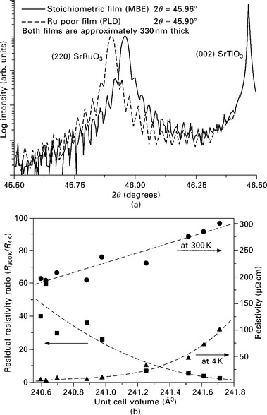
3.5 Characterization of the dependence of (a) the c-axis lattice constant and (b) the resistivity and residual resistivity ratio (R300 K/R4 K) on the Ru stoichiometry of SrRuO3 thin films grown by PLD and MBE, as characterized by Siemons et al. (2007).
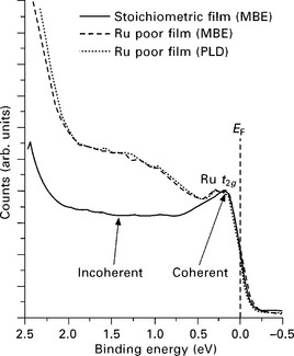
3.6 Dependence of the near EF spectral weight on the Ru stoichiometry in thin films of SrRuO3 as measured by in situ UPS using a He I discharge lamp. From Siemons et al. (2007).
As mentioned earlier, the electronic and magnetic properties of the Ruddlesden–Popper series ruthenates are known to depend critically on dimensionality. In response to this, ultrathin films of SrRuO3 grown on SrTiO3 have been investigated and an evolution in their electronic and magnetic properties have been reported by increasing the SrRuO3 film thickness within the first 10 monolayers (MLs) of growth. Xia et al. (2009) have determined through a combination of polar Kerr effect measurements and resistivity that below a SrRuO3 film thickness of 4 MLs, the material’s ferromagnetic properties appear to be heavily suppressed, suggesting the formation of antiferromagnetism, while above 4 MLs, bulk-like behavior is reported. In conjunction with this ferromagnetic suppression, films thinner than 4 MLs exhibited insulating behavior in resistivity measurements, shown in Fig. 3.7. These findings are consistent with earlier reports by Toyota et al. (2005) which studied the evolution of the photoemission spectra of SrRuO3 films as a function of thickness. As shown in Fig. 3.8, below approximately 6 MLs, there is little to no spectral intensity near EF, while above 10 MLs the spectra are similar to much thicker (100 ML) films. This again points to some kind of metal–insulator transition around 4 MLs which also appears to be coincident with a dramatic change in the ferromagnetic properties of the material.
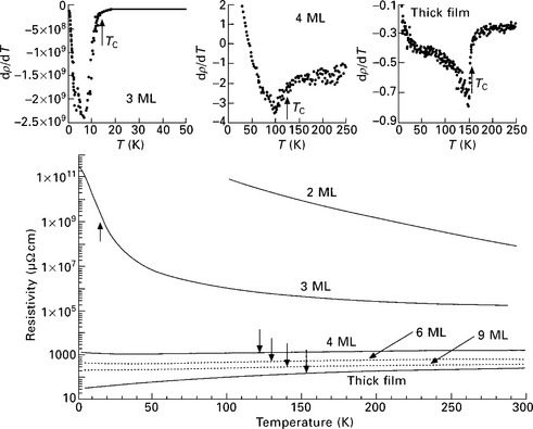
3.7 Resistivity of SrRuO3 films showing the dependence of the resistivity and the ferromagnetic transition on the film thickness in monolayer (ML). From Xia et al. (2009).
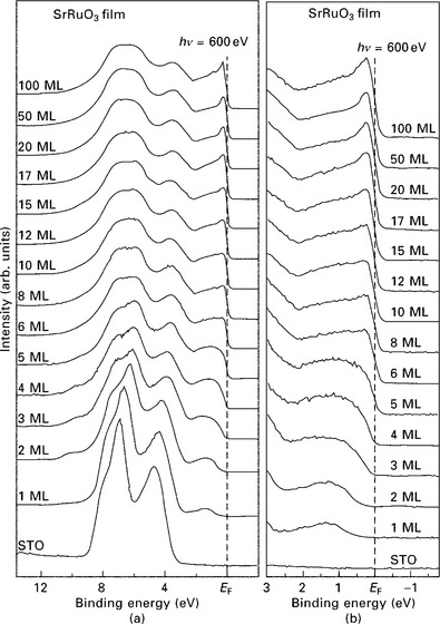
3.8 In situ photoemission valence band spectra of SrRuO3 grown by PLD as a function of nominal film thickness, showing depleted spectral weight near EF below 5 ML. From Toyota et al. (2005).
The work by Siemons and Toyota clearly establishes the importance of in situ photoemission spectroscopy on uncovering the complex electronic structure of SrRuO3. However, there is still much to be learned about the underlying electronic structure which may come from future angle-resolved measurements as well as additional thickness dependence studies of ultrathin SrRuO3 films. At present, angle-resolved photoemission measurements of SrRuO3 have not yet been conducted, although these recent successes of in situ angle-integrated photoemission measurements on SrRuO3 and in situ ARPES on other thin films such as La1–xSrxMnO3 suggest that future ARPES measurements on SrRuO3 films are not far off on the horizon. ARPES measurements will be key in answering critical questions about the intrinsic electronic structure of SrRuO3, such as whether density functional theory can adequately predict the electronic structure of such a complex, correlated multi-band ferromagnet, or what is the true nature (electron–electron or electron–boson coupling) of the large mass renormalization observed in SrRuO3. However, a major consideration will be that accounting for Ru stoichiometry will be particularly critical for high-quality ARPES measurements. A high concentration of Ru vacancies will introduce a large amount of scattering which would broaden and mix otherwise well-defined eigenstates in momentum space, meaning the materials requirements for ARPES will be even more stringent than for angle-integrated UPS.
3.3.2 La1–XSrXMnO3
The Re1–xAexMnO3 manganites (with Re a rare earth, and Ae an alkaline earth metal) have been at the forefront of the field of strongly correlated electrons due to their host of electronic phases and dramatic phase transitions. Most well known amongst these properties is colossal magnetoresistance (CMR), where the electrical resistance can drop by more than six orders of magnitude with the application of a magnetic field. La1–xSrxMnO3 (LSMO) shows excellent metallic behavior and the highest Curie temperature of all Re1–xAexMnO3 variants, and is predicted theoretically to be 100% spin polarized. Based on these properties, LSMO is a potentially ideal material for the development of new spintronics devices, particularly magnetic memory and magnetic sensors. Toward this end, CMR effects in LSMO tunnel junctions and the integration of semiconductors into LSMO-based devices have been demonstrated, and a great deal of interest and work has been devoted to synthesizing epitaxial thin films of LSMO and other manganite compounds. Recently, there has also been great activity in using LSMO as a building block for novel heterostructured materials. Cation-ordered versions of LSMO, where layers of LaMnO3 are alternately stacked with layers of SrMnO3, have shown new and dramatic metal–insulator transitions, increased ordering temperatures, and may generate spin-polarized two-dimensional electron gases at the LaMnO3–SrMnO3 interfaces.
Due to its three-dimensional pseudocubic structure, ARPES measurements of bulk single crystals of LSMO remain inaccessible because of the inability to produce a well-defined crystallographic surface upon cleaving. Therefore, like the case of SrRuO3, atomically flat thin film samples of LSMO grown in situ using MBE or PLD provide the only route to accessing the electronic structure of these materials. The importance of understanding the complex electronic structure of this strongly correlated material has led to various research groups performing in situ ARPES studies of thin films of LSMO.
The first in situ ARPES studies of thin films of LSMO were reported by Shi et al. (2004) and later by Chikamatsu et al. (2006). Thin films were synthesized using pulsed laser deposition on SrTiO3 substrates. Measurements were conducted using an energy resolution of 150 meV and an angular resolution of 0.5° for the work of Chikamatsu et al. and 40 meV and 0.2° for Shi et al. Chikamatsu et al. demonstrated for x = 0.4 that the valence band (within ~ 10 eV of the Fermi level) exhibits generally good agreement with band structure calculations based on a local density approximation plus on-site Coulomb interactions (LDA + U), shown in Fig. 3.9. Close to EF (within 1 eV), only broader features with weak spectral weight could be observed near EF. While the approximate dispersion of these features qualitatively tracked some of the LDA + U predictions, important questions persist about the nature of these near EF states. First, the reason for the dramatically reduced near EF spectral weight is still unclear, although it has been suggested that this spectral weight suppression could be the signature of polaronic behavior due to strong electron–phonon interactions, shown in Fig. 3.10. However, it may be conceptually challenging to reconcile small polaron formation (and subsequently very large effective masses) with its reasonably metallic behavior at low temperatures (ρ ~ 10− 5 Ω cm).
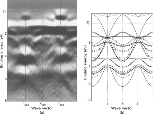
3.9 In situ ARPES measurements of the valence band of La1.6Sr0.4MnO3 thin films, showing the (a) second-derivative plots of the valence band and (b) band structure calculations using the local density approximation plus on-site Coulomb interactions (LDA + U). Solid and dashed lines correspond to spin majority and minority bands respectively. From Chikamatsu et al. (2006).
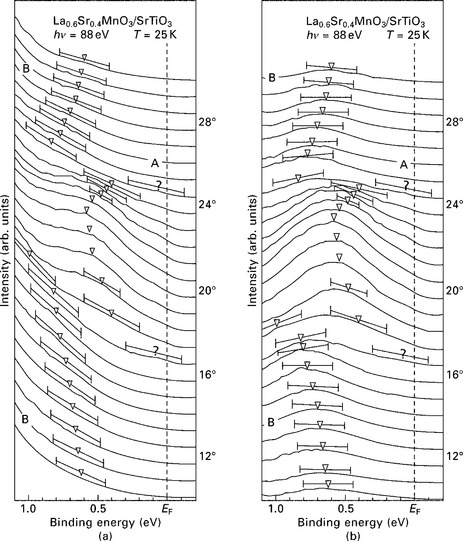
3.10 ARPES measurements of the near EF spectra of La1.6Sr0.4MnO3 thin films enlarged around the G (k = (0,0,0)) point. The open symbols represent the approximate energy positions of possible dispersive features. Panel (a) shows raw data; panel (b) shows data after subtraction of a high binding energy background. 'A' denotes the dispersive low energy band, while 'B' denotes the weakly dispersive high energy feature. From Chikamatsu et al. (2006).
The work by Shi et al. on films of x = 0.33 grown by PLD also revealed that the large-scale electronic structure in the valence band also agreed reasonably well with predictions, but similar to the work by Chikamatsu et al., the near EF electronic structure remained somewhat surprising. In particular, in both Chikamatsu’s and Shi’s works, a large sheet of Fermi surface predicted by theory (a large hole-like cubic sheet centered at k = (π,π,π)) was experimentally absent. Shi et al. have suggested that strong nesting between the flat faces of this sheet could have resulted in a charge density wave instability that results in this Fermi surface being entirely gapped. While a distinct possibility, such nesting driven density wave instabilities are highly uncommon in three-dimensional compounds due to phase space considerations, as pointed out by Chikamatsu et al.
At present, the origin of the apparent discrepancy between theory and experiment for these near EF states in LSMO is still unclear. Because it is the states near EF that are responsible for the thermodynamic properties, determining the electronic structure of these states and the suitability of theory to describe these materials remains a critical issue. In addition, LSMO is a polar compound, and charge redistribution at the surface which could alter the doping level on the surface relative to the bulk is another potential source of the discrepancy between experiment and theoretical predictions. At present, the possibilities regarding this apparent disagreement are as follows: whether this is due to (1) a failure of the density functional theory caused by the presence of strong electron correlations and magnetism, (2) the presence of a competing density wave instability which gaps out parts of the Fermi surface, (3) an altered surface electronic structure caused by the polar redistribution of charge and the surface termination, (4) strong electron–phonon interactions which dramatically suppress the near-EF spectral weight resulting in highly massive polaronic charge carriers, or some combination of these various factors.
These first ARPES experiments have clearly demonstrated the importance and feasibility of thin film studies of LSMO and other closely related manganite perovskites. These measurements clearly demonstrate that the high energy structure of the valence band agrees well with predictions based on density functional theory, but clear discrepancies exist between the theory and experiment regarding the Fermi surface and near EF band structure which are still unresolved. Therefore important questions remain which must be resolved before a clear understanding of the electronic structure of LSMO can be achieved through future ARPES experiments on LSMO thin films.
3.4 Future trends
The examples discussed in this chapter demonstrate the clear feasibility of performing in situ UPS on thin films. At present, we are only beginning to scratch the surface of what high-resolution angle-resolved UPS can achieve in revealing the electronic structure and many-body interactions in thin film samples. As described in this chapter, one major application of UPS and ARPES on in situ film samples is studying materials which do not have a natural cleavage plane, but which can be grown as atomically flat samples.
However, the next frontier in thin film materials is the design and discovery of new electronic materials at atomically abrupt interfaces between different correlated materials. While a great deal of work is currently underway in synthesizing interfacial electronic matter at oxide interfaces, these electronic states are extremely difficult to access using bulk probes. Hence, little is understood about the true electronic structure of these interfacial electronic states. ARPES and UPS are poised to play a key role in the study of in situ correlated interfaces, where the surface sensitivity of photoemission may be a double-edged sword. On the one hand, photoemission can be highly sensitive to the electronic states in a single monolayer, making it highly suitable for studying interfacial states. On the other hand, photoemission will have difficulty accessing interfaces which are deeply buried (more than 1–2 nm) below the surface. Along these lines, the development of more bulk-sensitive photoemission techniques, for instance by employing very low (hv < 10 eV) or high (hv > 1 keV) energy photon sources which increase the electron mean free path, may be critical for studying deeply buried interfaces. Bulk-sensitive photoemission will also be crucial for disentangling the surface and bulk electronic structures of materials which have a highly three-dimensional structure, like the examples provided in this chapter.
3.5 References
Berglund, C.N., Spicer, W.E. Photoemission studies of copper and silver. Phys. Rev. A. 1964; 136:1030.
Borzi, R.A., Grigera, S.A., Farrell, J., Perry, R.S., Lister, S.J.S., Lee, S.L., Tennant, D.A., Maeno, Y., Mackenzie, A.P. Formation of a nematic fluid at high fields in Sr3Ru2O7. Science. 2007; 315:214.
Chikamatsu, A., Wadati, H., Kumigashira, H., Oshima, M., Fujimori, A., Hamada, N., Ohnishi, T., Lippmaa, M., Ono, K., Kawasaki, M., Koinuma, H. Band structure and Fermi surface of La0.6Sr0.4MnO3 thin films studied by in situ angle-resolved photoemission spectroscopy. Phys. Rev. B. 2006; 73:195105.
Damascelli, A., Hussain, Z., Shen, Z.X. Angle-resolved photoemission studies of cuprate superconductors. Rev. Mod. Phys. 2003; 75:473.
Fujioka, K., Okamoto, J., Mizokawa, T., Fujimori, A., Hasi, I., Abbate, M., Lin, H.J., Chen, C.T., Takeda, Y., Takano, M. ‘Electronic structure of SrRuO3’, Phys. Rev B. 1997; 56:6380.
Hufner, S. Photoelectron Spectroscopy: Principles and Applications. New York: Springer-Verlag; 1995.
Kane, E.O. Implications of crystal momentum conservation in photoelectric emission for band structure measurements. Phys. Rev. Lett. 1964; 12:97–98.
Kiss, T., Shimojima, T., Ishizaka, K., Chainani, A., Togashi, T., Kanai, T., Wang, X.Y., Chen, C.T., Watanabe, S., Shin, S. A versatile system for ultrahigh resolution, low temperature, and polarization dependent laser-angle-resolved photoemission spectroscopy. Rev. Sci. Inst. 2008; 79:023106.
Mackenzie, A.P., Maeno, Y. The superconductivity of Sr2RuO4 and the physics of spin-triplet pairing. Rev. Mod. Phys. 2003; 75:657.
Mazin, I.I., Singh, D.J. Electronic structure and magnetism in Ru-based perovskites. Phys. Rev. B. 1997; 56:2556.
Okamoto, J., Mizokawa, T., Fujimori, A., Hase, I., Nohara, M., Takagi, H., Takeda, Y., Takano, M. Correlation effects in the electronic structure of SrRuO3. Phys. Rev. B. 1999; 60:2281.
Shi, M., Falub, M.C., Willmott, P.R., Krempasky, J., Herger, R., Hricovini, K., Patthey, L. k-dependent electronic structure of the colossal magnetoresistive perovskite La0.66Sr0.34MnO3. Phys. Rev. B. 2004; 70:140407.
Siemons, W., Koster, G., Vailionis, A., Yamamoto, H., Blank, D.H.A., Beasley, M.R. Dependence of the electronic structure of SrRuO3 and its degree of correlation on cation off-stoichiometry. Phys. Rev. B. 2007; 76:075126.
Toyota, D., Ohkubo, I., Kumigashira, H., Oshima, M., Ohnishi, T., Lippmaa, M., Takizawa, M., Fujimori, A., Ono, K., Kawasaki, M., Koinuma, H. Thickness-dependent electronic structure of ultrathin SrRuO3 films studied by in situ photoemission spectroscopy. Appl. Phys. Lett. 2005; 87:162508.
Traum, M.M., Smith, N.V., DiSalvo, F.J. Angular dependence of photoemission and atomic orbitals in the layer compound 1 T-TaSe2. Phys. Rev. Lett. 1974; 32:1241.
Xia, J., Siemons, W., Koster, G., Beasley, M.R., Kapitulnik, A. Critical thickness for itinerant ferromagnetism in ultrathin films of SrRuO3. Phys. Rev. B. 2009; 79:140407(R).