
Inelastic scattering techniques for in situ characterization of thin film growth: backscatter Kikuchi diffraction
Abstract:
The inherent characteristics of electron diffraction are particularly useful for determining the full structure (lattice parameters, space group, atomic positions) of thin films in situ and in real-time. Electrons are easy to generate, manipulate, and detect, and they have a strong interaction with matter. However, the dynamic nature of electron diffraction generally makes detailed analysis complicated. Along with the multiple scattering complications comes one significant benefit: the formation of Kikuchi diffraction patterns. These contain within them a representation of the full three-dimensional structure of the probed material.
2.1 Introduction
The geometrical constraints within a molecular beam epitaxy (MBE)-like deposition chamber, and the small quantity of material available for study, make determining the full structure (lattice parameters, space group, atomic positions) of a thin film in situ and in real-time a serious challenge. The inherent characteristics of electron diffraction are particularly useful for approaching this problem. Electrons are easy to generate, manipulate, and detect, and they have a strong interaction with matter. However, the dynamic nature of electron diffraction generally make its detailed analysis complicated. There is a significant benefit to the multiple scattering complications: the formation of Kikuchi diffraction patterns, which contain a representation of the full three-dimensional structure of the probed material.
Kikuchi diffraction patterns are the result of diffraction from inelastically scattered electrons, and they can be found when using all electron diffraction techniques. They are used most widely in transmission electron microscopy (TEM) and scanning electron microscopy (SEM) as techniques for tracking the orientation of a crystal structure in space. It is convenient to think of these Kikuchi patterns as being generated from a point source of electrons located within the diffracting medium; and doing so provides a framework for understanding their simultaneous access to all of the diffraction planes in a sample. This leads to data-intensive, complex, and rich diffraction patterns. The access to all of a sample’s diffraction planes, and the ease of collecting this type of diffraction pattern, makes it a potentially invaluable tool for the in situ and real-time characterization of thin films.
2.2 Kikuchi patterns
In the 1920s, while studying thin mica films using an electron beam, S. Kikuchi (1928) observed a background structure, as well as the expected diffraction peaks, up to 20° away from the direction of the beam. This background structure consisted of a series of parallel line pairs, later called Kikuchi lines. Kikuchi developed a fairly straightforward interpretation of these lines, often referred to as the ‘two-event model’. In this model the incoming collimated and mono-energetic beam of electrons are diffused in the crystal by an unspecified scattering process. In essence, this first step generates a source of electrons traveling in multiple directions, inside the material. The second step is then standard Bragg diffraction of the diffused electrons from the planes in the material.
From any point inside the crystal there are two possible angles for which Bragg diffraction from a single set of lattice planes can occur. Therefore, each set of crystallographic planes generates two diffraction cones with a large opening angle of 180° – 2θhkl and an axis perpendicular to the diffracting lattice planes. These cones will be seen on a collecting screen as a pair of lines, i.e. the Kikuchi lines (see Fig. 2.1). These lines will be parallel to, and on either side of, the intersection of the diffracting lattice plane with the screen. In reality, the multiple scattering process required to generate Kikuchi patterns leads to more complex contrasts in the image than simple pairs of lines (Reimer, 1985). The diffraction pattern is better described as bands with excess or deficient Kikuchi lines that define the edge of the band.
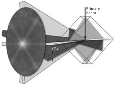
2.1 A schematic of the Kikuchi band formation highlighting the Kikuchi band’s connection to the lattice planes.
Several years after Kikuchi had observed Kikuchi patterns in transmission, transmission Kikuchi patterns (TKPs), the same types of patterns – consisting of parallel line pairs – were observed up to 160° from the incoming beam of electrons (von Meibom and Rupp, 1933; Boersch, 1937). These patterns are now described as backscatter Kikuchi patterns (BKP). Although the phenomenological ‘two-event model’ description of the formation of the TKP and BKP are similar and the geometrical interpretation of the patterns are identical, there has been debate as to whether the same mechanisms are involved in TKP and BKP formation due to the large difference in scattering angles (Alam et al., 1954; Reimer, 1985; Wells, 1999; Zaefferer, 2007).
Simulations that use thermal diffuse scattering as the primary process of incoherent and inelastic scattering agree quite well with experimental TKPs (Omoto et al., 2002). Recently it has also been argued that because of the lower primary beam energies used to generate BKPs, the same thermal diffuse scattering can also account for the large scattering angles in BKP formation (Zaefferer, 2007).
2.2.1 Tem
TEM relies heavily on TKP patterns to help determine the orientation and tilt axis of a sample in the microscope. This is primarily due to the fact that the Kikuchi patterns are an image of the real crystal symmetry and therefore behave as if attached to the crystal, i.e. they provide a continuous pattern that moves in the same sense as the crystal. This allows a Kikuchi map to be used as a roadmap for moving around reciprocal space. This can be advantageous for stereomicroscopy, contrast work, and selected area diffraction alignment (Gareth, 1979).
TKPs also provide a means for general structure analysis in TEM, including structure and phase identification, grain boundary mapping, and texture mapping. Convergent beam electron diffraction, generally referred to as CBED, provides access to the symmetry of the crystal and to the position of atoms within the unit cell, on crystals down to about 2 nm in size. CBED is inherently a dynamic diffraction problem, and as such the presence of Kikuchi bands within the diffraction pattern are a significant part of the CBED pattern analysis (Omoto et al., 2002).
2.2.2 Sem
There has been a great deal of interest in BKP within the materials science community because of its usefulness in studying texture and orientation relationships on a micron length scale in SEM (see, for example, Venables et al, 1976; Dingley et al, 1989; Dingley and Randle, 1992; Randle, 1992; Field, 1997; Dingley, 2004). In this style of work, the electron beam is scanned over a sample and BKPs are collected at each point in the scan. Crystallographic orientational changes from one area in the sample to the next are then easily identified as a change in the BKP, thereby generating a map of the grain structure. This technique is normally called electron backscatter diffraction (EBSD). In addition to this work on orientational mapping, EBSD patterns collected from an SEM have also been used for phase identification by crystallographic point group or space group classification, even on nanoparticles (Baba-Kishi and Dingley, 1989a, 1989b; Dingley et al., 1995; Small et al., 2002), and the evaluation of both plastic and elastic strains (Troost et al., 1993; Wilkinson, 1996).
The angular dependent variations seen in the backscatter electron yield in SEM, called electron channeling patterns (ECPs), are very similar to the EBSD patterns, and it has been suggested that the ECPs and EBSD patterns are theoretically related by the reciprocity theorem (Venables and Harland, 1973; Reimer, 1985).
2.2.3 Kikuchi pattern analysis
A Kikuchi pattern is, in essence, a gnomonic projection of the intersection of all the sample’s lattice planes with a sphere of reflection centered on the electron source point (see Fig. 2.1). As such, the intersection of different Kikuchi lines indicates the location of a zone axis, and displays the symmetry of the zone axis. Based on these ideas, general procedures have been developed for using a BKP (or TKP) to determine the unit cell and space group of a sample (Baba-Kishi and Dingley, 1989a, 1989b; Dingley et al., 1995; Dingley and Wright, 2009).
The analysis of the BKP to obtain space group information starts with the analysis of individual zone axes (i.e. points where at least two sets of Kikuchi lines cross), in order to define their respective point group symmetries (see Fig. 2.2). Since the BKP does not distinguish between point groups with and without the inversion symmetry, there are only 11 possible symmetries to be considered. These symmetries are the so-called Laue groups. The combination of the laue groups from several zone axes will then allow the determination of the crystallographic point group (see Table I from Baba-Kishi and Dingley, 1989a, or Dingley et al., 1995). From this point on, determining the space group requires the ability to calculate some rough lattice parameters from the ratios of the d-spacings and interzonal angles of the principal reflections, then simulate the BKP, and finally test the resulting match to the experimental pattern. With some a priori knowledge of the Bravais lattice, this procedure can be fully automated with band detection algorithms based on the Hough transformation (Lassen et al., 1992; Schwarzer, 1997). This automation is possible using most commercial EBSD software packages.
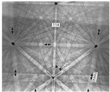
2.2 BKP from a cleaved (001) crystal of silicon at 40 kV with crystallographic symmetry marked on several zone axes. Reprinted with permission (Baba-Kishi, 2002).
It is worth highlighting that Kikuchi pattern formation is inherently a multiple scattering phenomenon, which can influence the intensity comparison between the experimental patterns and simulated patterns based on kinematic theory.
2.3 Kikuchi lines in reflection high-energy electron diffraction (RHEED) images
In addition to coherent Bragg diffraction, reflection high-energy electron diffraction (RHEED) images generally also include a diffuse background, sharp Kikuchi lines, and surface resonance features (see Fig. 2.3a). These additional features are generally spectroscopically separated from the coherent Bragg diffraction peaks (Horio et al., 1996; Staib et al., 1999; Nakahara et al., 2003), and energy filtering can remove them.
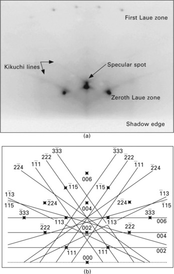

2.3 (a) An exemplary RHEED image with the shadow edge, specular spot, Laue zones and Kikuchi lines identified. (b) Theoretical Kikuchi line pattern for the crystal surface geometry of a face centred cubic (fcc) (001) surface along the [110] direction. No surface potential corrections are included. (c) Kikuchi line fits to the diffraction patterns of GaAs (001) β (2 × 4) reconstructed surface, which include the surface potential. The arrows indicate the most reliable points for fitting. Reprinted with permission (Ingle et al., 2010), Reprinted with permission (Braun et al., 1998b), Reprinted with permission (Braun et al., 1998a)
The Kikuchi patterns found in RHEED images can be quite sharp and contain significant intensity in the case of crystals with very high bulk and surface order. As with TKP in the TEM, the Kikuchi patterns seen on the RHEED screen are easily distinguishable from the coherent Bragg diffraction intensity because they move in a continuous and coincident manner when the crystal is rotated. Because of this, they can be used to align the azimuthal direction of the sample with respect to the incoming electron beam with high accuracy.
A simple reciprocal lattice-based method can be used to describe the expected locations of Kikuchi lines on the RHEED screen (Dobson, 1988; Gajdardziska-Josifovska and Cowley, 1991; Braun, 1999; Ichimiya and Cohen, 2004). After the first step of the two-event model has occurred – the inelastic scattering step – electrons will be traveling in all directions within the crystal. These electrons then scatter, with conservation of energy and momentum, in the second step. This requires that both the incident (k0) and the scattered wavevector (k) for the second step of the two-event model have equal magnitudes and that the scattering vector (k – k0) be a vector in the reciprocal lattice (g). Mathematically this can be written as 2k0 · g + g2 = 0, which when drawn for all possible k0 vectors produces the Brillouin zone boundaries for the given reciprocal lattice. Therefore, to identify the Kikuchi patterns seen in the RHEED image for any particular azimuthal direction, we must first plot the reciprocal lattice points perpendicular to that direction, and then the perpendicular bisectors of those reciprocal lattice points, i.e. the Brillouin zone boundaries, can be drawn (see Fig. 2.3(b)). This will produce all the possible geometries of the Kikuchi lines, although far fewer lines will be seen in practice.
The grazing angles of the scattered electrons that form the Kikuchi patterns in the RHEED image lead to several significant effects. The first is that the sample’s surface potential strongly alters the perpendicular momentum of the scattered electrons in this geometry, causing the Kikuchi lines to become curved (see Fig. 2.3(c)). This refraction effect has been used by Braun (Braun et al., 1998a; Braun, 1999) to quantitatively determine the surface potential needed for further dynamic scattering calculations. Braun was also able to extract the mis-orientation of a sample’s surface with respect to the underlying crystallographic orientation (i.e. the sample miscut) from fitting the RHEED-based Kikuchi patterns (Braun, 1999). In addition, the presence of terraces on a surface can change the behavior of the refraction depending on whether an electron leaves the surface through the edge of a terrace, or through the terrace surface (Dobson, 1988). The final effect is that the electrons that generate these grazing angle Kikuchi patterns are expected to originate primarily from the near surface region, and therefore may not generate Kikuchi patterns that are representative of the bulk. Kikuchi patterns for two-dimensional structures have been determined and evidence found in the annealed and reconstructed MgO (111) surface (Gajdardziska- Josifovska and Cowley, 1991) and a vacuum cleaved GaAs (110) surface (Braun, 1999).
One additional complication associated with the presence of Kikuchi patterns in the RHEED image is that there can be significantly enhanced intensity where the Kikuchi patterns and the coherent Bragg diffraction patterns overlap. This effect is called a surface-wave resonance (Wang, 1996), and can lead to an order of magnitude increase in the intensity at these locations.
Baba-Kishi (1990) collected RHEED images within an SEM, allowing a geometry and beam energy that could collect electrons over a much wider angular range than is standard for RHEED measurements. Figure 2.4 shows the RHEED pattern collected at 40 keV from a (100) surface of GaAs. Close to the pattern center, where the contrast has been adjusted to allow features to be seen, the white arrows indicate enhanced intensity from the surface-wave resonance where the Kikuchi lines overlap with the coherent Bragg diffraction. Close to the white arrows, the Kikuchi patterns that are commonly found in RHEED images are clearly evident. Moving radially out from the center of the pattern, it is possible to observe that the Kikuchi lines normally seen in the RHEED images are the excess Kikuchi lines on one side of the Kikuchi bands that are present in BKP and TKPs. On stepping further out, there is a sharp continuous circle of intensity which is called a high-order Laue zone (HOLZ) ring. The excess Kikuchi lines which form the envelope of the HOLZ rings become bright when the deficient Kikuchi lines are close to the zone axis. The diameter of HOLZ rings is related to the distance between atoms in a zone-axis direction, and has been used by Michael and Eades (2000) to determine lattice parameters. Beyond the HOLZ rings, the Kikuchi bands become the more familiar BKPs.
2.4 RHEED and Kikuchi pattern obtained at 40 keV from a (100) surface of single-crystal GaAs. Reprinted with permission (Baba- Kishi, 1990).
The combination of intensity from both coherent and incoherent scattering processes in the RHEED image complicates quantitative analysis because it requires a unified treatment within the dynamical high-energy diffraction theory (Winkelmann, 2010). This problem has been studied for CBED because coherent diffraction, HOLZ rings, and Kikuchi patterns are simultaneously present (Cowley, 1995; Omoto et al., 2002). Collecting Kikuchi patterns away from coherent scattering allows for greater ease of interpretation and modeling.
2.4 Dual-screen RHEED and Kikuchi pattern collection
Kikuchi patterns, generated by the RHEED electron gun, are present in the full hemisphere above the sample surface. Horio (2006) investigated the combination of RHEED and Kikuchi patterns on a Si(111)-7×7 surface using a conventional RHEED set-up and a second hemispherical screen in line with the sample normal. This hemispherical screen (see Fig. 2.5(a)), which led to the name astrodome RHEED, was used to enable an acceptance angle of 95°; it also minimized the distortion of Kikuchi patterns created by their standard gnomonic projection on a flat screen. Day’s work (Day, 2008) provides an in-depth discussion of procedures for the collection and analysis of Kikuchi patterns from spherical surfaces.
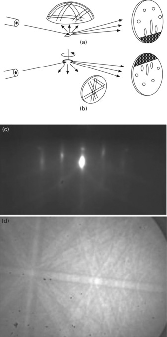
2.5 (a) The ‘astrodome’ geometry to allow simultaneous RHEED and Kikuchi pattern collection. (b) A dual screen geometry to allow RHEED and Kikuchi pattern collection during film growth. The simultaneous (c) RHEED pattern and (d) Kikuchi pattern of a SrTiO3 substrate at 650 °C and under a 1 × 10¹⁵ atoms/cm2 s flux of atomic oxygen using the dual screen geometry of (b) and a 30 keV RHEED beam energy. Reprinted with permission (Horio, 2006)
The particular location of Horio’s hemispherical screen does not allow for the use of this screen during film growth. Figure 2.5(b) shows a slightly altered geometry, with a second flat screen, that allows the Kikuchi screen to be monitored throughout the film growth processes – thereby providing in situ and real-time data collection. The electron beam has an angle of incidence on the sample of about 2°, as is standard for RHEED. The Kikuchi screen is 5 cm away from the sample with an angle of 45° to the sample normal. Figures 2.5(c) and (d) show simultaneous RHEED and Kikuchi images collected from a (001) SrTiO3 substrate after being heated to 650 °C under atomic oxygen. With this set-up, the strongest Kikuchi band contrast occurs with an incoming electron beam incident angle of around 15°. Zaefferer (2007) noted that maximum electron intensity is obtained when the angle of incidence of the electron beam and the angle of emission of the Kikuchi patterns are similar. This suggests that it would be advantageous to place a screen to capture the Kikuchi patterns with an angle to the sample normal of as close to 90° as possible, while still avoiding the main Bragg diffraction peaks. However, as will be discussed later, the best location for the screen depends on which particular sets of Kikuchi bands provide access to the most significant structural information.
One major concern with using the Kikuchi patterns for the structural analysis of thin films is the influence of diffraction from the substrate on the observed pattern. If the film is too thin, the electron beam will interact with the substrate as well as with the film. In general, 30 keV electrons have a penetration depth of roughly 500 Å. This is then decreased to about 50 Å because of the low angle of incidence of the electron beam to the sample. In agreement with this, C.J. Harland et al. (1981) determined an information depth of < 100 Å, while Kohl (1978) calculated an information depth of about 50–60 Å for the reciprocally related electron channeling patterns. This approximate probe depth of 50-100 Å is further experimentally supported by Baba-Kishi and Dingley (1989b) in work on bulk NiS2. These results imply that a film thickness of > 200 Å will be adequate to avoid the influence of the substrate on the Kikuchi pattern formation.
To gain qualitative information from the Kikuchi patterns requires two important pieces of geometrical information: the location of the pattern center – the point in the Kikuchi pattern that has no distortion from the gnomonic projection, and therefore relates back to the point source of electrons located within the sample – and the distance between the screen and the point source of electrons located within the sample. Three methods for obtaining this information are outlined in the literature: conic fitting (Biggin and Dingley, 1977; Venables and Binjaya, 1977), the circular mask technique (Venables and Binjaya, 1977), and the known orientation method (Baba-Kishi, 1998). Because epitaxial growth primarily occurs on a well- characterized single crystal substrate, ‘known orientation’ is the easiest and most accurate method.
In situ Kikuchi diffraction of epitaxial thin films allows several simplifications over the general procedure for analyzing the images. The first is that there is normally prior knowledge of the expected structure, so that a full ab-initio structure determination is not needed. The second is that the diffraction pattern of the substrate, when collected immediately prior to growth, can be directly compared with the as-grown film to determine changes in structure and to define the exact geometry. Finally, azimuthal rotation of the sample while collecting RHEED data also allows collection of a large portion of the Kikuchi pattern generated in the hemisphere above the sample, thus allowing many more zone axes to be seen. With the experimental geometry shown in Fig. 2.5(b), two-thirds of the hemisphere is visible, although owing to the flat nature of the phosphorus screen the edges of the images will be geometrically distorted.
Figure 2.6(a) shows a Kikuchi pattern, collected simultaneously with a RHEED image using the dual screen set-up of Fig. 2.5(b), of a SrRuO3 film grown on SrTiO3. This was collected right at the end of film growth while the substrate was still at 650 °C and exposed to an atomic oxygen flux of 1 × 10¹⁵ atoms/cm2 s. Figure 2.6(b) shows a simulated pattern of tetragonal SrRuO3, with various zone axes indexed, and exhibiting the same orientation as that of the experimental image.
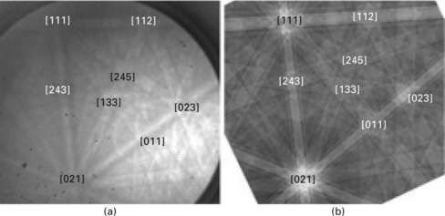
2.6 (a) The Kikuchi pattern of a SrRuO3 film grown on a SrTiO3 substrate at 650 °C and under a 1 × 10¹⁵ atoms/cm2 s flux of atomic oxygen; zone axes are indicated. (b) The calculated Kikuchi pattern for tetragonal SrRuO3 with the same orientation. Reprinted with permission (Ingle et al., 2010)
2.5 Lattice parameter determination
Lattice parameters can be determined from Kikuchi patterns by directly measuring the width and ratios of the low-order Kikuchi lines. To calculate a d-spacing, half the angle subtended by the Kikuchi bandwidth can be plugged into the Bragg equation. However, the band edge is not very sharp: in the order of 1 mrad, as compared with the 20 mrad Kikuchi band width for 30 keV electrons. This only allows an accuracy in the 3% range (Baba- Kishi and Dingley, 1989b; Dingley et al., 1995; Wilkinson, 1996) for lattice parameters.
The HOLZ rings found in many BKPs can also be used to help determine lattice parameters. Measuring the HOLZ ring diameter allows the d-spacing of the lattice planes perpendicular to the zone axis around which the ring is found to be calculated (Champness, 2001). This technique is more commonly used in CBED measurements. In general the HOLZ rings are sharper than the edges of Kikuchi bands; but they are not always present in BKPs, and even when they are the gnomonic projection needs to be properly accounted for. Michael and Eades (2000) used this technique and were able to obtain lattice parameter accuracies of better than 1% for many samples. However, they found that the largest error was in defining the radius of the HOLZ rings, and that error became quite large (up to 10%) for high atomic number samples.
2.6 Epitaxial film strain determination
Although determining lattice parameters from Kikuchi patterns is not very accurate, determining changes in lattice parameters, and hence strains, can be far more accurate. Troost et al. (1993) claim that by looking for changes in the angles between major zone axes, a strain sensitivity of about 0.1% is achievable. To study the elastic strain associated with epitaxial growth, the basic set-up used by Troost et al. (1993) on Si1-xGex epitaxial films grown on Si substrates involved etching away, ex situ, the epitaxial layer in one section of the sample. This allowed an SEM-based EBSD pattern to be collected from an unstrained standard, and from the film of interest, without any changes in the beam configuration geometry. The image from the unstrained standard could thus be directly compared with the image from the epitaxial film, allowing the determination of a change in angles between major zone axes. A straightforward method for doing this is to subtract the image of the unstrained substrate from that of the film (see Fig. 2.7). It is important to note that because this technique looks at the interzonal angles, it will be sensitive only to strains that distort the shape of the unit cell, and not to strains caused by hydrostatic expansion or contraction. With this procedure, Troost et al. (1993) found a marked reduction in the interzonal angle between the [100] and [111] zone axes of Si1-xGex, which provided evidence of a tetragonal elongation of 2.5% for x = 0.34 and at 1.0% for x = 0.16 along the [100] direction of the unit cell. High-resolution X-ray diffraction measurements support these conclusions.
2.7 (a) Circular subsection of a BKP from Si after contrast enhancement by background subtraction with superimposed indexing of the lattice planes. (b) Image resulting from the subtraction of a BKP of pure Si (100) from a BKP of an epitaxial Si0.66Ge0.34 layer indicating the tetragonal elongation between the [001] and [111] zone axes of the strained layer. Reprinted with permission (Troost et al., 1993).
A further enhancement of strain sensitivity, down to about 0.02%, was obtained by Wilkinson (1996) and Wilkinson et al. (2009), also on Si1-xGex epitaxial films grown on Si substrates. A similar etching procedure was used to provide a reference pattern for unstrained Si. Wilkinson (1996); Wilkinson et al. (2009) increased the sensitivity of the measurement primarily by increasing the sample-to-screen distance from 30 to 140 mm, thereby increasing the angular resolution of the detector. Using a more light-sensitive camera and computing the cross-correlation between multiple zone axes in both the strain-free reference images and the strained images further enhanced the ability to distinguish small changes in the location of the zone axes. In addition, the use of multiple zone axes allowed the full strain tensor and lattice rotations to be calculated.
The determination of elastic lattice strain in growing films requires an image of the substrate prior to growth, from which any change in the interzonal angles can be detected as the film is growing. Therefore, the ability of a dual screen RHEED and Kikuchi capture allows the in situ study of elastic strain as a function of film thickness and other growth parameters, in real time.
2.7 Kinematic and dynamic scattering
Kikuchi diffraction patterns are the result of multiple elastic and inelastic scattering processes, and thus present an inherently dynamic scattering problem. However, kinematic diffraction from a point source within the sample can account for the geometry of the patterns, and is straightforward to simulate. Obtaining patterns that can be easily compared with experimental images requires a fairly large number of lattice planes to be included. It is the dynamical scattering that leads to interference terms that produce the more complicated features, particularly when two or more Kikuchi lines intersect. Generally the manifestations of dynamical scattering are found on the low-order Kikuchi bands, which show intensity irregularities along the band edges and high contrast within the bands.
The dynamical models for electron diffraction start with the Bloch wave approach to describe the diffraction of electrons by the crystal lattice. The lattice provides a three-dimensional diffraction grating for the electrons that are incident on the sample. Depending on the incidence angle of an incoming plane wave relative to the lattice planes, the diffracted electrons interact differently with the atoms which constitute the crystal. This is the basic description of SEM-based ECPs (Reimer, 1985). A parallel beam of electrons interacts with the sample and produces a given intensity of electrons that are backscattered. As the angle of the incident beam of electrons is changed, the backscattered intensity changes, and a pattern is built up that looks very similar to a BKP. BKPs are, in fact, considered to be the reciprocal of ECPs (Reimer, 1985). The reciprocity means that the observed intensity at a point detector inside the sample, after diffraction of an incoming plane wave, is the same as for a detected plane wave intensity after diffraction of waves emanating from a point source inside the sample.
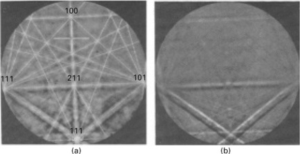
Winkelmann et al. (2007) created a three-step model of the dynamic scattering in BKP. The first step is the diffraction of a focused incident beam, which produces a distribution of electrons within the sample. This diffracted electron distribution is then subject to an inelastic process, which is accounted for in the model by quasi-elastic backscattering from atomic nuclei. The final step is the reciprocal of the ECP model, where the quasi-elastic backscattering generates point sources of electrons within the sample that are then subject to diffraction from the surrounding lattice. The cross-section for the quasi-elastic backscattering from the atomic nuclei and the probability of finding an electron at the atomic nuclei provide the source strength for the outgoing diffraction. In addition, the quasi-elastic backscattering also destroys the coherence between the incident beam diffraction and the outgoing beam diffraction. Wilkelman et al.’s application of the dynamical theory provided simulated patterns which very closely reproduced experimental BKPs of GaN, including HOLZ ring effects and zone axis fine structure, and provides a framework for more quantitative analysis of BKPs (see Fig. 2.8). Recent additional work by Winkelman (2010) suggests that the depth-distribution of backscattered electrons should also be taken into account in quantitative descriptions of Kikuchi pattern formation.
2.8 BKP of GaN 0001 at 20 kV: (a) experimental pattern; (b) dynamical simulation. In area B, attention is drawn to the HOLZ ring at approximately two-thirds of the radius of the area. The fine structure in areas A and C is strikingly similar in the two patterns. Reprinted with permission (Winkelmann, 2010).
Although dynamic scattering models for BKPs assume quasi-elastic scattering (Omoto et al., 2002; Winkelmann et al., 2007; Winkelmann, 2010), there is experimental evidence showing that electrons which lose up to 20% of the incident beam energy still participate in the formation of the Kikuchi pattern (Deal et al., 2008). Went et al. (2009) recently showed spectroscopic evidence that in BKPs there is an elastic peak that is separated from the loss distribution. They also found that electrons with less than 2.5 eV of energy loss, expected for the case of thermal diffuse scattering and still within the elastic peak, provide the most contrast. In essence, the experimental pattern should be considered as a sum of different patterns, each calculated for a specific energy loss, but strongly weighted towards quasi-elastic scattering.
As mentioned earlier, ECPs and BKPs are considered to be reciprocal measurements, and the general forms of the two patterns are indeed very similar. However, ECPs tend to show much more detail than the BKPs. This difference is a result of the much larger energy spread of electrons involved in the multi-step BKP pattern formation, as compared with the well-defined energy of the incident beam that generates the ECPs (Wilkinson and Hirsch, 1997).
As an alternative to a fully dynamic simulation, Zaefferer (2007) argues that the limited resolution of most cameras, and the different coherent scattering path lengths for all the electrons, lead to a blurring of the dynamical diffraction effects, resulting therefore in the appearance of bands of average intensities. Zaefferer showed that a significant improvement in the intensity calculations for BKPs over intensities that are proportional to the square of the structure factor, i.e. kinematic intensities, can be achieved by applying a relatively simple correction function to the kinematical intensities, originally proposed by Blackman (1939). This correction is appropriate only outside principal zone axes; nevertheless that accounts for a significant portion of the BKPs and therefore this approach may be a quick starting point for comparing experimental patterns to possible structures.
2.8 Epitaxial film structure determination
As discussed earlier, Wilkinson demonstrated that it is possible to obtain sensitivity to strains of approximately 0.02% on thick Si1–xGex epitaxial layers grown on planar Si substrates (Wilkinson, 1996). The method used – analysis of interzonal angles – is limited to strains that distort the shape of the unit cell. However, unit cell distortion is of primary interest in understanding the tetragonal distortion that can occur with epitaxial growth; therefore interzonal angles are one method for tracking epitaxially driven changes to the structure of thin films.
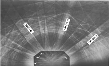
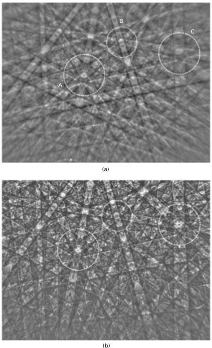
Another approach to exploring possible symmetry changes caused by epitaxy is highlighted by Baba-Kishi’s comparison of ZnS and CuFeS2 (Baba-Kishi, 1992, 2002). ZnS is cubic and CuFeS2 is tetragonal with a doubled ZnS-type structure. The symmetry features of BKPs in the cubic ZnS and those of the tetragonal CuFeS2 are very similar, since the tetragonal distortion in CuFeS2 is very small. However, it is possible to distinguish subtle changes to the BKP. The Kikuchi lines from CuFeS2 that intersect within the Kikuchi bands generated from the (024) plane highlight the slight tetragonal distortion. These Kikuchi line intersections are slightly offset from the center of the Kikuchi bands (see Fig. 2.9) and indicate that for CuFeS2 these planes are not mirror planes, as they would be for the cubic ZnS structure.
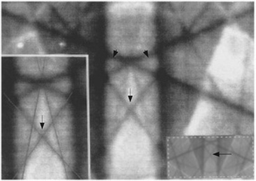
2.9 Kikuchi lines from CuFeS2 intersecting within the Kikuchi band formed from the (024) plane, showing a shift towards the right with respect to the large arrow which points to the center of the band. This shift at the intersection point originates from the tetragonal structure of CuFeS2. Inset: lines drawn over the Kikuchi lines to help indicate the asymmetry of the intersections with respect to the large black arrow. Reprinted with permission (Baba-Kishi, 2002).
Changes in the atomic positions within a unit cell may not be readily detected by these analysis techniques. Therefore it may also be of interest to look at the differences in the intensity of specific Kikuchi bands as a route to explore other epitaxially influenced changes in the structure of thin films. To sort out what to look for in the experimental Kikuchi pattern in order to help distinguish possible changes in the crystal structure of a film due to effects of epitaxy, a simulation is needed. If changes to the patterns can be found away from principal zone axes, then the corrected kinematic simulation scheme proposed by Zaefferer (2007) (and discussed above) may be an appropriate starting point.
An example of a possible epitaxial influence on the structure of a grown film is the potential buckling of the Cu–O planes in the high-pressure phase of SrCuO2 when grown with compressive strain. SrCuO2 is the end member (n = ∞) of the homologous high-pressure series Srn–1Cun+ 1O2n (Hiroi et al., 1991). Owing to the simplicity of the crystal structure and the planar nature of its Cu and O ordering, it is often called the parent compound of the high- temperature superconductors (Jorgensen et al., 1993) and is considered to be a two-dimensional quantum magnet (Yasuda et al., 2005). An extremely large change in the c-axis of this material was seen when it was grown by epitaxy with reduced a and b lattice parameters (Ingle et al., 2002). One possible explanation for this anomalous expansion in the c-axis is the buckling of the Cu–O planes, suggested by Vailionis et al. (1997). The proposed buckling of the Cu–O planes occurs by the motion of just the oxygen atoms, and as such it is extremely hard to see in x-ray diffraction. However, Kikuchi diffraction may be an ideal tool to look at the potential of an epitaxially driven change in the dimensionality of the Cu–O planes.
Figure 2.10 shows several changes in the Kikuchi pattern that are expected between planar and buckled Cu–O planes in SrCuO2, as simulated using the corrected kinematic scheme described by Zaefferer (2007). These Kikuchi patterns are centered around the (130) zone axis and indicate several possible changes in the pattern if the Cu–O planes were to buckle by the oxygen atoms moving in and out of the a–b plane by 10% of the c lattice constant (Fig. 2.10(b)) in contrast to a planar Cu–O structure (Fig. 2.10(a)). In this part of the Kikuchi pattern buckling causes an increase in intensity of the scattering from the {224} planes, indexed according to the enlarged unit cell required to describe buckling and highlighted in Fig. 2.10(b). Furthermore, there is also significant reduction in intensity expected for the (001) and (003) planes, as well as for the cubic-indexed {204} planes from the buckled structure (highlighted in Fig. 2.10(a)).
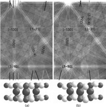
2.10 The calculated Kikuchi patterns, and structures, of the high- pressure phase of SrCuO2 without buckled Cu—O planes (a), and with buckled Cu—O planes (b). The light and dark lines at the top and bottom of the image are guides to the eye of the respective excess and deficient lines that define the edges of the Kikuchi bands that change between the two images. Reprinted with permission (Ingle et al., 2010).
There are a number of other expected changes in the Kikuchi pattern for the buckling of the Cu–O plane in SrCuO, but these are primarily in the high-index planes. While high-index planes are present in the image, they not only have an inherently lower intensity but they are also overlaid with the more intense low-index planes, and locations in the pattern are not always present that allow them to be seen. However, these simulations suggest that even subtle changes in the structure of epitaxially grown films might be quite distinguishable in an in situ and real-time dual-screen RHEED/ Kikuchi pattern collection set-up. In addition, the ability to collect a Kikuchi pattern from a well-characterized substrate just prior to the growth of a film provides a remarkable opportunity to minimize unknown experimental and geometrical effects in the patterns and to clarify the significant aspects of the simulations. This affords a tremendous advantage to the final analysis and interpretation of the Kikuchi patterns collected from an epitaxial film.
The use of more recent multi-beam dynamic models by Wilkelmann et al. (2007), which include improvements in the handling of inelastic scattering processes and the description of the excitation process, can provide much more detailed simulations. These models, along with continual improvements in hardware (Day, 2008) and software that are being applied to EBSD in SEMs, may allow a much more accurate and fine-grained approach to look for subtle changes in the atomic structure by inspecting and understanding the experimental Kikuchi patterns collected from thin epitaxial films.
2.9 Conclusion
The use of grazing incidence high-energy electrons during the growth of epitaxial films not only generates RHEED patterns from the elastically scattered electrons, but also generates Kikuchi patterns at larger scattering angles from the inelastically scattered electrons. These Kikuchi patterns can be analyzed to obtain an abundance of information about the crystallographic structure of the film. Of particular relevance to epitaxial film growth, the effects of strain and more generally the changes in space group and atomic positions of thin films can explored. These Kikuchi patterns can be collected in real-time, and simultaneously with the RHEED data with a dual-screen RHEED/Kikuchi collection set-up. The SEM-based EBSD community can provide a wealth of experience and has laid down a substantial amount of ground work that the film growth community can immediately use to help collect, analyze, and simulate Kikuchi patterns. In combination with standard RHEED analysis, the inelastically scattered electrons allow a remarkably complete set of data which help elucidate the full crystallographic structure of the potentially novel structures that can be formed by the influence of epitaxy on the growth of thin films.
2.10 References
Alam, M.N., Blackman, M., Pashley, D.W. High-angle Kikuchi patterns. Proceedings of the Royal Society of London, Series A. 1954; 221:224.
Baba-Kishi, K.Z. A study of directly recorded RHEED and BKD patterns in the SEM. Ultramicroscopy. 1990; 34(3):205–218.
Baba-Kishi, K.Z. Electron-microscopy of the mineral chalcopyrite, CuFeS2. Journal of Applied Crystallography. 1992; 25:737–743.
Baba-Kishi, K.Z. Measurement of crystal parameters on backscatter Kikuchi diffraction patterns. Scanning. 1998; 20(2):117–127.
Baba-Kishi, K.Z. Review – electron backscatter Kikuchi diffraction in the scanning electron microscope for crystallographic analysis. Journal of Materials Science. 2002; 37(9):1715–1746.
Baba-Kishi, K.Z., Dingley, D.J. Backscatter Kikuchi diffraction in the SEM for identification of crystallographic point groups. Scanning. 1989; 11(6):305–312.
Baba-Kishi, K.Z., Dingley, D.J. Application of backscatter Kikuchi diffraction in the scanning electron-microscope to the study of NiS2. Journal of Applied Crystallography. 1989; 22:189–200.
Biggin, S., Dingley, D.J. General method for locating X-ray source point in kossel diffraction. Journal of Applied Crystallography. 1977; 10(1):376–385.
Blackman, M. On the intensities of electron diffraction rings. Proceedings of the Royal Society of London Series A – Mathematical and Physical Sciences. 1939; 173(A952):0068–0082.
Boersch, H. About bands in electron diffraction. Physikalische Zeitschrift. 1937; 38:1000–1004.
Braun, W. Applied RHEED. Springer; 1999.
Braun, W., Daweritz, L., Ploog, K.H. Origin of electron diffraction oscillations during crystal growth. Physical Review Letters. 1998; 80(22):4935–4938.
Braun, W., Moller, H., Zhang, Y.H. Reflection high-energy electron diffraction during substrate rotation: a new dimension for in situ characterization. Journal of Vacuum Science & Technology B. 1998; 16(3):1507–1510.
Champness, P.E., Electron Diffraction in the Transmission Electron MicroscopeMicroscopy Handbook. BIOS Scientific Publishers Ltd, 2001. [Series no. 47.].
Cowley, J.M. Diffraction Physics. Netherlands: Elsevier Science BV; 1995.
Day, A.P. Spherical EBSD. Journal of Microscopy – Oxford. 2008; 230:472–486.
Deal, A., Hooghan, T., Eades, A. Energy-filtered electron backscatter diffraction. Ultramicroscopy. 2008; 108:116–125. [10.1016/j.ultramic.2007.03.010].
Dingley, D. Progressive steps in the development of electron backscatter diffraction and orientation imaging microscopy. Journal of Microscopy – Oxford. 2004; 213:214–224.
Dingley, D.J., Randle, V. Microtexture determination by electron back-scatter diffraction. Journal of Materials Science. 1992; 27(17):4545–4566.
Dingley, D.J., Wright, S.I. Determination of crystal phase from an electron backscatter diffraction pattern. Journal of Applied Crystallography. 2009; 42:234–241. [10.1107/S0021889809001654].
Dingley, D.J., Mackenzie, R., Baba-Kishi, K.Z. Applications of bkd for phase identification of crystals and strain measurement in materials. In: Russel P.E., ed. Microbeam Analysis, page 435. San Francisco PressInc, 1989.
Dingley, D.J., Baba-Kishi, K.Z., Randle, V. Atlas of Backscattering Kikuchi Diffraction Patterns. Bristol: Insitute of Physics; 1995.
Dobson, P.J. An introduction to reflection high energy electron diffraction. In: Howie A., Valdre U., eds. Surface and Interface Characterization by Electron Optical Methods. Plenum Press, 1988. [volume 191 of NATO ASI Series B, page 159,].
Field, D.P. Recent advances in the application of orientation imaging. Ultramicroscopy. 1997; 67:1.
Gajdardziska-Josifovska, M., Cowley, J.M. Brillouin zones and Kikuchi lines for crystals under electron channeling conditions. Acta Crystallographica Section a. 1991; 47:74–82.
Gareth, T. Transmission Electron Microscopy of Materials. Wiley; 1979.
Harland, C.J., Akhter, P., Venables, J.A. Accurate microcrystallography at high spatial-resolution using electron backscattering patterns in a field-emission gun scanning electron-microscope. Journal of Physics E-Scientific Instruments. 1981; 14(2):175–182.
Hiroi, Z., Azuma, M., Takano, M., Bando, Y. A new homologous series Srn–1Cun+ 1O2n found in the SrO-CuO system treated under high-pressure. Journal of Solid State Chemistry. 1991; 95(1):230.
Horio, Y. Kikuchi patterns observed by new astrodome RHEED. e-Journal of Surface Science and Nanotechnology. 2006; 4:118.
Horio, Y., Hashimoto, Y., Ichimiya, A. New type of RHEED apparatus equipped with an energy filter. Applied Surface Science. 1996; 100:292–296.
Ichimiya, A., Cohen, P.I. Reflection High Energy Electron Diffraction. Cambridge University Press; 2004.
Ingle, N.J.C., Hammond, R.H., Beasley, M.R. Molecular beam epitaxial growth of SrCuO2: Metastable structures and the role of epitaxy. Journal of Applied Physics. 2002; 91(10):6371–6378. [10.1063/1.1466876].
Ingle, N.J.C., Yuskauskas, A., Wicks, A., Paul, M., Leung, S. Topical review: the structural analysis possibilities of reflection high energy electron diffraction. Journal of Physics D – Applied Physics. 43, 2010. [133001,].
Jorgensen, J.D., Radaelli, P.G., Hinks, D.G., Wagner, J.L., Kikkawa, S., Er, G., Kanamaru, F. Structure of superconducting Sr0.9La0.1CuO2 (T = 42K) from neutron powder diffraction. Physical Review B. 1993; 47(21):14654.
Kikuchi, S. Diffraction of cathode rays by mica. Japanese Journal of Physics. 1928; 5:83.
Kohl, H.J.Sturgess J.M., ed. Proceedings of the 9th International Congress on Electron Microscopy (Toronto). 1978:198.
Lassen, N.C.K., Jensen, D.J., Conradsen, K. Image-processing procedures for analysis of electron back scattering patterns. Scanning Microscopy. 1992; 6(1):115–121.
Michael, J.R., Eades, J.A. Use of reciprocal lattice layer spacing in electron backscatter diffraction pattern analysis. Ultramicroscopy. 2000; 81(2):67–81.
Nakahara, H., Hishida, T., Ichimiya, A. Inelastic electron analysis in reflection high- energy electron diffraction condition. Applied Surface Science. 2003; 212:157–161. [10.1016/S0169-4332(03)00057-6].
Omoto, K., Tsuda, K., Tanaka, M. Simulations of Kikuchi patterns due to thermal diffuse scattering on MgO crystals. Journal of Electron Microscopy. 2002; 51(1):67–78.
Randle, V. Microtexture Determination and its Application. Bourne Press; 1992.
Reimer, L. Scanning Electron Microscopy. Springer-Verlag; 1985.
Schwarzer, R.A. Automated crystal lattice orientation mapping using a computer-controlled SEM. Micron. 1997; 28(3):249–265.
Small, J.A., Michael, J.R., Bright, D.S. Improving the quality of electron backscatter diffraction (EBSD) patterns from nanoparticles. Journal of Microscopy – Oxford. 2002; 206:170–178.
Staib, P., Tappe, W., Contour, J.P. Imaging energy analyzer for RHEED: energy filtered diffraction patterns and in situ electron energy loss spectroscopy. Journal of Crystal Growth. 1999; 201:45–49.
Troost, K.Z., Vandersluis, P., Gravesteijn, D.J. Microscale elastic-strain determination by backscatter Kikuchi diffraction in the scanning electron-microscope. Applied Physics Letters. 1993; 62(10):1110–1112.
Vailionis, A., Brazdeikis, A., Flodstrom, A.S. Observation of local oxygen displacements in CuO2 planes induced by a misfit strain in heteroepitaxially grown infinite-layer- structure Ca1–xSrxCuO2 films. Physical Review B. 1997; 55(10):6152.
Venables, J.A., Binjaya, R. Accurate micro-crystallography using electron backscattering patterns. Philosophical Magazine. 1977; 35(5):1317–1332.
Venables, J.A., Harland, C.J. Electron backscattering patterns – new technique for obtaining crystallographic information in scanning electron-microscope. Philosophical Magazine. 1973; 27(5):1193–1200.
Venables, J.A., Harland, C.J., Bin-Jaya. Developments in Electron Microscopy and Analysis. Academic Press, 1976; 101.
von Meibom, R., Rupp, E. Wide-angle electron diffraction. Zeitschrift für Physik. 1933; 82:690.
Wang, Z.L. Reflection Electron Microscopy and Spectroscopy for Surface Analysis. Cambridge University Press; 1996.
Wells, O.C. Comparison of different models for the generation of electron backscattering patterns in the scanning electron microscope. Scanning. 1999; 21(6):368–371.
Went, M.R., Winkelmann, A., Vos, M. Quantitative measurements of Kikuchi bands in diffraction patterns of backscattered electrons using an electrostatic analyzer. Ultramicroscopy. 2009; 109(10):1211–1216. [10.1016/j.ultramic.2009.05.004].
Wilkinson, A.J. Measurement of elastic strains and small lattice rotations using electron back scatter diffraction. Ultramicroscopy. 1996; 62(4):237–247.
Wilkinson, A.J., Hirsch, P.B. Electron diffraction based techniques in scanning electron microscopy of bulk materials. Micron. 1997; 28(4):279–308.
Wilkinson, A.J., Meaden, G., Dingley, D.J. Mapping strains at the nanoscale using electron back scatter diffraction. Superlattices and Microstructures. 2009; 45(4–5):285–294. [10.1016/j.spmi.2008.10.046].
Winkelmann, A. Principles of depth-resolved Kikuchi pattern simulation for electron backscatter diffraction. Journal of Microscopy – Oxford. 2010; 239(1):32–45. [10.1111/j.1365-2818.2009.03353.x].
Winkelmann, A., Trager-Cowan, C., Sweeney, F., Day, A.P., Parbrook, P. Many-beam dynamical simulation of electron backscatter diffraction patterns. Ultramicroscopy. 2007; 107(4-5):414. [DOI 10.1016/j.ultramic.2006.10.006].
Yasuda, C., Todo, S., Hukushima, K., Alet, F., Keller, M., Troyer, M., Takayama, H. Neel temperature of quasi-low-dimensional Heisenberg antiferromagnets. Physical Review Letters. 94(21), 2005. [217201, 3 217201.].
Zaefferer, S. On the formation mechanisms, spatial resolution and intensity of backscatter Kikuchi patterns. Ultramicroscopy. 2007; 107(2–3):254. [DOI 10.1016/j.ultramic.2006.08.007].