
CHAPTER 4
CMOS OPERATIONAL AMPLIFIERS
The CMOS operational amplifier is the most intricate, and in many ways the most important, building block of linear CMOS and switched-capacitor circuits. Its performance usually limits the high-frequency application and the dynamic range of the overall circuit. It usually requires most of the dc power used up by the device. Without a thorough understanding of the operation and the basic limitations of these amplifiers, the circuit designer cannot determine or even predict the actual response of the overall system. Hence this chapter includes a fairly detailed explanation of the usual configurations and performance limitations of operational amplifiers.
The technology, and hence the design techniques used for MOS amplifiers, change rapidly. Therefore, the main purpose of die discussion is to illustrate the most important principles underlying die specific circuits and design procedures. Nevertheless, the treatment is detailed enough to enable the reader to design high-performance CMOS operational amplifiers suitable for most linear CMOS circuit applications.
4.1. OPERATIONAL AMPLIFIERS [1, Chap. 10; 2, Chap. 6]
In switched-capacitor circuits—in fact, in all linear CMOS circuits—the most commonly used active component is the operational amplifier, usually simply called the op-amp. Ideally, the op-amp is a voltage-controlled voltage source (Fig. 4.1) with infinite voltage gain and with zero input admittance as well as zero output impedance. It is free of frequency and temperature dependence, distortion, and noise. Needless to say, practical op-amps can only approximate such an ideal device. The main differences between the ideal op-amp and the real device are the following [2, Chap. 6]:
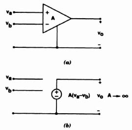
Figure 4.1. (a) Symbol for ideal op-amp; (b) equivalent circuit.
- Finite Gain. For practical op-amps, the voltage gain is finite. Typical values for low frequencies and small signals are A = 103 to 105, corresponding to 60 to 100 dB gain.
- Finite Linear Range. The linear relation νo = A(νa − νb) between the input and output voltages is valid only for a limited range of νa. Normally, the maximum value of νo for linear operation is somewhat smaller than the positive dc supply voltage; the minimum value of νa is somewhat positive with respect to the negative supply.
- Offset Voltage. For an ideal op-amp, if νa = νb (which is easily obtained by short-circuiting the input terminals), vo = 0. In real devices, this is not exactly true, and a voltage νo,off ≠ 0 will occur at the output for shorted inputs. Since νo,off is usually directly proportional to the gain, the effect can be more conveniently described in terms of the input offset voltage νin,off, defined as the differential input voltage needed to restore νo = 0 in the real device. For MOS op-amps, νin,off is typically ±2 to 10 mV. This effect can be modeled by a voltage source of value νin,off in series with one of the input leads of the op-amp.
- Common-Mode Rejection Ratio (CMRR). The common-mode input voltage is defined by
as contrasted with the differential-mode input voltage
Accordingly, we can define the differential gain AD (which is the same as the gain A discussed earlier), and also the common-mode gain AC, which can be measured as shown in Fig. 4.2, where AC = νo/νin,c. Here νin,off = 0 is assumed; |AC| is usually around 1 ≈ 10.

Figure 4.2. Op-amp with only common-mode input voltage.
The CMRR is now defined as AD/AC or (in logarithmic units) CMRR = 20 log10 (AD/AC) in decibels. Typical CMRR values for CMOS amplifiers are in the range 60 to 80 dB. The CMRR measures how much the op-amp can suppress noise, and hence a large CMRR is an important requirement.
- Frequency Response. Because of stray capacitances, finite carrier mobilities, and so on, the gain A decreases at high frequencies. It is usual to describe this effect in terms of the unity-gain bandwidth, that is, the frequency f0 at which |A(f0)| = 1. For CMOS op-amps, f0 is usually in the range 1 to 100 MHz. It can be measured with the op-amp connected in a voltage-follower configuration (Problem 4.13).
- Slew Rate. For a large input step voltage, some transistors in the op-amp may be driven out of their saturation regions or cut off completely. As a result, the output will follow the input at a slower finite rate. The maximum rate of change dνo/dt is called the slew rate. It is not directly related to the frequency response. For typical CMOS op-amps, slew rates of 1 to 20 V/μs can be obtained.
- Nonzero Output Resistance. For a real CMOS op-amp, the open-loop output impedance is nonzero. It is usually resistive and is on the order of 0.1 to 5 kΩ for op-amps with an output buffer; it can be much higher (≈ 1 MΩ) for op-amps with unbuffered output. This affects the speed with which the op-amp can charge a capacitor connected to its output, and hence the highest signal frequency.
- Noise. As explained in Section 2.7, the MOS transistor generates noise, which can be described in terms of an equivalent current source in parallel with the channel of the device. The noisy transistors in an op-amp give rise to a noise voltage νon at the output of the op-amp; this can again be modeled by an equivalent voltage source νn = νon/A at the op-amp input. Unfortunately, the magnitude of this noise is relatively high, especially in the low-frequency band, where the flicker noise of the input devices is high; it is about 10 times the noise occurring in an op-amp fabricated in bipolar technology. In a wide band (say, in the range 10 Hz to 1 MHz), the equivalent input noise source is usually on the order of 10 to 50 μV rms, in contrast to the 3 to 5 μV achievable for low-noise bipolar op-amps.
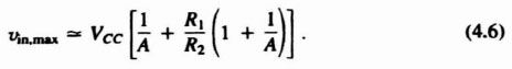
- Dynamic Range. Due to the limited linear range of the op-amp, there is a maximum input signal amplitude νin,max which the device can handle without generating an excessive amount of nonlinear distortion. If the power supply voltages of the op-amp are ±VCC. an optimistic estimate is νin,max ≈ VCC/A, where A is the open-loop gain of the op-amp. Due to spurious signals (noise, clock feedthrough, low-level distortion such as crossover distortion, etc.) there is also a minimum input signal νin,min which still does not drown in noise and distortion. Usually, νin,min is on the same order of magnitude as the equivalent input noise νn of the op-amp. The dynamic range of the op-amp is then defined as 20 log10(νin,max/νin,min) measured in decibels. When the op-amp is in open-loop condition, νin,max ≈ VCC/A, which is on the order of a millivolt, while
 , which is around 30 μV. Thus the open-loop dynamic range of the op-amp is only around 30 to 40 dB. However, the dynamic range of a circuit containing op-amps in negative feedback configuration can be much larger. As a simple illustration, consider the feedback amplifier shown in Fig. 4.3. It is easy to show (Problem 4.1) that the output due to the noise source νn acting alone has the rms value

Figure 4.3. Noisy feedback amplifier.
The voltage gain of the (noiseless) feedback circuit is
The minimum input signal νin,min gives rise to an output voltage approximately equal to νon. Hence
and for νo,max ≈ VCC,
Hence the dynamic range is given by
where the indicated approximation in usually valid for A
 1. For typical values (VCC ~ 5 V,
  , R2/R1 ≈ 5), a dynamic range of about 90 dB results for the overall circuit.
In linear CMOS circuits, dynamic range values around 80 to 90 dB are readily achievable. Even higher values (up to 100 dB) are possible if the large low-frequency noise (1/f noise) is canceled using a differential circuit configuration and chopper stabilization [3].
- Power Supply Rejection Ratio (PSRR). If a power supply voltage contains an incremental component ν due to noise, hum, and so on, a corresponding voltage Apν will appear at the op-amp output. The PSRR is defined as AD/Ap, where AD = A is the differential gain. It is common to express the PSRR in decibels; then PSRR = 20 log10(AD/Ap). Usual PSRR values range from 60 to 80 dB for the op-amp alone; for a switched-capacitor circuit, 30 to 50 dB can be achieved.
- DC Power Dissipation. Ideal op-amps require no dc power dissipated in the circuit; real ones do. Typical values for a CMOS op-amp range from 0.25 to 10 mW dc power drain.


To obtain near-ideal performance for a practical op-amp, the general structure of Fig. 4.4 is usually employed [1, Chap. 10]. The input differential amplifier (first block) is designed so that it provides a high input impedance, large CMRR and PSRR, low offset voltage, low noise, and high gain. Its output should preferably be single-ended, so that the rest of the op-amp need not contain symmetrical differential stages. Since the transistors in the input stage (and in subsequent stages) operate in their saturation regions, there is an appreciable dc voltage difference between the input and output signals of the input stage.
The second block in Fig. 4.4 may perform one or more of the following functions:
- Level Shifting. This is needed to compensate for the dc voltage change occurring in the input stage, and thus to assure the appropriate dc bias for the following stages.

- Added Gain. In most cases the gain provided by the input stage is not sufficient, and additional amplification is required.
- Differential-to-Single-Ended Conversion. In some circuits the input stage has a differential output, and the conversion to single-ended signals is performed in a subsequent stage.
The third block is the output buffer. It provides the low output impedance and larger output current needed to drive the load of the op-amp. It normally does not contribute to the voltage gain. If the op-amp is an internal component of a switched-capacitor circuit, the output load is a (usually small) capacitor, and the buffer need not provide a very large current or very low output impedance. However, if the op-amp is at the circuit output, it may have to drive a large capacitor and/or resistive load. This requires large current drive capability and very low output impedance, which can only be attained by using large output devices with appreciable dc bias currents. Thus the dc power drain will be much higher for such output op-amps than for interior ones.
As mentioned earlier, the ideal op-amp defined in Fig. 4.1 is a voltage-controlled voltage source, with zero output impedance. In fact, for practical op-amps, which do not have an output buffer, the output impedance may be very high, on the order of megohms. For such an amplifier, a better ideal representation can be found as a voltage-controlled current source, with a transconduction Gm value that is infinitely large. This ideal model is called an operational transconductance amplifier (OTA). If the op-amp has sufficiently high voltage gain and is in a stable feedback network, its output impedance is reduced to a very low value, and the difference between the performances of an op-amp and OTA can be neglected.
In a class of continuous-time filters, a finite-Gm transconductance is required. Here a low but accurately controlled value of Gm needs to be achieved. The corresponding active device is called a transconductor; it is not to be confused with an OTA. In the remainder of this chapter, the properties of typical CMOS op-amps and OTAs are described, and analysis and design techniques are given for them. Unless otherwise postulated, we assume that all devices are operated in the saturation region. Then iD is to a good approximation independent of νD and is given by iD ![]() k'(W/L)(νGS − VT)2. Here, due to body effect, VT depends on the source-to-body voltage.
k'(W/L)(νGS − VT)2. Here, due to body effect, VT depends on the source-to-body voltage.
4.2. SINGLE-STAGE OPERATIONAL AMPLIFIERS
A practical block diagram of an MOS op-amp was shown in Fig. 4.4 and is reproduced in more detail in Fig. 4.5. The voltage gain required is obtained in the differential (G1) and single-ended (G2) gain stages. The output stage (G3) is usually a wideband unity-gain low-output-impedance buffer, capable of driving large capacitive and/or resistive loads. If the op-amp is used in an internal (as opposed to output) stage of a switched-capacitor circuit, the load may be only a small capacitor, 2 pF or less. In such a situation, the output buffer (G3) may be omitted, and the load may then be connected directly to the output of G2. It will then function as an operational transconductance amplifier (OTA). In Fig. 4.5, if the combination of the differential stage and differential-to-single-ended converter provides adequate gain and output-voltage swing, G2 can also be omitted and the load may be driven directly by the differential stage. Again, the circuit will then realize an OTA.

Figure 4.5. Basic building blocks of an operational amplifier.
The CMOS differential stage with an active load is shown again in Fig. 4.6. It was introduced in Chapter 3. This stage combines the functions of a differential amplifier and differential-to-single-ended converter. The role of the differential amplifier is to amplify the difference between the two input voltages, ![]() and
and ![]() , regardless of the common-mode voltage. The differential stage is therefore characterized by its common-mode rejection ratio (CMRR), which is the ratio of the differential gain to the common-mode gain. The differential gain
, regardless of the common-mode voltage. The differential stage is therefore characterized by its common-mode rejection ratio (CMRR), which is the ratio of the differential gain to the common-mode gain. The differential gain ![]() was derived in Chapter 3 and is given by
was derived in Chapter 3 and is given by

In this equation, 1/(gd2 + gd4) is the output impedance seen at the output of the differential stage, and gmi is the transconductance of the input devices Q1 and Q2.

Figure 4.6. CMOS differential stage with active load.
The differential stage of Fig. 4.6 used as a single-stage op-amp has two major shortcomings. First, the total voltage gain is limited to the gain of a single-stage amplifier, which is typically about SO. Second, the output voltage swing is limited to the range
where νinc is the common-mode input voltage defined as ![]() , and VTP is the threshold voltage of the p-channel devices. Obviously, in most cases the low voltage gain and the narrow output swing prevent the differential stage of Fig. 4.6 from being useful as a single-stage op-amp.
, and VTP is the threshold voltage of the p-channel devices. Obviously, in most cases the low voltage gain and the narrow output swing prevent the differential stage of Fig. 4.6 from being useful as a single-stage op-amp.
The gain of the differential stage can be increased in two ways, by increasing the transconductance of the input devices Q1 and Q2, or by increasing the output impedance seen at the output of the stage. As can be seen from the relation gmi = ![]() , transconductance can be increased by increasing the width of the input devices and/or by increasing the bias current. Notice that reducing L, the channel length of the input devices, can also increase the transconductance. This, however, also has the opposite effect of reducing the output impedance 1/gdi of the input devices (due to channel-length modulation effect), and hence by Eq. (4.8) reduces the gain. Increasing the width or the current of the stage will increase the size or the power dissipation of the circuit. Therefore, a more efficient way to increase the gain is to increase the output impedance ro.
, transconductance can be increased by increasing the width of the input devices and/or by increasing the bias current. Notice that reducing L, the channel length of the input devices, can also increase the transconductance. This, however, also has the opposite effect of reducing the output impedance 1/gdi of the input devices (due to channel-length modulation effect), and hence by Eq. (4.8) reduces the gain. Increasing the width or the current of the stage will increase the size or the power dissipation of the circuit. Therefore, a more efficient way to increase the gain is to increase the output impedance ro.
As is evident from Fig. 4.6, to increase the output impedance ro both rd2 and rd4 have to be increased. This can be achieved by using the cascode current source as load. Figure 4.7 illustrates a differential stage that uses cascode transistors to increase the voltage gain by increasing the output impedance. Here devices Q1, Q1c and Q2, Q2c form two source-couple cascode amplifiers, while Q3, Q3c, Q4, and Q4c

Figure 4.7. CMOS differential stage with cascode load.
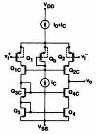
Figure 4.8. CMOS differential stage with cascode load and common-mode biasing scheme.
form a cascode current source that acts as an active load. For symmetrical dimensions (W/L)1 = (W/L)2, (W/L)3 = (W/L)4, (W/L)1c = (W/L)2c, and (W/L)3c = (W/L)4c the output impedance of the stage is,
where r1, || r2 denotes parallel-connected r1, and r2 (Problem 4.3). Since gm2crd2c and gm4crd4c are normally much greater than 1, ro ![]() (rd2 || rd4), which is the output impedance of the differential stage of Fig. 4.6. The differential voltage gain of the stage of Fig. 4.7 is given by
(rd2 || rd4), which is the output impedance of the differential stage of Fig. 4.6. The differential voltage gain of the stage of Fig. 4.7 is given by
The use of cascoding increases the gain of the differential stage substantially. The disadvantage is, however, that the voltage drops across the additional transistors Q1c and Q3c result in a reduction in the allowable input common-mode range and output voltage swing. The swing performance can be improved by using high-swing biasing of the cascode, as discussed in Section 3.3. The input common-mode range can also be improved, by using a bias voltage for Q1c and Q2c that tracks the input common-mode voltage. One circuit that accomplishes this is shown in Fig. 4.8, where Qb and Ic have been added to bias the gates of Q1c and Q2c. The W/L ratio of Qb and the value of current Ic can be selected in such a way that Q1 and Q2 remain biased at the edge of the saturation region as the input common-mode voltage changes. Obviously, the bias voltage Vbias will be one VGS drop (of Qb) below the voltage Vc of the common source. Even though the performance of the circuit of Fig. 4.8 improved over that of Figs. 4.6 and 4.7, due to the very limited output voltage swing the stage is normally not useful as a single-stage op-amp.

Figure 4.9. Folded-cascode op-amp consisting of a cascade of common-source and common-gate amplifiers.
Some of the problems described with the differential stage of Fig. 4.8 can be eliminated by using the folded-cascode configuration [4]. Consider the circuit of Fig. 4.8; let the bottom terminals (i.e., the sources of Q3 and Q4) of the composite load Q3, Q4 and Q1c to Q4c be disconnected from VSS, folded up, and connected to VDD instead. To assure proper dc bias currents, all NMOS devices must be replaced by PMOS types, and vice versa in the cascode loads; also, two additional current sources (Q5 and Q6) must be added between VSS and the drains of Q1 and Q2 to supply bias currents to these input devices. The resulting single-stage op-amp is shown in Fig. 4.9. The basic operation of the circuit is as follows. The dc current I0 of the current source Q7, is shared equally by Q1, and Q2. Also, the matched sources Q5 and Q6 draw equal bias currents ![]() from nodes A and B. Hence Q1c and Q2c also carry equal bias currents
from nodes A and B. Hence Q1c and Q2c also carry equal bias currents ![]() . A differential input voltage
. A differential input voltage ![]() and
and ![]() applied to the gates of Q1 and Q2 will offset their drain currents by ±ΔIo = ±gmi Δνin/2. Since the currents
applied to the gates of Q1 and Q2 will offset their drain currents by ±ΔIo = ±gmi Δνin/2. Since the currents ![]() of Q5 and Q6 remain unchanged, the currents of Q1c and Q2c (which are driven at their low-impedance source terminals) will also change by ±ΔIo. The current mirror Q3, Q4, Q3c, and Q4c transfers the current change in Q3 and Q3c to Q4 and Q4c. Hence the output voltage increment is gmiRoΔνin, where Ro is the output impedance at node D. It can be shown (Problem 4.4) that
of Q5 and Q6 remain unchanged, the currents of Q1c and Q2c (which are driven at their low-impedance source terminals) will also change by ±ΔIo. The current mirror Q3, Q4, Q3c, and Q4c transfers the current change in Q3 and Q3c to Q4 and Q4c. Hence the output voltage increment is gmiRoΔνin, where Ro is the output impedance at node D. It can be shown (Problem 4.4) that
The incremental gain is then
A disadvantage of the folded-cascode op-amp is the reduced output voltage swing due to the many (four) cascoded devices in the output branches. The swing can be increased if one of the bias circuits of Fig. 3.15 or 3.16 is used to establish the gate voltages of Q1c to Q4c such that the drain-to-source voltages of Q3 to Q6 are only slightly larger than VDsat. In Fig. 4.10 the bias circuits of Fig. 3.16 has been added to the op-amp. It can be shown (Problem 4.5) that the necessary aspect ratios are given by

Figure 4.10. Folded cascode op-amp with improved biasing for maximum output voltage swing.
For this circuit it can also be shown that the maximum output voltage swing is within the range
Thus the range lost at both the upper and lower limits is only 2|VDsat|. The cascode op-amp shown in Fig. 4.10 has a large voltage gain and a reasonably large output voltage swing. Hence it can be used as a single-stage OTA.
Consider next the high-frequency behavior of the circuit of Fig. 4.10. The poles of the gain stage are contributed by the stray capacitances loading nodes A, B, C, and D. The dominant pole sp1 of the circuit is due to the load capacitance CL in parallel with the output impedance Ro given by Eq. (4.12); hence its value is
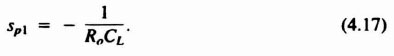

Figure 4.11. Small-signal low-frequency representation of the folded-cascode op-amp.
The resistance seen at node A is approximately 1/gm1c; at node B it is approximately 1/gm2c and at node C it is approximately 1/gm3. Since 1/gm is on the order of 1 kΩ and stray capacitances are much smaller then CL, the corresponding poles sp2, sp3, and sp4 are usually at much higher frequencies then sp1. The approximate low-frequency equivalent circuit is therefore that shown in Fig. 4.11. Here the input stage is represented by its simple Norton equivalent circuit, obtained using Eqs. (4.12) and (4.13). The overall transfer function is therefore

The frequency response is obtained by replacing s by jω.
4.3. TWO-STAGE OPERATIONAL AMPLIFIERS
The single-stage operational amplifier was discussed in Section 4.2. Another widely used CMOS op-amp uses the two-stage configuration based on the system of Fig. 4.5. This implementation is derived directly from its bipolar-transistor counterpart [5]. A simple two-stage CMOS implementation of the scheme of Fig. 4.5 is shown in Fig. 4.12, where the second gain stage, G2, drives a source follower. In this circuit Q6 acts as a simple current source, and devices Q1 to Q5 form a differential stage (cf. Fig. 4.6) with a single-ended output. Transistors Q6 (acting as the driver device) and Q7 (acting as the load) form the second gain stage, which also acts as a level shifter. Finally, the source follower consisting of Q8 as driver and Q9 as load realizes the output buffer. The low-frequency differential-mode gain of the input stage can be obtained from Eq. (4.8):
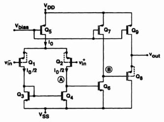
Figure 4.12. Uncompensated two-stage CMOS operational amplifier.

where the subscript i refers to input, and l to load device.
Here it is assumed that Q1 is matched to Q2, and Q3 to Q4. The low-frequency gain of the inverter formed by Q6 and Q7 is clearly

The overall voltage gain Aν is Aν1Aν2. For typical biasing conditions and device geometries, Aν = 10,000 to 20,000 can be achieved. The output terminals A and B of both stages are high-impedance nodes; the low-frequency output impedance of the input stage driving node A is
that of the second stage (Q6, Q7) is

An equivalent circuit showing these impedances and also the parasitic capacitances CA and CB loading nodes A and B, respectively, is shown in Fig. 4.13. It is evident from the figure that the transfer function of the amplifier Aν(s) = Vout(s)/![]() will contain the factors
will contain the factors
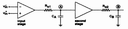
Figure 4.13. Block diagram showing the origin of the dominant poles.

where the poles are sA = −1/Ro1CA and sB = −1/Ro2CB. Since Ro1 and Ro2 are large, sA and sB will be close to the jω axis in the s plane. Hence they will be the dominant poles of the amplifier. The effects of other poles will be noticeable only at very high frequencies.
If the op-amp is required to drive small internal capacitive leads only, the output source follower (Q8, Q9) may be eliminated and the output taken directly from node B. However, even for such capacitive loads, the maximum output current that can be sourced is limited by the current source Q7.
For very high gain applications, the cascode differential amplifier of Fig. 4.8 can be used as the first stage of the op-amp. A two-stage op-amp with the cascode differential stage is shown in Fig. 4.14. Transistors Q8 and Q9 form a level shifter between the output of the first stage and the input of the second stage, to balance the dc level between the signal path. The gain of the first stage is given by Eq. (4.11), and the total gain is
where Ro1 is given by Eq. (4.10). The frequency response given by Eq. (4.23) is still valid, with sA = −1/Ro1CA, where Ro1 is replaced by its new value given by Eq. (4.10).
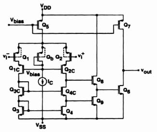
Figure 4.14. Two-stage op-amp with cascade differential stage.
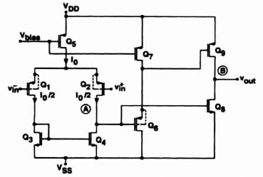
Figure 4.15. Improved uncompensated CMOS operational amplifier.
An improved CMOS op-amp [6] with increased output range and current drive capability is shown in Fig. 4.15. The output stage consists of devices Q6 to Q9, with Q6 and Q7 acting as a level shifter and Q8 and Q9 acting as a class B push-pull output stage. The dc biasing is designed so that Q8 and Q9 have equal-valued small gate-to-source dc biases. This maximizes the linear νout range. The conceptual form of the CMOS gain stage with the level shifter is shown in Fig. 4.16.
The low-frequency small-signal gain of the second stage can be found from the equivalent circuit of Fig. 4.17. The node equation is
so that
Since gm can be 100 times larger than gd, the gain is high. The low-frequency small-signal differential gain can easily be found from Eqs. (4.19) and (4.26):
Thus |Aν| can be as high as 20,000. However, if the circuit has to drive a resistive load GL, then gd8 + gd9 is replaced by gd8 + gd9 + GL, which normally reduces the gain significantly. Also, for a large load capacitance CL, the pole of the compensated op-amp in a feedback arrangement resulting from the time constant CL/(gd8 + gd9) may move so close to the jω axis that instability occurs. Hence this op-amp is again suited only for driving small-to-moderate-sized internal capacitive loads.

Figure 4.16. CMOS gain stage with level shifter.
If the circuit of Fig. 4.15 is to be used to drive resistive loads, an output buffer stage must be added. This may be simply a source follower, similar to that in Fig. 3.33. However, better output current sourcing and sinking, and lower output impedance, can be obtained using more elaborate CMOS output buffers. These are discussed in Section 4.9.
Consider now the high-frequency behavior of the circuit of Fig. 4.15. As before, nodes A and B are at a high impedance level and are responsible for the dominant poles. The approximate equivalent circuit is shown in Fig. 4.18. Here, the input stage is represented by a simple Norton equivalent, obtained using Eqs. (4.19) and (4.21). Similarly, the Norton equivalent of the output stage can be found from Eqs. (4.26) and (4.22). As before, the transfer function contains a factor similar to that given in Eq. (4.23), where now sA = −(gd + gd4)/CA and sB = −(gd8 + gd9)/CL. The overall transfer function is therefore

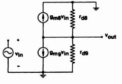
Figure 4.17. Small-signal equivalent circuit of the CMOS gain stage.
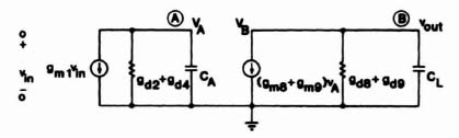
Figure 4.18. Two-stage representation of the CMOS operational amplifier of Fig. 4.15.
The frequency response is obtained by replacing s by jω. For low frequencies (ω ![]() |sA|, |sB|),
|sA|, |sB|),
For high frequencies (to ![]() |sA|, |sB|),
|sA|, |sB|),

Hence, for high frequencies, the amplifier inverts the input voltage. In switched-capacitor applications the op-amp always has a feedback capacitor C connected between its output and its inverting input terminals. A typical circuit is shown in Fig. 4.19. A sine-wave signal Vin, (jω) appearing at the inverting input terminal will thus be amplified by −Aν(jω) and fed back to the input via capacitive divider C and C1; here C1 represents the overall capacitance of the input circuit driving the op-amp, including stray capacitances, and so on.
The op-amp and capacitor C and C1 form a feedback loop, with a loop gain

Figure 4.19. Operational amplifier with feedback capacitor C and input capacitor Cin.
In addition to the input voltage νin, the circuit also contains the voltage νn, representing the noise generated in (or coupled to) the op-amp. The circuit can be analyzed by using the node equation at node A:
and the op-amp gain relation:
This gives

The output voltage can become (in theory) infinite if the input signal or noise contains a sine-wave component with a frequency to ω1, such that
By Eq. (4.31) this corresponds to a loop gain of AL = 1, a condition for oscillation.
At dc and very low frequencies Eq. (4.29) shows that Aν(jω) is positive, and hence Eq. (4.35) cannot be valid. However, at high frequencies, by Eq. (4.30), Aν(jω) becomes negative real, and at some ω1 it may satisfy Eq. (4.35). When this occurs, the circuit will become unstable, and it will oscillate with a frequency ω1. In theory, for our two-pole model, Aν(jω) becomes negative real only for to ω → ∞; however, for large loop gain the circuit is only marginally stable for high frequencies, so that any additional small phase shift due to the high-frequency poles neglected in Fig. 4.18 may cause oscillation. Even if stability is retained, the transient response contains a lightly damped oscillation, which is unacceptable in most applications.
To prevent oscillation in feedback amplifiers, and to ensure a good transient response, an additional design step (called frequency compensation) is needed. It is based on the stability theory of feedback systems and is discussed briefly in the next section.
4.4. STABILITY AND COMPENSATION OF CMOS AMPLIFIERS
In Section 4.3 it was shown that the CMOS op-amp of Fig. 4.15 is only marginally stable when used in a feedback circuit. In this section the analysis of stability and the design steps required to ensure stable feedback op-amps are discussed.
A systematic investigation of stability can be based on the general block diagram of Fig. 4.20, which shows an op-amp in a negative feedback configuration. It is assumed that k and a are positive constants, and k ≤ 1. The voltage at the inverting input terminal is
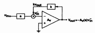
Figure 4.20. Operational amplifier with negative feedback.
and the output voltage is
Hence the voltage gain is

Aνf is often called the closed-loop gain, Aν is the open-loop gain of the system; and kAν is the loop gain.
We assume next that all poles si, of Aν(s) are due to stray capacitances to ground in an otherwise resistive circuit. (This is an acceptable approximation if inductive effects are negligible, and all capacitances loading the high-impedance nodes are connected between voltages that are in phase or 180° out of phase of each other.) Then all si are negative real numbers, and Aν(s) is in the form
For s = jω, Aν(jω) gives the frequency response of the op-amp. Its magnitude is

and its phase is given by

Note that both |Aν(jω)| and ![]() Aν(jω) are monotone-decreasing functions of ω.
Aν(jω) are monotone-decreasing functions of ω.
The natural frequencies of the overall feedback system are the poles sp of Aν(s), which by Eq. (4.38) satisfy the relation

For stability, all sp must be in the negative half of the s plane; that is, the real parts of all poles must be negative. Now assume that Re[kAν(jω)] > − 1 for all real values of ω. Then kAν(jω) ≠ − 1, and hence no sp can occur on the jω axis; furthermore, it can easily be proven that if Aν(s) has only poles with negative real parts, then under the stated assumption, so will Aνf(s). The proof is implied in Problem 4.26. Thus the condition
is sufficient to ensure stability. It is not, however, a necessary condition. Two other sufficient conditions for stability can also readily be stated. Let ω180 go be the frequency at which the monotone decreasing phase of kAν(jω) reaches − 180°; that is,
If now |kAν(jω180| < 1, Eq. (4.42) cannot hold on the jω axis, and hence the circuit is stable. A measure of its stability is the gain margin, defined as
The gain margin must be negative for stability; the more negative it is, the larger the margin of stability of the circuit. Normally, a margin of at least 20 dB is desirable.*
Next, let |kAν(jω180)|, which also decreases monotonically with ω, reach the value 1 (i.e., 0 dB) at the unit-gain frequency ω0. Then, if the phase at ω0 satisfies ![]() kAν(jω0) > − 180°, the system will be stable. The phase margin PM, defined as
kAν(jω0) > − 180°, the system will be stable. The phase margin PM, defined as ![]() kAν(jω0) + 180°, is a measure of its stability; the larger the phase margin, the more stable the circuit. Usually, at least a 60° (and preferably larger) margin is required. This will also give a desirable (i.e., nonringing) step response for the closed-loop amplifier. The overshoot, OS, of the step response of the feedback system decreases rapidly with increasing phase margin: for PM = 60°, OS = 8.7%; for PM = 70°, OS = 1.4%, and for PM = 75°, OS = 0.008%.
kAν(jω0) + 180°, is a measure of its stability; the larger the phase margin, the more stable the circuit. Usually, at least a 60° (and preferably larger) margin is required. This will also give a desirable (i.e., nonringing) step response for the closed-loop amplifier. The overshoot, OS, of the step response of the feedback system decreases rapidly with increasing phase margin: for PM = 60°, OS = 8.7%; for PM = 70°, OS = 1.4%, and for PM = 75°, OS = 0.008%.
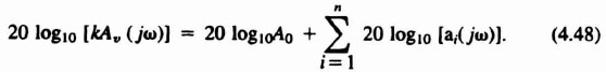
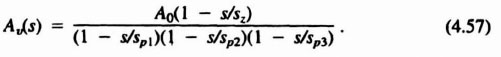
All the stability conditions above can readily be visualized and checked using Bode plots. These show |kAν(jω)| (in decibels) and ![]() kAν(jω) (in degrees) as functions of ω on a logarithmic scale. Typical plots are shown in Fig. 4.21 (dashed curves) for the three-pole loop gain:
kAν(jω) (in degrees) as functions of ω on a logarithmic scale. Typical plots are shown in Fig. 4.21 (dashed curves) for the three-pole loop gain:

Figure 4.21. Bode plot for three real poles.

with A0 = 105, s1 = −10 rad/s, s2 = −103 rad/s, and s3 = −103 rad/s. Drawing the magnitude plot is simplified by using an asymptotic approximation to the logarithmic magnitude of the general term ai(jω) = 1/(1 − jω/s1):

Clearly, 20 log10|ai| ≈ 0 for |ω| ![]() |si| and 20 log10|ai| ≈ −20(log10ω − log10|si|) for |ω|
|si| and 20 log10|ai| ≈ −20(log10ω − log10|si|) for |ω| ![]() |si|. Figure 4.22 illustrates the approximation of |ai| and also the phase
|si|. Figure 4.22 illustrates the approximation of |ai| and also the phase ![]() ai(jω) of ai(jω). An important conclusion which can be drawn from the figure is that for |ω|
ai(jω) of ai(jω). An important conclusion which can be drawn from the figure is that for |ω| ![]() |si|, 20 log10|ai| approaches a straight line with a slope of − 6 dB/octave (i.e., decreases by 6 dB for each doubling of ω). while
|si|, 20 log10|ai| approaches a straight line with a slope of − 6 dB/octave (i.e., decreases by 6 dB for each doubling of ω). while ![]() ai approaches − 90° in this same region. In particular, |
ai approaches − 90° in this same region. In particular, |![]() ai| ≈ 90° for ω > 5|si|. Also, |
ai| ≈ 90° for ω > 5|si|. Also, |![]() ai| ≤ 30° for ω < 0.5|si|; this fact will be used later.
ai| ≤ 30° for ω < 0.5|si|; this fact will be used later.

Figure 4.22. Gain and phase responses for a factor ai(jω) = (1 − jω/si)−1.
The logarithmic form of the loop gain satisfies
Therefore, at the unity-gain frequency ω0 the slope of the logarithmic loop gain versus logarithmic frequency is approximately −6m dB/octave, while its angle is around −90m degrees. Here, m is the number of those poles whose magnitude |si| is less than ω0. Clearly, for a substantial positive phase margin (say 60°, so that ![]() kAν(jω0) > 120°), m should be less than 2. Ideally, m is 1 (i.e., there is only one pole satisfying |si| < ω0), and the other poles have much larger magnitudes than ω0. Then the phase margin is close to 90°. (For A0
kAν(jω0) > 120°), m should be less than 2. Ideally, m is 1 (i.e., there is only one pole satisfying |si| < ω0), and the other poles have much larger magnitudes than ω0. Then the phase margin is close to 90°. (For A0 ![]() 1, m = 0 is impossible.)
1, m = 0 is impossible.)
Returning to the example of Fig. 4.21, the solid lines show the asymptotic approximation to the logarithmic magnitude of kAν(jω). The curves indicate that at the unity-gain frequency ω0 ≈ 4 krad/s, the phase of kAν(jω) is about −270°. Hence the phase margin is negative, and the feedback system is potentially unstable.
The modification of kAν(s), which changes an unstable feedback system into a stable system, is called frequency compensation. Its purpose is usually to achieve the ideal situation described above; thus we aim to realize a loop gain that contains exactly one pole smaller in magnitude than ω0, while all others are much larger. Since the feedback factor k can be anywhere in the 0 < k ≤ 1 range, and k = 1 represents the worst case (i.e., the largest ω0 and hence the smallest phase margin), this will be assumed from here on. Note that k ![]() 1 corresponds to C
1 corresponds to C ![]() Cin in Fig. 4.19 and k = 1 represents a short circuit between the output and the inverting input of the amplifier. Such a circuit is shown in Fig. 4.77 in connection with Problem 4.13.
Cin in Fig. 4.19 and k = 1 represents a short circuit between the output and the inverting input of the amplifier. Such a circuit is shown in Fig. 4.77 in connection with Problem 4.13.
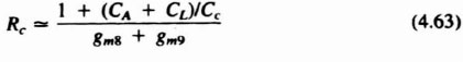
It will next be shown how to carry out the compensation for the op-amp of Fig. 4.15. Referring to its equivalent small-signal representation (Fig. 4.18), we will first attempt to achieve compensation by connecting a compensating capacitor Cc between the high-impedance nodes A and B, as shown in Fig. 4.23. It is well known (see Ref. 2, Sec. 9.4) that for bipolar op-amps the addition of such capacitor moves the pole associated with node A to a much lower frequency, while that corresponding to node B becomes much larger. It is therefore often called a pole-splitting capacitor and (for bipolar op-amps) accomplishes the desired compensation. The situation is less favorable for MOS op-amps, as will be shown next. The node equations for nodes A and B in Fig. 4.23 are
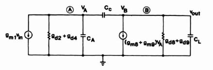
Figure 4.23. Two-stage representation of a CMOS operational amplifier with a pole-splitting capacitor Cc.
and
Solving for Vout, the voltage gain
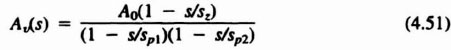
results. Hence the dc gain is
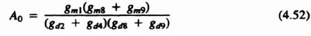
and the zero is
The calculation of the poles is simplified if it is a priori assumed that |sp2| ![]() |sp2 and that gm8 + gm9
|sp2 and that gm8 + gm9 ![]() gd2 + gd4 or gd8 + gd9. Then, after some calculation [2, p. 519] (see Problem 4.6),
gd2 + gd4 or gd8 + gd9. Then, after some calculation [2, p. 519] (see Problem 4.6),


where A0 is the dc gain given in (4.52).
Physically, Cc (multiplied by the Miller effect) is added in parallel to CA, thus reducing |sp| by a very large (ca. 103) factor, while at the same time it increases the second pole frequency |sp1| via shunt feedback.
Clearly, |sp1| decreases, while |sp2| increases with increasing values of Cc. Thus Cc indeed splits the poles apart, as originally intended. Unfortunately, the desired compensation is nevertheless usually not achieved, due to the positive (right-half-plane) zero sz. For the usual case of 1/Cc ![]() 1/CA + 1/CL, the inequalities
1/CA + 1/CL, the inequalities
hold. The logarithmic magnitude of the factor (1 − jω/sz) is near zero for |ω| ![]() sz, while it increases by about 6 dB/octave for |ω|
sz, while it increases by about 6 dB/octave for |ω| ![]() sz. The phase of the factor is −tan−1 (ω/sz); it decreases from 0 to −90° as ω grows from zero to infinity. As a result, the plots shown in Fig. 4.24 are obtained. Clearly, at the unity-gain frequency too the phase is less than −180°. Hence in a feedback configuration the amplifier can become unstable. Note that if gm8 + gm9 would be increased, sz|sp1|A0 would, by Eqs. (4.52) to (4.54), increase proportionally. It is clear from Fig. 4.24 that if sz/|sp1 (in octaves) is greater than A0 (in dB)/6, the unity-gain frequency ω0 is less than sz, and the phase margin is positive. Thus, for sufficiently high gm values (such as are afforded by bipolar transistors), the inclusion of Cc accomplishes the desired stabilization. Unfortunately, the transconductance of MOSFETs is normally not high enough for the purpose, and other arrangements must be found to eliminate sz.
sz. The phase of the factor is −tan−1 (ω/sz); it decreases from 0 to −90° as ω grows from zero to infinity. As a result, the plots shown in Fig. 4.24 are obtained. Clearly, at the unity-gain frequency too the phase is less than −180°. Hence in a feedback configuration the amplifier can become unstable. Note that if gm8 + gm9 would be increased, sz|sp1|A0 would, by Eqs. (4.52) to (4.54), increase proportionally. It is clear from Fig. 4.24 that if sz/|sp1 (in octaves) is greater than A0 (in dB)/6, the unity-gain frequency ω0 is less than sz, and the phase margin is positive. Thus, for sufficiently high gm values (such as are afforded by bipolar transistors), the inclusion of Cc accomplishes the desired stabilization. Unfortunately, the transconductance of MOSFETs is normally not high enough for the purpose, and other arrangements must be found to eliminate sz.

Figure 4.24. Amplitude and phase plots of the CMOS op-amp.
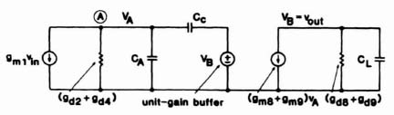
Figure 4.25. Unity-gain buffer ammgement used to eliminate the right-plane zero.
One scheme for getting rid of sz is to shift it to infinite frequency. Physically, the zero is due to the existence of two paths through which the signal can propagate from node A to node B. The first is through Cc, while the second is by way of the controlled source (gm8 + gm9)νA. For s = sz the two signals from these paths cancel, and a transmission zero occurs. The zero can be shifted to infinite frequency by eliminating the feedforward path through Cc, at the cost of an extra unity-gain buffer (Fig. 4.25). A detailed analysis shows (Problem 4.7) that the numerator of Aν(s) is now simply A0, while the denominator remains nearly the same as in Eq. (4.51). A circuit implementing this scheme is shown in Fig. 4.26, where Q10/Q11 form the buffer.

Figure 4.26. Internally compensated CMOS op-amp with unity-gain buffer used to avoid the right-half-plane zero.
An alternative (and simpler) scheme [7] can also be used. Consider the circuit shown in Fig. 2.27. Nodal analysis shows (Problem 4.8) that its transfer function is
Here A0, sp1, and sp2 are (as before) given by Eqs. (4.52), (4.54), and (4.55), while now


As Eq. (4.58) shows, it is again possible for this circuit to shift sz to infinity, if Rc = 1/(gm8 + gm9) is chosen. Then, choosing a sufficiently large value for Cc can split the poles. To quantify this, it is reasonable to require that |sp2| > ω0, the unity-gain frequency. For this choice, since in the frequency region between |sp1| and |sp2|

holds, the approximation ω0 ≈ A0 |sp1| can be used. Thus |sp2| > A0|sp1| may be specified. From Eq. (4.55), with 1/Cc ![]() (1/Cc + 1/CL), we require
(1/Cc + 1/CL), we require

so that a feedback capacitor satisfying
is needed. Since experience indicates that normally Cc ~ CL is a good choice, we require that gm1 < gm8 + gm9. Another way of eliminating sz for the circuit of Fig. 4.27 is by pole-zero cancellation. Choosing sz = sp2, from Eqs. (4.55) and (4.58),
is obtained. The resulting cancellation leaves the op-amp with a two-pole response.
Figure 4.27. Small-signal equivalent circuit of CMOS op-amp with nulling resistor for compensation.
Compensation now requires that |sp3| > |A0|sp1|. Using Eqs. (4.55), (4.59), and (4.61), this condition can be rewritten in the form
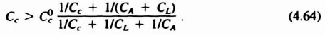
Here ![]() is the bound given for Cc on the right-hand side of Eq. (4.62). The factor multiplying
is the bound given for Cc on the right-hand side of Eq. (4.62). The factor multiplying ![]() in Eq. (4.64) is usually much smaller than 1; hence, now a smaller Cc can be used. Its value can be obtained from the bound*
in Eq. (4.64) is usually much smaller than 1; hence, now a smaller Cc can be used. Its value can be obtained from the bound*

The actual implementation of the scheme of Fig. 4.27 in the CMOS op-amp of Fig. 4.15 is shown in Fig. 4.28. The parallel-connected channels of the complementary transistors Q10 and Q11 form Rc. This push-pull arrangement helps to suppress even harmonics and thus improves the linearity of the resistor Rc.
Note that the condition Rc = 1/(gm8 + gm9) is easily obtained by matching Q10 and Q11 to Q9 and Q10, respectively. Satisfying Eq. (4.63) is somewhat harder; however, the accuracy is not critical, and as explained above, this choice for Rc results in a smaller value for Cc.
The pole-splitting frequency compensation technique described so far is applicable to a two-stage topology where the output stage is a common-source gain stage preceded by a differential stage preamplifier. If the op-amp is loaded with a very small resistance, the gain of the output stage can become so small that the two-stage solution may not have enough dc gain. In this case, using the cascode load differential amplifier shown in Fig. 4.7 can increase the gain of the two-stage amplifier. Alternatively, the folded-cascode topology of Fig. 4.10 can also be used as the input stage in which case the op-amp can be frequency stabilized with a pole-splitting capacitor that is connected between the two high-impedance nodes. Another method to enhance the op-amp gain is to use a multistage configuration. The simplest approach would be to insert a positive gain intermediate stage between the input and output stages. This is shown in simplified form in Fig. 4.29. The three-stage amplifier has three dominant poles, one at the output of each gain stage. The simple pole splitting does not remove the third pole, and to stabilize such a topology a nested Miller [8] compensation must be used. This compensation technique uses the two capacitors Cc1 and Cc2 shown in Fig. 4.29. Cc1 is connected between the final output and the output of the intermediate stage. Cc2 is connected between the final output and the output of the differential stage. Figure 4.30 shows the three-stage op-amp of Fig. 4.29 in more detail. It consists of a p-channel input differential pair Q1–Q4 followed by the differential pair Q5–Q8, that serves as the positive gain intermediate stage. The output stage is a common-source amplifier made of transistors Q9 and Q10. The op-amp is stabilized by capacitors Cc1 and Cc2. The small-signal equivalent circuit of the three-stage amplifier using the nested Miller compensation scheme is shown in Fig. 4.31 [8].
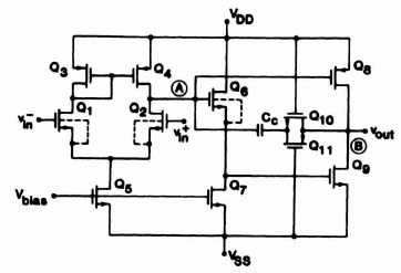
Figure 4.28. Improved internally compensated CMOS operational amplifier.
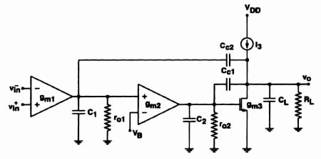
Figure 4.29. Nested Miller compensation scheme for a three-stage op-amp.
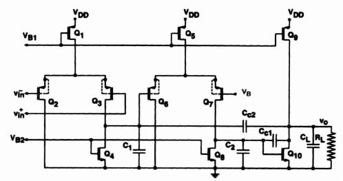
Figure 4.30. Simplified circuit diagram of a three-stage op-amp with nested Miner compensation.
The open-loop gain of the uncompensated op-amp has three dominant poles sp1, sp2, and sp3. The location of the three poles are given by


where Req = ro3||RL is the equivalent output impedance of the third stage.
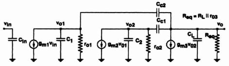
Figure 4.31. Small-signal equivalent circuit of the three-stage op-amp.
The transfer function of the uncompensated op-amp is
where A0 is the dc open-loop gain given by
The magnitude plot of the combined intermediate- and output-stage gain is shown in Fig. 4.32a, where f2 = 1/(2πro2C2) and f3 = 1/(2πReqCL) are the pole frequencies. The combination of the intermediate and output stages is compensated by the first Miller capacitor Cc1. The insertion of this capacitor splits the poles such that f3 is shifted to a higher frequency, ![]() and f2 to a lower frequency,
and f2 to a lower frequency, ![]() . The new location of the poles is given by
. The new location of the poles is given by
It is worth noting that the insertion of Cc1 splits sp2 and sp3 to the same location, as was the case with the poles of the two-stage op-amp described earlier in this chapter. Also, the location of the pole sp1, corresponding to the input stage, remains unaltered.
The frequency characteristic of the complete three-stage op-amp is shown in Fig. 4.32b where the third pole sp1 corresponding to the input stage has been added. The result of inserting the first compensation capacitor Cc1 is a frequency response that contains the two dominant poles sp1 and ![]() . These two poles can be split by inserting the second compensation capacitor Cc2, which shifts f1 to a higher frequency,
. These two poles can be split by inserting the second compensation capacitor Cc2, which shifts f1 to a higher frequency, ![]() , and
, and ![]() to a lower frequency,
to a lower frequency, ![]() (dominant pole). The result is an op-amp with an open-loop response with one dominant pole at
(dominant pole). The result is an op-amp with an open-loop response with one dominant pole at ![]() and a magnitude response that has a straight 6-dB/octave roll-off from the dominant pole frequency
and a magnitude response that has a straight 6-dB/octave roll-off from the dominant pole frequency ![]() up to the unity-gain frequency.
up to the unity-gain frequency.
Inserting the two nested Miller compensation capacitors Cc1 and Cc2, as in the case of the two-stage op-amp, introduces right-half-plane zeros. Similar strategies described earlier in this section, such as the zero blocking technique or placing a resistor in series with the Miller capacitor to cancel the zero, can be used to eliminate the effect of the unwanted zeros.
Next, the stability conditions of the single-stage folded cascode op-amp shown in Fig. 4.10 will be considered. The approximate low-frequency equivalent circuit of this op-amp is shown in Fig. 4.11, and the overall frequency response is described by a first-order transfer function given by Eq. (4.18). Here sp1 = −1/RoCL is the dominant pole, due to the load capacitance CL in parallel to the output impedance Ro. Figure 4.33 illustrates the gain and phase response of the op-amp for two different values of CL. The contribution of the nondominant poles on the phase and amplitude responses is shown at higher frequencies. As the figure illustrates, the larger CL, the greater the phase margin of the op-amp. This is the opposite of the conditions of the two- or three-stage op-amp, where CL contributes to a nondominant high-frequency pole. There, increasing CL reduces the distance between the dominant and nondominant poles, and thus decreases the phase margin. Thus the folded-cascode op-amp of Fig. 4.10 is particularly suitable for achieving wide and stable closed-loop bandwidths with large capacitive load, such as required in high-frequency switched-capacitor circuits.
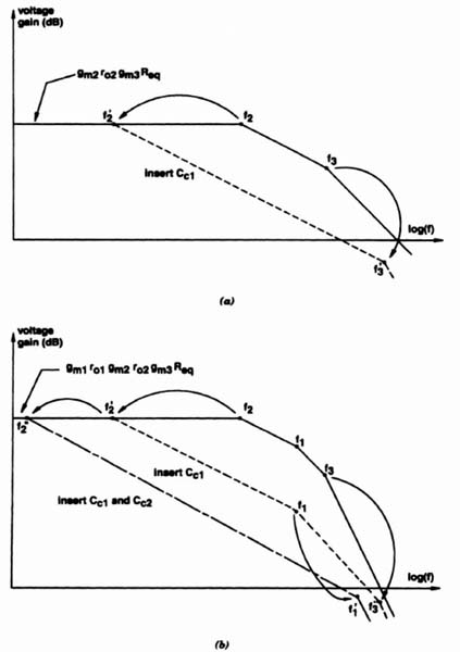
Figure 4.32. (a) Frequency response of the intermediate and output stages before and after inserting Cc1 (b) frequency response of the complete three-stage op-amp before and after inserting the nested Miller compensation capacitors Cc1 and Cc2.

Figure 4.33. Loss and phase responses of the op-amp of Fig. 4.10 for two different values of the load capacitance CL.
In addition, the compensation in this circuit is achieved without coupling high-frequency noise from the power supplies to the output as in multistage op-amps. Hence the high-frequency PSRR can be high.
4.5. DYNAMIC RANGE OF CMOS OP-AMPS
Among the most important characteristics of an op-amp are the input-stage common-mode range (CMR) and the output-stage voltage swing. The input common-mode range specifies the range of the common-mode input voltage values such that the differential stage continues to amplify the differential input voltage with approximately the same differential gain. The output voltage swing is the range over which the output voltage can vary without excessive distortion. Two possible configurations of an op-amp are shown in Fig. 4.34a and b. In Fig. 4.34a the op-amp is used with two external resistors as an inverting buffer. Since one input of the op-amp is connected to ground, the common-mode ac input is zero. In Fig. 4.34b, the op-amp is connected as a unity-gain buffer. All of the ac input signal is now applied as a common-mode input to the op-amp. While the output voltage swing is important for both cases, the input common-mode range is important only for the unity-gain buffer of Fig. 4.34b and is not important for the inverting buffer of Fig. 4.34a.

Figure 4.34. (a) Op-amp circuit without common-mode signal; (b) unity-gain op-amp configuration with common-mode signal.
Figure 4.35 illustrates a p-channel-input CMOS differential stage. This stage will be used as an example to discuss the input common-mode range. The drain-to-source dc voltage of transistor Q1 (and Q2) is given by
The minimum allowable common-mode input voltage occurs when Q1 and Q2 are at the edge of their saturation regions. It can be obtained by setting VDS1 = VDsat1 in Eq. (4.73):

Figure 4.35. A p-channel input CMOS differential stage used to calculate common-mode range.
Since ![]() , the minimum common-mode input voltage is approximately equal to VSS plus the drain-to-source saturation voltage of transistor Q3.
, the minimum common-mode input voltage is approximately equal to VSS plus the drain-to-source saturation voltage of transistor Q3.
A similar analysis can be performed to determine the highest common-mode input voltage. As the input voltage is increased, the drain-to-source voltage of Q5 is reduced. The maximum common-mode voltage is achieved when Q5 is about to leave the saturation region, or VDS5 = VDsat5. The drain-to-source of Q5 is given by
![]() is obtained by setting VDS5 = VDsat5:
is obtained by setting VDS5 = VDsat5:

Since ![]() , and
, and ![]() are all negative, we have
are all negative, we have
Combining Eqs. (4.75) and (4.78), the input common-mode range is found:
Note that typical values are ![]() and |VDsat1| = |VDsat5| = 0.3 V. So from Eq. (4.79) it is clear that while the p-channel input differential stage of Fig. 4.35 has a reasonably good negative common-mode swing, the positive common-mode swing is poor and is limited to at least 1.4 to 1.6 V below the positive power supply voltage. A similar analysis can be carried out for the differential stage with n-channel inputs, shown in Fig. 4.36. The common-mode range can be derived as
and |VDsat1| = |VDsat5| = 0.3 V. So from Eq. (4.79) it is clear that while the p-channel input differential stage of Fig. 4.35 has a reasonably good negative common-mode swing, the positive common-mode swing is poor and is limited to at least 1.4 to 1.6 V below the positive power supply voltage. A similar analysis can be carried out for the differential stage with n-channel inputs, shown in Fig. 4.36. The common-mode range can be derived as
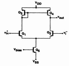
Figure 4.36. An n-channel input CMOS differential stage.

For this case the positive input common-mode limit is approximately one |VDsat3| below the positive supply voltage for ![]() . The negative limit of the input common-mode voltage is 1.4 to 1.6 V above the negative supply voltage. The input common-mode ranges of the two differential stages of Figs. 4.35 and 4.36 are complementary. While the p-channel input differential stage has good negative and poor positive input common-mode swing, the n-channel input has the complementary range. Op-amps with wide positive and negative input common-mode ranges can therefore be obtained using a combination of p- and n-channel differential stages. They are discussed in Section 4.10.
. The negative limit of the input common-mode voltage is 1.4 to 1.6 V above the negative supply voltage. The input common-mode ranges of the two differential stages of Figs. 4.35 and 4.36 are complementary. While the p-channel input differential stage has good negative and poor positive input common-mode swing, the n-channel input has the complementary range. Op-amps with wide positive and negative input common-mode ranges can therefore be obtained using a combination of p- and n-channel differential stages. They are discussed in Section 4.10.
The output voltage swing of the two-stage op-amp is discussed next. Such an op-amp with a p-channel differential input is shown in Fig. 4.37. The output voltage swing is limited by the requirement that transistors Q6 and Q7, must remain in the saturation region. It can be easily shown that this results in the condition
If the output swings beyond the range specified by Eq. (4.81), transistors Q6 and Q7 will leave the saturation region, reducing the gain of the output stage. Further increase of the output voltage will be limited by the power supply voltages.
A single-stage folded-ease ode op-amp with p-channel input devices and an improved biasing scheme was discussed earlier and was shown in Fig. 4.10. First, consider the lower limit of the input common-mode range. With the improved biasing scheme, transistors Q5 and Q6 are biased slightly above the saturation region, so
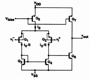
Figure 4.37. Two-stage CMOS op-amp.
As before, the drain-to-source voltage of Q1 is given by
Setting VDS5 = VDsat5 and ![]() in Eq. (4.83), we have
in Eq. (4.83), we have
For Q1 at the edge of saturation, the minimum value of VDS1 is VDsat1:
Rearranging yields
Since VTP < 0 and VDsat5 > 0. can rewrite Eq. (4.86) as
Normally, ![]() . Hence
. Hence ![]() , and the input common-mode signal can go below VSS.
, and the input common-mode signal can go below VSS.
To find the maximum input common-mode voltage, we note that the performance of the circuit is similar to that of the differential stage shown in Fig. 4.35. This leads to
Since VDsat1, VDsat7 and ![]() are all negative numbers, Eq. (4.88) gives
are all negative numbers, Eq. (4.88) gives
Combining Eqs. (4.87) and (4.89) the input common-mode range can be written as

As Eq. (4.90) shows, the input stage of the single-stage folded-cascode op-amp of Fig. 4.10 has an excellent lower limit for its common-mode range, lower than the negative supply voltage. The upper limit of the common-mode range is, however, by as much as 1.4 to 1.6 V below the positive supply voltage. A complementary cascode op-amp with n-channel input devices will be characterized by excellent positive input common-mode range (which includes the positive supply voltage) and a minimum input common-mode limit that is 1.4 to 1.6 V above the most negative supply voltage.
The op-amp of Fig. 4.10 uses an improved biasing scheme such that both Q6 and Q4 are biased at the edge of saturation:

The maximum output voltage swing was derived earlier and is given by Eq. (4.16). From that equation, the output voltage swing is limited to a range that is at least 2VDsat above VSS and 2VDsat below VDD. Of course, νout, can swing beyond the range described in (4.16); however, as the output crosses the specified upper (lower) limit, first transistors Q2c (Q4c) leave the saturation region, and (as illustrated in Fig. 3.14) the output impedance drops, resulting in a reduction in the overall gain. Further, increase (decrease) of νout causes Q4 (Q6) to leave the saturation region and results in drastic reduction in the output impedance and hence in the gain. In this region the op-amp has very little differentia] gain and the output signal will be severely distorted.
In summary, the single-stage folded-cascode op-amp of Fig. 4.10 has an excellent negative-input common-mode range but a poor positive common-mode range. It has a reasonably wide output voltage swing; the output voltage can reach to within 0.5 to 1 V of the supply voltages without serious distortion or drop in gain.

Figure 4.38. Internally compensated CMOS operational amplifier.
4.6. FREQUENCY RESPONSE, TRANSIENT RESPONSE, AND SLEW RATE OF COMPENSATED CMOS OP-AMPS [9,10]
Next, an approximating frequency- and time-domain analysis of the compensated CMOS op-amp of Fig. 4.38 will be given. For small input signals νin the transistors will operate in their saturation regions, and their small-signal models can be used. Then, for moderate frequencies (i.e., for |sp1| ![]() ω
ω ![]() |sp2|) the input stage Q1 to Q5 can be replaced by a frequency-independent voltage-controlled current source, while subsequent stages, Q6 to Q11, can be replaced by a frequency-independent amplifier with the feedback capacitor Cc connected between its input and output terminals (Fig. 4.39). The model is valid as long as the signal frequencies are much larger than |sp1| but are negligibly small compared to the magnitude of the high-frequency pole sp2. From Fig. 4.39, Vout(s) = gmiVin(s)/sCc, so that the high-frequency gain is given by Aν(jω) = Vout(jω)/Vin(jω) = gmi/jωCc. The unity-gain frequency is thus ω0 = gmi/Cc. For |sp2|
|sp2|) the input stage Q1 to Q5 can be replaced by a frequency-independent voltage-controlled current source, while subsequent stages, Q6 to Q11, can be replaced by a frequency-independent amplifier with the feedback capacitor Cc connected between its input and output terminals (Fig. 4.39). The model is valid as long as the signal frequencies are much larger than |sp1| but are negligibly small compared to the magnitude of the high-frequency pole sp2. From Fig. 4.39, Vout(s) = gmiVin(s)/sCc, so that the high-frequency gain is given by Aν(jω) = Vout(jω)/Vin(jω) = gmi/jωCc. The unity-gain frequency is thus ω0 = gmi/Cc. For |sp2| ![]() ω0, the phase of Aν at ω0 will thus be close to 90°. This can be obtained by choosing Cc sufficiently large.
ω0, the phase of Aν at ω0 will thus be close to 90°. This can be obtained by choosing Cc sufficiently large.
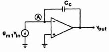
Figure 4.39. Small-signal model of the CMOS op-amp used to calculate its frequency response.

Figure 4.40. Slewing response of the CMOS op-amp connected in the inverting mode: (a) circuit; (b) input signal; (c) small-signal output waveform; (d) large-signal output waveform.
Consider next the voltage inverter shown in Fig. 4.40a. Assume again that the amplifier is compensated, so that its voltage gain can be approximated by
Hence for an input step νin(t) = V1u(t), the output voltage is in the form
(Problem 4.11). Thus, for a square input voltage (Fig. 4.40b) the exponentially varying waveform of Fig. 4.40c should occur at the output.* If the amplitude V1, is small (say, much less than 1 V), this is in fact what happens. If, however, the input voltage is large (e.g., V1 = 5 V), the experimentally observable output voltage is of the form shown in Fig. 4.40d. The nearly linear (rather than exponential) rise and fall of νout(t) is called slewing, and the nearly constant slope dνout/dt of the curve is called the slew rate. Slewing is a nonlinear (large-signal) phenomenon, and hence it must be analyzed in terms of the large-signal model of the op-amp shown in Fig. 4.41. Prior to the arrival of the input step, νin = 0, and the currents in Q1 and Q2 are both equal to Io/2. After the large step occurs at the input, Q1 conducts more current and cuts off Q2. Hence the current conducted by Q1 and Q3 is now Io (Fig. 4.41). Since Q3 and Q4 form a current mirror, the current in Q4 (which charges Cc) is also Ic. Assuming that the output stage A2 can sink the current Io, the slew rate is
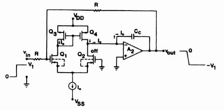
Figure 4.41. Large-signal model for calculating the slew rate of a CMOS op-amp in the invening mode.
where Qc is the charge in Cc. Here Cc = gmi/ω0, where [from Eq. (2.18)] the transconductance of the input stage is
and ω0 is the unity-gain frequency of the op-amp. Combining these relations, we obtain
Thus the slew rate can be increased by increasing the unity-gain bandwidth and the bias current of the input stage, and by decreasing the W/L ratio of the input transistors.
It should be noted that the transconductance of MOSFETs is much lower than that of bipolar devices. This is ordinarily a major disadvantage; however, it results in significantly higher slew rates for MOS op-amps than for bipolar ones for a given unity-gain bandwidth since Cc can be smaller.
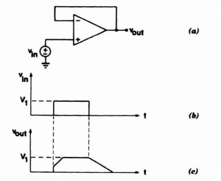
Figure 4.42. Slewing in a voltage follower: (a) op-amp used as a voltage follower; (b) large input signal; (c) output response.
The negative slewing of νout continues until it reaches −V1. At that time the gate voltage of Q1 [which, due to the two resistors R, equals (νin + νout)/2] reaches zero voltage. Hence at that time the quiescent bias conditions are restored, and Q1 to Q4 all carry a current Io/2. Therefore, the charging of Cc and the decrease of the output voltage cease.
The complementary process takes place when νn drops back to zero at t = t2. Now Q1 cuts off, since νout = −V1 still holds and hence its gate voltage drops to −V1/2. Thus Q3 and Q4 cut off, and Cc is discharged through Q2 with a current Io, provided that A2 can source at least the same current. The slew rate of νout is hence again Io/Cc. The process stops when νout, (and hence the gate voltage of Q1) reaches zero voltage.
In Fig. 4.41, the op-amp operates in the inverting mode. Figure 4.42a illustrates the use of the op-amp as a unity-gain voltage follower. Figure 4.42b shows an input pulse waveform; Fig. 4.42c shows the corresponding output response under large-signal conditions. As the diagram shows, the rising edge contains a positive step followed by a fast slewing rise, while the falling edge is a relatively slow linear slope.
The behavior of the rising edge can be understood by considering the equivalent circuit shown in Fig. 4.43. In the circuit, the stray capacitance Cw across the input-stage current source Io is included. Note that Cw is quite large in CMOS op-amps where the common sources of the input devices Q1 and Q2 are connected to the p-well, since this creates a large capacitance between the source and the substrate.
A large input signal νin(t) = V1u(t) turns Q2 fully on. Therefore its source voltage νw rises and hence Q1 and Q3 are turned off. Thus Q2 carries the full current Io + iw, where iw(t) is the current through Cw. Since normally the combined impedance of Cw. and the current source Io is much larger than the driving impedance (1/gm2) of Q2, the incremental source voltage is νw(t) ≈ νin(t). Hence
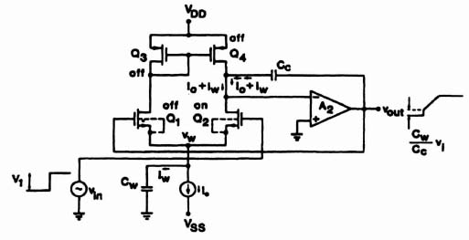
Figure 4.43. Equivalent circuit of the voltage follower used to calculate the large-signal behavior for positive inputs.
which is the impulse function V1Cw δ(t). The output voltage satisfies

The first term represents the linear rise, with a slew rate Io/Cc, while the second represents the small pedestal seen at the beginning of the rising edge.
For a negative step, the equivalent circuit of Fig. 4.44 applies. Now the input signal turns Q2 off, and Q1, Q3, and Q4 all carry the current Io − iw. Considering next the two capacitors Cc and Cw, we note that Cc is connected between νout(t) and (virtual) ground, while Cw is connected between νw and (true) ground. Now νw(t) follows the gate voltage νout(t) of Q1, and hence νw ≈ νout, so that

Therefore, iw = IoCw/(Cc + Cw) and
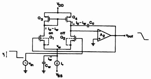
Figure 4.44. Equivalent circuit of the voltage follower used to calculate the large-signal behavior for negative inputs.
Thus the negative slew rate is reduced by the presence of Cw, from Io/Cc to Io/(Cc + Cw), that is, by a factor 1 + Cw/Cc.
4.7. NOISE PERFORMANCE OF CMOS OP-AMPS
Noise represents a fundamental limitation of the performance of MOS op-amps: the equivalent noise voltage may be several times greater than a comparable bipolar amplifier. The noise performance of an MOS op-amp is due to both thermal and 1/f noise sources. The dominating noise source depends on the frequency range of interest. At low frequencies the 1/f noise dominates, whereas at high frequencies the thermal noise is more important and the 1/f noise can be ignored. Hence it is important to analyze the causes of noise and the possible measures that can reduce it. As an example, the noise of a two-stage CMOS op-amp will be analyzed and the noise contribution of each transistor to the total input referred noise will be presented. A similar analysis can be carried out for folded cascode or other types of op-amps.
Figure 4.45 shows an uncompensated CMOS op-amp, with the noise generated by each device Qi represented symbolically by an equivalent voltage source νni connected to its gate.* (The calculation of the gate-referred noise voltages νni was described briefly in Section 2.7.) We can next combine the noise sources νn1 to νn4 in the differential input stage into a single equivalent source νnd connected to the input of an otherwise noiseless input stage, as shown in Fig. 4.46. (Note that the noise of Q5 is a common-mode signal and is hence suppressed by the CMRR of the op-amp; it is therefore omitted in Fig. 4.45.) The voltage gain from the noise sources νn1 and νn2 to the output node A of the input stage can be calculated using its low-frequency equivalent circuit. This gives
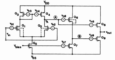
Figure 4.45. Noise sources in a CMOS operational amplifier.
This is the same as the differential signal gain of the stage. Similarly, the gain between sources νn3 and νn4 and node A can be calculated. Physically, the noise source νn3 introduces a noise current gm3νn3 into Q3, which is mirrored in Q4. Hence νn3 causes currents of Q3 and Q4 to change by gm3νn3, and thus νA by gm3νn3/(gd2 + gd4). The effect of νn4 is similar. The gain is therefore
Figure 4.46. Block diagram of a three-stage CMOS operational amplifier with noise sources.
Since these sources are all uncorrelated, they result in a mean-square voltage
at node A. Hence the equivalent input noise voltage νnd = νA/Ad has the mean-square value
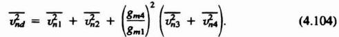
Hence, to minimize ![]() clearly νn1 and νn2 should be small and gm4
clearly νn1 and νn2 should be small and gm4 ![]() gm1. The former, by the discussions of Section 2.7, requires that the area (W/L) and transconductance (gm) of Q1 and Q2 be large. To obtain large gm, the bias current and W/L ratio should be large—this, however, requires large devices and high power dissipation.
gm1. The former, by the discussions of Section 2.7, requires that the area (W/L) and transconductance (gm) of Q1 and Q2 be large. To obtain large gm, the bias current and W/L ratio should be large—this, however, requires large devices and high power dissipation.
The noise contribution of the load devices can be reduced, as (4.104) shows, by making their transconductances as small as their biasing conditions permit. This can be achieved by increasing their lengths L. Thus, assuming that the areas of the input and load devices are given, the W/L ratios of the input devices Q1 and Q2 should be as large, and those of the load devices Q3 and Q4 as small as other considerations permit. Also, it has been found experimentally [11] that the rms equivalent 1/f noise voltage νn is about three times larger for an n-channel device than for a p-channel device. Since in Eq. (4.104) (gm4/gm1)2 ![]() 1, it is hence advantageous to use p-channel input devices with n-channel loads, rather than the other way around, as shown in Fig. 4.45. Applying all these principles, the equivalent input noise voltage νnd can be reduced appreciably [11].
1, it is hence advantageous to use p-channel input devices with n-channel loads, rather than the other way around, as shown in Fig. 4.45. Applying all these principles, the equivalent input noise voltage νnd can be reduced appreciably [11].
Similarly, the noise sources of the source follower (Q6, Q7) can be replaced by an equivalent source νns (Fig. 4.46). From the low-frequency small-signal equivalent circuit,

Referring check to the input of the op-amp, the total equivalent input noise voltage becomes

For low frequencies where ![]() , the effect of νns is negligible; however, at higher frequencies this will no longer be true. Since Q6 and Q7 are used as a level shifter, the gate–source voltage drop of Q6 must be large. By Eq. (2.9) this will be achieved for a given iD6 if k6 = k' (W/L)6 is small. Hence Q6 is a long thin device, and (gm7/gm6)2
, the effect of νns is negligible; however, at higher frequencies this will no longer be true. Since Q6 and Q7 are used as a level shifter, the gate–source voltage drop of Q6 must be large. By Eq. (2.9) this will be achieved for a given iD6 if k6 = k' (W/L)6 is small. Hence Q6 is a long thin device, and (gm7/gm6)2 ![]() 1. At frequencies where |Ad(ω)| ≈ gm7/gm6, the effect of νn7 is comparable to that of νn1 and νn2. Hence care must be taken in the design of Q7 to make it a low-noise device.
1. At frequencies where |Ad(ω)| ≈ gm7/gm6, the effect of νn7 is comparable to that of νn1 and νn2. Hence care must be taken in the design of Q7 to make it a low-noise device.
The effect of the noise sources νn8 and νn9 can be analyzed similarly and can be represented by an equivalent source νn0. However, they usually do not affect the total equivalent input noise voltage significantly.
Normally, all νni contain a 1/f noise component that dominates it at low frequencies. Hence the equivalent input noise voltage is greatest at low frequencies (below 1 kHz), where |Ad(ω)| ![]() 1. Thus the input devices Q1 and Q2 tend to be the dominant noise sources, and their optimization is the key to low-noise design.
1. Thus the input devices Q1 and Q2 tend to be the dominant noise sources, and their optimization is the key to low-noise design.
Using chopper-stabilized differential configuration, the low-frequency 1/f noise of the op-amp can be canceled, and a large (over 100 dB) dynamic range obtained for an integrated MOS low-pass filter. For wide-band operational amplifiers and a low clock frequency, aliasing can increase the effect of the high-frequency noise to the point where it overwhelms the 1/f noise. Hence the unity-gain frequency ω0 should be kept as low as is permitted by the application at hand.
4.8. FULLY DIFFERENTIAL OP-AMPS
In cases when power supply and substrate noise rejection is an important consideration, the use of fully differential (balanced) signal paths may be advantageous. In such circuits the input voltages are symmetrical with respect to the common-mode input voltage Vcmi, and the output voltages are symmetrical with respect to the common-mode output voltage Vcmo. This allows the designer to choose the values of input and output common-mode voltages (Vcmi and Vcmo) independently, for optimum performance. Although for maximum swing, Vcmo should be equal to half the total supply voltage, the same may not be the case for Vcmi. This makes the design of fully differential circuits more complicated and the required chip area 50 to 100% larger than the single-ended realization of the same network. However, there are many compensating advantages in terms of noise immunity. In fully differential op-amps, power supply and substrate noise appear as common-mode signals and are hence rejected by the circuit. In addition, as will be shown, the effective output voltage swing is doubled by the balanced op-amp configuration, while the input circuit (and hence most of the noise) remains the same as for the single-ended op-amps.
Additional advantages also exist. Figure 4.47 shows the circuit of a fully differential switched-capacitor (SC) integrator. In this circuit the switches illustrated schematically in the figure introduce a clock-feedthrough noise into the circuit. This can be minimized by the differential configuration, since (just as the power supply noise) it will appear as a common-mode signal. The symmetry of the circuit should be fully preserved in the physical layout to obtain good rejection of common-mode signals even in the presence of stray elements and nonidealities. The differential configuration also eliminates systematic offset voltages.
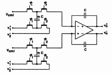
Figure 4.47. Fully differential switched-capacitor integrator.
The noise rejection properties of the fully differential circuits in actual implementation are not as effective as the theory predicts. This is partly because the noise coupled from the power supplies or substrate is not fully symmetrical. Also the clock-feedthrough noise from switches has a voltage-dependent component that couples to one signal path more than the other. However, by using careful and symmetrical layout methodologies it is almost guaranteed that the noise rejection properties of fully differential circuits are far superior than those of single-ended designs.
The circuit diagram of a fully differential single-stage folded-cascode op-amp is shown in Fig. 4.48. This circuit is obtained by modifying the op-amp of Fig. 4.10 and replacing the p-channel current mirrors with two cascode current sources Q3. Q3c and Q4, Q4c. Figure 4.49 shows an alternative two-stage fully differential op-amp [12]. The differential input stage consists of transistors Q1A, Q1B, Q2A, Q2B, Q9A, Q9B, and Q5. The common-gate devices Q9A and Q9B have been added to increase the gain of the operational amplifier and to reduce the differential input capacitance. The two differential output stages are formed with the two common-source amplifiers, consisting of transistors Q3A, Q4A, Q4B and Q4B. A common-mode feedback (CMFB) circuit has been added to both op-amps. The CMFB circuit takes its inputs from the differential output of the op-amp and provides a common-mode feedback signal. This is necessary, since in a fully differential op-amp the common-mode output voltage must be internally forced to ground or to some other reference potential. By contrast, in a single-ended op-amp one of the input terminals is usually grounded and the other becomes virtual ground due to an externally applied negative feedback. This stabilizes the common-mode voltages at both input and output terminals.

Figure 4.48. Circuit diagram of a fully differential single-stage folded-cascode op-amp.

Figure 4.49. Circuit diagram of a two-stage fully differential op-amp.
One of the main drawbacks associated with the fully differential op-amp is the need for the CMFB circuit. Besides requiring extra area and power, the CMFB circuit limits the output swing, increases noise, and slows down the op-amp. The design of a good CMFB circuit is one of the most complicated parts of the fully differential op-amp design. There are two major design approaches for the CMFB circuits, the switched-capacitor approach [13] and the continuous-time approach [12,14]. The switched-capacitor approach is normally used in switched-capacitor circuits, while the continuous-time approach is used in non-sampled-data applications.
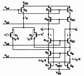
Figure 4.50. Fully differential folded-cascode op-amp with continuous-time CMFB circuit.
Figure 4.50 shows the single-stage fully differential folded-cascode op-amp of Fig. 4.48 with a continuous-time CMFB circuit added [15,16]. The common-mode feedback operates the following way. Since the gate voltages of Q5 and Q6 are fixed at Vb1 and their currents are I + Io/2, their source voltages are also stabilized. This fixes the drain-to-source voltages νDS7 and νDS8 of Q7 and Q8. The value of Vb1 is chosen such that |νDS7| ![]() VDsat, so that both Q7 and Q8 operate in their linear (ohmic) regions. Their aspect ratios (W/L)7 = (W/L)8 are chosen such that in equilibrium the common-mode output voltage
VDsat, so that both Q7 and Q8 operate in their linear (ohmic) regions. Their aspect ratios (W/L)7 = (W/L)8 are chosen such that in equilibrium the common-mode output voltage ![]() has some desired value (usually, ground potential). If the common-mode voltage νout,c would now drop for any reason, the resistance of Q7 and Q8 increases. This reduces |νGS5| and |νGS6|, and since the current in Q5 and Q6 remains unchanged, it forces |νDS5| and |νDS6| to increase. Thus the drain voltages of Q5 and Q6 rise. This, by the argument just presented, reduces |νGS1c| and |νGS2c| and thus increases their drain voltages, which are
has some desired value (usually, ground potential). If the common-mode voltage νout,c would now drop for any reason, the resistance of Q7 and Q8 increases. This reduces |νGS5| and |νGS6|, and since the current in Q5 and Q6 remains unchanged, it forces |νDS5| and |νDS6| to increase. Thus the drain voltages of Q5 and Q6 rise. This, by the argument just presented, reduces |νGS1c| and |νGS2c| and thus increases their drain voltages, which are ![]() and
and ![]() . The common-mode voltage νout,c is thus increased. The gain of the negative feedback loop is readily seen to be
. The common-mode voltage νout,c is thus increased. The gain of the negative feedback loop is readily seen to be ![]() , which can be very high. This feedback loop also stabilizes νout,c against transistor parameter variations arising from fabrication imperfections.
, which can be very high. This feedback loop also stabilizes νout,c against transistor parameter variations arising from fabrication imperfections.
Since Q7 and Q8 operate in their linear (ohmic) regions, their drain currents are linear functions of their gate voltages. Thus it can readily be shown (Problem 4.16) that a differential voltage ±ν at the output terminals does not affect the overall drain–source resistance of the parallel combination of Q7 and Q8. Thus the common-mode output voltage does not change if a differential input signal is applied; this is, of course, a desirable feature.
Using small-signal analysis, it can be shown (Problem 4.17) that the differential gain of the stage is
where Ro is the output impedance at either output node:
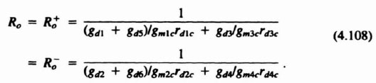
Since the circuit is a folded cascode, it does not require a level shifter. Also, since the desired output is a differential signal, no differential-to-single-ended conversion is required. Thus the nondominant poles introduced by these stages do not appear. The only high-impedance nodes are the output terminals, and the corresponding dominant poles are those due to the time constants ![]() and
and ![]() , where
, where ![]() and
and ![]() are the load capacitances at the output terminals. To achieve compensation, the dominant poles can hence be shifted to lower frequencies by increasing
are the load capacitances at the output terminals. To achieve compensation, the dominant poles can hence be shifted to lower frequencies by increasing ![]() and
and ![]() . Since no internal compensation is required, the op-amp can have a fast settling time and is hence well suited for the implementation of high-frequency switched-capacitor filters.
. Since no internal compensation is required, the op-amp can have a fast settling time and is hence well suited for the implementation of high-frequency switched-capacitor filters.
Since the output impedances of the circuit can be made very high, the dc differential gain AD can be large, comparable to that of a basic two-stage op-amp. A possible bias chain circuit for the op-amp of Fig. 4.50 is shown in Fig. 4.51. Choosing I = Io/2, the aspect ratios can be found as
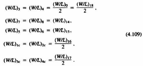
(W/L)19 should be chosen (in conjunction with the other aspect ratios in the bias chain) to set Io to its desired value. For this bias circuit with the aspect ratios given above, the dc currents of Q7, Q8, and Q14 are equal. Also, their dc drain voltages are approximately the same. Hence their gate-to-source dc bias voltages satisfy
This shows that VG7 = VG8 ![]() VG14 = Vcm. Thus the output common-mode voltage is equal to Vcm when this bias circuit is designed using Eq. (4.109).
VG14 = Vcm. Thus the output common-mode voltage is equal to Vcm when this bias circuit is designed using Eq. (4.109).

Figure 4.51. Bias chain for the fully differential op-amp of Fig. 4.50.
An alternative form of continuous-time common-mode feedback circuit is shown in Fig. 4.52 [17, pp. 287–291]. This circuit can be used to provide common-mode feedback for the folded-ease ode differential op-amp of Fig. 4.48. The feedback voltage VFB will bias transistors Q3 and Q4. In the absence of a differential voltage ![]() transistors Q8, Q9, Q12, and Q13 will carry currents equal to I/2 and Q15 will have a current equal to I. The current of Q15 will be mirrored into Q3 and Q4, which will set the output current of the differential op-amp. The common-mode feedback therefore forces Q8 and Q13 to have the same gate–source voltages as Q9 and Q12, forcing the common-mode output of the op-amp to Vcm. In the presence of a differential voltage, as long as (
transistors Q8, Q9, Q12, and Q13 will carry currents equal to I/2 and Q15 will have a current equal to I. The current of Q15 will be mirrored into Q3 and Q4, which will set the output current of the differential op-amp. The common-mode feedback therefore forces Q8 and Q13 to have the same gate–source voltages as Q9 and Q12, forcing the common-mode output of the op-amp to Vcm. In the presence of a differential voltage, as long as (![]() has a value that is exactly the negative of
has a value that is exactly the negative of ![]() (with respect to Vcm), the current in Q8 will increase (decrease) while the current in Q13 will decrease (increase), keeping the current in Q15 unchanged. The common-mode voltage will be kept close to Vcm as long as the differential voltage is not so large that the transistors in the common-mode feedback circuit (Q8, Q13) turn off. The sizes of the transistors in the differential pair can be selected in such a way that their gate-source voltages are maximized, hence extending the operating range. The input range, however, is a major limitation of this circuit.
(with respect to Vcm), the current in Q8 will increase (decrease) while the current in Q13 will decrease (increase), keeping the current in Q15 unchanged. The common-mode voltage will be kept close to Vcm as long as the differential voltage is not so large that the transistors in the common-mode feedback circuit (Q8, Q13) turn off. The sizes of the transistors in the differential pair can be selected in such a way that their gate-source voltages are maximized, hence extending the operating range. The input range, however, is a major limitation of this circuit.
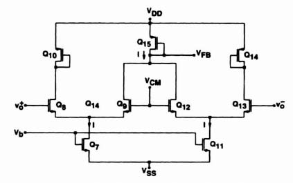
Figure 4.52. Alternative form of continuous-time CMFB circuit.
Other than the limited input differential range, the common-mode feedback circuits described so far have two additional drawbacks. First the circuit that detects the output common-mode signal has a nonlinear characteristic. Second, the open-loop gain of the common-mode feedback may not be sufficiently large, due to its inherent limitations. The first problem can be avoided by using linear common-mode detectors such as a pair of identical resistors or the corresponding switched-capacitor equivalent for sampled data circuits. To reduce the effect of the second problem, the output common-mode feedback circuit should have a dc gain and bandwidth as large as the respective differential-mode circuitry. This can be accomplished by having the differential and output common-mode paths share as much circuitry as possible, thus treating both signals as equally as possible [12]. These concepts can be applied to the common-mode feedback circuit of the two-stage fully differential op-amp of Fig. 4.49. The complete circuit diagram of the op-amp is shown in Fig. 4.53. The common-mode feedback signal Vc is formed with two equalvalued resistors that are connected between the two differential outputs and is given by ![]() . The common-mode feedback circuit consisting of transistors Q6A, Q6B, Q6C, Q8 and Q7 is merged with the differential-mode circuitry at the very front end of the operational amplifier. Therefore, an equally amplified common-mode feedback signal and differential-mode input signal are combined as currents into the loads Q2A and Q2B. From there on to the outputs, the signals share the same circuitry, including the compensation networks consisting of RCA, CCA, RCB, and CCB. One potential drawback of this circuit is the resistors in the common-mode signal detector, which loads the op-amp differential output stages and hence degrades the amplifier dc gain. This effect can be reduced by designing the output stage transistors Q3A, Q3B, Q4A, and Q4B to have large W/L ratios and large currents, hence increasing their transconductances.
. The common-mode feedback circuit consisting of transistors Q6A, Q6B, Q6C, Q8 and Q7 is merged with the differential-mode circuitry at the very front end of the operational amplifier. Therefore, an equally amplified common-mode feedback signal and differential-mode input signal are combined as currents into the loads Q2A and Q2B. From there on to the outputs, the signals share the same circuitry, including the compensation networks consisting of RCA, CCA, RCB, and CCB. One potential drawback of this circuit is the resistors in the common-mode signal detector, which loads the op-amp differential output stages and hence degrades the amplifier dc gain. This effect can be reduced by designing the output stage transistors Q3A, Q3B, Q4A, and Q4B to have large W/L ratios and large currents, hence increasing their transconductances.

Figure 4.53. Schematic diagram of a two-stage fully differential op-amp with a common-mode feedback circuit.

Figure 4.54. Conceptual representation of the resistive divider common-mode signal detector of Fig. 4.53.
The use of resistive divider common-mode signal detector is shown conceptually in Fig. 4.54. In sampled analog systems such as switched-capacitor circuits, the same method used for processing the differential signals can be used for the common-mode detector circuit. Figure 4.55 shows the symbolic representation of the differential switched-capacitor integrator of Fig. 4.47 with a switched-capacitor common-mode detector. In this circuit a pair of integrating capacitors Cc1 and Cc2 and a pair of switched-capacitor resistors α1Cc1 and α1Cc2 implements the common-mode signal detector. This circuit is equivalent to a parallel RC circuit which takes the average of the two voltages ![]() and
and ![]() . For proper operation, the time constant of the equivalent RC should be much faster than the one in the differential signal path [13,18]. Normally, the sizes of α1Cc1 and α1Cc2 are between one-fourth and one- tenth of that of the nonswitched capacitors.
. For proper operation, the time constant of the equivalent RC should be much faster than the one in the differential signal path [13,18]. Normally, the sizes of α1Cc1 and α1Cc2 are between one-fourth and one- tenth of that of the nonswitched capacitors.
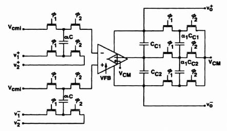
Figure 4.55. Fully differential integrator with switched-capacitor common-mode feedback circuit.

Figure 4.56. Fully differential folded-cascode operational amplifier with switched-capacitor common-mode feedback.
The circuit diagram of a fully differential folded-cascode operational amplifier with switched-capacitor common-mode feedback is shown in Fig. 4.56. The common-mode output level of the amplifier is maintained by the switched-capacitor feedback circuitry. Capacitors C1 and C2 in Fig. 4.56 have equal values and form a voltage divider. A bias voltage is generated across these capacitors based on the average voltage of the differential outputs and is used to control the gates of the NMOS transistors in the output stage (node A). The dc voltages across Cc1 and Cc2 are established by the switched-capacitors α1Cc1, and α1Cc2. These capacitors are first charged between the desired output common-mode voltage and a fixed bias voltage and are subsequently thrown in parallel to Cc1, and Cc2. The fixed bias voltage is equal to the desired voltage used to bias the output-stage current sources. Only changes in the common-mode output are coupled to node A, which returns the common-mode output voltage to the desired level through negative feedback. During the period that the switches controlled by ![]() 1, are on, corrective charges are transferred to Cc1 and Cc2 through the switched capacitors to prevent any drift in the common-mode output voltage. The switched-capacitor common-mode feedback circuit has a wide output voltage swing and is the preferred choice in applications where the op-amp is used in a fully differential circuit involving switched capacitors.
1, are on, corrective charges are transferred to Cc1 and Cc2 through the switched capacitors to prevent any drift in the common-mode output voltage. The switched-capacitor common-mode feedback circuit has a wide output voltage swing and is the preferred choice in applications where the op-amp is used in a fully differential circuit involving switched capacitors.
4.9. CMOS OUTPUT STAGES
The main objective of the output stage of an operational amplifier is to be able to drive a load consisting of a large capacitance (up to several nanofarads) and/or a small resistance (down to 50 Ω or less) with an acceptably low level of signal distortion. It is also desirable to have a large output voltage range, preferably from rail to rail. To achieve the extended voltage swing, the output transistors should be connected in a common-source configuration. In fact, in CMOS operational amplifier design practice a push-pull stage is often used as an output stage, as shown in Fig. 4.57. The push-pull stage consists of two complementary common-source transistors Q1 and Q2, allowing rail-to-rail output voltage swing. The gates of the two output transistors are normally driven by two in-phase ac signals separated by a dc voltage [19,20]. When the input signals are above their corresponding dc values, the drain current of the NMOS device will be larger than the drain current of the PMOS transistor, and hence the output stage pulls a current from the load. If, on the other hand, the input signals are below their dc values, the output stage sources more current than it sinks and thus it pushes a current into the load.
Another important feature of the output stage is the efficiency, which requires a high ratio between the maximum signal current that can be delivered to the load and the quiescent current of the output stage. To achieve this requirement, a class B biasing scheme can be used. Because an output stage using this type of biasing will provide a large output current with a quiescent current that is approximately zero. The drawback, however, is that output stages with class B biasing introduce a large crossover distortion. The distortion can be reduced by using a class A biasing scheme. However, the maximum output current of a class A biased output stage is equal to its quiescent current, which results in poor power efficiency for a rail-to-rail output signal.
A compromise can be achieved between crossover distortion and quiescent power dissipation by using an output stage that is biased between class A and class B. This is called the class AB biasing scheme. In the push-pull output stage of Fig. 4.57, the class AB biasing scheme can be accomplished by keeping the voltage between the gates of the output transistors constant. This principle is shown in Fig. 4.58. To make the quiescent current and the relation between the push and pull currents independent of the supply voltage and process variations, the voltage source VAB in Fig. 4.58 has to track these parameters. Figure 4.59 shows the desired class AB transfer function where the output transistors are biased with a small quiescent current, which improves the crossover distortion compared to a class B biased output stage. Also shown is the maximum output current, which is much larger than the quiescent current and increases the power efficiency compared to a class A biased output stage. To further reduce the crossover distortion, the transistor that is not delivering the output current should be biased with a small amount of residual current. This current will eliminate the turn-on delay of the nonactive output device, hence reducing the crossover distortion [21]. This minimum current is represented by Imin in Fig. 4.59.
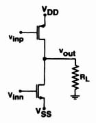
Figure 4.57. Push-pull CMOS output stage with rail-to-rail output swing.
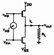
Figure 4.58. Push-pull CMOS output stage with class AB biasing.
Two other important parameters of the push-pull rail-to-rail output stage of Fig. 4.58 are the output voltage range and the maximum output current that is supplied to the load. To determine the output voltage range, first assume that the input signal voltage in Fig. 4.58 is increasing. This will cause the NMOS transistor to pull more current from the load, and thus the output voltage decreases. This process continues until the NMOS device ends up in the triode region and the output voltage becomes limited. The same happens for the PMOS device when the input signal decreases. The output voltage swing can be extended by maximizing the gate-to-source voltage swing and by choosing the largest possible W/L ratio for the output devices. The allowable gate-to-source voltage drive and the dimensions of the output transistors also determine the maximum output current of the output stage. In conclusion, an adequately designed class AB output stage should allow the gate-to-source voltage of the output transistors to get as close to the supply rails as possible.

Figure 4.59. Output-stage current for class AB biasing.

Figure 4.60. Multistage low-output-impedance op-amp.
Operational amplifiers that are required to drive a heavy load at the output (especially a small resistance) use a multistage structure, as shown in Fig. 4.60 [22]. The first stage is typically a transconductance preamplifier, which provides differential input and a large gain. The output stage is a class AB biased push-pull circuit that provides low output impedance and a large current-driving capability. In the following a variety of output stages are presented and discussed.
The first circuit considered is shown in Fig. 4.61 [22]. For a zero applied differential input signal ![]() , the two matched current sources I, made of devices Q10 and Q11, uniquely define the circuit quiescent current level. For simplicity let us assume that the four NMOS input transistors Q1, Q2, Q5, and Q6 and the four PMOS input transistors Q3, Q4, Q7, and Q8 are identical devices. Then VGS1 = VGS2 = VGS5 = VGS6 and VGS3 = VGS4 = VGS7 = VGS8, which results in I1 = I2 = I. Under this condition the current in output devices Q14 and Q15 is also determined by the current source devices Ql0 and Q1 and the W/L ratio of the two current mirrors Q12, Q14 and Ql3, Q15. It follows, therefore, that the class AB biasing scheme makes the quiescent power consumption of the circuit be controlled precisely by the two matched current sources in the input stage.
, the two matched current sources I, made of devices Q10 and Q11, uniquely define the circuit quiescent current level. For simplicity let us assume that the four NMOS input transistors Q1, Q2, Q5, and Q6 and the four PMOS input transistors Q3, Q4, Q7, and Q8 are identical devices. Then VGS1 = VGS2 = VGS5 = VGS6 and VGS3 = VGS4 = VGS7 = VGS8, which results in I1 = I2 = I. Under this condition the current in output devices Q14 and Q15 is also determined by the current source devices Ql0 and Q1 and the W/L ratio of the two current mirrors Q12, Q14 and Ql3, Q15. It follows, therefore, that the class AB biasing scheme makes the quiescent power consumption of the circuit be controlled precisely by the two matched current sources in the input stage.

Figure 4.61. Schematic of class AB amplifier.
When the differential input signal is positive ![]() , the voltage drop across Q2 and Q3 is increased by
, the voltage drop across Q2 and Q3 is increased by ![]() , while the drop across Q1 and Q4 is decreased by the same amount. Consequently, the current through Q13 is increased while the current in Q12 is reduced close to zero, and a current much larger than the quiescent level, determined by the W/L ratio of Q13 and Q15, is available through Q15 to be delivered to the load.
, while the drop across Q1 and Q4 is decreased by the same amount. Consequently, the current through Q13 is increased while the current in Q12 is reduced close to zero, and a current much larger than the quiescent level, determined by the W/L ratio of Q13 and Q15, is available through Q15 to be delivered to the load.
The peak value for currents I1, and I2 and hence the output current is a function of the applied input voltage. In practice, however, as the current level increases, the sum of the voltage drops across Q1, Q4, and Q12 (Q3, Q2, and Q13) also increases, until it is equal to the total supply voltage. At this point devices Q1 and Q4 (Q2 and Q3) or both enter the linear region of operation, and the current level becomes practically constant independent of the applied input voltage.
The circuit of Fig. 4.61 can be used as a stand-alone single-stage op-amp. It is also suitable for a differential output op-amp since it can produce a complementary output simply by adding two additional current mirrors symmetrical with respect to Q12, Q14 and Q13, Q15. Figure 4.62 shows the entire fully differential amplifier schematic where cascode transistors can be added to the output stage to increase the output impedance and hence the gain [14]. A common-mode feedback should be added to Vcm in Fig. 4.62 for proper operation. The amplifier of Fig. 4.61 can also be used as the output section for a two-stage amplifier. Figure 4.63 shows the schematic of a two-stage low-output-impedance op-amp, where the first-stage transconductance amplifier is made of a simple folded-cascode differential amplifier. Note that in this configuration one input of the differential output stage is connected to an appropriate dc potential (Vbias4), such as halfway between the two supplies. It is also possible to connect the differential input of the output stage to the differential output of a fully differential folded-cascode transconductance amplifier. This is shown in Fig. 4.64, where a common-mode feedback is used to stabilize the differential output of the first stage [14]. This technique is discussed in more detail later in the section.

Figure 4.62. Simplified schematic of fully differential op-amp.

Figure 4.63. Two-stage low-output-impedance op-amp.
A simplified version of the class AB output stage of Fig. 4.61 is shown in Fig. 4.65a [23]. Compared to the amplifier of Fig. 4.61, the positive input and all the corresponding devices are eliminated. The input νin is intentionally biased one VGS below the positive supply and it directly drives the gate of the p-channel output device. The n-channel output transistor is driven by the output of the common-gate amplifier, consisting of devices Q12, Q13, and Ql4. Assuming that
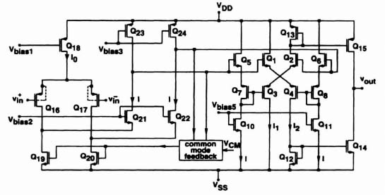
Figure 4.64. Alternative form of two-stage low-output-impedance op-amp.

Figure 4.65. (a) Class AB output stage; (b) wideband class AB output stage.
and
Also, from Eqs. (4.111)–(4.114) and Eq. (4.115) it is clear that in quiescent conditions
Under these conditions, the bias voltage of νin is set to VDD − VGS15. The input νin voltage vin in the negative direction can swing from VDD − VGS18 all the way down to VSS, causing Q18 to provide a large sourcing current. The maximum sourcing current is given by
In the positive direction, νin can swing from VDD − VGS18 to VDD. The maximum sinking current is given by

where ki = ![]() (W/L).
(W/L).
Referring to Fig. 4.65a, the operation of the circuit is as follows. To source an output current, νin goes low and drives the gate of Q18 more negative, which increases its drain current. At the same time, the output of the positive-gain common-gate amplifier consisting of devices Q12, Q13, and Q14 also goes low, reducing the current of Q19. To sink current, νin goes high; it shuts off Q18 by reducing its gate drive and also pulls the gate of Q19 high, which in turn increases its drain current. The maximum source and sink currents are given by Eqs. (4.119) and (4.120).
To drive small resistive loads, the devices used in the output stage are very large. Since the transistor parasitic capacitances increase much faster than its transconductance, the frequency response of the output stage and therefore the entire op-amp deteriorates. More specifically, as a result of a dramatic increase in CGS9, the nondominant pole at node A moves closer to the dominant pole and hence makes the frequency compensation very difficult. An alternative wideband circuit is shown in Fig. 4.65b, where a source follower Q21, has been added to bias node A, and the impedance has been reduced from 1/gm14 in Fig. 4.65a to 1/gm21, in Fig. 4.65b.
The complete circuit schematic of the two-stage low-output-impedance op-amp that uses the output stage of Fig. 4.65b is shown in Fig. 4.66. The input transconductance stage is made of a folded-cascode differential amplifier. The bias current is set by resistor RB and the three diode-connected devices Q31 to Q33, which are connected in series between VDD and the negative supply. The frequency response of the circuit exhibits several real poles. It has two dominant poles, which are due to the output impedance and the corresponding load capacitances of the folded-cascode differential amplifier and the output stage. The remaining nondominant poles are at nodes A to H, which are located at much higher frequencies than are the dominant poles. This is because the impedance levels at all these nodes are determined by the 1/gm value of a large MOS device, which is much smaller than the output impedance at the two nodes that determine the two dominant poles. The op-amp therefore can be compensated using the Miller capacitance Cc in series with a zero-nulling NMOS device operating in triode region, which is connected between the two high-impedance nodes.
Another approach for a class AB push-pull output stage is illustrated in Fig. 4.67 [24], Here the two large common-source output transistors Q1 and Q2 are driven by two error amplifiers, A1 and A2. The feedback loop around A1 (A2) and Q1 (Q2) ensures low output impedance. In this configuration the error amplifiers must satisfy a number of requirements for proper operation of the output stage. First, since the error amplifiers have an input-referred dc offset voltage on the order of several millivolts, they must have a reduced value of open-loop gain on the order of 10. Otherwise, in the case of a large gain, the input referred offset voltage, when referred to the output, will cause unacceptable variations of the quiescent currents in Q1 and Q2. A second requirement is that the error amplifiers must have a rail-to-rail output and input swing so that they can provide good drive capability for the output transistors. Finally, they must be broadband, to prevent crossover distortion. This may become difficult to achieve, however, due to stability constraints.
An alternative form of the output stage of Fig. 4.67 can be achieved by considering the CMOS class AB complementary source-follower stage of Fig. 4.68, which is a direct analog of its bipolar counterpart. In the circuit, Q1 and Q4 form a gain stage, while Q5 and Q6 drive the load RL and Q2 and Q3 provide a voltage drop between the gates of Q3 and Q6 to reduce crossover distortion. The sizes of Q2 and Q3 are chosen such that the gate-to-source voltages of Q5 and Q6 are slightly larger than their threshold voltages. The primary drawback of this circuit is that the gate-to-source voltage of the output transistors limits the output voltage swing. The maximum output voltage for RL → ∞ is VDD − VT5 and the minimum is VSS − |VT6|, where VT5 (VT6) is the threshold voltage of Q5 (Q6). If RL draws current from, say, Q5, the device must provide a drain current νout/RL and hence needs a gate-to-source voltage ![]() . This increases rapidly with decreasing RL and hence represents an important limitation on the achievable positive output voltage swing. Similar considerations hold, of course, for negative swings, due to the necessary VGS6.
. This increases rapidly with decreasing RL and hence represents an important limitation on the achievable positive output voltage swing. Similar considerations hold, of course, for negative swings, due to the necessary VGS6.

Figure 4.66. Two-stage low-output-impedance op-amp that uses the output stage of Fig. 4.65b.
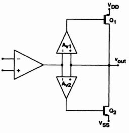
Figure 4.67. Block diagram of CMOS op-amp with class AB push-pull output stage.
Many of the problems of the output stages of Fig. 4.67 and 4.68 are easily solved by merging the two output stages as shown in Fig. 4.69. The problem of quiescent current control is solved by deliberately introducing an offset voltage into A1 and A2 in such a way that transistors Q7 and Q8 are not carrying any current in the quiescent state. Transistors Q5 and Q6 therefore control the quiescent output current. The quiescent output current will be proportional to the current through Q2 and Q3 and is a function of the W/L ratios of Q5 to Q6 and Q6 to Q2. In steady state the class AB circuit consisting of transistors Q5 and Q6 carries the entire output current. The class B output stage, consisting of op-amps A1 and A2, has a very large current-driving capability but is kept off in quiescent conditions. When driving small resistive loads, the class B output stage takes over operation of the stage.
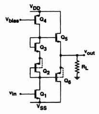
Figure 4.68. CMOS class AB push-pull output stage based on the traditional bipolar implementation.
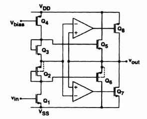
Figure 4.69. Combined class AB and class B output stage.
Besides their usefulness in quiescent current control, transistors Q5 and Q6 provide a high-frequency feedforward path from the input to the output of the push-pull stage and reduce the excess phase shift introduced by op-amps A1 and A2. The op-amps still require some nominal phase compensation to make them stable in the closed-loop unity-gain mode. The frequency characteristic of the overall amplifier is determined largely by Q5 and Q6 rather than that of the composite output stages.
Another class AB biased push-pull output stage is shown in Fig. 4.70 in block diagram form [14]. In this circuit the output stage, consisting of devices Q1 and Q2 is preceded by a fully differential preamplified stage A1. The output stage has several important properties: It has low standby power dissipation, which can be controlled by a supply-independent current source, it has a good current-driving capability, and it has a simple configuration, so it avoids additional parasitic poles. The output stage consists of devices Q1 to Q4, and the quiescent current level at the output stage is controlled by the common-mode voltage of the preamplifier stage. Here since the output stage is driven by a fully differential-output preamplifier stage, an additional common-mode feedback (CMF) is necessary to set the dc voltage values of the differential output (i.e., νo1 = νo2 = Vn = Vb). Therefore, assuming that (W/L)1/(W/L)3 = (W/L)2/(W/L)4, the current Io in the output devices is given by

Figure 4.70. Class AB push-pull output stage with common-mode feedback.

which can be made supply independent.
For this circuit, assuming that the input stage does not impose a limit on the output stage, when it needs to sink the maximum available current, νo1 = Vn can swing all the way up to VDD, resulting in a rail-to-rail gate-to-source voltage drive for Q2. To source current, νo2 swings to VDD, forcing Q4 into the linear region. This in turn causes Vp to move close to VSS, resulting in a large VGS for Q1. Because of the complementary nature of the differential outputs of the input stages when one of the outputs is close to VDD, the other one is close to VSS. As a result, the output stage delivers a push-pull drive to the output transistors Q1 and Q2 in such a way that when one of the devices is heavily conducting, the other one is turned off. Also, since the VGS drives of the output transistors can be as high as the full supply voltage, they can supply a large amount of output current with relatively small device sizes.
The circuit diagram of the complete op-amp is shown in Fig. 4.71. Transistors Q40 to Q47, along with resistor RB, constitute the biasing section. Transistors Q14 to Q25 realize the differential output folded-cascode preamplifier stage. Transistors Q43 and Q46 establish bias voltages for the high-swing cascode current sources. Transistors Q5 to Q13, which establish a bias voltage equal to Vb at the output of the differential stage, achieve the continuous-time common-mode feedback. In the conceptual block diagram representation of the preamplifier stage shown in Fig. 4.70, the common-mode feedback sets the voltage values of the two differential outputs as
In Fig. 4.71 the common-mode feedback is realized by devices Q8 to Q13, while Q5 and the current source Q6 and Q7 generate the bias voltage Vb = VGS5. Devices Q12 and Q13 form a current source that supplies a fixed current to the four source-coupled devices Q8 to Q111. The W/L ratio of Q8 to Q11 are equal; therefore, the tail current is divided equally among the four devices, resulting in equal gate-to-source voltages, so
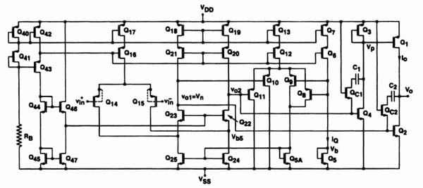
Figure 4.71. Circuit schematic of op-amp with push-pull output stage.
Since the gate potentials of all four devices are equal, the differential output of the preamplifier stage will be biased to Vb. The output stage, consisting of devices Q1 to Q4, is similar to the circuit shown in Fig. 4.70, where the quiescent output current is given by Eq. (4.121).
The open-loop gain of the op-amp is calculated as A = gm14rogm2RL where ro is the output impedance of the preamplifier stage and RL is the load of the output stage. The op-amp can be compensated using two Miller capacitors C1 and C2 along with their zero-nulling MOS resistors, QC1 and QC2. Assuming widely spaced poles, the dominant pole is calculated as

where CM1, = (1 + gm3/gm3) and CM2 = gm2RLC2 [14]. The load capacitance CL, along with the other parasitic capacitances, generate poles and zeros that are above the unity-gain frequency. The common-mode feedback circuit creates a pole-zero doublet which is an order of magnitude below the unity-gain frequency. These are given by
where CM3 = (1 + 2gm10R2)C2 and R2 is the resistance of the zero-nulling MOS device QC2? Since sp1 and sz1 are close to each other, the pole–zero doublet does not cause any instability in the frequency response.
The class AB push-pull output stages presented thus far use elaborate techniques to solve the level-shifting problem between the two signals that drive the output devices and set their quiescent bias currents. A simple, yet very powerful technique that is based on the push-pull stage of Fig. 4.58 is shown in Fig. 4.72 [25]. The circuit consists of the push-pull output stage made of devices Q1 and Q4. In this circuit, transistors Q5 and Q6 form a typical gain stage where the input signal alters the relative conduction levels of the common-gate devices. The class AB bias circuit sets up the two loops, Q1, Q3 and Q2, Q4, that fix the voltage drop between the gates of the output devices.
Referring to Fig. 4.72, the quiescent conditions of the output stage are established as follows. The complementary currents Ib1 and Ib2 (Ib1 = Ib2 = Ib) from the bias generator flow into complementary stacks of diode-connected transistors Q7, Q8 and Q9, Q10 whose drain potentials are used to bias the gates of the common-gate transistors Q3 and Q4. In steady state the current I = 2Ib through transistor Q6 is equally divided between devices Q3, and Q4 so that each one carries a current equal to Ib. Assuming that

Figure 4.72. Rail-to-rail output stage with common-gate level shifters.
and since Q3, Q8 and Q4, Q9 carry the same drain currents Ib, they will have equal gate-to-source voltages and we have V2 = V3 and V1 = V4. As a result Q2, Q10 and Q1, Q7 will also have equal gate-to-source voltages and the steady-state output current is given by

When the output stage is driven to sink a large load current, νin goes low and pulls ν1 and ν2 up to a high level close to VDD. Under this condition Q4 is completely shut off and Q3 carries the full current of I = 2Ib from Q5. The source of Q3 rises to its maximum point, thus cutting back on the conduction of Q1. The drain of the common-gate device Q3 also goes high, hence pulling the gate of Q2 high, making it heavily conductive. Under the conditions of strong sourcing, νin goes high, causing ν1 and ν2 to be pulled low. In this case Q3 is completely shut off and Q4 carries the full current of I = 2Ib. The source of Q4 pulls the gate of Q1 low, hence making it highly conductive.
A complete differential op-amp employing the output stage of Fig. 4.72 is shown in Fig. 4.73. A folded-cascode input stage is used, providing high open-loop gain. The biasing circuit consisting of resistor RB and transistors Q13 to Q21 is designed such that all devices are biased at the onset of their saturation regions, hence maximizing the output voltage swing while providing high gain. The common-gate level-shifter circuit is inserted in the output stage of the folded-cascode differential stage. The op-amp of Fig. 4.73, with an output stage that uses common-gate level shifter to bias the push-pull output devices, is very compact and power efficient and is very suitable for driving small resistive loads.
4.10. OP-AMPS WITH RAIL-TO-RAIL INPUT COMMON-MODE RANGE
In this chapter two generations of CMOS op-amps were presented. The first generation of op-amps was limited to transconductance amplifiers. They had modest performance and were able to drive only capacitive loads. In addition to high-performance transconductance amplifiers, the second generation of these op-amps were able to drive resistive as well as capacitive loads with a level of performance which is compatible to that of their bipolar counterparts. In addition to having a high-performance output stage, third-generation CMOS op-amps have a wide-input common-mode range, which includes the positive and negative power supply rails. The wide- input common-mode range is important for low-voltage applications where the op- amp is connected in a unity-gain buffer configuration.
In an earlier section it was shown that op-amps with p-channel differential stage input devices such as the one in Fig. 4.35 have an input common-mode range that includes the negative power supply. The positive common-mode range is, however, limited to 1.4 to 1.6 V below the positive supply. Op-amps with n-channel input devices have the opposite properties. They have a positive-input common-mode range that includes the positive power supply, whereas the negative range is 1.4 to 1.6 V above the negative supply. For applications where the common-mode input range goes beyond or at least includes both power supply rails, such as the unity-gain buffer shown in Fig. 4.36b, the op-amp requires an input stage with an NMOS and PMOS differential pair connected in parallel. Several op-amp structures with rail-to-rail common-mode input stage are available [14,26]. One example of such an input stage is shown in Fig. 4.74. It has a folded-cascode differential-output structure with common-mode feedback.
The input stage of the op-amp in Fig. 4.74 is constructed from the parallel connection of p- and n-channel differential stages made of transistors Q6 to Q9 and Q26 to Q29, respectively. The differential-stage tail current sources are formed from devices Q6, Q7 and Q28, Q29. They use a cascode structure to increase the output impedance and hence the CMRR, as suggested by Eq. (3.80). High common-mode rejection is important when the op-amp is connected as a unity-gain buffer. Transistors Q40 to Q47 form a simple bias circuit. The two p-channel transistors, Q40 and Q41, combined with resistor RB, generate the reference current. This current is mirrored into transistors Q42 to Q46, which generate the bias voltages for the high-swing cascode current sources. The input stage uses a folded-cascode structure made of transistors Q10 to Q17. An additional common-mode feedback (CMF) circuit sets the dc voltage values of the two differential outputs. The configuration of the common-mode feedback circuit is based on the conceptual block diagram shown in Fig. 4.70. The operation of the common-mode feedback circuit was described in Section 4.9.
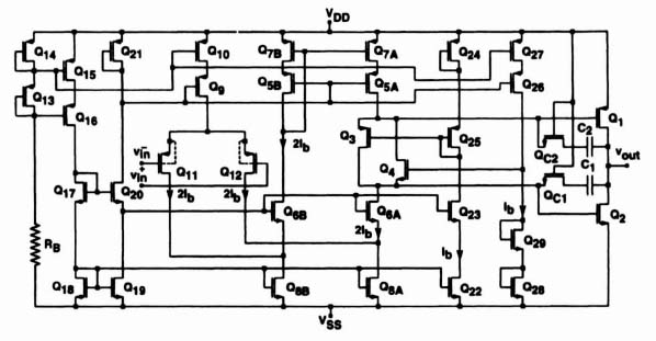
Figure 4.73. Rail-to-rail op-amp using the output stage of Fig. 4.72.
Figure 4.74. Rail-to-rail differential-input/differential-output stage with common-mode feedback.
One major shortcoming of the differential stage of Fig. 4.74 is the fact that a current imbalance occurs in the load device when the common-mode input voltage approaches VDD or VSS. Consider the case when the common-mode voltage approaches VDD. Then as the input devices Q8 and Q9 turn off the current components I that enter the drain of the devices, Q16 and Q17 become zero. This current imbalance causes the drains of Q16 and Q17 to snap to VSS and the op-amp ceases operating in the linear region. To remedy this problem, the circuit is modified by adding transistors Q30 to Q37 (Fig. 4.75) to the input stage and dividing the currents in the devices Q10 and Q11 as well as Ql6 and Q17 into two components: one that is constant and the other that is input dependent. The input-dependent current component becomes zero when their corresponding input pair devices turn off [14,27]. The complete op-amp is shown in Fig. 4.75. Now the sum of currents through the pairs Q10A–Q10B, Q11A–Q11B, Q16A–Q16B. and Q17A–Q17B are normally equal to 2I, while the currents in Q12 to Q15 are equal to I. When the input common-mode voltage approaches VDD (or VSS), devices Q8, Q9 and Q32 (or Q26, Q27, and Q36) cut off and cause the currents through devices Q16A and Q17A (or Q10A and Q11A) to drop to zero. As a result, output voltages νo1 and νo2 remain stable over the complete common-mode input voltage range.
The output stage for the op-amp of Fig. 4.75 is formed from transistors Q1 to Q4. The common-mode feedback circuit sets the quiescent current Io in the output devices to
The class AB push-pull output stage is based on the configuration of Fig. 4.70; its operation was described in Section 4.9.
Frequency compensation for the op-amp is achieved using two Miller capacitors along with their corresponding zero-nulling MOS resistors. The open-loop gain is calculated to be A = (gm8 + gm26)rogm2 where ro is the output impedance of the input stage and RL is the load resistor.
One major drawback of the rail-to-rail op-amp shown in Fig. 4.75 is that the transconductance (gm) of the input devices varies by a factor of 2 over the input common-mode range. This large variation in gm prevents the op-amp from having an optimum frequency compensation over the entire operating range. To keep the transconductance constant, the gm value of the lower and upper parts of the input range should be increased by a factor of 2. This is because in the middle of the common-mode range the gm value of the input stage is the sum of the gm values of the p- and n-channel devices. In the lower common-mode range the n-channel devices turn off and the gm value of the input stage is reduced to the gm value of the p-channel devices. Clearly, the opposite takes place in the upper common-mode range. The gm values of the p- and n-channel input devices are given by

Figure 4.75. Complete rail-to-rail input-stage op-amp.

From the equations above, it can be observed that to maintain a constant gm value, the following condition should be satisfied between the W/L ratios of the p- and n-channel input devices:
As suggested by Eq. (4.131), the gm value of the MOS device is proportional to the square root of its drain current. Therefore, while the p- and n-channel input devices should satisfy the condition of Eq. (4.132), to maintain a constant gm value, the tail currents of the input stages should also vary by a factor of 4 over the input common-mode range. In other words, in the middle of the common-mode range, the p- and n-channel input stages would have tail currents that are equal to Io. In the upper and lower parts of the input range, the tail currents of the p- and n-channel differential stages should be increased to 4Io, respectively. This will maintain an approximately constant gm for the input stage over the entire input common-mode range.
This principle is applied to the circuit shown in Fig. 4.76 [20]. A rail-to-rail input stage is shown, where p- and n-channel differential pairs are placed in parallel. Similar to the op-amp of Fig. 4.75, the stage is able to reach the positive and negative supply rails through the n-channel (Q3–Q4) and p-channel (Q1–Q2) input pairs. The constant-gm, property is achieved by the addition of the current switches Q5 and Q8 and the two current minors Q6–Q7 and Q9–Q10, each with a gain of 3. To better understand the constant-gm, control circuit, the input common-mode range will be divided into three regions.

Figure 4.76. Rail-to-rail folded-cascode constant-gm differential stage.
When the input common-mode goes below Vb3 = (VGS)Q3 + (VDsat)Q20. the n-channel input devices will start turning off and the p-channel input pair will be operational. In this case the n-channel current switch Q5 will turn on while the p-channel current switch Q8 is off. The current of transistor Q5 is multiplied by a factor of 3 and is added to the tail current of the p-channel differential stage. The tail current is therefore increased by a factor of 4, which results in doubling the input gm.
In the middle of the range, the input voltage is greater than Vb3 = (VGS)Q3 + (VDsat)Q20 but less than Vb2 = VDD + |(VGS)Q1| + |(VDsat1)Q1|. Now the p- and n-channel current switches, Q5 and Q8 are both off, with both input pairs operational. The result is that the gm of the input stage is equal to the sum of the gm of the p- and n-channel differential pairs.
Finally, when the input common-mode range exceeds Vb2 = VDD + |(VGS)Q1| + |(VDsat)Q21|, the p-channel input stage will start turning off, while the n-channel pair will still be operational. The p-channel current switch will turn on, and the current of transistor Q8, after being multiplied by a factor of 3, will be added to the tail current of the n-channel input pair. The result is that the tail current of the n-channel pair is multiplied by a factor of 4, which increases the effective input gm by a factor of 2.
The cascode current mirrors Q11 to Q14 and the folded-cascode devices Ql5 and Q16 form the single-ended output stage. The biasing schemes shown in Fig. 4.10 can be used to maximize the output voltage range. The op-amp of Fig. 4.76 can be used as a stand-alone single-stage transconductance amplifier with a rail-to-rail input range that can be used to drive capacitive loads; or with the addition of one of the high-performance output stages described in Section 4.9, it can be used as a general-purpose op-amp that is able to drive resistive as well as capacitive loads.
PROBLEMS
4.1. Prove Eqs. (4.3) to (4.7) for the circuit of Fig. 4.3. How much is the dynamic range for (a) the op-amp alone and (b) the feedback amplifier if VCC = 10 V, A = 103, ![]() , and R2 = 10R1?
, and R2 = 10R1?
4.2. Show that the load conductance represented by Q3 in Fig. 4.6 is g1 = gm3 + gd3.
4.3. Show that the small-signal output impedance of the differential stage of Fig. 4.7 is given by Eq. (4.10).
4.4. Show that the small-signal output impedance of the single-stage folded-cas-code op-amp of Fig. 4.9 is given by Eq. (4.12).
4.5. Prove Eq. (4.14) for the high-swing folded-cascode op-amp of Fig. 4.10.
4.6. Prove Eq. (4.55) for the poles of the circuit of Fig. 4.23. [Hints: Calculate Aν(S) from Eqs. (4.49) and (4.50). Write its denominator as

Find Sp1 and sp2; use (gm8 + gm9)/(gd2 + gd4) ![]() 1 and (gm + gm9)/(gd8 + gd9)
1 and (gm + gm9)/(gd8 + gd9) ![]() 1.]
1.]
4.7. Prove that the zeros of Aν(s) for the circuit of Fig. 4.25 are at s → ∞, while its poles are the same as for the circuit of Fig. 4.23.
4.8. Derive Eqs. (4.57) to (4.59) for the circuit of Fig. 4.27. Why is Aν(s) now a third-order function, whereas for the circuit of Fig. 4.23 it was only second order?
4.9. Prove Eq. (4.70) for the three-stage op-amp of Fig. 4.30.
4.10. Prove Eqs. (4.71) and (4.72) for the small-signal equivalent circuit of Fig. 4.31.
4.11. Show that Eq. (4.93) gives the small-signal output voltage of the circuit of Fig. 4.40a if νin = V1u(t) and the op-amp transfer function is given by Eq. (4.92).
4.12. Using the low-frequency small-signal models for devices Q1 to Q4, show that the voltage-gain relations of Eqs. (4.101) and (4.102) hold for the noisy input stage shown in Fig. 4.45.
4.13. The circuit of Fig. 4.77 can be used to measure the unity-gain bandwidth ω0 of an op-amp. Show that ω0 is the frequency at which Vout(ω) = Vin(ω)/![]() that is, the voltage gain is 3 dB below its dc value.
that is, the voltage gain is 3 dB below its dc value.
4.14. For the circuit of Problem 4.13, let the open-loop gain of the op-amp have a phase margin of 60° at the unity-gain bandwidth ω0. How much is the phase shift between Vout, and Vin at ω0?
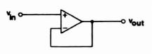
Figure 4.77. Op-amp in unity-gain configuration (Problem 4.13).
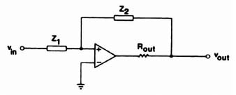
Figure 4.78. Op-amp with nonzero output impedance (Problem 4.15).
4.15. Show that in the circuit of Fig. 4.78, the effective output impedance is Rout(–Ac + 1)/A, where Ac ![]() −Z2/Z1 is the closed-loop gain of the stage. Assume that A
−Z2/Z1 is the closed-loop gain of the stage. Assume that A ![]() 1 and Rout/A
1 and Rout/A ![]() |Z1| and |Z2|.
|Z1| and |Z2|.
4.16. Let the output voltages of the differential op-amp of Fig. 4.50 change by a differential amount so that ![]() and
and ![]() . Show that the sum of the drain currents of Q3 and Q4 remains unchanged. [Hint: Assume that Q3 and Q4 are in their linear regions, and hence you can use Eq. (2.7).]
. Show that the sum of the drain currents of Q3 and Q4 remains unchanged. [Hint: Assume that Q3 and Q4 are in their linear regions, and hence you can use Eq. (2.7).]
4.17. Prove relations (4.107) and (4.108), giving the gain and output impedances, respectively, of the differential op-amp of Fig. 4.50.
4.18. Show that the aspect ratios of the bias circuit of Fig. 4.51 are given by Eq. (4.109) if we choose I = Io/2 in Fig. 4.50, Ibias = Io as the bias chain current, and zero dc common-mode output voltage.
4.19. Show that (if necessary) a differential output op-amp can be constructed from two single-ended-output op-amps using the circuit [15] of Fig. 4.79.
4.20. Show that for the output stage of Fig. 4.65 the maximum sourcing and sinking currents are given by Eqs. (4.119) and (4.120), respectively.
4.21. Find the output impedance of the circuit of Fig. 4.68 (Hint: Set νin = 0 and connect the output terminal to a test source. Calculate the current through the source.)
Figure 4.79. Simplified equivalent circuit of a differential output op-amp (Problem 4.19).
4.22. Prove Eq. (4.121) for the output stage of Fig. 4.70.
4.23. Show that the dominant pole of the compensated op-amp of Fig. 4.71 is given by Eq. (4.124).
4.24. Prove that the common-mode feedback circuit of Fig. 4.71 creates a pole-zero doublet given by Eqs. (4.125) and (4.126).
4.25. Prove Eq. (4.130) for the op-amp of Fig. 4.75.
4.26. Prove that if (1) Aν(s) is a rational function with its poles having negative real parts and (2) Re[kAν(jω)] > − 1 for all ω, the s values satisfying kAν(s) = −1 all have negative real parts. [Hint: By the maximum-modulus theorem of complex functions, if kAν(s) has no poles in the right half of the s plane, its real part in the same region has its minimum value on the jω axis.]
4.27. Show that the input common-mode limit for the differential stage of Fig. 4.36 is given by Eq. (4.80).
4.28. Show that the maximum sourcing and sinking currents for the Fig. 4.65a is given by Eqs. (4.119) and (4.120).
4.29. Show that the dominant pole of the op-amp of Fig. 4.71 is given by Eq. (4.124).
4.30. Prove that the common-mode feedback circuit in the op-amp of Fig. 4.71 creates a pole-zero doublet given by Eqs. (4.125) and (4.126).
REFERENCES
1. D. J. Hamilton and W. G. Howard, Basic Integrated Circuit Engineering, McGraw-Hill, New York, 1975.
2. P. R. Gray and R. G. Meyer, Analysis and Design of Analog Integrated Circuits, Wiley, New York, 1977.
3. K. C. Hsieh, P. R. Gray, D. Senderowicz, and D.G. Messerschmitt, IEEE J. Solid-State Circuits. SC-16 (6), 708–715 (1981).
4. P. R. Gray and R. G. Meyer, MOS operational amplifier design—a tutorial overview, IEEE J. Solid-State Circuits. SC-13 (3), 285–294 (1978).
5. R. J. Widler, IEEE J. Solid-State Circuits. SC-13 (4), 184–191 (1969).
6. R. Gregorian and W. E. Nicholson, Jr., IEEE J. Solid-State Circuits. SC-14 (6), 970–980 (1979).
7. P. R. Gray, Basic MOS operational amplifier design—an overview, in Analog MOS Integrated Circuits: Part II, IEEE Press, New York, 1980.
8. J. H. Huijsing and D. Lineborger, IEEE J. Solid-State Circuits, SC-20 (6), 1144–1150 (1985).
9. P. R. Gray and R. G. Meyer, Analysis and Design of Analog Integrated Circuits, Wiley, New York. 1993.
10. J. E. Solomon, IEEE J. Solid-State Circuits, SC-9 (6). 314–332 (1974).
11. J. C. Bertails, IEEE J. Solid-State Circuits, SC-13 (6), 791–798 (1978).
12. M. Banu, J. M. Khoury, and Y. Tsividis, IEEE J. Solid-State Circuits, SC-23 (6), 1410–1414 (1988).
13. D. Senderowicz, S. F. Dreyer, J. H. Huggins, C. F. Rehim, and C. A. Laber, IEEE J. Solid-State Circuits, SC-17 (6), 1014–1023 (1982).
14. J. N. Babanezhad, IEEE J. Solid-State Circuits, SC-23 (6), 1414–1417 (1988).
15. P. R. Gray and R. G. Meyer, IEEE J. Solid-State Circuits, SC-17 (6), 969–982 (1982).
16. K. C. Hsieh, Proc. Int. Symp. Circuits Syst., pp. 419–422, 1982.
17. D. A. Johns and K. Martin, Analog Integrated Circuit Design, Wiley, New York, 1997.
18. D. Senderowicz, NMOS operational amplifiers, in Design of MOS VLSI Circuits for Telecommunications, Y. Tsividis and P. Antognetti (Eds.), Prentice Hall, Upper Saddle River, N.J., 1985.
19. R. Hogervorst, Design of low-voltage low-power CMOS operational amplifier cells, Ph.D. dissertation. Delft University, 19%.
20. R. Hogervorst, J. P. Tero, R. G. H. Eschauzier, and J. H. Huijsing, IEEE J. Solid-State Circuits, SC-29 (12), 1505–1513 (1994).
21. E. Seevinch, W. de Jager, and P. Buitendijk, IEEE J. Solid-State Circuits, SC-23 (3), 794–801 (1988).
22. R. Castello and P. R. Gray, IEEE J. Solid-State Circuits. SC-20 (6), 1122–1132 (1985).
23. J. N. Babanezhad and R. Gregorian, IEEE J. Solid-State Circuits, SC-22 (6), 1080–1089 (1987).
24. B. K. Ahuja, P. R. Gray, W. M. Baxter, and G. T. Uehara, IEEE J. Solid-State Circuits, SC-19 (6), 892–899 (1984).
25. D. M. Manticelli, IEEE J. Solid-State Circuits, SC-21 (6), 1026–1034 (1986).
26. M. D. Pardoen and M. G. Degrauwe, IEEE J. Solid-State Circuits, SC-25 (2), 501–504 (1990).
27. D. B. Ribner and M. A. Copeland, IEEE J. Solid-State Circuits, SC-19 (6), 919–925 (1984).
*The gain margin is harder to control, and hence much less often used, than the phase margin described next.
*In practice, it is usual 10 choose Cc ≈ CL. This choice satisfies the constraints of Eqs. (4.64) and (4.65) with a large margin.
*The time constant is t0 = 2/(A0 |sp1|) = 2/ω0.
*Such a source indicates that a noise current gmiνni flows in Qi.