
CHAPTER 5
COMPARATORS
Comparators are the second most widely used components in electronic circuits, after operational amplifiers. A voltage comparator is a circuit that compares the instantaneous value of an input signal νin(t) with a reference voltage Vref and produces a logic output level depending on whether the input is larger or smaller than the reference level. The most important application for a high-speed voltage comparator occurs in an analog-to-digital converter system. In fact, the conversion speed is limited by the decision-making response time of the comparator. Other systems may also require voltage comparison, such as zero-crossing detectors, peak detectors, and full-wave rectifiers. In this chapter a number of approaches to comparator design are presented. First, the single-ended auto-zeroing comparator is examined, followed by simple and multistage differential comparators, regenerative comparators, and fully differential comparators. Several design principles are introduced that can be used to minimize input offset voltage and clock-feedthrough effects.
5.1. CIRCUIT MODELING OF A COMPARATOR
One very important and widely used comparator configuration is a high-gain differential input, single-ended output amplifier [1,2], Figure 5.1a shows the symbol of a differential comparator which is very similar to that of an operational amplifier. Usually, the comparator stage is followed by a latch, which is essentially a bistable multivibrator. The latch provides a large and fast output signal whose amplitude and waveform are independent of those of the input signal and is hence well suited for the logic circuits following the latch. If no latch is used, the output νout, should have a large swing, say, 0 to +5 V, as the input changes from −1 mV to + 1 mV. Thus the required gain is around 5 V/2 mV = 2500, or 68 dB. If a latch is used, νout only needs to be higher than the combined offset and threshold voltages of the latch; this value is around 0.2 V or less. Hence a gain of 200 is now adequate. A comparator is therefore essentially a high-gain op-amp designed for open-loop operation. But unlike an op-amp it does not require frequency compensation.

Figure 5.1. (a) Differential-input comparator; (b) transfer curve of ideal comparator.
The transfer curve of the ideal differential comparator is shown in Fig. 5.1b. In this figure the negative input of the comparator in Fig. 5.1a is tied to a reference voltage Vref. When the positive input is greater than Vref the output is high (VOH), and when it is less than Vref, the output is low (VOL). The ideal transfer curve of Fig. 5.1b corresponds to a differential gain of infinity. In actuality the differential gain has a finite value equal to Aν. The dc transfer curve of such a comparator is shown in Fig. 5.2, where ViL and ViH are the input excess voltages called the overdrive. The overdrive is the input level that drive the comparator from some initial saturated input condition to an input level barely in excess of that required to cause the output to switch state. Another nonideal effect of the differential comparator is the input-referred dc offset voltage, Voff. In the absence of the offset voltage (Voff = 0), the comparator dc transfer curve will be symmetrical around Vref. However, for a finite value of Voff, the output will begin changing only after the input difference exceeds Voff. The dc transfer curve of a practical differential comparator with finite gain of Aν and a dc offset voltage of Voff is shown in Fig. 5.3. Finally, the speed or response time is another important parameter of a comparator. In most applications it is required that following an appropriate input level change, the comparator must switch between two output levels with fast rise and fall times in the shortest amount of time. The response time is a function of the input overdrive voltage and it speeds up as the overdrive is increased.

Figure 5.2. Transfer curve of comparator with finite gain.

Figure 5.3. Transfer curve of comparator with finite gain and dc offset voltage.
Another class of comparators, which contain a cascade of inverter stages, is shown in Fig. 5.4. These comparators have a single-ended input/single-ended output configuration and operate in two steps: an auto-zeroing function followed by a comparison cycle. These comparators, which are used primarily in flash analog-to-digital converters, are discussed in the next section.
5.2. SINGLE-ENDED AUTO-ZEROING COMPARATORS [3]
Single-ended auto-zeroing comparators have been used extensively in high-speed flash A/D converters. Considering the system of Fig. 5.4, let the inverters be realized in CMOS technology; then a possible configuration for the input inverters is shown in Fig. 5.5a, with the clock waveforms and node voltage νA illustrated in Fig. 5.5b. The operation is as follows: At t = 0, switches S2 and S3 are closed. S2 connects the left-side terminal of the auto-zeroing capacitor C to ground, while S3 shorts nodes A and B. As a result, the nodes assume a voltage that can be found from the intersection of the input–output dc characteristics of the inverter and the 45° line representing the νA = νB condition. Figure 5.6 illustrates the situation: Fig. 5.6a shows the inverter, and Fig. 5.6b (center curve) illustrates an example of input-output characteristics (with S3 open) for VDD = −VSS = 5 V, and for the threshold voltages, ![]() . The intersection of this curve with the νA = νB line occurs at the origin; this is in the middle of the linear range, where Q1 and Q2 are both in saturation and the gain of the inverter is at maximum. This favorable bias condition is quite insensitive to variations of the threshold voltages, as illustrated by curve 1 (drawn for
. The intersection of this curve with the νA = νB line occurs at the origin; this is in the middle of the linear range, where Q1 and Q2 are both in saturation and the gain of the inverter is at maximum. This favorable bias condition is quite insensitive to variations of the threshold voltages, as illustrated by curve 1 (drawn for ![]() ,
, ![]() ) and curve 2 (for
) and curve 2 (for ![]() = 1.2 V,
= 1.2 V, ![]() −0.7 V); the intersection point is in both cases near the middle of the linear range. (See Problem 5.1 for a graphical identification of the linear range for all three curves.)
−0.7 V); the intersection point is in both cases near the middle of the linear range. (See Problem 5.1 for a graphical identification of the linear range for all three curves.)
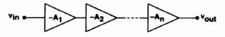
Figure 5.4. Single-ended cascade of inverter stage comparator.

Figure 5.5. Input inverter for a CMOS cascade comparator: (a) circuit diagram; (b) wave-forms.
Returning to the circuit of Fig. 5.5a, clearly during the time interval between t = 0 and t = t1, the capacitor C charges to voltage νAB − 0 = νAB, where νAB is the intersection (self-bias) voltage illustrated in Fig. 5.6b. (There, for nominal threshold voltages, νAB ≈ 0.) Next, at t1, ![]() 3 goes low. This results in nodes A and B being disconnected. Also, part of the charge in the channel of S3 enters C; in addition, through the gate-to-source overlap capacitance of S3, additional clock-feedthrough charges enter C. The dimensions of C and S3 must be determined such that even with the change in νA due to these charges, the Q1–Q2 inverter should remain safely in its linear range. Let the resulting node voltages at A and B be denoted by
3 goes low. This results in nodes A and B being disconnected. Also, part of the charge in the channel of S3 enters C; in addition, through the gate-to-source overlap capacitance of S3, additional clock-feedthrough charges enter C. The dimensions of C and S3 must be determined such that even with the change in νA due to these charges, the Q1–Q2 inverter should remain safely in its linear range. Let the resulting node voltages at A and B be denoted by ![]() and
and ![]() , respectively.
, respectively.

Figure 5.6. Bias conditions for the input inverter: (a) circuit diagram; (b) input–output de characteristics for various threshold voltages (see the text).
Next (at t = t2), S2 opens. Now apart from the small stray capacitance CA, node A is floating and hence νA and νB can drift to any value. However, since C is nearly open circuited at A, there will be only minimal clock feedthrough into C due to the cutoff of S2; also, this clock-feedthrough charge is stored in CA and will be returned to C when S1 closes. Hence this clock feedthrough has no significant effect.
At t = t3, ![]() 1, goes high and C (charged earlier to
1, goes high and C (charged earlier to ![]() during the t1, < t ≤ t2 interval) is connected between the input terminal and node A. Hence the node voltage νA now becomes
during the t1, < t ≤ t2 interval) is connected between the input terminal and node A. Hence the node voltage νA now becomes ![]() , where α = C/(C + CA), and the voltage difference
, where α = C/(C + CA), and the voltage difference ![]() has the same sign as νin. The last statement holds regardless of the values of CA and νAB, the magnitude of the clock feedthrough, and any other parasitic effects. Thus, by monitoring the change
has the same sign as νin. The last statement holds regardless of the values of CA and νAB, the magnitude of the clock feedthrough, and any other parasitic effects. Thus, by monitoring the change ![]() (which is the amplified version of
(which is the amplified version of ![]() ), we can decide whether νin > 0 or νin < 0 holds.
), we can decide whether νin > 0 or νin < 0 holds.
A more complete diagram of a possible circuit is shown schematically in Fig. 5.7a, with the clock signals illustrated in Fig. 5.7b. The operation is as follows. As explained above, by the end of the ![]() 3 pulse, C1 is charged to a voltage
3 pulse, C1 is charged to a voltage ![]() which is suitable for biasing the Q1–Q2 inverter in its linear range. If Q3 is matched to Q1 and Q4 is matched to Q2, the second inverter has the same bias point, and hence is also biased in its linear range. (Note, however, that the clock-feedthrough voltage due to the opening of S3 is amplified by Q1 and Q2 and then connected to the gates of Q3 and Q4; hence the second stage is more vulnerable to this effect). During this time, the Q5–Q6 inverter is also biased in its linear range by S4, and C2 is precharged to the corresponding bias voltage. S4 opens only after S3 does, so that the output voltage νC of the Q5–Q6 inverter is not affected by the amplified clock-feedthrough transient due to S3. It is affected, however, by the opening of S4. This transient can, in turn, be rendered ineffective by C3 and S5. When S5 is closed, the latch is locked in a self-biased balanced state. Thus, when S3 opens, the voltage acquired by C3 would keep a perfectly symmetrical latch in an unstable balanced position. For the latch to function, however, the enabling (“strobe”) signal
which is suitable for biasing the Q1–Q2 inverter in its linear range. If Q3 is matched to Q1 and Q4 is matched to Q2, the second inverter has the same bias point, and hence is also biased in its linear range. (Note, however, that the clock-feedthrough voltage due to the opening of S3 is amplified by Q1 and Q2 and then connected to the gates of Q3 and Q4; hence the second stage is more vulnerable to this effect). During this time, the Q5–Q6 inverter is also biased in its linear range by S4, and C2 is precharged to the corresponding bias voltage. S4 opens only after S3 does, so that the output voltage νC of the Q5–Q6 inverter is not affected by the amplified clock-feedthrough transient due to S3. It is affected, however, by the opening of S4. This transient can, in turn, be rendered ineffective by C3 and S5. When S5 is closed, the latch is locked in a self-biased balanced state. Thus, when S3 opens, the voltage acquired by C3 would keep a perfectly symmetrical latch in an unstable balanced position. For the latch to function, however, the enabling (“strobe”) signal ![]() 6 must also go high.
6 must also go high.
By t = t4, all precharging operations are complete. At this point, S2 is opened and the input node A now floats. When next S1, closes, νD at the input of the latch will rise (if νin < 0) or fall (if νin > 0) from its earlier balanced value. Hence, when ![]() 6 rises, the latch will switch to the appropriate one of its two stable states.
6 rises, the latch will switch to the appropriate one of its two stable states.
Obviously, the system shown in Fig. 5.7 is only one example of the many different possibilities. (It is, in fact, a CMOS equivalent of the circuit described in Ref. 3.) Other circuits may contain only two inverter stages, use source followers as buffers between the various stages, use capacitive coupling also between the first and second stages, and so on. In most cases, however, biasing and auto-zeroing is accomplished using the precharging operations illustrated in Fig. 5.7.
The speed of the cascaded inverter stages is limited by the RC time constants represented by the output resistance Ro of the ith inverter and the input capacitance Cin of the next [i.e., (i + 1)st] inverter. The former is the parallel combination of the drain resistance of the PMOS and NMOS devices in the ith stage; the latter can be approximated by the sum of the Cgd values in the next stage, multiplied by (1 + |Ai + 1) due to the Miller effect. The dc gain A of the inverter is, of course, the sum of the transconductances divided by the sum of the drain conductances of the two devices in the stage. Typical values are Ro ~ 100 kΩ, Cin ~ 1.5 pF, and A ~ 10.

Figure 5.7. CMOS cascade comparator: (a) circuit diagram; (b) clock signals.
5.3. DIFFERENTIAL COMPARATORS
The simplest form of a differential comparator is the uncompensated two-stage transconductance op-amp shown in Fig. 5.8. Although removing the compensation capacitor somewhat speeds up the comparator, the response time is still slow and not adequate for many high-speed applications. As defined earlier, the response time, or propagation delay, is the delay between the time the differential input passes the comparator threshold voltage and the time the output exceeds the input logic level of the subsequent stage. The propagation delay is worst when the input signal changes from a large overdrive level to an opposite level that barely exceeds the threshold voltage. The delay time is determined primarily by the maximum current available to change the parasitic capacitances shown in Fig. 5.8. The capacitance CLA consists of the junction capacitors and the gate-to-source capacitance CGS of transistor Q5. The capacitor CLB is the combination of the junction capacitors and the gate-to-source capacitances of transistors Q3 and Q4. The response time is reduced by minimizing the parasitic capacitances CLA and CLB while increasing the tail current of the differential stage supplied by transistor Q0.
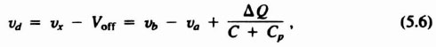
One of the main applications of the CMOS comparator is the switched-capacitor comparator, which is one of the essential blocks of an A/D converter. Figure 5.9a shows the principle of operation of the basic switched-capacitor comparator. During the sample mode, switches S1 and S2 are closed while S3 is open. During the hold and comparison mode, S1 and S2 are open and S3 is closed. In the absence of any nonideal effects, the voltage levels at the end of the hold period are
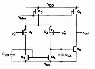
Figure 5.8. Op-amp comparator.

Figure 5.9. (a) Switched-capacitor comparator; (b) switched-capacitor comparator with parasitics.
where Aν is the open-loop voltage gain of the comparator. The circuit of Fig. 5.9a has several nonideal effects. One effect is the dc offset of the comparator, which similar to the CMOS op-amp, is due to the mismatch between the input and load devices of the differential stage. Another source of error is the clock-feedthrough and channel charge-pumping effect of the reset switch S1, which contribute a residual offset charge to the holding capacitor. In Fig. 5.9b the comparator input offset voltage is modeled as the voltage source Voff that is placed in series to one of its inputs. Also shown is the total parasitic capacitance from the inverting input to ground, which is represented by capacitor Cp. Thus for Fig. 5.9b the differential voltage at the input of the comparator at the end of the hold period is

where ΔQ represents the total injected charge on the holding capacitor.

Figure 5.10. Offset-canceled switched-capacitor comparator.
An alternative circuit configuration that can provide offset cancellation is shown in Fig. 5.10. In this figure the reset switch S1 is moved between the comparator inverting input and output. Then, during the sampling phase the capacitor C is charged between the input voltage and the offset of the comparator. In the subsequent hold and comparison phase, as before, switches S1 and S2 are open and S3 is closed, connecting the left side of capacitor C to ground. The voltage at the right side of the capacitor C becomes
which results in the differential voltage at the input of the comparator given by

which is independent of the comparator offset voltage. Although this technique works well for removing the input offset voltage, the clock-feedthrough and channel charge-pumping effects of the reset switch are not eliminated. As Eq. (5.4) shows, the simplest way to reduce the errors due to the charge injection is to increase the size of the sampling capacitor and reduce ΔQ by reducing the size of the reset switch and by using CMOS transmission gate for first-order charge cancellation. Making the size of the holding capacitor large while reducing the size of the reset switch has the adverse effect of increasing the settling time constant of the circuit. For high-speed applications a compromise should be arrived between the sizes of the holding capacitor and the reset switch. An alternative strategy to reduce the clock-feedthrough effect is depicted in Fig. 5.11, where the reset switch is replaced with Q1, a large device, in parallel to Q2 a minimum-size device. At the end of the sample phase, first Q1 turns off while Q2 is still on. The charge injected by Q1 is therefore absorbed by Q2. Subsequently, Q2 turns off and injects some charge to the holding capacitor. The amount of the charge is minimized because the switch has the smallest possible dimensions.

Figure 5.11. Offset-canceled switched-capacitor comparator with reduced clock-feedthrough effects.
The offset-canceling scheme of Fig. 5.10 can be used to sense the difference of two voltages. This is shown in Fig. 5.12, where during the sample phase switches S1 and S2 are closed and the capacitor C is charged between the offset of the comparator and the input voltage νa. During the comparison phase switches S1 and S2 are opened and S3 is closed, connecting the left side of the capacitor to the voltage source νb. Thus, during the comparison phase the voltage at the right side of capacitor C is given by

and the differential voltage at the input of the comparator is
which is, like before, independent of the comparator offset voltage and has a dc offset voltage ΔQ/(C + Cp) due to the residual feedthrough charge.
In this method, since the comparator acts as a unity-gain amplifier during the sample phase, it has to remain stable. A typical circuit is shown in Fig. 5.13. The comparator illustrated is simply a two-stage amplifier with an RC compensating branch Qc − Cc. This branch is effective, however, only during ![]() 1 = 1 half-period, when C is charging through S1 and S2, and hence the comparator functions as an op-amp in a unity-feedback configuration. During
1 = 1 half-period, when C is charging through S1 and S2, and hence the comparator functions as an op-amp in a unity-feedback configuration. During ![]() 2 = 1 interval, the amplifier is in an open-loop configuration, and hence compensation (which slows down its operation) is not needed.
2 = 1 interval, the amplifier is in an open-loop configuration, and hence compensation (which slows down its operation) is not needed.

Figure 5.12. Offset-canceled differential switched-capacitor comparator.
As mentioned before, the offset-canceling comparator still suffers from the dc offset voltage due to the residual feedthrough charge. An effective way for minimizing the errors due to the charge injection effects is the fully differential design scheme, which is discussed later.
In the offset-canceled switched capacitor comparator of Fig. 5.10, when ![]() 1 = 1, capacitor C is charged between the input voltage and the offset of the comparator. At the instant that
1 = 1, capacitor C is charged between the input voltage and the offset of the comparator. At the instant that ![]() 1 goes low, the input signal νin is sampled and held on capacitor C. In the subsequent comparison phase,
1 goes low, the input signal νin is sampled and held on capacitor C. In the subsequent comparison phase, ![]() 2 goes high and the left side of the capacitor is connected to ground, while the right side, in the absence of any offset voltage and clock-feedthrough effect, becomes −νin. This circuit has the important advantage that the input signal is sampled and held during the comparison phase, and the comparator has the full period to determine the polarity of the input signal. One shortcoming of this circuit is that during every offset-canceling phase, while the right side of the capacitor is held at virtual ground, the left side is fully charged to the magnitude of the input signal. As mentioned in an earlier discussion, a large sampling capacitor should be used to minimize the residual offset voltage due to the clock-feedthrough effect. A large sampling capacitor affects the settling time and imposes stringent requirements on the charging capabilities of the input signal source and the comparator output stage. Alternatively, as shown in Fig. 5.14, the phasing of the switches connected to the left side of capacitor C can be interchanged. In this case, during the phase that
2 goes high and the left side of the capacitor is connected to ground, while the right side, in the absence of any offset voltage and clock-feedthrough effect, becomes −νin. This circuit has the important advantage that the input signal is sampled and held during the comparison phase, and the comparator has the full period to determine the polarity of the input signal. One shortcoming of this circuit is that during every offset-canceling phase, while the right side of the capacitor is held at virtual ground, the left side is fully charged to the magnitude of the input signal. As mentioned in an earlier discussion, a large sampling capacitor should be used to minimize the residual offset voltage due to the clock-feedthrough effect. A large sampling capacitor affects the settling time and imposes stringent requirements on the charging capabilities of the input signal source and the comparator output stage. Alternatively, as shown in Fig. 5.14, the phasing of the switches connected to the left side of capacitor C can be interchanged. In this case, during the phase that ![]() 1 is high, the capacitor is charged between the offset of the comparator and ground. In the next phase, when
1 is high, the capacitor is charged between the offset of the comparator and ground. In the next phase, when ![]() 2 goes high, the right side of the capacitor that is connected to the inverting input of the comparator is disconnected from the output, and the left side of the capacitor is connected to the input voltage. At this time, the voltage νx at the inverting input of the comparator is
2 goes high, the right side of the capacitor that is connected to the inverting input of the comparator is disconnected from the output, and the left side of the capacitor is connected to the input voltage. At this time, the voltage νx at the inverting input of the comparator is

Figure 5.13. Op-amp offset-canceled switched-capacitor comparator with compensation capacitor disconnected during the comparison phase.

Figure 5.14. Alternative form of switched-capacitor comparator.

and the voltage across the capacitor is

If C ![]() Cp, νx ≈ νin + Voff, and νc ≈ Voff, the voltage across the capacitor C during
Cp, νx ≈ νin + Voff, and νc ≈ Voff, the voltage across the capacitor C during ![]() 1 and
1 and ![]() 2, remains unchanged at Voff. This greatly relaxes the charging requirements from the input voltage source and is specially suitable for high-speed applications. On the other hand, the disadvantage of this approach is that the sample-and-hold situation no longer exists at the input stage and the comparator inverting input tracks the input signal. For proper operation, the comparator therefore has to make a decision based on the instantaneous value of the input signal.
2, remains unchanged at Voff. This greatly relaxes the charging requirements from the input voltage source and is specially suitable for high-speed applications. On the other hand, the disadvantage of this approach is that the sample-and-hold situation no longer exists at the input stage and the comparator inverting input tracks the input signal. For proper operation, the comparator therefore has to make a decision based on the instantaneous value of the input signal.
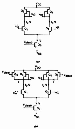
Figure 5.15. (a) Gain block based on source-coupled differential pair with diode-connected load devices; (b) gain-enhanced source-coupled differential pair.
It was mentioned earlier that the response time of the op-amp comparator shown in Fig. 5.8 improves greatly as the input overdrive voltage is increased. A high-resolution high-speed comparator can be realized by using a multistage approach, where several high-speed low-gain differential amplifiers are cascaded followed by a high-gain differential comparator or latch. Figure 5.15a shows a differential amplifier that can be used as the input stage of a comparator. The differential gain of the source coupled pair is given by
where μn and νp are the mobility of the NMOS and PMOS devices. Equation (5.9) shows the dependence of the differential gain on the square root of the device dimensions. Higher-mobility NMOS transistors are used as input devices to achieve higher gain. To increase the gain further, the circuit of Fig. 5.15b can be used where the input transistor transconductance is increased by injecting currents I1 and I2 (I1 = I2) into them from the p-channel current source Q5 and Q6 [4,5]. The gain of the modified circuit is now given by
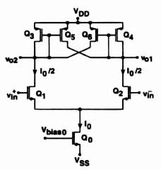
Figure 5.16. Source-coupled differential pair that uses positive feedback to provide increased gain.
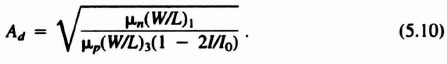
A practical choice is I = 0.9I0/2, which increases the gain by a factor of ![]() .
.
Another method that uses a controlled amount of positive feedback to effectively increase the driver devices transconductance and hence the overall gain is shown in Fig. 5.16 [1]. The gain of the positive feedback gain stage is given by
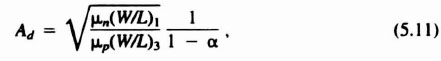
where α = (W/L)5/(W/L)3 is the positive feedback factor that is responsible for increasing the gain. A reasonable value for α is 0.75, which increases the gain by a factor of 4. The value of a is determined by the ratio of the load device dimensions, and although it is a reasonably well controlled parameter, a practical maximum value for a is 0.9, because beyond that any mismatches due to process variations may cause the value of a to approach unity, and per Eq. (5.15), the gain will become infinity and the stage will operate as a cross-coupled latch.
The response times of the gain stages of Figs. 5.15 and 5.16 are limited by the parasitic capacitances of the load devices. The response time of the source coupled differential stage can improve significantly if the diode-connected loads are replaced with simple resistors, as shown in Fig. 5.17. The gain of the resistive load differential stage is given by

Figure 5.17. Resistive-load source-coupled differential pair.
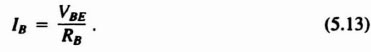
where gmi is the transconductance of the NMOS input devices and RL is the load resistance. One drawback of this circuit is that the voltage drop across the load resistors can vary significantly due to variations in the resistance or the magnitude of the differential stage tail current. The variations of the output common-mode voltage makes it difficult to design multistage amplifiers and bias the circuit to operate under all process variations. One solution to this problem is to use a replica biasing scheme. A schematic of the resistive load differential stage with a simple VBE-based bias generator is shown in Fig. 5.18. The bias current is given by
Assuming that (W/Z)7 = (W/L)6, the voltage drop across the load resistors is given by

This generates a very reproducible fraction of VBE since it is determined by resistor and transistor ratios. In addition to providing known bias voltage, the maximum positive output swing of the differential stage is well controlled at a value of


Figure 5.18. Resistive-load source-coupled differential stage with replica biasing.
Note that to first order the stage output voltage swing is independent of VDD. As an example, if we assume that the bias resistance is RB = 3500 Ω, the bias current is given by
![]()
Using a value of ![]() = 55 μA/V2 for the NMOS transconductance factor and a threshold voltage of VTn = 0.8 V, then for (W/L)l0/(W/L)9 = 2 and (W/L)11/(W/L)12 = 100, the transconductance of the input devices will be
= 55 μA/V2 for the NMOS transconductance factor and a threshold voltage of VTn = 0.8 V, then for (W/L)l0/(W/L)9 = 2 and (W/L)11/(W/L)12 = 100, the transconductance of the input devices will be

For RL = 5000 Ω the differential gain is given by
![]()
and the maximum output voltage swing is, from Eq. (5.15),
![]()
A three-stage direct-coupled comparator circuit comprised of two cascaded resistive load and source-coupled differential stages followed by an op-amp comparator is shown in Fig. 5.19. The overall gain of the first two stages for identical sections is given by
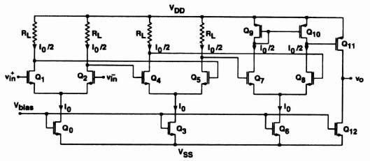
Figure 5.19. Direct-coupled three-stage comparator circuit.
So if each stage has a gain of 10, the overall gain is Ad = 100, and a differential input of 100 μV appears as a 10-mV signal at the input of the final stage. This voltage is large enough to result in a fast response time in the last stage of the comparator. Since the stages are direct coupled, the offset is not canceled. If Voff1, Voff2 and Voff3 represent the offset voltages of the first, second, and third stages, the input referred dc offset voltage is given by
Offset cancellation techniques for the multistage comparators will be introduced later.
5.4. REGENERATIVE COMPARATORS (SCHMITT TRIGGERS)
Often, comparators are used to convert a very slowly varying input signal into an output with abrupt edges, or they are used in a noisy environment to detect an input signal crossing a threshold level. If the response time of the comparator is much faster than the variation of the input signal around the threshold level, the output will chatter around the two stable levels as the input crosses the comparison voltage. Figure 5.20a shows the input signal and the resulting comparator output. In this situation, by employing positive (regenerative) feedback in the circuit, it will exhibit a phenomenon called hysteresis, which will eliminate the chattering effects. The regenerative comparator is commonly referred to as a Schmitt trigger. The response of the comparator with hysteresis to the input signal is shown in Fig. 5.20b.
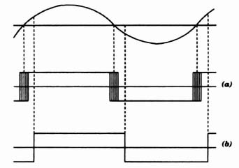
Figure 5.20. Response of a fast comparator to a slowly varying signal in a noisy environment: (a) without hysteresis; (b) with hysteresis.
A Schmitt trigger can be implemented by using positive feedback in a differential comparator, as shown in Fig. 5.21a. Assume that νi < ν1, so that νo = Vo; then ν1s is given by
If νi is now increased, νo remains constant at Vo until νi = ν1. At this triggering voltage, the output regeneratively switches to νo = −Vo and remains at this value as long as νi > ν1. The voltage at the noninverting terminal of the comparator for νi > ν1 is now given by
If we now decrease νi the output remains at νo = −Vo until νi = ν1. At this voltage a regenerative transition takes place and the output returns to Vo almost instantaneously. The complete transfer function is indicated in Fig. 5.21b. Note that because of the hysteresis, the circuit triggers at a higher voltage for increasing than for decreasing signals. Note that Vn < Vp, and the difference between these two values is the hysteresis VH given by

Another method to eliminate the chattering effect around the zero crossing of the input signal is to use the comparator with dynamic hysteresis shown in Fig. 5.22. Assume that νin < ν1, so that νo = +Vo and ν1 = 0. If νin is now increased until νin > 0, the output switches to νo = −Vo. The negative transition of the output will capacitively be coupled to the positive input of the comparator, which also makes a negative transition. This will cause the differential input voltage between the negative and positive inputs of the comparator to become larger and speed up the output transition. Since the first transition at the output of the comparator regeneratively increases the magnitude of the differential input signal, the comparator responds to the first time the input crosses zero and ignores any subsequent zero crossings due to noise. The RC time constant determines the length of the time that the input signal will be ignored after its first zero crossing. If the time constant is made too large, it will limit the maximum frequency that the circuit can operate.
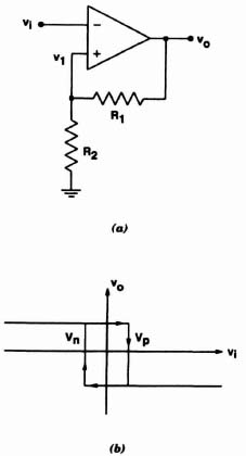
Figure 5.21. (a) Schmitt trigger; (b) composite input–output curve.
Many other ways are available to accomplish hysteresis in a comparator. All of them use some form of positive feedback. Earlier the source-coupled differential pair of Fig. 5.16 was introduced where positive feedback was employed to increase the gain [1]. The gain of the stage is given by Eq. (5.11), where α = (W/L)5/(W/L)3 is the positive feedback factor. For α < 1 [(W/L)5 < (W/L)3], the circuit behaves as a gain stage. For α = 1 the stage becomes a positive feedback latch. For α > 1 the stage becomes a Schmitt trigger circuit with the amount of hysteresis determined by the value of a. Next, the trigger points and amount of hysteresis will be calculated for the case when a > 1.

Figure 5.22. (a) Comparator with dynamic hysteresis; (b) input and output waveforms.
Consider the circuit of Fig. 5.23, where ![]() is connected to ground (or any other reference potential) and the gate of Q2
is connected to ground (or any other reference potential) and the gate of Q2 ![]() is connected to a negative potential much less than zero. Thus Q2 is off and Q1 is on and all the tail current Io flows through Q1 and Q3. The current through transistors Q2, Q4, Q5, and Q6 are zero and the node voltage νo1 is high while νo2 is low. Next assume that the input voltage
is connected to a negative potential much less than zero. Thus Q2 is off and Q1 is on and all the tail current Io flows through Q1 and Q3. The current through transistors Q2, Q4, Q5, and Q6 are zero and the node voltage νo1 is high while νo2 is low. Next assume that the input voltage ![]() is gradually increased so that transistor Q2 begins conducting and part of the tail current Io starts flowing through it. This process continues until the current in transistor Q2 equals the current in Q5. Any increase of the input voltage beyond this point will cause the comparator to switch state so that Q1 turns off and all the tail current flows through Q2. At the switching point assume that the current through transistors Q1 and Q2 are i1, and i2, respectively. Then we have
is gradually increased so that transistor Q2 begins conducting and part of the tail current Io starts flowing through it. This process continues until the current in transistor Q2 equals the current in Q5. Any increase of the input voltage beyond this point will cause the comparator to switch state so that Q1 turns off and all the tail current flows through Q2. At the switching point assume that the current through transistors Q1 and Q2 are i1, and i2, respectively. Then we have
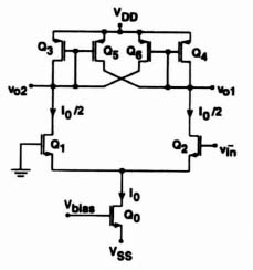
Figure 5.23. Source-coupled differential pair with positive feedback factor α > 1 for hysteresis.
or

Now the gate-to-source (νGS) voltages of Q1 and Q2 can be calculated from their respective drain currents and are given by
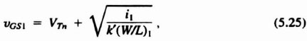

In the equations above, i2 > i1, so νGS2 > νGS1 and since the gate of Q1 is tied to ground, the difference between νGS2 and νGS1 is the positive trigger level, equal to

Using Eqs. (5.23) and (5.24) and since (W/L)1 = (W/L)2, Eq. (5.27) will be simplified to

When the input voltage is increased beyond Vtrig+, the comparator switches and νo1 turns low and νo2s goes high. Now transistor Q2 is on and Q1 is off, and all the tail current Io flows through Q2 and Q4. The currents in transistors Q1, Q3, Q5, and Q6 are zero.
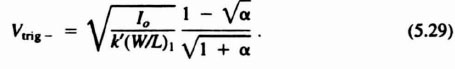
Next consider reducing the input voltage ![]() , so that the current in Q2 starts decreasing and Q1 starts conducting. A similar argument can prove that the negative trigger point occurs when i1 = i6. It can be shown that the negative trigger point
, so that the current in Q2 starts decreasing and Q1 starts conducting. A similar argument can prove that the negative trigger point occurs when i1 = i6. It can be shown that the negative trigger point ![]() is given by
is given by
The hysteresis can be calculated as
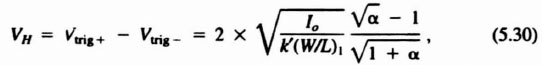
where α = [(W/L)5/(W/L)3] = [(W/L)6/(W/L)4].
The complete schematic of a comparator with hysteresis, which consists of a source-coupled differential pair with positive feedback, and a differential-to-single-ended converter is shown in Fig. 5.24. For this circuit the value of α = [(W/L)5/(W/L)3] = [(W/L)6/(W/L)4] is greater than 1 and the hysteresis is given by Eq. 5.30.

Figure 5.24. Complete schematic of a comparator with hysteresis.

Figure 5.25. Fully differential input offset storage (IOS) comparator.
5.5. FULLY DIFFERENTIAL COMPARATORS
For high-accuracy applications an effective way for reducing the dc offset voltage due to the feedthrough charge is to use a fully differential scheme for the comparators. In such circuits, not only are clock-feedthrough effects reduced, but power supply noise and 1/f noise also tend to cancel. An offset-canceling fully differential comparator is shown in Fig. 5.25. In this scheme, during the offset cancellation mode, switches S0 to S3 are on while switches S4 and S5 are off. This will cause a unity-gain feedback loop to be established around the comparator and the two sampling capacitors to be charged between ground and the offset voltage of the comparator. During the tracking mode, switches S0 to S3 turn off, breaking the feedback loop of the comparator; S4 and S5 turn on and connect the capacitors to the input signal. The input differential voltage is amplified by the comparator and is sensed by the latch, which provides a logic level at its output, representing the polarity of the input differential voltage. If VoffA and VoffL represent the input offset voltages of the comparator and the latch, Q0 and Q1, represent the feedthrough charges of switches S0 and S1, the residual input referred offset voltage is given by
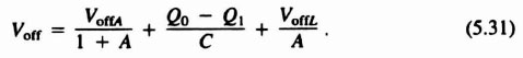
From Eq. (5.31), if the charges injected by switches S0 and S1 match while the common-mode voltage will be slightly affected by an amount equal to (Q0 + Q1)2C, the differential input voltage, ΔQ/C = (Q0 − Q1)/C will be zero. In practice, the charge injected by the two switches will never match, but the residual offset voltage due to the mismatches in the clock feedthrough will be an order of magnitude less than in the single-ended case. For this reason most advanced integrated comparators use fully differential design technique.
The offset compensation technique shown in Fig. 5.25 is known as the input offset storage (IOS) topology [4,5]. It is characterized by closing a unity-gain feed-back loop around the comparator and storing the resulting offset voltage on the input capacitors. In this configuration, since the input signal is capacitively coupled, it has a wide input dynamic range. Also, since during the cancellation phase, the comparator is connected as a unity-gain amplifier, it recovers from the input overdrive as well as starting the tracking phase in its active region, thereby improving its response time. The disadvantage of this topology is evident from Eq. (5.31), where it can be seen that to reduce the residual input offset voltage, the comparator should have a high gain and a large value input capacitor should be used. A comparator with high gain consumes more power and is harder to compensate for stable operation during the offset cancellation phase. A large sampling capacitor increases the settling time and hence degrades the response time of the comparator. It also loads the preceding circuit and causes a large amount of transient noise.

Figure 5.26. Fully differential offset canceling comparator.
Figure 5.26 shows a simple fully differential stage employing the input offset storage topology [6, pp. 99–102]. In this circuit the two auto-zeroing capacitors C1 and C2 are precharged during the ![]() 1 interval between ground and νs where νs is the self-biased input voltage of the amplifier. When
1 interval between ground and νs where νs is the self-biased input voltage of the amplifier. When ![]() 2 goes high, the input voltage νin is sensed by the comparator and an amplified differential voltage
2 goes high, the input voltage νin is sensed by the comparator and an amplified differential voltage ![]() appears at the output. There is also a clock-feedthrough signal at each input node, which appears as a common-mode signal and is hence suppressed. A high-gain (>80 dB) comparator, using a folded-ease ode first stage followed by a case ode second stage with a switched compensation capacitor is described in Ref. 7.
appears at the output. There is also a clock-feedthrough signal at each input node, which appears as a common-mode signal and is hence suppressed. A high-gain (>80 dB) comparator, using a folded-ease ode first stage followed by a case ode second stage with a switched compensation capacitor is described in Ref. 7.
In high-resolution applications a single-stage high-gain offset-canceling comparator such as the one shown in Fig. 5.26 will have a long response time. Therefore, high-resolution comparators use a multistage design. Each stage of the multistage design uses one of the low-gain amplifier stages shown in Figs. 5.15 to 5.17. A three-stage fully differential input offset storage (IOS) multistage comparator and the individual gain stage are shown in Fig. 5.27a and b, respectively [8], The gain stage is similar to the gain-enhanced amplifier stage described earlier and shown in Fig. 5.15b. The two cascode transistors Q7 and Q8 have been added to reduce the Miller capacitance at the input. To recover from overdrive voltage and speed up the settling time, the reset switch Q9 is used to equalize the differential output of the gain stage for a short period during the offset storage cycle. Each stage is capacitively coupled to the next one, and by closing the feedback loop around each stage independently, the possible instability problem of a three-stage amplifier with one feedback loop around all three stages is eliminated. The circuit operates as follows. During the offset storage mode, the feedback switches are closed, a unity-gain feedback loop is established around each gain stage, and the offset of the comparators is stored on the input capacitors. In the tracking mode the feedback around the comparators is opened and the input differential voltage is sensed and amplified by A3, where A is the voltage gain of each amplifier stage. The output of the comparator is strobed by a latch that produces a logic level at its output. The mismatch between the channel charge injected from the feedback switches introduces an uncanceled offset at the input of each gain stage. The total input-referred dc offset voltage is dominated by the offset of the first stage. It is possible to reduce this type of error by implementing the sequential clocking scheme shown in Fig. 5.27c, where the gain stages are brought out of the offset cancellation mode sequentially, A0 first and A2 last [1,8]. When switches S1 and S2 are opened, A0 leaves the offset cancellation mode while A1 and A2 remain in that mode. The offset voltages due to the charge injection mismatches of S1 and S2 on capacitors C1 and C2 are amplified by the first stage and stored on capacitors C3 and C4 before the other feedback switches are opened. This can be repeated with switches S3 and S4 opening before S5 and S6 switches to cancel its charge injection error. To ensure proper operation, the delay between the clock edges shown in Fig. 5.27c should be long enough to allow the input capacitors of the next stage to fully absorb the offset voltage of the previous stage.
An alternative offset cancellation technique is shown in Fig. 5.28 [4]. In this method the offset is canceled by shorting the preamplifier inputs and storing the amplifier offset on the output coupling capacitors. This topology, known as output offset storage (OOS), operates as follows. During offset cancellation, switches S0 to S3 are on, switches S4 and S5 are off, and the output of the gain stage is AVoffa, where A is the gain of the amplifier. In this phase the amplified offset of the gain stage is stored on C1 and C2. During the tracking mode, S1 to S4 are off, S5 and S6 are on, and the amplifier senses and amplifies the analog differential voltage. This voltage is subsequently sensed and amplified by a latch which provides a logic level at its output. In this comparator employing OOS, the residual offset is
where VOFFL is the latch offset and ΔQ = Q0 − Q1 is mismatch in charge injection from switches S0 and S1 onto capacitors C1 and C2. As suggested by Eq. (5.32), the offset of the amplifier is canceled completely. This is evident from Fig. 5.28, where during the cancellation mode the inputs of the amplifier and the latch are both zero; hence a zero difference of the comparator input gives a zero difference at the latch input. Also, as shown in Eq. (5.32), the offset due to the charge injection of the switches is divided by the gain of the amplifier, resulting in a smaller overall input-referred offset voltage compared to that of IOS, as evident from Eq. (5.31).
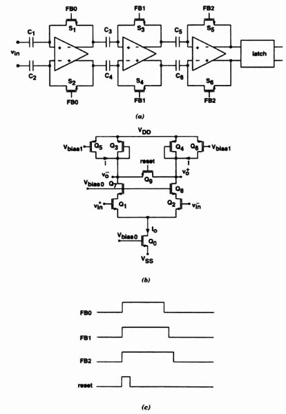
Figure 5.27. (a) Three-stage IOS comparator; (b) gain-enhanced amplifier stage; (c) sequential clocking scheme.

Figure 5.28. Fully differential output offset storage (OOS) comparator.
In addition to having a lower residual dc offset voltage, the OOS topology generally has a smaller input capacitance, which is limited to the input capacitance of the amplifier, which can be maintained well below 100fF. The OOS topology is therefore the preferred choice in applications where a low input capacitance is required, such as a flash A/D converter, where many comparators are connected in parallel. One drawback of the OOS topology is its limited-input common-mode range, which is due to the dc coupling at its input. Another drawback is that during offset cancellation mode, the amplifier in an OOS operates in open-loop mode and the input offset is amplified by its gain. Therefore, a low-gain amplifier should be used to ensure operations in the active region under maximum input dc offset voltage.
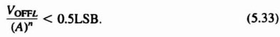
Typically, the comparator is followed by a standard CMOS latch with a potentially large dc offset voltage. Therefore, to achieve a low input-referred offset voltage, as suggested by Eq. (5.32), a high-gain amplifier should be used. Consequently, in high-resolution applications, the use of a single-stage comparator is not feasible, and similar to the IOS topology, a multistage calibration technique will be required. Figure 5.29a illustrates a three-stage OOS comparator where each stage can be constructed from one of the low-gain amplifier stages shown in Figs. 5.15 to 5.17. A sequential clocking scheme such as the one shown in Fig. 5.29b will then reduce the dc offset due to the clock feedthrough. If VOFFL represents the offset of the latch, the number of amplifier stages n, and the corresponding gain A, should be selected such that the input-referred offset voltage is less than 0.5LSB, or
After the value of the required gain (A)n is determined, the number of the stages is selected to provide the smallest delay [8].

Figure 5.29. (a) Three-stage OOS comparator; (b) sequential clocking scheme.
The multistage calibration technique is an effective method to reduce the contribution of the latch offset to the overall residual input-referred dc offset voltage. An alternative method to improve the performance of a fully differential comparator is to apply the offset cancellation to both the gain stage and the latch [4], By canceling the offset of the latch, it will not be necessary to use multistage low-gain amplifiers, and high performance can be achieved by using a single low-gain amplifier that is optimized for both speed and power dissipation.
The simplified block diagram of a CMOS comparator that applies offset cancellation to both the amplifier and the latch is shown in Fig. 3.30. It consists of two transconductance amplifiers, Gm1 and Gm2, that share the same output nodes, load resistors, and offset storage capacitors. In this circuit B1 and B2 are buffers that isolate the common output nodes from the feedback capacitors. The operation of the circuit is as follows. During the offset cancellation mode, S1 to S6 are on, S7 to S10 are off, the inputs of Gm1 and Gm2 are grounded, and their offsets are amplified and stored on capacitors C1 and C2. During the comparison mode, S1 to S6 turn off, S7 to S10 turn on, the capacitors are connected in the feedback loop of Gm2, the inputs of Gm1 are released from ground, and the input voltage is sensed. The input voltage is amplified by Gm1 to establish an imbalance in output nodes A and B which is coupled to the inputs of Gm2 through C1 and C2, initiating regeneration around Gm2. This calibration method can be viewed as an output offset storage applied to both the amplifier Gm1 and the latch Gm2, resulting in complete cancellation of their offsets.
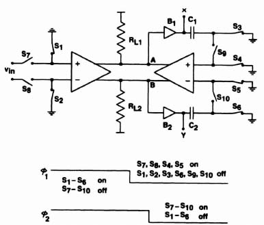
Figure 5.30. CMOS comparator block diagram and timing.
A CMOS comparator based on the topology of Fig. 5.30 is shown in Fig. 5.31. In this circuit the source-coupled pairs Q1–Q2 and Q3–Q4 constitute amplifiers Gm1 and Gm2 respectively. The loads are formed from the diode-connected transistors Q5 and Q6 and gain enhancement devices Q7 and Q8. The output common-mode voltage is set by transistors Q5 and Q6. The source followers Q9 and Q10 serve as buffers B1 and B2 in Fig. 5.30. As described earlier and shown in Fig. 5.15a, the additional current sources, Q7 and Q8, increase the gain and decrease the voltage drop across Q5 and Q6. Normally, the gates of Q7 and Q8 would be connected to a fixed bias voltage. However, by connecting the gates to the inputs of the differential stage, the push-pull operation of Q3 with Q7 and Q4 with Q8 improves the charge and discharge response times of nodes A and B in the following way: When, for example, node F goes low and node E goes high, the current in Q8 is increased, thereby pulling node B more quickly to a higher voltage. The current in Q7 is reduced, thus allowing Q3 to discharge node A to a lower voltage much faster.
In this circuit, during the calibration mode, S1 to S6 are on, S7 to S10 are off, and the combined offset voltages of Gm1 and Gm2 are stored on capacitors C1 and C2. During the comparison mode the comparators are connected in the feedback loops of Gm2 and the input voltage is sensed by Gm1. Any differential input voltage will off-balance the currents of the differential pair Q1–Q2, which reflects into a differential voltage at nodes A and B. This voltage is regeneratively coupled to the inputs of Gm2 through capacitors C1 and C2, causing the outputs to switch. Since the comparator of Fig. 5.31 includes calibration of both the amplifier and the latch, its residual offset is due primarily to mismatches in the charge injection of switches S3 to S6, S9, and S10.
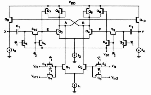
Figure 5.31. CMOS comparator circuit diagram.
The differential output voltage swing of the comparator is normally on the order of 1 to 2 V. The comparator can be followed by a latch or a nonregenerative amplifier such as the one shown in Fig. 5.32 to develop full CMOS levels from the differential output. The bias circuit consisting of transistor Q15–Q17 and current source I1 replicates the X and Y common-mode voltage at the source of Q17 and generate pull-up currents in Q13 and Q14 that, during reset, are equal to pull-down currents in Q11 and Q12 if their gates are driven from X and Y.
5.6. LATCHES
As mentioned earlier, to provide the gain needed to generate logic levels at the output, as well as synchronize the operation of the comparator with other parts of a system, the amplifier of the comparator is usually followed by a latch. The latter can simply be a cross-coupled bistable multivibrator. Some possible latch circuits are shown in Figs. 5.33 to 5.35. The circuit of Fig. 5.33 is a dynamic CMOS latch [9] used to amplify small differences to CMOS levels. In this circuit, when ![]() is low, Q5 is off, S1 and S2 are on, and the input capacitances are precharged to νin1 and νin2. Subsequently, when
is low, Q5 is off, S1 and S2 are on, and the input capacitances are precharged to νin1 and νin2. Subsequently, when ![]() goes high it turns off S1 and S2 to isolate nodes X and Y from the input terminals and turns on Q5 to initiate regeneration, and the latch assumes one of its stable states, depending on the sign of νin1 − νin2.
goes high it turns off S1 and S2 to isolate nodes X and Y from the input terminals and turns on Q5 to initiate regeneration, and the latch assumes one of its stable states, depending on the sign of νin1 − νin2.
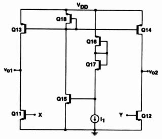
Figure 5.32. CMOS comparator output stage.
The latch of Fig. 5.34 also includes self-biasing and auto-zeroing circuitry [6, pp. 99–102]. The operation is as follows. When ![]() 2 goes high, S4 and S5 short circuit the gates and drains of Q2 and Q3, respectively. This action biases the two inverters Q2–Q6 and Q3–Q6 (which form the multivibrator) in their linear regions. It also precharges the capacitors C3 and C4 such that any asymmetry between the two inverters is compensated for by the slightly different bias voltages provided by C3 and C4. During this time the multivibrator has a loop gain less than 1, and hence it does not switch into either one of its stable states. Next, when
2 goes high, S4 and S5 short circuit the gates and drains of Q2 and Q3, respectively. This action biases the two inverters Q2–Q6 and Q3–Q6 (which form the multivibrator) in their linear regions. It also precharges the capacitors C3 and C4 such that any asymmetry between the two inverters is compensated for by the slightly different bias voltages provided by C3 and C4. During this time the multivibrator has a loop gain less than 1, and hence it does not switch into either one of its stable states. Next, when ![]() 1 and
1 and ![]() 3 go high, S2 and S3 precharge C1 to
3 go high, S2 and S3 precharge C1 to ![]() , while S6 and S7 precharge C2 to
, while S6 and S7 precharge C2 to ![]() . Next,
. Next, ![]() 1 goes low and the input devices Q1 and Q4 are released from their self-biased states, leaving C1 and C2 floating. Then
1 goes low and the input devices Q1 and Q4 are released from their self-biased states, leaving C1 and C2 floating. Then ![]() 3 goes low and
3 goes low and ![]() high; νA now changes by
high; νA now changes by ![]() , while νB changes by
, while νB changes by ![]() from the self-biased values. This also causes corresponding changes in νC and νD inside the multivibrator. When
from the self-biased values. This also causes corresponding changes in νC and νD inside the multivibrator. When ![]() 2 finally goes low, unleashing the multivibrator, the voltage differences between νA and νB as well as νC and νD cause it to go to the appropriate stable state; νC will be high and νD low if
2 finally goes low, unleashing the multivibrator, the voltage differences between νA and νB as well as νC and νD cause it to go to the appropriate stable state; νC will be high and νD low if ![]() holds, or νC low and νD high if
holds, or νC low and νD high if ![]() is valid.
is valid.
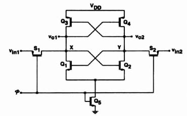
Figure 5.33. Dynamic CMOS latch.
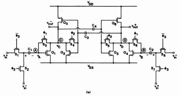
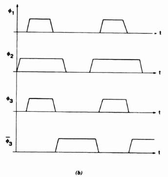
Figure 5.34. Capacitively coupled latch with auto-zeroing input circuitry: (a) circuit diagram; (b) clock signals.
The sequence in which the various clock phases rise and fall is important for proper operation of this latch circuit (as it is for almost any other). The reader is urged to analyze the operation if (say) ![]() 2 goes low before
2 goes low before ![]() 3 goes high, and so on, to convince himself or herself of the validity of this statement.
3 goes high, and so on, to convince himself or herself of the validity of this statement.
Yet another latch [10] is shown in Fig. 5.35. In this circuit, transistors Q1, Q2, Q3, Q4 and Q7 act as a differential preamplifier when S5 is closed. On the other hand, when S6 is closed, Q3, Q4, Q5, Q6, and Q7, form a bistable multivibrator. When ![]() 1,
1, ![]() 2, and
2, and ![]() 3 are high, the preamplifier is self-biased and C1 and C2 are precharged to
3 are high, the preamplifier is self-biased and C1 and C2 are precharged to ![]() and
and ![]() , respectively. Then
, respectively. Then ![]() 1 goes low, allowing the amplifier to function and leaving C1 and C2 floating at nodes A and B. Next, the bottom terminals of C1 and C2 are switched to
1 goes low, allowing the amplifier to function and leaving C1 and C2 floating at nodes A and B. Next, the bottom terminals of C1 and C2 are switched to ![]() and
and ![]() , respectively; this causes an amplified voltage difference between nodes C and D. At this point, S5 slowly opens and S6 slowly closes. This causes the multivibrator to come to life and to assume one of its stable states. The state chosen is determined by the sign of νC − νD.
, respectively; this causes an amplified voltage difference between nodes C and D. At this point, S5 slowly opens and S6 slowly closes. This causes the multivibrator to come to life and to assume one of its stable states. The state chosen is determined by the sign of νC − νD.

Figure 5.35. Preamplifier-latch combination: (a) circuit diagram; (b) clock signals.
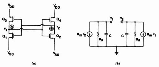
Figure 5.36. Direct-coupled multivibrator: (a) circuit diagram; (b) small-signal equivalent circuit.
Even if the amplifier and the latch are built from the same types of inverters, the rise and fall times of the amplifier will be much longer than those of the latch. To understand this phenomenon, consider the simple multivibrator of Fig. 5.36a. Its small-signal equivalent circuit with all devices in the saturation region is shown in Fig. 5.36b, where gm = gm1 + gm3 = gm2 + gm4 and gd = gd1 + gd3 = gd2 + gd4; also, C is the capacitance loading nodes A and B. It can easily be shown (Problem 5.12) that the natural modes (poles) of the circuit of Fig. 5.36 are s1,2 = ±gm/C. Hence its transients are exponential functions with a time constant τ = C/gm. In the absence of positive feedback, if the inverters Q1–Q3 and Q2–Q4 are simply cascaded as in an amplifier, the time constant is τ′ = C/gd. The ratio of the time constants is τ/τ′ = gd/gm = 1/A, where A is the gain of the inverter [11], Since typically, A = 10, the latch can be about an order of magnitude faster than the amplifier driving it. It is possible to take advantage of the speed of the latch by using two amplifiers to feed a single latch (Fig. 5.37a). In this system [12], the two amplifiers have the same configuration as the two input stages in the circuit of Fig. 5.7a. They alternate in auto-zeroing and amplifying, but the amplifying periods have a duty cycle longer than 50% (Fig. 5.37b), so that the input of the latch can receive a continuous-time input signal. To assure this, the intervals during which the switches SA and SB connect the amplifiers to the latch overlap. Thus the latch clock frequency (which is the effective overall clock frequency of the comparator) can be different from the amplifier clock rates. This system can thus operate about 10 times faster than the usual single-amplifier version, since the limiting factor is now the speed of the latch, not that of the amplifier.

Figure 5.37. Fast comparator system with two amplifiers and a single latch: (a) circuit diagram; (b) clock signals.
Figure 5.38. Reduction of input offset voltage by capacitive storage for a multistage comparator (for Problem 5.5).
PROBLEMS
5.1. For the inverter of Fig. 5.6a with the input–output characteristics shown in Fig. 5.6b, prove that the limits of the linear range (where Q1 and Q2 are both in saturation) are the intersections of the characteristics with the 45° lines νB = νA + ![]() and νB = νA − VTn. Draw these lines for the curves of Fig. 5.6b, and identify the linear ranges.
and νB = νA − VTn. Draw these lines for the curves of Fig. 5.6b, and identify the linear ranges.
5.2. The circuit of Fig. 5.7a is to be fabricated using a CMOS process with the following parameters: ![]() , tox = 800 A, λn = 0.012 V−1, and λp = 0.02 V−1. Design the input inverter such that for νA = 0 V, νB = 0 V and iD1 = iD2 = 50 μA. How much is the gain of the stage? (Hint: Use the formulas of Tables 2.2 and 2.3.)
, tox = 800 A, λn = 0.012 V−1, and λp = 0.02 V−1. Design the input inverter such that for νA = 0 V, νB = 0 V and iD1 = iD2 = 50 μA. How much is the gain of the stage? (Hint: Use the formulas of Tables 2.2 and 2.3.)
5.3. In the circuit of Fig. 5.7a, the clock-feedthrough capacitance between the gate of S3 and node A is 15fF. The clock voltage is 10 V peak to peak. How large must C1 be if the first two inverters (Q1–Q2 and Q3–Q4) are to operate with all devices in saturation, despite the clock-feedthrough voltage at node A? Assume the W and L values obtained in Problem 5.2 for the two input inverters.
5.4. Show that the differential voltage at the input of the comparator of Fig. 5.9b at the end of the hold period is given by Eq. (5.2).
5.5. Calculate the effective input offset voltage of the auto-zeroed comparator of Fig. 5.38 from the individual gains and offset voltages of its two stages A1 and A2. Assume that the clock-feedthrough charge is ΔQ and the input capacitance of the first stage is Cp.
5.6. Prove Eq. (5.10) for the comparator of Fig. 5.15b.
5.7. For the source-coupled differential stage of Fig. 5.18, determine the values of RB and RL, the aspect ratios of Q6–Q7 and Q9–Q10 and the dimensions of Q11 and Q12 such that the differential gain becomes 16. (Assume that k′n = 55 mA/V2 and VTn = 0.8 V.)
5.8. Prove Eq. (5.17) for the three-stage comparator circuit of Fig. 5.19.
5.9. Select values for R1, and R2 so that the comparator of Fig. 5.21a has ±30 mV hysteresis. (Assume that VDD = 5 V and VSS = −5 V.)
5.10. For the circuit of Fig. 5.24, if W1 = W2 = 50 μm, L1 = L2 = 2 μm, and the tail current I0 = 100 μA, calculate a from Eqs. (5.28) and (5.29) such that ![]() = 30 mV.
= 30 mV.
5.11. Prove Eq. (5.31) for the circuit of Fig. 5.25.
5.12. For the multivibrator of Fig. 5.36a: (a) derive the small-signal equivalent circuit of Fig. 5.36b; (b) using Laplace transform analysis, find the natural modes of the circuit; and (c) find the natural modes for the case when the two inverters (Q1–Q3 and Q2–Q4) are cascaded without closed-loop feedback, (d) What conclusions can be drawn from the relative magnitudes of the natural modes of the two circuits?
REFERENCES
1. D. J. Allstot, IEEE J. Solid-State Circuits. SC-17(6), 1080–1087 (1982).
2. R. Gregorian and J. G. Gord, IEEE J. Solid-State Circuits, SC-17(6), 698–700 (1983).
3. Y. S. Lee, L. M. Tennan, and L. G. Heller, IEEE J. Solid-State Circuits, SC-13(2), 294–297 (1978).
4. B. Razavi and B. A. Wooley, IEEE J. Solid-State Circuits, SC-27(6), 1916–1926 (1992).
5. B. Razavi, Principles of Data Conversion System Design, IEEE Press, New York, 1995.
6. K. W. Martin, Project Reports, Microelectronics Innovation and Computer Research Opportunities (MICRO) Program, University of California, Berkeley, Calif., 1983.
7. H. S. Lee, D. A. Hodges, and P. R. Gray, IEEE Int. Solid-State Circuits Conf., pp. 64–65, 1984.
8. J. Doemberg, P. R. Gray, and D. A. Hodges, IEEE J. Solid-State Circuits, SC-24(2), 241–249 (1989).
9. S. Chin, M. K. Mayes, and R. Filippi, ISSCC Dig. Tech. Pap., pp. 16–17, Feb. 1989.
10. K. Martin, personal communication.
11. W. C. Black, Jr., personal communication.
12. Y. Fujita, E. Masuda, S. Sakamoto, T. Sakane, and Y. Sato, IEEE Int. Solid-State Circuits Conf., pp. 56–57, Feb. 1984.