
CHAPTER 3
BASIC ANALOG CMOS SUBCIRCUITS
In this chapter some of the basic subcircuits commonly utilized in analog MOS integrated circuits are examined. These blocks include a variety of bias circuits, current mirrors, single-stage amplifiers, source followers, and differential stages. These subcircuits are typically combined to synthesize a more complex circuit function. The operational amplifier and comparator, covered in later chapters, are examples of how simple subcircuits are combined to form more complex functions.
The first part of this chapter covers the subject of the bias circuits in CMOS technology and the current mirrors. Next, the CMOS gain stage is introduced, with particular emphasis on the use of active devices as active loads. The current mirror subcircuit covered as a biasing element is utilized as a dynamic load to obtain very high voltage gains from a single-stage amplifier. The differential amplifier, which represents a broad class of circuits, is discussed next. The differential amplifier is one of the most widely used gain stages, whose basic function is to amplify the difference between two input signals. Finally, the last part of the chapter deals with the small-signal analysis and frequency response of CMOS amplifier stages. A good understanding of the topics presented in this chapter is essential for the analog CMOS designer, as most designs start at the subcircuit level and progress upward to realize a more complex function.
3.1. BIAS CIRCUITS IN MOS TECHNOLOGY
Op-amp and amplifier stages, described in detail later, need various dc bias voltages and currents for their operation. An ideal voltage or current bias is independent of the dc power supply voltages (VDD > 0 and VSS ≤ 0) and of temperature.
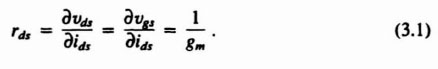
To obtain the dc bias voltages Vo1, Vo2, …, Von, where VSS < Vo1 < Vo2 < … Von < VDD, voltage division can be used. Pure resistive dividers are seldom used in MOS technology because the resulting voltages cannot be used directly to establish bias currents in MOS transistors. Instead, combinations of MOSFETs and resistors are often used. A MOS transistor with its gate connected to the drain forms a two- terminal device, as shown in Fig. 3.1a. Its current–voltage characteristics are shown in Fig. 3.1b. Since VDS = VGS the dynamic resistance rds is characterized by

Figure 3.1. (a) Diode-connected NMOS transistor; (b) current–voltage characteristic of diode-connected transistor.
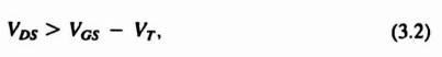
Therefore, a useful approximation valid for low frequencies, small signals, and negligible substrate effects is that the device behaves like a resistor of value 1/gm. Any number of n- and p-channel devices and resistors can be combined to form a voltage divider, as shown in Fig. 3.2, where both n- and p-channel transistors are used and VSS = 0 is chosen. Since VGS = VDS here for both devices, the condition for saturation,

Figure 3.2. Voltage-divider-based bias circuit.
is satisfied. Hence the common value of the drain currents is given approximately by

Here Ibias is usually specified; then Vo1 and Vo2 can be selected and Eq. (3.3) used to find the W/L ratios of the devices and the value R of the resistor.
An undesirable feature of this configuration is that the bias voltages and current depend on the supply voltages VDD and VSS. In fact, the bias current increases rapidly with increasing power supply voltage. Since such bias strings are used to provide bias for other devices in the circuit, the dc power consumption of the overall circuit becomes heavily dependent on the supply voltages.
A CMOS circuit with (theoretically) perfect supply independence is shown in Fig. 3.3. If Q3 and Q4 are matched transistors so that (W/L)3 = (W/L)4, they ideally carry equal currents. Choosing (W/L)1 = (W/L)2 will then result in VGS1 = VGS2, and the voltage across the resistor, IbiasR, will be equal to VGS0. This equilibrium condition leads to the equation

Figure 3.3. VT-referenced supply-independent CMOS bias source.
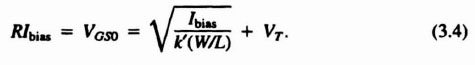
Equation (3.4), which is independent of VDD, can be solved to obtain Ibias. Note that in this analysis we neglected the effects of channel-length modulation (i.e., we assumed that ID is independent of VDS).
An alternative version of the bias circuit shown in Fig. 3.3 that uses the base–emitter voltage (VBE) of a bipolar transistor as the reference voltage is shown in Fig. 3.4a. In a CMOS process, the substrate, well, and the source–drain junction inside the well can be used to form a vertical bipolar transistor. For example. Fig. 3.4b shows a vertical pnp device that is formed in an n-well process. The collector of this pnp device is the p− substrate that is permanently connected to the most negative voltage on the chip. For the bipolar transistor, the collector current is given by

Figure 3.4. (a) VBE-basecl supply-independent bias circuit; (b) vertical pnp bipolar transistor in an n-well CMOS process.
where VBE is the base–emitter voltage, VT = kT/q, and Is is a constant current, which is proportional to the cross-sectional area of the emitter, which is used to describe the transfer characteristic of the transistor in the forward active region.
In Fig. 3.4a, as in Fig. 3.3, if (W/L)1 = (W/L)2 and (W/L)3 = (W/L)4, equal currents are forced through the two branches of the bias circuit and the voltage drop across resistor R equals VBE. Thus the bias current is given by

Combining Eqs. (3.5) and (3.6), we have
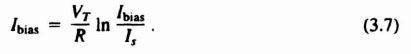
This equation can be solved iteratively for Ibias.
Both supply-independent bias circuits have a second trivial steady-state condition, cutoff when Ibias = 0. To prevent the bias circuit from settling to the wrong steady- state condition, a startup circuit is necessary in all practical applications. The circuit to the right of the dashed line in Fig. 3.5 functions as a startup circuit. If Ibias = 0, Q5 is off and the voltage at node A is high, causing Q6 to turn on and draw a current through Q3, forcing the circuit to move to its other equilibrium state. Once the circuit settles in the desired state, Q5 turns on and node A goes low, turning off Q6. At this state the startup circuit is essentially out of the picture.

Figure 3.5. Supply-independent bias circuit with startup.
Another important performance aspect of the bias circuits is their temperature dependence. Unfortunately, supply-independent bias circuits are not necessarily temperature independent, because the base–emitter voltage (VBE), and gate-to-source voltage (VGS) are both temperature dependent. If the temperature coefficient TCF is defined as the relative change of the bias current per degree Celsius temperature variation, we have [1]

Using the definition above and Eq. (3.6), the relative temperature coefficient of the VBE-based bias generator can be calculated:

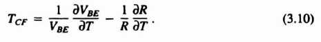
Since the temperature coefficient of the base–emitter junction voltage is negative (−2 m V/°C) while resistors typically have a positive temperature coefficient, the two terms in Eq. (3.9) add, resulting in a net TCF that is quite high. The temperature behavior of the threshold-based bias generator of Fig. 3.3 is similar to the VBE-based circuit.
An alternative supply-independent bias generator is the ΔVBE-based circuit shown in Fig. 3.6a. The operation of this circuit is based on the difference between the base–emitter voltages of two transistors operated at different current densities. In Fig. 3.6a, as in Figs. 3.3 and 3.4, (W/L), = (W/L)2 and (W/L)3 = (W/L)4. Therefore, equal currents flow through the two branches of the circuit and VGS1 = VGS2. Also, the pnp transistor M1, has an emitter area that is m times the emitter area of, M0. The voltage across the resistor R is ΔVBE = VBE0 − VBE1. From Eq. (3.5),
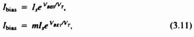
and hence
ΔVBE appears across R and produces a current of value
Obviously, the resulting bias current is independent of the power supply VDD. This circuit also has two operating states: one at the desired operating current given by Eq. (3.13) and the other at zero. To prevent the circuit from operating in the cutoff state, a startup circuit similar to the one shown in Fig. 3.5 is required.
Figure 3.6. (a) ΔVBE-based supply independent bias generator, (b) high-performance ΔVBE-based supply-independent bias generator.
The temperature coefficient of the bias current can be calculated from Eq. (3.13):


Since ∂VT/∂T and ∂R/∂T are both positive, the two terms in the temperature coefficients tend to cancel each other. Thus compared to VBE-or threshold-based bias circuits, the ΔVBE-based bias circuit can produce a much smaller temperature coefficient.
One drawback of the ΔVBE-based bias generator is the strong dependence of Ibias on the mismatches between Q3−Q4 and Q1−Q2 device pairs. The mismatch between Q3−Q4 will result in different currents to flow in the two branches of the circuit. If 1 + ∊ represents the ratio of the two currents, ΔVBE will become
which is equivalent to modifying m, the ratio of the emitter areas, by 1 + ∊. The mismatch between Q1 and Q2 and the current difference due to the mismatch of Q3 and Q4 will make the VGS values of Q1 and Q2 different. This is equivalent to a dc offset voltage Vos = ΔVGS, which modifies Eq. (3.13) to

Assuming that m = 8, ∊ = 0.01, and VT = 26 mV at room temperature, ΔVBE = 26 × ln[8(1 + 0.01)] = 54.3 mV results. For a ΔVGS = 5 mV offset voltage, from Eq. (3.17), Ibias will change by 10%. To reduce this variation special care should be taken in the layout of Q1−Q4. For better geometrical matching, these devices should use a common-centroid layout strategy [2].
The current-matching accuracy of the bias generator of Fig. 3.6a is further degraded due to the mismatch between the drain-to-source voltages of Q3−Q4 and Q1−Q2 transistor pairs. The circuit can be made symmetrical, and the drain-to-source voltage drops equalized, by adding transistors Q5 to Q8 to the two branches of the circuit (Fig. 3.6b). The improved configuration also uses the cascode current mirror principle, described in Section 3.2, to improve the power supply rejection. On the other hand, the minimum power supply voltage is increased compared to the circuit of Fig. 3.6a. due to the extra voltage drops required by the two cascode devices. This becomes a major shortcoming in advanced submicron process technologies, or in low-power/low-voltage applications where the power supply voltage is limited to 3.3 V.
3.2. MOS CURRENT MIRRORS AND CURRENT SOURCES
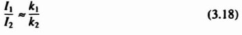
As will be seen in later sections, constant current sources and current mirrors are important components in MOS amplifiers. The MOS current sources are quite similar to the bipolar sources [1,3], where the current mirrors work on the principle that identical devices with equal gate-to-source and drain-to-source voltages carry equal drain currents. An NMOS realization of a current mirror is shown in Fig. 3.7a. In this circuit Q1 is forced to carry a current I1, since its input resistance at its shorted gate–drain terminals is low (much lower than r0), and its gate potential VD1 adjusts accordingly. If Q1 and Q2 are in saturation, their drain currents I1 and I2 are determined to a large extent by their VGS values. Since VGS1 = VGS2 = VG, the condition
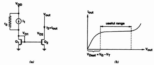
Figure 3.7. (a) n-channel current mirror; (b) output voltage–current relationship and useful output range of the current source.
will therefore hold. More accurately, since drain saturation current is given by

if the transistors have the same λ, k′, and VT, then
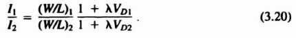
The current I1, is thus “mirrored” in I2.
Using Eq. (3.19) and ignoring the effect of λ, the gate voltage VG is given by
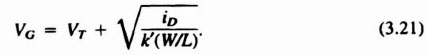
For the transistors to operate in the saturation region, VD ≥ VG − VT must hold. Using Eq. (3.21), therefore, the drain saturation voltage is
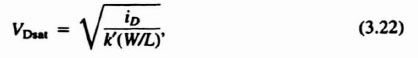
where VDsat is the minimum drain voltage that keeps the transistors in saturation.

Figure 3.8. Small-signal equivalent circuit of the MOS current minor.
For the MOS current source of Fig. 3.7a, the output voltage νout has to be greater than VDsat to keep Q2 in the saturation region. Figure 3.7b shows the output voltage–current relationship of the current source of Fig. 3.7a.
For small-signal analysis, the equivalent circuit of Fig. 2.14 can be used to model Q1 and Q2. The resulting circuit is shown in Fig. 3.8. Here ro is the incremental resistance of the current source I1 and νin is the test voltage connected to the drain of Q2 for measuring the output impedance of the circuit. The small-signal output impedance is simply

where Eq. (3.19) was used.
Clearly, the current source of Fig. 3.7a has an output impedance that is not better (i.e., higher) than the output impedance of a simple MOS transistor, also inaccurate current matching due to the variation of the drain voltage of Q2 with the output voltage, and finally a reasonably wide output voltage range, which is limited at the lower end by VDsat.
The output impedance rout, can be increased, and thus the circuit made to perform more like an ideal current source, by adding one more device and modifying the connections slightly. The resulting circuit (Fig. 3.9) is the MOS equivalent of Wilson's current source [1,3]. In this circuit, if I2 increases, Q2 causes ν1 to become larger. This results in a drop of ν3 which then counteracts the increase of I2. Thus a negative feedback loop exists, which tries to hold I2 constant. The small-signal equivalent circuit is shown in Fig. 3.10; a simplified circuit is shown in Fig. 3.11. The latter was obtained by combining ro and rd1, into ![]() , by replacing the self-controlled current source gm2ν2 by a resistor 1/gm2, and by neglecting rd2 which is now parallel with the (usually much smaller) resistor 1/gm2. Solving for iin in Fig. 3.11 gives
, by replacing the self-controlled current source gm2ν2 by a resistor 1/gm2, and by neglecting rd2 which is now parallel with the (usually much smaller) resistor 1/gm2. Solving for iin in Fig. 3.11 gives
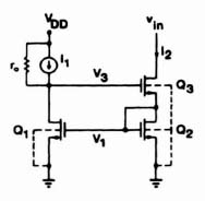
Figure 3.9. MOS version of Wilson's current source.

Figure 3.10. Small-signal equivalent circuit of Wilson's current source.

Typical values for gm are around 1 mA/V, while rd is on the order of hundreds of kiloohms. Hence gm3rdB ![]() 1 and for reasonably large ro, gm1r1
1 and for reasonably large ro, gm1r1 ![]() 1. Then, from Eq. (3.24),
1. Then, from Eq. (3.24),

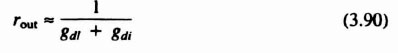
Here, on the right-hand side the value of the first factor is around 100, while that of the second is around 1. Hence the output impedance rout is two orders of magnitude larger than rd3. The output impedance of the current source drops as soon as transistor Q3 enters the linear (triode) region. The minimum level of the output voltage swing of the Wilson's current source is thus limited to Vmin = VGS2 + VDsat3. In summary, the characteristics of Wilson's current source are the following: high output impedance, restricted output voltage swing, and poor current-matching accuracy, due to the mismatch between the drain-to-source voltages of transistors Q1, and Q2.

Figure 3.11. Simplified small-signal equivalent circuit of Wilson's current source.

Figure 3.12. Improved MOS Wilson's current source.
The circuit can be made symmetrical, and the drain–source voltage drops of Q1, and Q2 equalized, by adding another transistor, Q4 (Fig. 3.12). It can easily be shown that the output impedance of the resulting improved MOS Wilson's current source is again given by Eq. (3.25). The detailed analysis of the circuit is left to the reader (Problem 3.6a).
A slightly better version of the circuit of Fig. 3.12 (often called cascode current source) is shown in Fig. 3.13a. Its small-signal equivalent circuit is shown in Fig. 3.13b and in a simplified form in Fig. 3.13c. This circuit also uses feedback to maintain I2 constant, and it also equalizes the drain potentials of Q1 and Q2, thus improving the current-matching properties of the current mirror. It can easily be shown (Problem 3.6b) that now
Hence there is again a 100-fold increase over the single-MOSFET output resistance. In addition, now the internal impedance ro of the current source I1 is in parallel with 1/gm1 + 1/gm4, a low input impedance, rather than with rd1. Hence its loading effect is much reduced.
The cascode current source is similar to the improved Wilson's current source: It is characterized by high output impedance and accurate current mirroring capability. However, a common disadvantage of both circuits is that the minimum level of the output voltage swing is higher than that of the simple current mirror of Fig. 3.7. This reduces the available voltage swing of the stage(s) driven by the mirror. For the circuit of Fig. 3.13, the minimum voltage swing before Q3 makes the transition from the saturation region to the linear region is
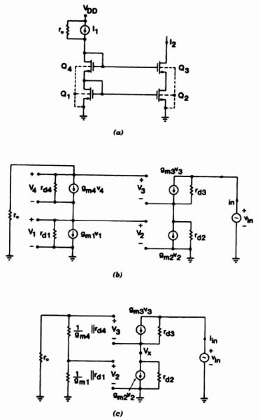
Figure 3.13. (a) Cascode current source; (b) equivalent small-signal circuit of the cascode current source; (c) simplified small-signal circuit of the cascode current source.
The output voltage–current plot for the cascode current source is shown in Fig. 3.14. The plot shows three operating regions. In the region where both Q2 and Q3 are in saturation (VD ≥ VT + 2VDsat) the output impedance has the highest value. In the region where Q2 is in saturation and Q3 is the linear region (2VDsat ≤ VD < VT + 2VDsat), the output impedance is substantially lower. When VD < 2VDsat, both transistors are in their linear regions, and the output impedance is very low.
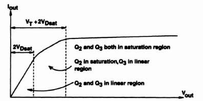
Figure 3.14. Output voltage–current relationship for cascade current source.
As mentioned earlier, a major drawback of the cascode current source is its limited output voltage swing. As Eq. (3.27) shows, the minimum voltage at the output of the current source that keeps both Q2 and Q3 in saturation is now VT + 2VDsat. This loss of voltage swing is especially important when the current source is used as the load of a gain stage. To reduce the loss and increase the output swing, we can bias the drain of the lower transistor Q2 at the edge of the saturation region. The resulting high-swing cascode current source is shown in Fig. 3.15 [4].
In this circuit a source follower (Q5 and Q6) has been inserted between the gates of Q3 and Q4 in Fig. 3.13a, and the W/L ratio of Q3 has been reduced by a factor of 4. Using the simplified MOS I–V equation ID = k′ W/L(VCS − VT)2 for the saturation region, and the W/L ratios given in Fig. 3.15, we have

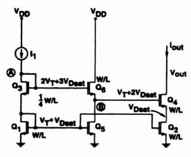
Figure 3.15. High-swing cascode current source.

Figure 3.16. High-swing improved current source.
where ![]() . From Fig. 3.15, the node voltages VA, VB and VDS2 can be found:
. From Fig. 3.15, the node voltages VA, VB and VDS2 can be found:
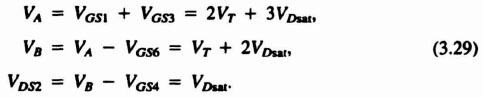
Q2 is therefore biased at the edge of saturation. The lowest level of the output voltage swing is now limited to 2VDsat, which is a major improvement compared to that of the circuit of Fig. 3.13a. The high-swing cascode current source exhibits a high output impedance, similar to that of the cascode current source, and an improved output voltage swing. The current matching, however, suffers due to the mismatch in the drain-to-source voltages of the mirror transistors Q1, and Q2. For Q1, VDS1 = VT + VDsat, while for Q2, VDS2 = VDsat.
An improved high-swing cascode current source, along with its biasing circuit, is shown in Fig. 3.16. Here n is a positive-integer number [5, p. 560]. Once again, using the simplified MOS I–V equation results in

where (VDsat)W/L. is the minimum drain-to-source voltage required to keep devices Q1 and Q3 with a current I and aspect ratio W/L in saturation. For devices Q3 and Q5 we have

Using Eq. (3.31) yields

Clearly, since VDS1 = VDS2 = (VDsat)W/L, both Q1, and Q2 are biased at the edge of their saturation regions. Also, assuming that VDS3 = VT ≥ VDsat3 = n(VDsat)W/L, Q3 will be biased in the saturation region. As a result, the circuit will have a high output impedance. Notice that the output node νout has high-swing capability. Actually, as long as νout is greater than (n + 1)(VDsat)W/L, the output will maintain its large output impedance. For the improved current mirror the devices Q1 and Q2 have equal VGS as well as equal VDS values and therefore good current-matching capability.
The formulas and numerical estimates given for the current sources are somewhat optimistic since they neglect the body effect of the floating devices (transistors Q3 and Q4 in Figs. 3.13 to 3.16). Also, real MOS transistors do not display an abrupt transition from the saturation to Unear region. Therefore, it is necessary to bias the drain voltages of the mirror devices Q1 and Q2 slightly above the ideal saturation voltage produced by ![]() to achieve the high output impedance derived earlier.
to achieve the high output impedance derived earlier.
3.3. MOS GAIN STAGES [6–8]
A simple NMOS gain stage with resistive load is shown in Fig. 3.17. Q1 is biased so that it operates in its saturation region. The low-frequency small-signal equivalent circuit is shown in Fig. 3.18. The voltage gain of the stage is clearly

In integrated-circuit realization, the resistor RL is undesirable since it occupies a large area and introduces a large voltage drop and hence is usually replaced by a second MOSFET. If an NMOS enhancement-mode device is used as a load, the circuit of Fig. 3.19 results. The drain and gate of Q2 are shorted to ensure that νds > νgs − VT, and hence the device is in saturation. The small-signal equivalent circuit of the load device Q2 alone is shown in Fig. 3.20. Here the voltage-controlled current source gmνds is across the voltage νds; hence it behaves simply as a resistor of value 1/gm. Similarly, since νsb = νout, the source gmbνsb corresponds to a resistor 1/|gmb| [recall that by Eq. (2.19), gmb < 0!]. In conclusion, Q2 behaves like a resistor of value 1/gm2 + |gmb2 + gd2). Replacing RL in Fig. 3.17 by this resistor and neglecting gd1, and gd2 in comparison with gm2 + |gmb2| gives

Figure 3.17. Resistive-load MOS gain stage.
Figure 3.18. Small-signal low-frequency equivalent circuit of the resistive-load gain stage.
If the body effect is small, so that |gmb2| ![]() gm2, then using Eq. (2.18),
gm2, then using Eq. (2.18),
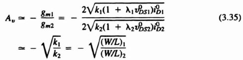
results. Here the channel-modulation terms ![]() were also neglected, and the relations iD1 = iD2 and
were also neglected, and the relations iD1 = iD2 and ![]() utilized.
utilized.
The sad message conveyed by Eq. (3.35) is that a large gain can be obtained only if the aspect ratio W/L of Q1 is many times that of Q2. If, for example, a gain of 10 is required, (W/L)1 = 100(W/L)2 must hold. This is possible only if a large silicon area is used. In addition, the body effect also reduces the gain significantly.
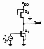
Figure 3.19. Enhancement-load NMOS gain stage.
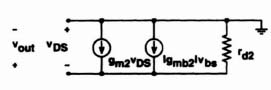
Figure 3.20. Small-signal equivalent circuit of the enhancement-load device Q2.
Including body effect (but still neglecting channel-length modulation), using Eqs. (2.12), (2.19), and (3.34),

results. For |![]() p| = 0.3 V,
p| = 0.3 V, ![]() , = 5 V, and γ = 1, the denominator is 1.21; hence the gain is reduced from 10 to 8.26.
, = 5 V, and γ = 1, the denominator is 1.21; hence the gain is reduced from 10 to 8.26.
In conclusion, the NMOS enhancement-load gain stage provides a low gain. This stage is nonetheless often useful in wideband amplifiers, where a low but predictable gain can be tolerated and the gain stage exhibits a wide bandwidth due to the low resistance of the load. For high-gain applications, however, the stage needs a large silicon area and since the load device has a high resistance (small W/L ratio), it has a large dc voltage drop across it which reduces the signal-handling capability and hence the dynamic range of the stage.
To improve the performance and increase the gain of the MOS amplifiers, a current–source load can be used. Any of the current sources described in the earlier sections can serve as a load. A common-source MOS gain stage that uses an NMOS input device and the p-channel version of the simple current source of Fig. 3.7a is shown in Fig. 3.21. The operation of this circuit is similar to the resistive-load gain stage of Fig. 3.17, but the resistive load is replaced by the small-signal output impedance rd1 of the PMOS current source. Using Eq. (3.33), the gain of the CMOS amplifies stage is
For gm1 = 0.2 mA/V and rd1 = rd2 = 1 MΩ, the small-signal low-frequency gain is Aν = −100. Obviously, the gain is proportional to the transconductance of the input device and the small-signal output resistance of the stage r0 = rd1 || rd2. Since rd ![]() 1/gm for a given size of the load device, large values of gain can be achieved in a moderately small silicon area. Using a cascode current source with significantly higher output impedance will not increase the gain of the amplifier directly, because the output resistance of the stage is limited by the output impedance of the input device.
1/gm for a given size of the load device, large values of gain can be achieved in a moderately small silicon area. Using a cascode current source with significantly higher output impedance will not increase the gain of the amplifier directly, because the output resistance of the stage is limited by the output impedance of the input device.

Figure 3.21. Common-source gain stage with NMOS input and p-channel current source as active load.

Figure 3.22. Enhancement-load gain stage with capacitive load.
For the gain stage of Fig. 3.21 to operate properly, both input and load devices should operate in their saturation regions. The output signal swing is thus limited to VDD − |VDsat2 and VDsat1 on the positive and negative side, respectively. The output signal must therefore remain in the range
and the total output swing is
For high-frequency applications, all gain stages discussed so far have a common shortcoming. Consider the circuit of Fig. 3.22, which includes the source resistance RS and the capacitive load CL of the gain stage. Including the parasitic capacitances in the small-signal equivalent circuit, the diagram shown in Fig. 3.23a is obtained. Combining parallel-connected elements, the circuit of Fig. 3.23b results, where

The node equations for nodes A and B are
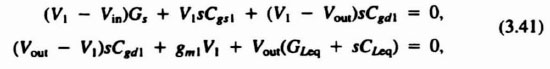
where all voltages are Laplace-transformed functions.
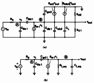
Figure 3.23. (a) Equivalent circuit of the MOS gain stage; (b) simplified equivalent circuit of the MOS gain stage.
Solving Eq. (3.41) gives

To obtain the frequency response, s must be replaced by jω. For moderate frequencies, ![]() hold. Then a good approximation is
hold. Then a good approximation is
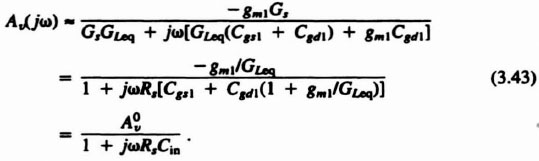

Figure 3.24. Approximate equivalent circuit of the MOS gain stage.
Here ![]() is the dc value of Aν(jω), and
is the dc value of Aν(jω), and

Aν(jω) in Eq. (3.43) can be recognized as the transfer function of the circuit shown in Fig. 3.24. Thus the capacitor Cgd1 which is connected between the input and output terminals of the gain stage (Fig. 3.23a) behaves like a capacitance ![]() times its real size, loading the input terminal. This is the well-known Miller effect [2]. For
times its real size, loading the input terminal. This is the well-known Miller effect [2]. For ![]() , the high-frequency gain will be seriously affected and the bandwidth considerably reduced by this phenomenon.
, the high-frequency gain will be seriously affected and the bandwidth considerably reduced by this phenomenon.
To prevent the Miller effect, the cascode gain stage of Fig. 3.25 can be used. Here Q2 is used to isolate the input and output nodes. It provides a low input resistance 1/gm2 at its source and a high one at its drain to drive Q3. Ignoring the body effect, the low-firequency small-signal equivalent circuit is in the form shown in Fig. 3.26. Neglecting the small gd admittances, clearly
Hence, for low frequencies.

Figure 3.25. Cascode gain stage with enhancement load.

Figure 3.26. Low-frequency small-signal circuit of cascode gain stage.
The gate-to-drain gain of Q1 is −gm1gm2, and therefore the Cgd1 of the driver transistor Q1 is now multiplied by (1 + gm1/gm2). Choosing gm1 = gm2, this factor is only 2. The overall voltage gain −gm1/gm3, however, can still be large, without introducing significant Miller effect, since there is no appreciable capacitance between the input and output terminals.
As before, the gain of the cascode gain stage can be increased by using a current mirror as an active load device. A cascode amplifier with a p-channel current source as active load is shown in Fig. 3.27. It can readily be shown that the low-frequency voltage gain of this circuit is given by
where, as derived earlier [cf. Eqs. (3.23) and (3.26)],
The value of rout2 is much larger than rout1 because of the local feedback. The effective output impedance is therefore given by
and the gain of the stage is
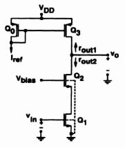
Figure 3.27. Cascode stage with p-channel current source as active load.

Figure 3.28. Cascode stage with p-channel cascode current source as active load.
To exploit fully the availability of the high output impedance rout2 for high gain, a cascode current source must be used for the active load. A cascode gain stage with a p-channel cascode current source as active load is shown in Fig. 3.28. The value of the load resistance is given by
Assuming that rout1 = rout2, we have
and the gain is given by

Since ro is much larger than ro3, the gain Aν can be much larger than the gain of a stage with a simple current source.
To improve the output signal swing, a biasing strategy similar to the high-swing cascode current source should be used, so that both Q1 and Q3 are biased only slightly above the saturation region. The maximum output signal swing is given by
The use of a cascode current source as an active load in the gain stage of Fig. 3.28 provides a high voltage gain that is sufficient for the majority of the applications.
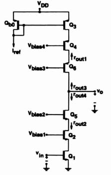
Figure 3.29. Gain stage with double-cascode input and double-cascode load.
However, in cases where an extremely high gain is required, the cascoding concept for the current sources can be extended by stacking more devices in the ease ode configuration, which increases the output impedance and hence the voltage gain. A double cascode gain stage with double cascode active load is shown in Fig. 3.29. Compared to Fig. 3.28, two additional devices in a common-gate configuration have been added to the cascode input and cascode load. Using the results expressed in Eq. (3.51), the output impedance rout3 can be calculated as
Combining Eqs. (3.51) and (3.55), we have
Similarly, rout4 can be calculated as
Once again if we assume that rout3 ≈ rout4, the voltage gain becomes
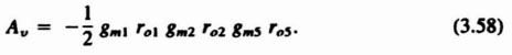
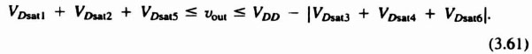
The resulting gain is quite high and is proportional to gmro raised to the third power. The high gain is achieved at the cost of reduced output swing. To maximize the output voltage swing, once again Q1, Q2, Q3, and Q4 should be biased slightly above the saturation region. The bias voltages are therefore given by
Similar equations can be derived for Vbias3 and Vbias4. Using these results, the maximum output signal swing is limited to the following range:
Another technique to improve the output impedance of the cascode current source of Fig. 3.28 is to place Q2 in a feedback loop that senses the drain voltage of Q1 and adjust the gate of Q2 to minimize the variation of the drain current. A simplified form of this circuit is shown in Fig. 3.30, where the gain stage reduces the feedback from the drain of Q2 to the drain of Q1 [9]. Thus the output impedance of the circuit is increased by the gain of the additional gain stage, A:
Similarly, the output impedance rout1 can be calculated as
Assuming that rout1 ≈ rout2, the voltage gain of the stage is given by
which has been increased by several orders of magnitude.
A simple implementation of the circuit of Fig. 3.30 is shown in Fig. 3.31, where the feedback amplifier is realized as a common-source amplifier consisting of transistor Q5 and the corresponding current source IB1 [10]. The operation principle of the circuit of Fig. 3.31 is described briefly as follows. The transistor Q1 converts the input voltage νi into a drain current that flows through Q1 and Q2 to the output terminal. For high output impedance the drain voltage of Q1 must be kept stable. This is accomplished by the feedback loop consisting of the amplifier (Q5 and IB1) and Q2 as a source follower. In this way the drain–source voltage of Q1 is regulated to a fixed value. The disadvantage of the circuit of Fig. 3.31 is that it limits the output swing, because the drain voltage of Q1 is VGS5, where as it can be as low as VDsat1 = VGS1 − VT. Additionally, the gate-to-drain capacitance of Q5 multiplied by the gain of the feedback amplifier (Q5 and IB1) forms a low-frequency pole with 1/gm2. which degrades the high-frequency performance of the main amplifier stage.

Figure 3.30. Cascode gain stage with enhanced output impedance.
Folded-cascode op amps, presented in Chapter 4, can be used for the feedback amplifier. One example of this type of implementation is shown in Fig. 3.32, where PMOS and NMOS input folded-cascode op-amps have been used to enhance the output impedance of the NMOS and PMOS cascode stages [9]. To maximize the output voltage swing, Vbias1 = VGS1 − VTν and Vbias3 = VDD + (VGS4 − VTp) should hold. Folded-cascode op-amps are described in detail in Chapter 4.

Figure 3.31. Simple implementation of Fig. 3.30.

Figure 3.32. Complete circuit diagram of a gain-enhanced cascode amplifier employing folded-cascode op-amps as feedback amplifiers.
3.4. MOS SOURCE FOLLOWERS [5–8]
MOS source followers are similar to bipolar emitter followers. They can be used as buffers or as dc level shifters. The basic source follower, with an NMOS input device and an NMOS current source as an active load, is shown in Fig. 3.33 and its small-signal low-frequency equivalent circuit in Fig. 3.34. The node current equation for the output node is
Substituting νgs1 = νin − νout and solving yields
Hence ![]() .
.

Figure 3.33. Basic structure of MOS source follower.
The output impedance of the source follower can be calculated by applying a test source νx at its output (Fig. 3.35). The current law gives
Here νgs1 = −νx, and hence Eq. (3.67) gives
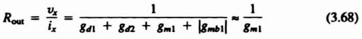
since usually gm1 ![]() gd1, gd2, and |gmb1|. Thus Rout has a relatively low value, on the order of 1 kΩ.
gd1, gd2, and |gmb1|. Thus Rout has a relatively low value, on the order of 1 kΩ.
The dc bias current of the stage is determined by the current source Q2, which drives Q1 at its low-impedance source terminal. Thus the dc drop VGS1 between the input and output terminals is determined by Vbias. and the dimensions of Q1 and Q2; these parameters can be used to control the level shift provided by the stage.
The gate of the load device Q2 may be connected to its drain to eliminate the gate bias voltage (Fig. 3.36). Analysis shows that for gm2 ![]() gd1, |gmb1|, the voltage gain is then (1 + gm2/gm1)−1. This can be close to 1 only if gm1,
gd1, |gmb1|, the voltage gain is then (1 + gm2/gm1)−1. This can be close to 1 only if gm1, ![]() gm2, which as discussed in connection with Fig. 3.35, requires a large area for the stage. Hence this stage is rarely used.
gm2, which as discussed in connection with Fig. 3.35, requires a large area for the stage. Hence this stage is rarely used.
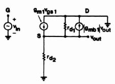
Figure 3.34. Small-signal low-frequency equivalent circuit of the source follower.
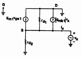
Figure 3.35. Equivalent circuit to calculate the output impedance of the source follower.
The large-signal operation of the circuit can be analyzed simply if the load device is regarded as a current source. Figure 3.37 shows the redrawn circuit; ro is the average large-signal output resistance of the current source and RL is the load resistor. From Eq. (2.9), ignoring the body effect.
If (go + GL/k1 ![]() 2|νin − VT1|, then
2|νin − VT1|, then
so that the circuit operates as a linear buffer with a constant offset. To achieve this, (W/L)1 must be sufficiently large.
A major disadvantage of this stage is the following. If νout < 0, the load supplies current to the output stage. However, the latter can sink (absorb) an output current only if it is less than Io. This represents a serious limitation. Also, for νout ![]() 0, Q1 must supply the output current plus I0. In addition, there is a voltage drop greater then VT1 between the input and output terminals. Thus if νin comes from a gain stage such as that shown in Fig. 3.19, where the output voltage must be less than VDD − VT2, the maximum positive output voltage swing is VDD − 2VT. The negative swing is limited by the requirement that the device(s) in the current source must remain in saturation for the smallest output voltage.
0, Q1 must supply the output current plus I0. In addition, there is a voltage drop greater then VT1 between the input and output terminals. Thus if νin comes from a gain stage such as that shown in Fig. 3.19, where the output voltage must be less than VDD − VT2, the maximum positive output voltage swing is VDD − 2VT. The negative swing is limited by the requirement that the device(s) in the current source must remain in saturation for the smallest output voltage.
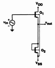
Figure 3.36. Enhancement-load source follower.

Figure 3.37. Source follower with a current source as load.
3.5. MOS DIFFERENTIAL AMPLIFIERS
The input stage of an operational amplifier must provide a high input impedance, large common-mode rejection ratio (CMRR) and power supply rejection ratio (PSRR), low dc offset voltage and noise, and most (or all) of the op-amp's voltage gain (accurate definitions of these terms are given in Chapter 4). The output signal of the input stage is much larger than the input one and so is no longer as sensitive to noise and offset voltage generated in the following stages. (Note that a large common-mode rejection is desirable even if the noninverting terminal is grounded in normal operation, to suppress noise in the ground line.)
The requirements above can often be met by using the source-coupled stage shown in Fig. 3.38. Since this circuit operates in a differential mode, it can provide high differential gain along with a low common-mode gain and hence ensure a large CMRR. The differential configuration also helps in achieving a large PSRR, since variations of VDD are, to a large extent, canceled in the differential output voltage νo1 − νo2.
An approximate analysis of the amplifier can readily be performed. We assume that the current source I is ideal, that is, that its internal conductance g is zero. We also assume ideal symmetry between Q1, and Q2 and Q3 and Q4, and all devices operate in saturation. Then the incremental drain currents satisfy id1 ≈ gmi (νin1 − ν), id2 ≈ gmi(νin2 − ν), and id1 + id2 ≈ 0. This gives ν ≈ (νin1 + νin2)/2 for the source voltages of Q1 and Q2, and id1 ≈ −id2 ≈ gmi(νin1 – νin2)/2 for their drain currents. Hence the output voltages are νo1 ≈ −νo2 = −id1/g1 = gmi(νin1 − νin2)/2g1, where g1, is the load conductance. Defining the differential gain by ![]() . we obtain the simple result Adm ≈ −gmi/g1. Thus the differential gain is the same as for a simple inverter, however, the stage also provides a rejection of common-mode signals and of noise in the power supplies VDD and VSS, all of which are canceled (or, for actual circuits, reduced) by the differential operation of the stage. A more detailed analysis follows.
. we obtain the simple result Adm ≈ −gmi/g1. Thus the differential gain is the same as for a simple inverter, however, the stage also provides a rejection of common-mode signals and of noise in the power supplies VDD and VSS, all of which are canceled (or, for actual circuits, reduced) by the differential operation of the stage. A more detailed analysis follows.

Figure 3.38. Source-coupled differential stage with diode-connected NMOS load devices.
The low-frequency small-signal equivalent circuit of the source-coupled stage is shown in Fig. 3.39. In the circuit, the body-effect transconductances of the input devices Q1 and Q2 are ignored to simplify the discussions. It will also be assumed that the circuit is perfectly symmetrical, so that the parameters of Q1, and Q2 are identical, as are those of Q3 and Q4. The load conductance g1 of Q3 and Q4 can be found as was done in connection with Fig. 3.20: the result is

Figure 3.39. Small-signal equivalent circuit of the source-coupled pair.
Applying the current law at nodes A and B,

result. (Here the subscripts i and l refer to the input and load devices, respectively.) The current law at node C gives

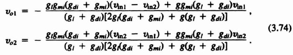
Equations (3.72) and (3.73) represent three equations in the three unknowns νo1, νo2, and ν. Solving them for νo1 and νo2, we get
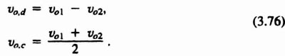
The differential and common-mode input voltages are

The differential and common-mode output voltages can be defined similarly:
Then the differential-mode gain can be obtained from Eq. (3.74):

For g = 0 and gdi ![]() gl, Adm ≈ −gmi/g1 as predicted earlier. Similarly, the common-mode gain can be found:
gl, Adm ≈ −gmi/g1 as predicted earlier. Similarly, the common-mode gain can be found:

Hence the common-mode rejection ratio is

Normally, g, gdi ![]() gl, gmi and approximations
gl, gmi and approximations
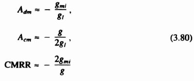
can be used. Clearly, to obtain a large CMRR, g must be small; that is, the current source should have a large output impedance. The circuits described earlier and shown in Figs. 3.7 to 3.16 are suitable to achieve this. All, however, require a dc voltage drop for operation which limits the achievable output voltage swing.
As Eq. (3.80) indicates, with the described approximation (including the assumed absence of the body effect), the differential gain can be obtained from
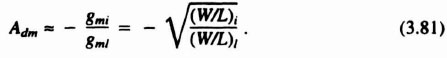
Obviously, a large gain can be achieved only if the aspect ratio (W/L)i, of the input devices is many times that of the load devices (W/L)i. A somewhat improved version of the differential stage of Fig. 3.38 can be obtained by using PMOS devices Q3 and Q4 as loads (Fig. 3.40). For this circuit Eqs. (3.77) to (3.80) remain valid; however, the differential gain Adm is larger and is given by

where μn and νp are the mobilities of the NMOS and PMOS devices, respectively.
The gain of the differential stage of Fig. 3.40 can be increased by using a controlled amount of positive feedback to increase the transconductance of the input device [11]. The resulting circuit is shown in Fig. 3.41 and the differential gain can be derived as

Figure 3.40. Source-coupled CMOS differential stage with diode-connected PMOS load devices.

where α = (W/L)5/(W/L)3. As an example, if ![]() , the differential gain will be increased by a factor of 4.
, the differential gain will be increased by a factor of 4.
All the differential stages described thus far have low gain and a differential output voltage. For high gain the circuit of Fig. 3.42a can be used. This circuit has differential input but single-ended output. Hence it performs as a combination of a differential gain stage and a differential-to-single-ended converter. In Fig. 3.42a transistors Q1–Q2 and Q3–Q4 form matched transistor pairs. They have equal W/L ratios. All current levels are determined by the current source Io, half of which flows through Q1–Q3 and the other half flows through Q2–Q4. All transistors have their substrates connected to their sources to eliminate body effect and improve matching.
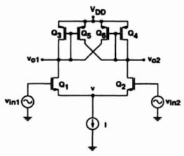
Figure 3.41. Source-coupled CMOS differential stage with positive feedback to increase gain.

Figure 3.42. (a) CMOS differential stage with active load; (b) small-signal equivalent circuit for CMOS differential stage.
An approximate analysis of the circuit can readily be performed as follows. Assuming that the current source I0 is ideal, the incremental drain currents of Q1 and Q2 must satisfy id1 + id2 = 0. Also, if both Q1 and Q2 are in saturation, then id1 ≈ gmi(νin1 − ν1) and id2 ≈ gmi(νin2 − ν1). Combining these equations, ν1 ≈ (νin1 + νin2)/2 results. Hence id1 = −id2 ≈ gmi(νin2 − ν1)/2. The current id1 is easily imposed on Q3 by Q1, since the impedance at the common terminal of the gate and drain of Q3 is only 1/gm3.
Transistors Q3 and Q4 form a current mirror similar to that shown in Fig. 3.7a, and hence the current through Q4 satisfies id4 = id3 = id1. Thus both Q2 and Q4 send a current id1 = gmi(νin1 − νin2)/2 into the output terminal. Since the output is loaded by the drain resistances of Q2 and Q4, the differential gain is thus ![]() . A more exact analysis follows next.
. A more exact analysis follows next.
The small-signal equivalent circuit of the stage is shown in Fig. 3.42b. It was drawn under the assumption that both input devices Q1 and Q2 have the same conductances gmi and gdi, and that both load devices have the parameters gml and gdl; also, that separate “wells” are provided for the PMOS devices. Then νBS = 0 for all devices, and hence no body effect occurs. The output conductance of the current source is denoted by go.
Writing and solving the current law equations for nodes A, B, and C (Problem 3.11), we obtain
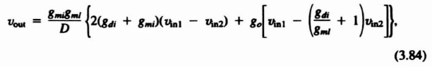
where
![]()
We define, as before, the differential and common-mode input signals by Eq. (3.75). Then the differential gain Adm and the common-mode gain Acm can be defined by
From Eqs. (3.84) and (3.85),
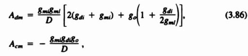

For gmi, gml, ![]() go, gdi, and gdl the approximations
go, gdi, and gdl the approximations

can be used. Note that Adm is the same as that obtainable from a CMOS differential-input/differential-output stage (Problem 3.12). Thus the single-ended output signal does not result in lower gain for the stage. By contrast, the CMRR is higher by a factor of gmi/gdi, which (for usual values) is much greater than 1.

Figure 3.43. Equivalent circuit of the output impedance of the CMOS differential stage.
To calculate the small-signal output impedance of the CMOS stage, a test source io can be applied at the output of the small-signal equivalent circuit and the input voltages νin1 and νin2 set to zero (Fig. 3.43). Analysis shows (Problem 3.13) that

where D is defined in Eq. (3.84).
For gmi, gml ![]() go, gdi, gdl, the approximation
go, gdi, gdl, the approximation
can be used.
3.6 FREQUENCY RESPONSE OF MOS AMPLIFIER STAGES
In previous sections the linearized (small-signal) performance of MOS amplifier stages was analyzed at low frequencies. Thus the parasitic capacitances illustrated in the equivalent circuit of Fig. 2.16 were ignored. For high-frequency signals, however, the admittances of these branches are no longer negligible, and hence neither are the currents which they conduct. Then the gains and the input impedances of the various circuits all become functions of the signal frequency ω. These effects are analyzed next.
Consider again the all-NMOS single-ended amplifier (Fig. 3.22), discussed in Section 3.3. Using the equivalent circuit of Fig. 2.16, the high-frequency small-signal equivalent circuit of Fig. 3.23a resulted. In the circuit, Rs is the output impedance of the signal source and CL is the load capacitance. This circuit was then simplified to that of Fig. 3.23b, which (in the Laplace transform domain) was shown to have the frequency response given in Eq. (3.42). With the approximations gm1 ![]() ωCgd1, GLeq
ωCgd1, GLeq ![]() ω(Cgd1 + CLeq, the frequency response of Eq. (3.49) resulted. It corresponded to the simplified equivalent circuit of Fig. 3.24, which was then used to introduce the Miller effect.
ω(Cgd1 + CLeq, the frequency response of Eq. (3.49) resulted. It corresponded to the simplified equivalent circuit of Fig. 3.24, which was then used to introduce the Miller effect.

Figure 3.44. Simplified equivalent circuit of the MOS gain stage using Miller's theorem.
The accuracy of the simplified circuit can be improved by restoring the two capacitances CLeq and Cgd1 which load the output node in the exact circuit of Fig. 3.23b. Also, in the numerator of Eq. (3.42), the term sCgd1 was neglected in comparison with gm1. At higher frequencies, this is no longer justified. To restore the sCgd1 term, the gain of the controlled source gm1 can be changed to gm1 − sCgd1 in the equivalent circuit. The resulting circuit is shown in Fig. 3.44. The corresponding transfer function is
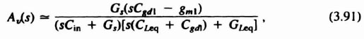
where Cin is given by Eq. (3.44). This function has a right-half-plane (positive) real zero at
and two left-half-plane (negative) poles at
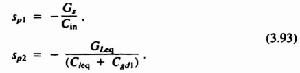
Normally, Cgd1 is small. Hence sz ![]() |sp1|, and if CLeq is also small, then |sp2|
|sp1|, and if CLeq is also small, then |sp2| ![]() |sp1|. Then sp1 is closest to the jω axis and is therefore the dominant pole of the circuit.
|sp1|. Then sp1 is closest to the jω axis and is therefore the dominant pole of the circuit.
The frequency response Aν(jω) can be obtained simply by replacing s by jω in (3.91). It can be arranged in the form

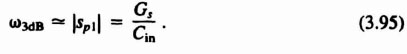
If |sp1| ![]() |sp2| and sz, the 3-dB frequency (i.e., the frequency where |Aν(jω)| is 1/
|sp2| and sz, the 3-dB frequency (i.e., the frequency where |Aν(jω)| is 1/![]() times its dc value) is
times its dc value) is
For high gain, an active (current-source) load can be used. A CMOS gain stage with a p-channel current source as active load and capacitive loading is shown in Fig. 3.45a; the corresponding high-frequency linear equivalent circuit in Fig. 3.45b. Defining
the simplified circuit of Fig. 3.45c results.
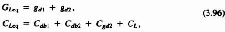
Using the approximation yielding Fig. 3.44 for the NMOS gain stage, the circuit of Fig. 3.45d can be obtained. Obviously, the circuit in Fig. 3.45d is identical to that in Fig. 3.44d, and hence the transfer function of Eq. (3.91) is also valid for the circuit of Fig. 3.45d. The poles and the zero are also given by Eqs. (3.92) and (3.93). The dominant pole is normally sp1 = −Gs/Cin. Notice, however, that GLeq in Fig. 3.45 is gd1 + gd2, while in Fig. 3.44 it is gd1 + gd2 + gm2 + gmb2. Since the former is much smaller, sp2 for the circuit of Fig. 3.45 is at a much lower frequency than that of Fig. 3.44.
Figure 3.46a shows a CMOS cascode gain stage with an active load. CL represents the capacitive load of the stage. Figure 3.46b and c show the detailed and simplified high-frequency linearized equivalent circuits, respectively. Using Miller's theorem, the circuit of Fig. 3.46d results, where
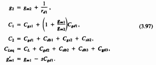

Figure 3.45. (a) CMOS gain stage with active load and capacitive loading; (b) equivalent circuit of the CMOS gain stage; (c) simplified equivalent circuit of CMOS gain stage; (d) simplified equivalent circuit of CMOS gain stage using Miller's theorem.

Figure 3.46. (a) Active-load cascode stage with capacitive loading; (b) high-frequency equivalent circuit of the cascode stage; (c) simplified high-frequency equivalent circuit of the cascode stage; (d) simplified equivalent circuit of the cascode stage obtained using Miller's theorem.
The circuit of Fig. 3.46d can easily be analyzed (thanks to the Miller approximation, which neatly partitioned it into buffered sections). The result is
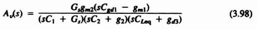
from which the zero and the poles can be recognized direcdy:
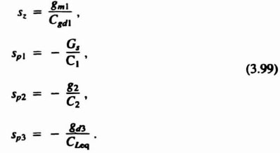
For practical values, usually |sp1 ![]() sz, |sp2|, |sp3. Then sp1 is the dominant pole, and the 3-dB frequency is given by
sz, |sp2|, |sp3. Then sp1 is the dominant pole, and the 3-dB frequency is given by
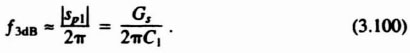
Typically, gm1 = gm2; then C1 = Cgs1 + 2Cgd1 and f3dB ≈ Gs/[2π(Cgs1, + 2Cgd1)]. By contrast, for the simple inverter stage of Fig. 3.45a the corresponding value is Gs/{2π[Cgs1 + (1 + gm1/GLeq)Cgd1]}, as Eqs. (3.91) and (3.52) show. Since gm1/GLeq is the magnitude of the dc gain of the stage, it is usually large. Hence the dominant pole (and thus the 3-dB frequency) is much smaller for the simple gain stage than for the cascode circuit. This confirms the effectiveness of the latter for high-frequency amplification.
The analysis of the NMOS source follower is straightforward. Figure 3.47a shows the actual circuit; Fig. 3.47b and c show the high-frequency small-signal equivalent circuits. The transfer function can be readily derived (Problem 3.15); the result is

where
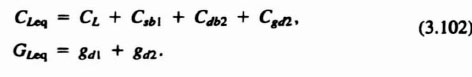
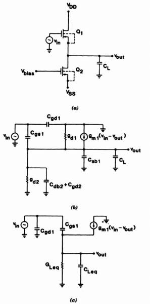
Figure 3.47. (a) NMOS source follower with capacitive loading; (b) equivalent circuit of the NMOS source follower; (c) simplified equivalent circuit of the NMOS source follower.
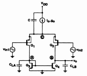
Figure 3.48. CMOS differential stage with capacitive loading. Circuit for Problem 3.2.
The zero and the pole are hence
and
Choosing GLeq/gm1 ![]() CLeq/Cgs1, sz
CLeq/Cgs1, sz ![]() sp can be achieved. Then Aν(s)
sp can be achieved. Then Aν(s) ![]() Cgs1/(Cgs1 + CLeq), and hence the gain is constant up to very high frequencies, where higherorder effects cause it to drop. In the actual implementation, in order to meet the condition on CLeq/Cgs1, it may be necessary to connect a capacitor C in parallel with Cgs1, that is, between the input and output terminals. Then Cgs1 should be replaced by Cgs1 + C in the relations above.
Cgs1/(Cgs1 + CLeq), and hence the gain is constant up to very high frequencies, where higherorder effects cause it to drop. In the actual implementation, in order to meet the condition on CLeq/Cgs1, it may be necessary to connect a capacitor C in parallel with Cgs1, that is, between the input and output terminals. Then Cgs1 should be replaced by Cgs1 + C in the relations above.
The small-signal analysis of the differential amplifier stage of Fig. 3.42a can, in principle, be performed similarly. Thus in the small-signal equivalent circuit of each transistor the stray capacitances can be included and a nodal analysis performed in the Laplace transform domain. The process becomes quite complicated, however, since the numbers of both nodes and branches are high.
Consider now the CMOS differential stage shown in Fig. 3.48. If only Q1 has an input voltage, while the output voltage is used only at node B, the load capacitances usually satisfy CLB ![]() CLA. Furthermore, since Q3 is driven with its gate and drain shorted, it presents a large load conductance gm3 + gd3
CLA. Furthermore, since Q3 is driven with its gate and drain shorted, it presents a large load conductance gm3 + gd3 ![]() gm3. By contrast, the conductance connected to node B is gd2 + gd4, a small value. Hence the time constant of the admittance connected to node B, τB = CLB/(gd2 + gd4), is likely to be several orders of magnitude larger than that at node A, τA
gm3. By contrast, the conductance connected to node B is gd2 + gd4, a small value. Hence the time constant of the admittance connected to node B, τB = CLB/(gd2 + gd4), is likely to be several orders of magnitude larger than that at node A, τA ![]() CLA/gm3. The time constant at node C is also small, since Q1, and Q2 load this node with the large conductance gm1 + gm2.
CLA/gm3. The time constant at node C is also small, since Q1, and Q2 load this node with the large conductance gm1 + gm2.
Clearly, in a situation like that represented by the circuit of Fig. 3.48, the general nodal analysis is very complicated. Thus either a computer program (such as SPICE) that can perform the frequency analysis of linearized MOS circuits should be used or some simplifying assumptions made in the theoretical analysis. For the circuit of Fig. 3.48, it was verified above that the dominant pole is that corresponding to the largest time constant τB: its value is |sp1| ![]() (gd1 + gd4)/CLB. Therefore, for example, the differential-mode voltage gain can be approximated by
(gd1 + gd4)/CLB. Therefore, for example, the differential-mode voltage gain can be approximated by

Here it was assumed that Q1, and Q2 as well as Q3 and Q4 are matched devices, and Eq. (3.88) was used. The 3-dB frequency can also be (approximately) predicted from Eq. (3.104) as (gdi + gdl)/2πCLB.
The same approximation can be used to find the common-mode voltage gain:

Here g is the output conductance of the current source. In a CMOS op-amp, the common source of the p-channel devices is tied to an n well. There is a large stray capacitance C between the n well and the VDD lead, which reduces the impedance between node C and ground at high frequencies. The effect of C can be incorporated in (3.105) simply by replacing g by g + sC. Then

results. The zero at s = −g/C will cause |ACm/Adm| to increase by 20 dB/decade at high frequencies, thus causing a reduced CMRR.
PROBLEMS
3.1. For the circuit of Fig. 3.49, γ = 2 V1/2, |![]() p| = 0.3 V, VT = 2 V, VDD = 10 V, and Voi, = 2.5i, i = 1, 2, 3. Find the W/L values for Q1, Q2, Q3, and Q4 if the currents drawn at the nodes Vo1, Vo2, Vo3, Vo4 are negligible.
p| = 0.3 V, VT = 2 V, VDD = 10 V, and Voi, = 2.5i, i = 1, 2, 3. Find the W/L values for Q1, Q2, Q3, and Q4 if the currents drawn at the nodes Vo1, Vo2, Vo3, Vo4 are negligible.
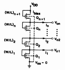
Figure 3.49. NMOS voltage divider.
3.2. Derive the formulas for the W/L ratios of Fig. 3.49 if the currents drawn at the nodes Vo1, Vo2, and Vo3 are not negligible.
3.3. Prove Eq. (3.7) for the circuit of Fig. 3.3.
3.4. Prove Eq. (3.25) for the circuit of Fig. 3.11.
3.5. In Figs. 3.10 and 3.11, assume that ro ![]() rd1 and gm2 = gm3. Show that the output resistance is increased by the open-circuit voltage gain of Q1.
rd1 and gm2 = gm3. Show that the output resistance is increased by the open-circuit voltage gain of Q1.
3.6. (a) Prove that Eq. (3.25) holds for the circuit of Fig. 3.12. (b) Analyze the circuit of Fig. 3.13. How much is rout? Show that the output resistance is that of Q2, magnified by the voltage gain of Q3.
3.7. Calculate the gain of the circuit of Fig. 3.23 without neglecting the rdi.
3.8. Prove Eqs. (3.56) and (3.57) for the circuit of Fig. 3.29.
3.9. Prove Eq. (3.64) for the circuit of Fig. 3.30.
3.10. (a) Derive the relations for vo,d and vo,c of the source-coupled stage (Fig. 3.38) if the circuit is not exactly symmetrical, (b) Rewrite your relations in the form

What are Add, Adc, and Acd, and Acc? (c) Let the maximum difference between symmetrically located elements in the small-signal equivalent circuit be 1%. How much are the maximum values of and |Acd| and |Adc|?
3.11. Derive Eq. (3.84) for the circuit of Fig. 42a. (Hint: Write and solve the current equations for nodes A, B, and C.)
3.12. Modify the CMOS differential stage of Fig. 3.42 so that it has differential output signals. Compare the differential gain with that of the original circuit!
3.13. Prove that the small-signal output impedance of the circuit of Fig. 3.43 is given by Eq. (3.89). (Hint: Write and solve the current law for nodes A, B, and C.)
3.14. Analyze the CMOS gain stage of Fig. 3.45 in the Laplace domain, (a) Find the exact transfer function Aν(s) from Fig. 3.45c. (b) Use Miller effect approximation to derive the simplified circuit of Fig. 3.45d; analyze the simplified circuit to verify Eq. (3.91).
3.15. Analyze the NMOS source follower of Fig. 3.47; verify Eq. (3.101).
3.16. Analyze the cascode gain stage of Fig. 3.46 in the Laplace transform domain, (a) Verify the equivalent circuits of Fig. 3.46b to d. (b) Show that Eq. (3.98) holds for the circuit of Fig. 3.46d.
REFERENCES
1. P. R. Gray and R. J. Meyer, Analysis and Design of Analog Integrated Circuits. Wiley, New York, 1993.
2. J. L. McCreary and P. R. Gray, IEEE J. Solid-State Circuits, SC-10(6), 371–379 (1975).
3. D. J. Hamilton and W. G. Howard, Basic Integrated Circuit Engineering, McGraw-Hill, New York, 1975.
4. T. C. Choi et al., IEEE J. Solid-State Circuits, SC-18(6), 652–664 (1983).
5. Y. Tsividis and P. Antognetti, Design of MOS VLSI Circuits for Telecommunications, Prentice Hall, Upper Saddle River, N. J., 1985.
6. P. R. Gray, Part II, IEEE Press, New York, 1980.
7. Y. Tsividis, IEEE J. Solid-State Circuits. SC-13(3), 383–391 (1978).
8. D. Senderowicz, D. A. Hodges, and P. R. Gray, IEEE J. Solid-State Circuits. SC-13(6), 760–766(1978).
9. K. Bult and G. J. Geelen, IEEE J. Solid-State Circuits, SC-25(6), 1379–1384 (1990).
10. E. Sackinger and W. Guggenbuhl, IEEE J. Solid-State Circuits SC-25(1). 289–298 (1990).
11. D. Allstot, IEEE J. Solid-State Circuits. SC-17(6), 1080–1087 (1984).