
CHAPTER 6
DIGITAL-TO-ANALOG CONVERTERS
The analog-to-digital (A/D) and digital-to-analog (D/A) converters are the main link between the analog signals and the digital world of signal processing. Data converters are generally divided into the two broad categories of Nyquist-rate and oversampling converters. Nyquist-rate converters are converters that operate at 1.5 to 5 times the Nyquist rate (i.e., a sample rate of 3 to 10 times the signal's bandwidth), and each input signal is uniquely represented by an output signal. Conversely, oversampling or delta-sigma converters operate at sampling rates that are much higher than the input signal's Nyquist rate and increase the output signal-to-noise ratio by subsequent filtering that removes the out-of-band quantization noise. The ratio of the sampling rate to the Nyquist rate is called the oversampling ratio. For most practical delta-sigma converters, the oversampling ratio is typically between 16 and 256.
A Nyquist-rate digital-to-analog converter (DAC) is a device that converts a digital input signal (or code) to an analog output voltage (or current) that is proportional to the digital signal. In this and the following chapters a variety of methods are presented for realizing Nyquist-rate converters. Oversampling converters are not discussed in this book; the interested reader is referred to Ref. 20 for an in-depth coverage of this subject. The chapter begins with a general introduction and characterization of the converters, followed by a discussion of voltage, charge, current, and hybrid-mode D/A converters.
6.1. DIGITAL-TO-ANALOG CONVERSION: BASIC PRINCIPLES
The block diagram of a D/A converter is shown in Fig. 6.1. The inputs are a reference voltage Vref and an N-bit digital word b1 b2 bN. Under ideal conditions, in the absence of noise and any imperfections, the D/A converter voltage output can be expressed as

Figure 6.1. Block diagram of a digital-to-analog converter.
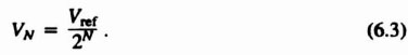
where N is the number of the bits of the input digital word. For an N-bit D/A converter the resolution is 2N and is equal to the number of discrete analog output levels corresponding to the various input digital codes. If Vref represents the input reference voltage, the smallest analog output corresponding to one least significant bit (LSB) is
For bipolar analog outputs, the digital input code retains the sign information in one extra bit—the sign bit—in the most significant bit (MSB) position. The most commonly used binary codes in bipolar conversion are sign magnitude, one's complement, offset binary, and two's complement. Table 6.1 shows each of the bipolar codes for a 4-bit (3-bit plus sign) digital word. The word length N determines the range of the numbers associated with each of the four binary representation systems. In all four notations, the largest positive number is given by 1 − 2−(N−1) in decimal. For sign-magnitude and one's complement numbers, the lower bound is −[1 − 2−(N − 1)] while in two's complement and offset binary the most negative number is −[1 − 2−(N−1)]. All four number systems have unique representations for all numbers except for the zero in sign-magnitude or one's complement notations. Positive and negative zeros have different representations in these two number systems. For two's complement and offset binary notations there is a unique zero representation.
The most useful way of indicating the relationship between analog and digital quantities involved in a conversion is the input-output transfer characteristic. Figure 6.2 shows the transfer characteristic for an ideal 3-bit unipolar D/A converter that is made up of 23 distinct output levels. In practical D/A converters the ideal transfer characteristic of Fig. 6.2 cannot be achieved. The types of errors or deviations from this ideal condition are graphically illustrated in Fig. 6.3. The offset error is illustrated in Fig. 6.3a and is defined as the deviation of the actual output from the ideal output when the ideal output should be zero. The gain error is the change in the slope of the transfer characteristic and is shown in Fig. 6.3b. The gain error is due to the inaccuracy of the scale factor or the reference voltage. The linearity is a measure of the nonlinearity error at the output, after the offset and gain errors have been removed. There are two types of nonlinearity errors. Integral nonlinearity (INL) is defined as the worst-case deviation of the transfer characteristic from an ideal straight line between zero and full scale (i.e., the endpoints of the transfer characteristic). The differential nonlinearity (DNL) is the maximum deviation of each output step size of 1 LSB. It is a measure of the nonuniform step sizes between adjacent transitions and is normally specified as a fraction of LSB. The integral and differential nonlinearities are shown in Fig. 6.3c. Unlike the offset and gain errors, the nonlinearity errors cannot be corrected by simple trimming and they can only be minimized by improving the matching of the precision components of the D/A converters (i.e., resistors or capacitors). Finally, monotonicity in a D/A converter implies that the analog output always increases as the digital input code increases. Nonmonotonicity is due to excessive differential nonlinearity. Guaranteed monotonicity implies that the maximum differential nonlinearity is less than one LSB. Nonmonotonicity is illustrated in Fig. 6.3c, where the analog output decreases at some points in its dynamic range while the input code is increasing.
TABLE 6.1. Commonly Used Bipolar Codes

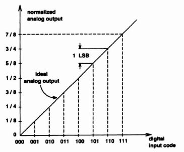
Figure 6.2. Ideal conversion relationship in a 3-bit D/A converter.


Figure 6.3. Graphic illustration of various errors present in a D/A converter: (a) offset error; (b) gain error. (c) differential nonlinearity, integral nonlinearity, and nonmonotonic response.
6.2. VOLTAGE-MODE D/A CONVERTER STAGES
An important, yet simple class of D/A converters is based on the accurate scaling of a reference voltage Vref. Voltage scaling can be achieved by connecting a series of N equal segments of resistors between Vref and ground. For an N-bit converter the resistor string consists of 2N segments. The string of resistors behave as a voltage divider and the voltage across each segment is one LSB, given by
An N-bit D/A converter can be realized by using a string of 2s resistors and a switching matrix implement with MOS switches [1]. The D/A conversion technique is illustrated with a conceptual 3-bit version of the unipolar converter shown in Fig. 6.4. Here the switch matrix is connected in a treelike manner, which eliminates the need for a digital decoder. For an N-bit converter, 2N+1 − 2 switches are needed. As illustrated in Fig. 6.4, the voltage selected propagates through N levels of switches before getting to the buffer amplifier. The buffer is necessary to provide a low-impedance output to the external load. Assuming that the buffer's dc offset voltage does not vary with its input common-mode voltage, the D/A technique has guaranteed monotonicity and can be used for converters up to 10-bit resolution. As the number of the bits increases, the delay through the switch network imposes a major limitation on the speed. The output impedance of the resistor string also varies, as a function of the closed switch position in the network. Also, the delay through the resistor string may become a major source of delay.

Figure 6.4. Three-bit unipolar resistive DAC with 23 resistors and transmission gate tree decoder.

Figure 6.5. Three-bit unipolar resistive DAC with 23 resistors and digital decoder.
For high-speed applications the tree decoder is replaced with a digital decoder. One such 3-bit DAC is shown in Fig. 6.5. The logic circuit is an N-to-2N decoder that can take a large area. The common node of all switches is directly connected to the buffer amplifier. The 2N junctions of the transistors have a large area and result in a large capacitive load. The voltage selected propagates through one switch; hence, despite the larger capacitive load, the DAC output can achieve higher-speed operation.
A more efficient implementation of a 5-bit resistor DAC is shown in Fig. 6.6. This method, known as the intermeshed ladder architecture, uses a two-level row-column decoding scheme similar to one used in digital memon [2–4]. The N-to-2N decoding is achieved by splitting N to N1 + N2 = N and realizing it as the combination of an ![]() row and
row and ![]() column decoders. For a given digital code, one of the
column decoders. For a given digital code, one of the ![]() columns is selected, all transistor switches in that column are turned on, and the
columns is selected, all transistor switches in that column are turned on, and the ![]() resistor nodes are connected to
resistor nodes are connected to ![]() rows. The row decoder selects one of the
rows. The row decoder selects one of the ![]() rows and connects it to the input of the buffer amplifier.
rows and connects it to the input of the buffer amplifier.

Figure 6.6. Five-bit intermeshed-ladder architecture resistive DAC.
This approach uses ![]() subsegments, each consisting of
subsegments, each consisting of ![]() resistor segments. For large N the number of the resistors, 2N, grows exponentially and the impedance of the resistor array becomes very large. The output impedance also varies as a function of the position of the closed switch in the network. To reduce the impedance of the array and hence its settling time, a coarse array is placed in parallel to the fine one. The coarse array consists of
resistor segments. For large N the number of the resistors, 2N, grows exponentially and the impedance of the resistor array becomes very large. The output impedance also varies as a function of the position of the closed switch in the network. To reduce the impedance of the array and hence its settling time, a coarse array is placed in parallel to the fine one. The coarse array consists of ![]() (N1, is the number of the rows) resistors and is denoted by Rc in Fig. 6.6. The coarse array in this way determines
(N1, is the number of the rows) resistors and is denoted by Rc in Fig. 6.6. The coarse array in this way determines ![]() accurate voltages and determines the value corresponding to the N1 MSBs. In this arrangement the
accurate voltages and determines the value corresponding to the N1 MSBs. In this arrangement the ![]() resistor subsegments each consist of
resistor subsegments each consist of ![]() segments, and the endpoints of the subsegments are connected to the
segments, and the endpoints of the subsegments are connected to the ![]() coarse resistors. If the coarse resistors are represented by Rc and the resistors in the subsegment by Rf, the total resistance of the array is given by
coarse resistors. If the coarse resistors are represented by Rc and the resistors in the subsegment by Rf, the total resistance of the array is given by
As a result of this modification, the worst-case output resistance of the array seen by the buffer is reduced to Rarray/4.
For high-resolution applications the resistor string DAC suffers from several drawbacks: The number of the resistors and switches grows exponentially and it exhibits a long delay at the output. Hence the resistive DACs of Figs. 6.4 to 6.6 are not practical when the number of the bits grows beyond 10. To take advantage of the inherent monotonicity of the voltage-division DAC while keeping the number of resistors to a manageable level, it is possible to use a two-stage DAC such as the one shown in Fig. 6.7 [5], As the figure shows, the 6-bit DAC consists of two resistor strings each having eight segments. The coarse resistor string is connected between Vref and ground. Two operational amplifiers connected as voltage followers buffer consecutive voltages of the coarse DAC. The fine resistor string is connected between the two outputs of the followers. The monotonocity of the two-stage DAC cannot be guaranteed, due to the offset voltage of the unity-gain buffers. A special sequence can be used to operate the coarse array switches to make the operation of the DAC independent of the buffer offset voltages. To understand this, consider a portion of the coarse array shown in Fig. 6.8. This figure corresponds to the ith code of the coarse bits, where buffer 1 is connected to segment voltage Vi and buffer 2 to segment voltage Vi−. The output of the buffers will be (V1)i − Voff1, and (V2)i = Vi−1 − Voff2 are the corresponding offset voltages of the first and second op-amps. For the next sequential code, if node A moves to Vi + 1 and node B to Vi, the buffer outputs will be (V1)i + 1 = Vi + 1 − Voff1 and (V2)i + 1 = Vi − Voff2. For monotonic operation it is necessary for (V2)i+1 = (V1)i; otherwise, the consecutive coarse output voltages will not be continuous. This is possible only if Voff1 = Voff2 or Voff1 = Voff2 = 0, which cannot be guaranteed in practice. Alternatively, for the sequential code, node A can be kept at Vi and node B switched to Vi+1. This choice guarantees a continuous output from the coarse array and hence monotonic operation for the DAC. However, since the top and bottom of the fine resistor string switches for consecutive codes, the decoding and switching of the fine DAC should be modified accordingly. Figure 6.9 shows the complete circuit diagram of the 6-bit DAC, which includes the switching details of the coarse and fine DACs. As the figure shows, for an N-bit DAC, the converter functions by applying voltage Vref to the top of the coarse resistor array and dividing it to 2N/2 nominally equal voltage segments. For a given code, buffer A1 transfers the voltage at the ith tap to the top of the fine string, while A2 applies the voltage at tap i − 1 to the bottom of fine string. The A3 output results from linearly interpolating the voltage drop between taps i and i − 1, weighted by the N/2 lower bits of the N-bit input digital word. For the next coarse digital code, the polarity of the voltage across the fine resistor string is reversed. This reversal occurs at every other adjacent resistor segment and is corrected in the second stage by alternating between two switch arrays. The least significant bit of the digital input code of the coarse DAC makes this selection. This bit selects between the odd and even segments, which allows the analog output of the coarse divider to have a continuous output voltage independent of the offset of the two voltage followers. By using this method it is possible to obtain a 16-bit DAC which has a guaranteed monotonicity without the need for a straight 216-segment resistor divider.

Figure 6.7. Two-stage 6-bil resistor divider DAC.
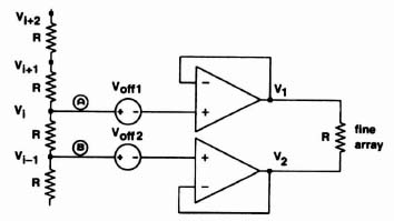
Figure 6.8. Portion of the coarse resistor segment.
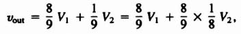
For an N-bit DAC, the circuit of Fig. 6.9 uses two 2N/2-segment resistor strings, two N/2-to-2N/2 decoders, and four sets of switching elements. Alternatively, the two-stage DAC can be implemented using a single segment resistor string, two sets of switching elements, and two N/2-to-2N/2 decoders. A 6-bit version of such a DAC is shown in Fig. 6.10. Here the two inputs of the A1 and A2 buffers are independently switched to the taps of the eight-segment resistor string. The three MSBs of the input digital word are decoded to eight lines that control the connection of A1 to the taps of the resistor string. The next three LSBs control the connection of A2 to the resistor string in a similar fashion. A nine-segment resistor string is placed between the outputs of A1 and A2. Tap 8, from the bottom of the string, is buffered by A3 and brought out as the output of the DAC. From Fig. 6.10, V1, and V2 are the outputs of two independently controlled 3-bit DACs. One converts the three MSBs and the other the three LSBs of the input digital word to analog voltages. Ignoring the dc offset voltages of the three op-amps, νout, can be calculated as

Figure 6.9. Detailed circuit diagram of two-stage monotonic voltage-divider DAC.

Figure 6.10. Alternative form of 6-bit unipolar two-stage rcsistive-divider DAC.
or
so that

Ignoring the factor ![]() , the relationship inside the parentheses represents the output of a 6-bit segmented DAC. If the effect of the op-amp offsets is included in the calculations, Eq. (6.5) will be modified in the following way:
, the relationship inside the parentheses represents the output of a 6-bit segmented DAC. If the effect of the op-amp offsets is included in the calculations, Eq. (6.5) will be modified in the following way:

As Eq. (6.6) shows, the dc offset of the op-amps appears as a constant dc voltage at the output without interfering with the DAC operation. Therefore, if the op-amp offset voltages do not change with the common-mode voltage, this structure is inherently monotonic and the complex switching scheme of the DAC shown in Fig. 6.9 will not be necessary. The only disadvantage of this scheme is the ![]() attenuation factor for the 6-bit DAC. For an N-bit DAC, if we split the input code into two N/2 bits (N is even) segments, the output relationship will be given by
attenuation factor for the 6-bit DAC. For an N-bit DAC, if we split the input code into two N/2 bits (N is even) segments, the output relationship will be given by

As an example for a 16-bit DAC, N = 16 and we have

The first stage will be an 8-bit DAC followed by two buffer amplifiers with a 257-segment resistor string connected between their outputs. The final 16-bit DAC output will be taken from tap 256 of the second-stage resistor string. The 256/257 attenuation can be ignored or compensated by modifying the reference voltage, Vref, which is connected to the top of the first-stage resistor string.

Figure 6.11. Offset-compensated switched-capacitor sample-and-hold circuit.
The DACs described so far in this section all use unity-gain buffers to isolate the resistor string from the external load. The unity-gain buffer has several disadvantages. For high-resolution DACs, the op-amp should have a large common-mode-rejection ratio (CMRR) to maintain the accuracy over the entire input commonmode range. Also, for low-voltage operation, complex op-amps with rail-to-rail input stage should be used to facilitate operation over the wide input range. For bipolar outputs, the bottom of the resistor string will be connected to a negative reference. The absolute values of the positive and negative reference voltages should match closely. Any mismatch will introduce an offset and linearity error.
An alternative to the unity-gain buffer is the offset-compensated switched-capacitor sample-and-hold stage shown in Fig. 6.11, where ![]() 1 and
1 and ![]() 2 are nonoverlapping two-phase clocks [6]. When
2 are nonoverlapping two-phase clocks [6]. When ![]() 1 is high, capacitor C will be charged between the output of the DAC and the op-amp offset voltage and acquires the voltage νin − Voff, where νin = Vdac. When
1 is high, capacitor C will be charged between the output of the DAC and the op-amp offset voltage and acquires the voltage νin − Voff, where νin = Vdac. When ![]() 2 goes high, the output becomes VDAC − Voff + Voff = VDAC, which is independent of the op-amp offset voltage.
2 goes high, the output becomes VDAC − Voff + Voff = VDAC, which is independent of the op-amp offset voltage.
It is also possible to use the switched-capacitor gain stage shown in Fig. 6.12a as a buffer [7,8]. In this circuit, when ![]() 1 = “1,” the op-amp has its inverting input terminal shorted to its output node and hence performs as a unity-gain voltage follower with output voltage Voff. Hence capacitor αC recharges to Voff − νin while C changes to Voff. When next
1 = “1,” the op-amp has its inverting input terminal shorted to its output node and hence performs as a unity-gain voltage follower with output voltage Voff. Hence capacitor αC recharges to Voff − νin while C changes to Voff. When next ![]() 2 goes high, αC recharges to Voff and C to Voff − νoff. If the time when this happens is t = NT, by charge conservation at node A,
2 goes high, αC recharges to Voff and C to Voff − νoff. If the time when this happens is t = NT, by charge conservation at node A,

In this equation, Voff terms cancel out and νout(nT) = ανin(nT − T/2) results. Thus a positive gain of α and a delay T/2 are provided by the stage, and the output offset voltage is Vos = 0. Note also that the circuits of Figs. 6.11 and 6.12 are fully stray insensitive.
By interchanging the clock phases at the input terminals, an inverting voltage amplifier can also be obtained (Fig. 6.13). By an analysis similar to that performed for the circuit of Fig. 6.12, it can be shown (Problem 6.3) that this circuit is a delay-free inverting amplifier with gain α. As before, Voff is canceled by the switching arrangement and does not enter νoff, if the op-amp gain is infinite. (See Problem 6.3 for the finite-gain case.)
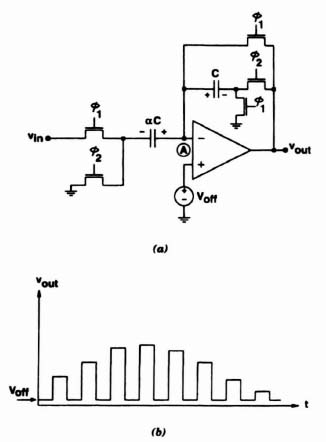
Figure 6.12. Offset-compensated noninverting voltage amplifier: (a) circuit; (b) output waveform.

Figure 6.13. Offset-compensated inverting voltage amplifier.
As mentioned earlier, in the circuits of Figs. 6.11, 6.12, and 6.13, the output voltage is Voff whenever ![]() 1 is high, hence the output is valid only when
1 is high, hence the output is valid only when ![]() 2 is high. As an example, for the circuit of Fig. 6.12a, the output waveform is as illustrated schematically in Fig. 6.12b. Clearly, the op-amp must have a high slew rate and fast settling time, especially if the clock rate is high. At the cost of a few additional components [9], this disadvantage of offset compensation can be eliminated (Problem 6.4).
2 is high. As an example, for the circuit of Fig. 6.12a, the output waveform is as illustrated schematically in Fig. 6.12b. Clearly, the op-amp must have a high slew rate and fast settling time, especially if the clock rate is high. At the cost of a few additional components [9], this disadvantage of offset compensation can be eliminated (Problem 6.4).
Low-frequency noise signals, which do not change substantially during clock period T, are similarly canceled by offset compensation. Thus the troublesome 1/f noise discussed in Section 2.7 is greatly reduced. Figure 6.14a and b illustrate the output noise spectra with and without offset compensation, respectively. Note that cancellation also occurs at 2/fc, 4/fc,…., which are equivalent to dc for the sampled noise.
If the digital input signal is bipolar, that is, if it has either a positive or a negative sign as indicated by a sign bit b0, the gain stage with polarity control shown in Fig. 6.15 can be used. When b0 = 0, indicating that the digital signal is positive, the circuit functions like the noninverting unity-gain sample-and-hold stage of Fig. 6.12. If b0 = 1. the digital signal is negative; then the roles of ![]() 1 and
1 and ![]() 2 interchange in the input branch and the circuit functions like the inverting unity-gain stage of Fig. 6.13. The advantages of using the switched-capacitor stages of Figs. 6.11 to 6.15 are that the op-amp has no common-mode input signal, and bipolar outputs can be generated from a unipolar DAC with a single positive (or negative) reference voltage.
2 interchange in the input branch and the circuit functions like the inverting unity-gain stage of Fig. 6.13. The advantages of using the switched-capacitor stages of Figs. 6.11 to 6.15 are that the op-amp has no common-mode input signal, and bipolar outputs can be generated from a unipolar DAC with a single positive (or negative) reference voltage.
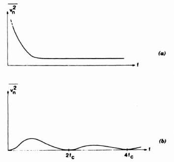
Figure 6.14. Noise power for a switched-capacitor voltage amplifier: (a) without offset compensation; (b) with offset compensation.
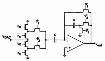
Figure 6.15. Offset-compensated switched-capacilor gain stage with polarity control.
6.3. CHARGE-MODE D/A CONVERTER STAGES
An important advantage of switched-capacitor circuits is that they can be made digitally variable and thus also programmable. This is accomplished by replacing some capacitors in the circuit by programmable capacitor arrays (PCAs). Such a binary-programmed array [10] is shown in Fig. 6.16. In the figure the triangular symbols denote inverters, and b0, b1…, b7, are binary-coded (high or low, 1 or 0) digital signals. Thus if (say) b7 is high, the left-side switching transistor associated with capacitor C is on and the right-side transistor is off. Hence C is connected between nodes X and X′. If b7 is low, the right-side transistor is on, and it connects the right-side terminal of C to ground rather than to X′. Therefore, C never floats, and the total capacitance loading at node X is constant. The value of the capacitance between X and X′ in the 8-bit PCA of Fig. 6.16 is thus clearly

while the total capacitance loading node X is 2C(1 − 2−8) (Problem 6.5).
Care must be taken in the design of the PCA to minimize noise injection from the substrate into the circuit. Thus the bottom plate of the capacitor (which is in the substrate or right above it) should never be connected to the inverting input terminal of an op-amp; otherwise, the noise from the power supply which biases the substrate will be coupled to the op-amp's input and amplified by the op-amp.
An obvious application of PCAs is the realization of charge-mode D/A converters. It can be obtained by replacing the input capacitance αC in the offset-free voltage amplifier of Fig. 6.12a by a PCA. An example of an N-bit charge mode DAC is shown in Fig. 6.17, where Vref is a temperature-stabilized constant reference voltage. If b1, represents the most significant bit (MSB) and bN the least significant bit (LSB), the output voltage at the end of clock period ![]() 2 is given by
2 is given by

Thus the output is the product of the reference voltage Vref and the binary-coded digital signal (b1, b2, b3,…, bN).
Note that the orientation of all capacitors is such that their top plates (indicated by light lines) are connected to the op-amp input terminal. This reduces substrate noise voltage injection. Also, due to the presence of the switching devices driven by ![]() ,
, ![]() , and so on, the total capacitance connected to the op-amp input is constant, which makes its compensation an easier task.
, and so on, the total capacitance connected to the op-amp input is constant, which makes its compensation an easier task.

Figure 6.16. Binary-programmable capacitor array (PeA).

Figure 6.17. An n-bit charge-modedigital-to-analog converter.
If the digital input signal is bipolar, that is, if it has either a positive or a negative sign as indicated by a sign bit b0, the DAC shown in Fig. 6.18 can be used. If b0 = 0, indicating that the digital signal is positive, the circuit functions in exactly the same way as the DAC of Fig. 6.17. If, however, b0 = 1, so that the digital signal is negative (as can easily be deduced), in the input branch ![]() 1 and
1 and ![]() 2 exchange roles. Now the circuit functions as the inverting voltage amplifier of Fig. 6.13. Thus the input-output relation is
2 exchange roles. Now the circuit functions as the inverting voltage amplifier of Fig. 6.13. Thus the input-output relation is

as required by the negative digital signal.
For an N-bit DAC, the capacitor ratio is 2N and the total capacitance Ctotal = (2N+1 − 1)C. For N = 8, 28 = 256 and Ctotal = 511C. The ratio and the total capacitance increase rapidly with increasing N and the matching accuracy deteriorates. The offset-free scheme of Fig. 6.18 can be used in a cascade design to reduce the capacitor ratio [11]. The circuit diagram for a bipolar 8-bit D/A converter is shown in Fig. 6.19. The output of the first stage is fed to the second stage with the same weighting as the least significant bit. The output voltage at the end of clock period ![]() 2 is given by
2 is given by

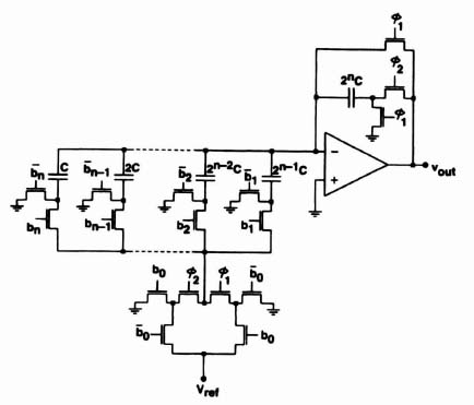
Figure 6.18. DAC with bipolar output.
which reduces to

where k is determined by the sign of b1. The capacitor ratio is reduced to 24 = 16 and the total capacitance is Ctotal = 63C. As Fig. 6.19 shows, the capacitor ratio is reduced without increasing the conversion cycles. For an N-bit (N-even) bipolar D/A converter, the capacitor ratio is 2N/2 and the total capacitance Ctotal = [2(N/2 + 2) − 1]C, which corresponds to an improvement of 2N/2 − 1 over the direct method. The circuit is compatible with most process technologies and uses a single reference voltage for bipolar outputs.
6.4. HYBRID D/A CONVERTER STAGES
In the cascaded D/A converter shown in Fig. 6.19, the voltage corresponding to the LSBs propagates through two op-amps before reaching the output. The settling time of the two cascaded op-amp stages sets an upper limit on the maximum conversion speed. A more effective way to reduce component spread and achieve high precision is to combine the charge-mode and resistor-divider-mode DACs described earlier in the chapter. The most straightforward combination is to replace the LSB stage (first stage) of the cascaded D/A converter of Fig. 6.19 with one of the resistor-divider DACs of Fig. 6.5 or 6.6. One example of this approach is shown in Fig. 6.20, where a 7-bit bipolar-output DAC is realized as the cascade of a 3-bit charge-mode DAC and a 3-bit resistor divider-mode DAC. The MSB in this case is the sign bit and controls the polarity of the output. For a 16-bit unipolar DAC an 8-bit charge-mode DAC and an 8-bit resistor divider-mode DAC can be used. In this approach the LSBs are used to program the output of the resistor DAC while the MSBs control the capacitor array. The overall accuracy is determined largely by the MSB DAC. Monotonicity cannot be guaranteed because the charge-mode DAC is not accurate within one LSB of the overall DAC.
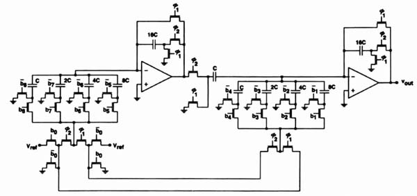
Figure 6.19. Circuit diagram of a bipolar output 8-bit cascaded D/A converter.

Figure 6.20. Seven-bit hybrid DAC stage with charge MSB and voltage-divider LSB DACs.

Figure 6.21. Six-bit hybrid unipolar DAC stage with resistor-divider MSB and charge LSB DACs.
For inherently monotonic design, a two-stage approach can be used where the MSBs are used to program a resistor-divider DAC and the LSBs control a binary-weighted programmable capacitor array (PCA) [12]. This approach is similar to the one used in an inherently monotonic successive-approximation A/D converter [13]. A 6-bit two-stage unipolar D/A converter is shown in Fig. 6.21. For a 7-bit bipolar DAC, a sign bit can be added to control the clock phases of the switched-capacitor gain stage. The overall DAC consists of a 3-bit resistor-divider DAC and a 3-bit charge-mode DAC. The three MSB connect adjacent nodes of the resistor string to the two high (bus-H) and low (bus-L) buses. The three LSBs connect the binary-weighted capacitor array to the high and low buses through the two switches controlled by ![]() 1 and
1 and ![]() 2. If an LSB is a “1,” the corresponding capacitor is connected to the high bus (bus-H); if the bit is “0” it is connected to the low bus (bus-L). For a positive output, when
2. If an LSB is a “1,” the corresponding capacitor is connected to the high bus (bus-H); if the bit is “0” it is connected to the low bus (bus-L). For a positive output, when ![]() 1, is high, the bottom plates of the binary-weighted capacitor are connected to bus-H or bus-L. When
1, is high, the bottom plates of the binary-weighted capacitor are connected to bus-H or bus-L. When ![]() 1 goes low and
1 goes low and ![]() 2 goes high, the bottom plates of the capacitors switch to ground and a voltage corresponding to the digital code appears at the output of the gain stage. If a sign bit is used to control the sequence of the clock phases, a positive or negative output will be generated at the output of the DAC. The absolute accuracy and linearity of the entire DAC are limited by the accuracy of the voltage division of the resistor string. The monotonicity of the entire DAC is guaranteed as long as the capacitor array is monotonic. For a 16-bit bipolar output DAC, an 8-bit resistor DAC and a 7-bit capacitor DAC can be used. The sign bit will control the polarity of the output.
2 goes high, the bottom plates of the capacitors switch to ground and a voltage corresponding to the digital code appears at the output of the gain stage. If a sign bit is used to control the sequence of the clock phases, a positive or negative output will be generated at the output of the DAC. The absolute accuracy and linearity of the entire DAC are limited by the accuracy of the voltage division of the resistor string. The monotonicity of the entire DAC is guaranteed as long as the capacitor array is monotonic. For a 16-bit bipolar output DAC, an 8-bit resistor DAC and a 7-bit capacitor DAC can be used. The sign bit will control the polarity of the output.
6.5. CURRENT-MODE D/A CONVERTER STAGES
All current-mode DACs are made of three basic blocks: a current reference generator, a controlled current switching matrix, and a current-to-voltage converter. The current reference generator is simply a voltage-to-current converter. One such circuit is shown in Fig. 6.22, where a reference voltage and resistor is used to generate the reference current. For the circuit of Fig. 6.22, the op-amp forces the voltage across the reference resistor to Vref. So the reference current is given by
The diode-connected p-channel device Q1 generates a gate-to-source voltage that can be used as bias voltage to mirror the reference current into the current-switching matrix. The current-switching matrix under the control of the N-bit digital input code produces an output given by
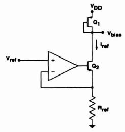
Figure 6.22. Current reference generator for the current DAC.
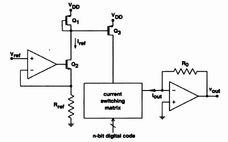
Figure 6.23. Simplified block diagram of a current-mode DAC.
where b1 is the MSB and bN the LSB.
The output current, Iout flows into the current-to-voltage converter, which in its simplest form is a resistor. To provide a low-impedance output, an op-amp should be used. In this case the current-to-voltage converter is an op-amp with a feedback resistor. The simplified block diagram of a current-mode DAC is shown in Fig. 6.23, where the output νout, is given by

One of the main applications of high-speed current-mode D/A converters is in raster-scan graphics monitors, which are used in most computer systems. High-speed DACs are also used in digital and high-definition television. These systems normally include three 8-bit high-speed DACs for red, green, and blue colors. In today's high-resolution color monitors, each DAC operates at speeds in excess of 200 MHz and is designed to have a current output that drives a 75-Ω doubly terminated line [14,15].
The basic architecture of a 3-bit current DAC is shown in Fig. 6.24. The DAC consists of 23 − 1 = 7 identical current sources, where each current source, under the control of the input code, can switch between the output load and ground. For an inherently monotonic DAC with good differential nonlinearity (DNL), a thermometer-type decoder must be used. A 3-bit thermometer decoder converts the input 3 bits to 23 − 1 = 7 output bits, where the number of l's in the output code is equal to the decimal value of the binary code. Table 6.2 presents the truth table of a 3-bit thermometer-code decoder. If d0 to d6 are used to control the current sources of Fig. 6.24, then moving from one code to the next, one additional current source is turned on, which increases the total output current, hence guaranteeing monotonicity. The thermometer-decoding scheme also improves the glitch performance. A glitch occurs when, say, going from 3I0 to 4I0, for the output current, one set of three current sources turn off and another set of four current sources turn on. Any delay between turning the two groups on and off will result in a positive or negative glitch. This phenomenon is common in a binary-weighted current source DAC. In a thermometer decoder DAC, going from 3I0 to 4I0, the three current sources that supply 3I0 remain on and a fourth turns on to supply 4I0, eliminating any glitches.

Figure 6.24. Three-bit current DAC using a thermometer decoder
TABLE 6.2. Truth Table for 3-Bit Thermometer Decoder

As the number of bits increase, straight thermometer decoding becomes impractical. For more efficient implementation, a two-dimensional row–column decoding scheme can be used. For example, for a 6-bit DAC, a 3-bit row and 3-bit column decoder can be used. The DAC will consist of 26 − l = 63 identical current sources arranged as a matrix. Figure 6.25 shows the basic architecture of the 6-bit DAC. For example, if the digital value for the 6-bit input code corresponds to a decimal number of 30, thirty current sources in the matrix are turned on and these outputs are summed to form the output current. In Fig. 6.25 the matrix consists of three types of rows: (1) rows in which all current cells are turned on, (2) rows in which all the current cells are turned off, and (3) a row in which the cells are partially turned on. Based on the three types of rows and the outputs of the row and column decoders, a logic is designed to control the individual current cells [14].
The architecture of Fig. 6.25 is such that in the actual physical layout of the DAC, the control logic for each cell should be placed next to the current source. This requirement puts a limitation on the matching accuracy of the current cells and hence the linearity of the DAC. The architecture of the DAC can be greatly simplified if a slightly different decoding scheme is used. The block diagram of the simplified 6-bit DAC is shown in Fig. 6.26. It consists of one row of seven current cells and seven rows of eight current cells. The output of the column decoder controls the individual cells in the first row, and the seven outputs of the row decoder each control an entire row. In this arrangement, for a digital code corresponding to a decimal value of 30, three entire rows and six cells in the first row will turn on. As we increment the input digital code, the current cells of the first row turn on sequentially. When all seven current cells are turned on, one more increment will turn off all seven cells in the first row and turn on one entire row of eight current cells. Turning off one set of seven devices and turning on another set of eight devices may cause a slight glitch. Also, the architecture in not inherently monotonic. However, for a 6-bit DAC, monotonicity can be guaranteed as long as the DAC is 3-bit accurate. The physical layout of the DAC is very straightforward, however. Since the outputs of the thermometer decoders control the current cells directly, no additional logic is necessary and all current cells can be placed next to each other, improving the matching and hence the accuracy of the DAC.

Figure 6.25. Six-bit current DAC architecture.
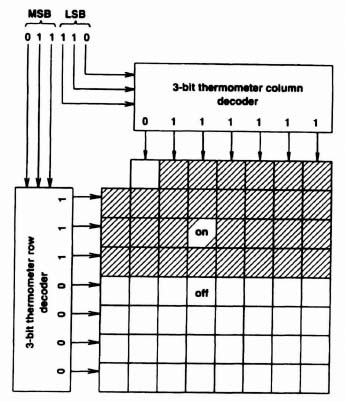
Figure 6.26. Simplified 6-bit current DAC architecture.
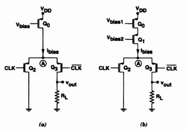
Figure 6.27. Configuration of current source: (a) single transistor configuration; (b) cascade configuration.
The individual current switch is shown in Fig. 6.21a. The gate of Q0 is tied to a bias voltage such as the one shown in Fig. 6.22 and establishes the bias current. When the Clk signal is high Q2 is off, Q3 is on, and Ibias flows into the output load. When Clk goes low, Q3 turns off, Q2 turns on, and Ibias flows into ground. As shown in Fig. 6.27a, when the current flows into the load, the output voltage, νout modifies the voltage of node A, hence changing the drain-to-source voltage of Q0 and consequently, the bias current. To increase the output impedance of the current source, the cascode-connected current mirror shown in Fig. 6.27b can be used. The output voltage swing of the current source can be improved by using the modified biasing schemes discussed in Chapter 3.
An alternative current switch with improved current regulation is shown in Fig. 6.28 [16]. In this circuit the gate of transistor Q3 is not switched but is tied to a constant voltage Vdc. This stage is essentially a fully switched differential pair. The current Ibias is steered either to ground or to the output load, depending on the polarity of the digital input signal that is applied to the gate of Q2. In this circuit the potential of node A is independent of the potential of νout and is determined by the bias voltage Vdc, the bias current, and the VGS drop of Q3. Since the drain-to-source voltage of Q0 remains constant and independent of the output voltage, its drain current also remains unchanged. The simplified schematic of the voltage-to-current converter and the current switch is shown in Fig. 6.29 [17]. The transistor Qb1 is inserted in the feedback of the voltage-to-current converter to balance the drain-to-source voltage of all the current mirror transistors, hence equalizing their currents. Current output D/A converters using these types of switches exhibit very rapid settling times, typically on the order of 5 to 10 ns.
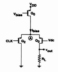
Figure 6.28. Configuration of improved current switch.
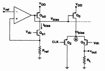
Figure 6.29. Current switch with a voltage-to-current converter.
6.6. SEGMENTED CURRENT-MODE D/A CONVERTER STAGES
For high-resolution current-mode DACs, the methods described in Section 6.5 are not practical because the number of current elements rises exponentially and the silicon area necessary to implement the DAC becomes excessively large. A more efficient method of implementing high-resolution current DACs, similar to the voltage mode, is the segmented approach [18]. Figure 6.30 shows the basic block diagram of an N-bit segmented D/A converter. An array of M equal coarse current sources (Iu) is shown. One of the coarse current sources can be divided into more fine current levels by a passive current divider. Controlled by the value of the input digital code, a number of the coarse and fine currents are switched to the output terminal, and the remaining currents are dumped to signal ground. In the circuit of Fig. 6.30, a thermometer decoder that decodes the N1 MSBs of the input code controls the coarse current sources. The fine current sources will be controlled by the remaining N − N1 LSBs. In this approach, use of the thermometer decoder guarantees monotonicity for the coarse current sources. The entire DAC is not inherently monotonic, however, because the last current source, which is divided into the fine currents, should match the other coarse current sources within one LSB of accuracy. To guarantee monotonicity, a three-way switch can be added to each coarse current source. For each code, the first m − 1 coarse current units are switched to the output, and coarse current unit number m is switched to the fine current divider. This method guarantees monotonic operation because the segment current selected, which is applied to the fine current divider, depends on the data input. Figure 6.31 shows the basic block diagram of an N-bit D/A converter. The N-bit input digital code is divided into C-bit coarse (MSBs) and F-bit fine (LSBs) codes. The C-bit MSBs are decoded by a binary-to-thermometer decoder that controls the coarse current sources. The remaining F bits directly control a binary-weighted current divider. The C coarse bits represent values from zero to 2C − 1. Therefore, 2C unit coarse current sources are required, including one for the segmentation current. Figure 6.32 shows the output current of the converter as a function of the input code. Assume that point A on the graph represents the analog value corresponding to the input digital word. The unit coarse current sources 1 through m − 1 (of 2C available unit current sources) are switched to the output line (I0,coarse) controlled by the MSBs, while the unit current source m denoted by Iseg, is divided into the fine current levels by a binary-weighted current divider and is switched to the output current line controlled by the LSBs. The output currents of the coarse network and fine current divider are added to form the total output current, expressed as
where Df represents the decimal value corresponding to the F LSBs and Iu is the unit coarse current source. An example of a 7-bit segmented DAC is shown in Fig. 6.33 where C = 3 and F = 4. There are a total of 23 = 8 unit coarse currents and a 4-bit binary-weighted divider. The reference voltage Vref1 is used to bias the unit coarse current transistors Q1 to Q8. The binary-to-thermometer decoder outputs control the gates of the three-way p-type MOS switches Q9 to Q32 that operate in the linear region. Cascode devices Q33 to Q48 are added to improve the accuracy of the coarse currents. This is achieved by equalizing the potentials of the switches and the segment current line, Iseg, which is connected to the 4-bit binary-weighted current divider. The basic current divider consists of 16 equal-sized common-gate and common-source transistors to Qf1. The individual drains are combined in binary-weighted numbers, 1, 2, 4, and 8. The output current is controlled by a two-way switch, which consists of p-type MOS transistors Qf17 to Qf24 The four LSBs directly control the gates of these transistors.

Figure 6.30. Basic block diagram of a segmented D/A converter.
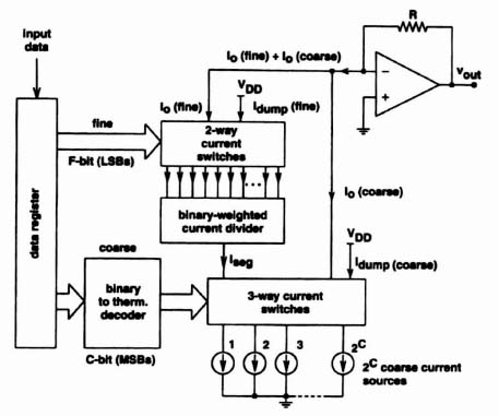
Figure 6.31. Basic block diagram of a segmented N-bit inherently monotonic current DAC.
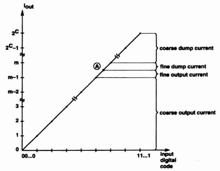
Figure 6.32. Segmented D/A output current as a function of input code.

Figure 6.33. Seven-bit segmented current DAC.
The accuracy of the segmented DAC is determined largely by the matching of the coarse unit current elements. Symmetrical layout techniques for the MOS transistors of the coarse current sources can improve the accuracy. However, the achievable precision based upon matching of components in a standard process is not sufficient. Therefore, additional calibration techniques are used to achieve high-resolution converters. Use of dynamically matched current sources is one of the self-calibration techniques that can be applied to the segmented current DAC of Fig. 6.30 to achieve well-matched current sources and hence a high-precision D/A converter [19]. To accomplish this, each unit coarse current source in Fig. 6.30 is continuously calibrated by a reference current Iref in such a way that all coarse elements are matched precisely. Before describing the complete process, the calibration principle for one single current source will be explained.
The basic calibrated current cell is shown in Fig. 6.34. During the calibration cycle, the signal CAL goes to a high state, transistors Q3 and Q2 turn on, and Q4 turns off. Consequently, the reference current Iref is forced to flow through the diode-connected NMOS device Q1 and establishes a voltage Vgs across its gate-to-source capacitance Cgs. The dimensions and parameters of the transistor determine the magnitude of this voltage. When CAL turns low, the calibration process is complete. Transistors Q2 and Q3 turn off and Q4 turns on and the gate-to-source voltage Vgs of Q1 remains stored on Cgs. Provided that the drain voltage of Q1 also remains unchanged, its drain current will still be equal to Iref. This current is now available at the iout terminal and Iref is no longer needed for this current source.
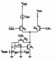
Figure 6.34. Calibration circuit for a single current cell.
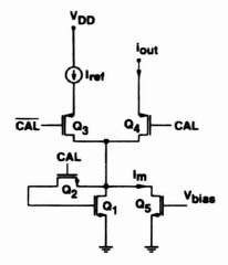
Figure 6.35. Improved calibration circuit for a single current cell.
Two nonideal effects degrade the calibration accuracy of the current cell. These effects, shown in Fig. 6.34, are the channel charge of Q2 which when turned off is partially dumped on the gate of Q1, and the leakage current of the reverse-biased source-to-substrate diode of Q2. Both effects alter the charge that is stored on the gate-to-source capacitor Cgs and hence modify the drain current. It can be shown that decreasing the transconductance (gm) of Q1 can reduce the impact of both nonideal effects on the output (drain) current [19].
The calibration circuit of Fig. 6.34 can be modified by adding a fixed current source in parallel to the current-source transistor Q1. The modified circuit is shown in Fig. 6.35, and the additional current source is represented by transistor Q5, with its gate tied to a fixed bias voltage, Vbias. The added current source has a value of about 90% of the reference current Iref. This reduces the value of Q1's current to about 10% of its original value and decreases its transconductance by a factor of ![]() . Furthermore, since the current of Q1 is lower, its W/L ratio can now be reduced by increasing the length L. In this way it is possible to reduce the transconductance of Q1 further by a factor of 8 to 10 while increasing its Cgs.
. Furthermore, since the current of Q1 is lower, its W/L ratio can now be reduced by increasing the length L. In this way it is possible to reduce the transconductance of Q1 further by a factor of 8 to 10 while increasing its Cgs.
For the calibration technique to be suitable for the DAC of Fig. 6.30, the principle must be extended to an array of current sources. A system that uses the continuous calibration technique for an array of current cells is shown in Fig. 6.36. The principle is characterized by using N + 1 current cells to generate N equal current sources. The current cell number N + 1 is the spare cell. An (N + 1)-bit shift register controls the selection of the cell to be calibrated. One output of the (N + 1)-bit shift register is a logic 1, while the other outputs are all zero. The cell corresponding to the register with the logic level 1 is selected for calibration and is connected to the reference current. Because this cell is now not delivering any current to its output terminal, the output current of the spare cell is switched to this terminal. After completion of a calibration cycle, the contents of the shift register is shifted by one place, and the next cell in the array is selected for calibration. This way, every current cell is sequentially calibrated and inserted back into the array. The switching network is responsible for taking the current source selected out of the array for calibration and replacing it with the spare cell. Since the output of the shift register is connected to its input, after all cells are calibrated sequentially, the first cell is calibrated again. By using one spare cell, no time is lost during the calibration period and there are always N equal current sources available at the output terminals. At this point it is worth mentioning that the purpose of calibration is not to make the value of the current sources precisely equal to Iref but to make the current sources match accurately.
The coarse current array in the DAC of Fig. 6.31 can be replaced with the calibrated current array of Fig. 6.36. The basic block diagram of a 16-bit DAC is shown in Fig. 6.37. The DAC is segmented into 6-bit coarse and 10-bit fine DACs. The coarse current array now consists of 65 calibrated current cells shown in Fig. 6.35. The current outputs of 63 normally functioning cells are connected to 63 two-way current switches, and one cell is connected directly to the 10-bit binary-weighted current divider. The nonfunctioning current cell is connected to the reference current for calibration. In this arrangement since all current cells are calibrated, a unique current cell is dedicated to the fine current divider, unlike the DAC of Fig. 6.33. A simplified version of the calibration circuitry and the current cell is shown in Fig. 6.38. Of the 65 current cells, 63 supply currents to the coarse DAC, one supplies current to the fine current divider, and one cell is being calibrated. For a normally functioning cell, transistors Q2, Q5 and Q7 are off and the current source comprised of transistors Q1 and Q4 supplies the current to the output terminal through the “on” device Q6. For the cell that is being calibrated, devices Q2, Q5, and Q7 are on and Q6 is off. Since the cell is not operational, the spare cell is switched to the corresponding output terminal through device Q7. Notice that terminals An and Bn of all 65 current cells are connected to nodes A and B of the calibration circuitry. For the cell selected, the reference current Iref flows into Q1 through Q5 and the loop between the drain and gate of Q1 is closed by the three transistors Q5, Q8, and Q2. This process charges the gate of Q1 to an appropriate voltage required for maintaining a drain current of Iref. At the end of the calibration period the cell returns to its normal operation and the next cell in the array becomes calibrated. In Fig. 6.38, transistor Q3 has been added for channel charge cancellation. The gates of Q2 and Q3 are connected to the two opposite phases of the control clock. The transistors are identical except that Q3 has half the channel width of Q2. The charge transferred from the control signal to C from Q2 during the falling edge of the clock is canceled by the charge transferred to C by Q3 during the rising edge of the opposite clock.

Figure 6.36. Block diagram of a continuously calibrated array of N current sources.

Figure 6.37. Block diagram of a 16-bit continuously calibrated DAC.
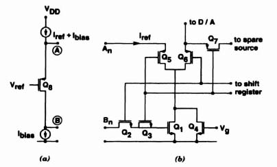
Figure 6.38. (a) Calibration circuitry; (b) current cell.
Sixteen-bit DACs using the continuous calibration technique described in this section have achieved 0.0025% linearity at a power dissipation of 20 mW and a minimum power supply of 3 V [19].
PROBLEMS
6.1. What is the necessary relative accuracy of the resistor ratios in the 8-bit version of the resistive DAC of Fig. 6.4 to achieve 8-bit linearity?
6.2. Prove Eq. (6.4) for the folded resistor-divider DAC of Fig. 6.6.
6.3. Analyze the circuit of Fig. 6.13. Describe ν0(nT) in terms of νin(nT). Assume first infinite, then finite op-amp gain.
6.4. Figure 6.39 shows an offset-compensated voltage amplifier that does not require a high-slew-rate op-amp [9]. Analyze the circuit for both choices (shown in parentheses and without parentheses) of the input-branch clock phases. How much does νout, vary between the two intervals ![]() 1 = “1” and
1 = “1” and ![]() 2 = “1”? Plot the output voltage νout, for both choices.
2 = “1”? Plot the output voltage νout, for both choices.
6.5. Calculate the total capacitance loading node X in an n-bit PCA as shown in Fig. 6.16.
6.6. What is the necessary relative accuracy of the capacitor ratios in the charge-mode D/A converter of Fig. 6.17 to achieve 11-bit linearity?
6.7. Design the two-stage cascaded D/A converter of Fig. 6.19 for 12-bit resolution. Determine the number of the bits in the first and second stages so that the total capacitance is minimized.
6.8. Design a 10-bit hybrid D/A converter using a charge-mode MSB and resistor-mode LSB structure (Fig. 6.20). Determine the relative accuracy of the capacitor and resistor ratios to achieve 10-bit linearity.
6.9. Derive an expression for the number of unit capacitors, resistors, and switches for the N-bit DAC of Fig. 6.21. Assume that N = N1 + N2 where N1 is the number of LSBs assigned to the resistive DAC and N2 is the number of MSBs assigned to the capacitive DAC.
6.10. Design an 8-bit current DAC according to the architecture of Fig. 6.25. Use an equal number of bits for the columns and rows. Design the column and row decoders and the current cell logic.
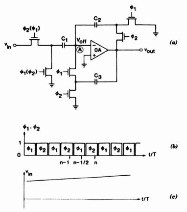
Figure 6.39. Offset-compensated voltage amplifier (for Problem 6.4).
6.11. Repeat Problem 6.10 for the architecture of Fig. 6.26. Design the current reference and the unit currents in such a way that the full-scale output current generates 1 V of peak voltage across a 75-Ω load resistor.
6.12. For the circuit of Fig. 6.29, plot the waveform at node A when Clk goes from low to high and high to low. Assume that the low level is 0 V, the high level VDD (the positive supply voltage), and the p-channel threshold voltage is VDD/5.
6.13. Design the 10-bit version of the segmented DAC of Fig. 6.31. Use 4 bits for the coarse current and 6 bits for the fine current DACs. If the feedback resistor of the current-to-voltage converter is 1 Ω, find the value of the full-scale current if the maximum output voltage is 2 V. What is the value of each coarse current source and the current corresponding to one LSB?
6.14. Figure 6.31 shows a unipolar segmented current DAC where the output voltage varies between 0 V and VFS = RIFS and IFS is the full-scale output current. In a single-supply application, assume that the positive input of the op-amp is connected to VDD/2 (VDD is the positive supply voltage). Modify the circuit of Fig. 6.31 so that the voltage output varies between ![]() (zero input code) and
(zero input code) and ![]() (full-scale input code). Assume that the DAC is 8 bits, VDD = 5 V, and R = 1 Ω. (Hint: Connect a fixed current source to the inverting input of the op-amp.)
(full-scale input code). Assume that the DAC is 8 bits, VDD = 5 V, and R = 1 Ω. (Hint: Connect a fixed current source to the inverting input of the op-amp.)
REFERENCES
1. A. R. Hamadé, IEEE J. Solid-State Circuits, SC-13(6), 785–791 (1978).
2. A. Dingwall and V. Zazzu, IEEE J. Solid-State Circuits, SC-20(6), 1138–1143 (1983).
3. M. J. M. Pelgrom, IEEE J. Solid-State Circuits, SC-25(6), 1347–1352 (1990).
4. A. Abrial et al., IEEE J. Solid-State Circuits. SC-23. 1358–1369 (1988).
5. P. Holloway, ISSCC Dig. Tech. Pap., pp. 66–67, Feb. 1984.
6. Y. A. Haque, R. Gregorian, R. W. Blasco, R. A. Mao, and W. E. Nicholson, IEEE J. Sold-State Circuits. SC-14(6), 961–969 (1979).
7. R. Gregorian, Microelectron. J., 12, 10–13 (1981).
8. R. Gregorian, K. Martin, and G. C. Temes, Proc. IEEE, 71, 941–966 (1983).
9. K. Huang, G. C. Temes, and K. Martin, Proc. Int. Symp. Circuits Syst., pp. 1054–1057, 1984.
10. J. L. McCreary and P. R. Gray, IEEE J. Solid-State Circuits, SC-10(6), 371–379 (1975).
11. R. Gregorian and G. Amir, Proc. Int. Symp. Circuits Syst., pp. 733–736, 1981.
12. K. W. Martin, L. Ozcolak, Y. S. Lee, and G. C. Temes, IEEE J. Solid-State Circuits, SC-22(1), 104–106 (1987).
13. B. Fotouhi and D. A. Hodges, IEEE J. Solid-State Circuits, SC-14(6), 920–926 (1979).
14. T. Miki, Y. Nakamura, M. Nakaya, S. Asai, Y. Akasaka, and Y. Horiba, IEEE J. Solid-State Circuits. SC-21(6), 983–988 (1986).
15. L. Letham, B. K. Ahuja, K. N. Quader, R. J. Mayer, R. E. Larson, and G. R. Canepa, IEEE J. Solid-State Circuits. SC-22(6). 1041–1047 (1987).
16. A. B. Grebene, Bipolar and MOS Analog Integrated Circuit Design, Wiley, New York, 1984.
17. D. A. Johns and K. Martin, Analog Integrated Circuit Design, Wiley, New York, 1997.
18. H. J. Schouwenaers, D. W. J. Greeneveld, and H. A. H. Tremeer, IEEE J. Solid-State Circuits. 23(6), 1290–1297 (1988).
19. C. A. A. Bastiaansen, IEEE J. Solid-State Circuits, 24(6), 1517–1522 (1989).
20. S. R. Norsworthy, R. Schreier, and G. C. Temes, Delta-Sigma Data Converters Theory, Design, and Simulation. IEEE Press, Piscataway, NJ, 1997.