
2 Active CMOS Biochip for Electrochemical DNA Assays
CONTENTS
2.1.1 Electrochemical DNA Sensing
2.1.2 Active CMOS Biochip for Electrochemical DNA Sensing
2.2.1 Affinity-Based DNA Sensors
2.2.3 Fluorescence-Based DNA Microarrays
2.2.3.1 Commercially Available Microarray Systems
2.2.4 Electrochemical DNA Sensors
2.2.4.2 Real-Time DNA Detection
2.2.5 Principles of Electrochemistry
2.2.5.1 Electrode–Electrolyte Interface
2.2.5.2 Electrochemical Reactions at Equilibrium
2.2.5.3 Potentiostat Operation
2.2.6 DNA Immobilization Chemistry
2.2.7 Review of Electrochemical DNA Sensing Techniques
2.2.7.1 Redox-Label-Based Electrochemical DNA Sensors
2.2.8 CMOS Electrochemical DNA Sensors
2.2.8.1 Prior Work on CMOS Electrochemical DNA Sensors
2.3 Design of an Active CMOS Biochip for Label-Based Electrochemical DNA Assays
2.3.1 Label-Based Electrochemical DNA Sensing Method
2.3.2 Active CMOS Biochip System Requirements
2.3.2.3 Working Electrode Area
2.3.2.4 Silicon Area of Sensor Interface Electronics
2.3.3.1 Dual-Slope ADC Architecture and Operation
2.3.3.2 Working Electrode Array
2.3.3.3 Potentiostat Control Amplifiers
2.3.4 Electrochemical Cell Interface Model
2.3.5 Design of ADC Circuit Components
2.3.5.2 Thermal and Flicker Noise
2.3.5.3 Bandwidth and Stability
2.3.5.6 Current Sources and Switches
2.3.5.7 Digital Counter and Control Circuitry
2.3.6 Design of Control Amplifier Circuits
2.3.7 Sensor Detection Limit and Noise Analysis
2.3.7.2 Shot Noise from a Redox Current
2.3.7.3 Thermal Noise from Electrolyte Resistance
2.3.7.4 Amplifier Thermal Noise
2.3.7.5 Amplifier Flicker Noise
2.3.7.7 Target Coverage Detection Limit
2.3.7.8 Effect of Working Electrode Area on Detection Limit
2.3.7.9 Effect of ADC Integration Time on Detection Limit
2.3.8 CMOS Biochip Fabrication and PostProcessing
2.3.8.1 Initial Electrode Fabrication Procedure
2.3.8.2 Improved Electrode Fabrication Procedure
2.4.1 CMOS Chip Packaging and Experimental Setup
2.4.2 Electrical Characterization
2.4.3 Integrated Electrochemical Measurements of a Bulk Redox Species
2.4.3.1 Biochip Preparation and Experimental Procedure
2.4.4 Integrated Electrochemical Measurement of DNA Probe Surface Coverage
2.4.4.1 Biochip Preparation and Experimental Procedure
2.4.5 Label-Based Electrochemical DNA Sensing
2.1 Introduction
The development of methods and technology to perform genome sequencing and genomic assays has enabled significant advances in biomedical research in the past and will have a profound impact on the areas of disease prevention, personalized medicine, and clinical diagnostics in the future [1]. Over the last two decades, enormous effort from the public and private sectors has been spent on “sequencing” the human genome; that is, determining the exact series of the approximately 6 billion nucleotide base pairs contained in the 46 chromosomes found in most human cells. Ever since drafts of the human genome were first published in 2001 by both the publicly funded International Human Genome Sequencing Consortium through the Human Genome Project (HGP) [2] and a team led by J. Craig Venter of the privately owned biotechnology company Celera Genomics [3], the cost of human genome sequencing has declined by many orders of magnitude due to the introduction of increasingly automatable methods and technology. In particular, shotgun sequencing approaches [4] involving dideoxy chain termination techniques and electrophoretic size separation (known as “Sanger sequencing,” after the individual who developed the technique [5]) have been replaced by massively parallel optical [6,7] and electronic [8] sequencing-by-synthesis platforms. These innovations have brought the cost of human genome sequencing down from US$3 billion, in the case of the HGP [9], to well under US$1 million [8]. Further technological developments will undoubtedly occur until one’s own genome can be sequenced for less than US$1000 [10].
In addition to the numerous breakthroughs in DNA sequencing technology, methods and platforms for executing genomic assays have also undergone many advancements. Perhaps the most significant of these was the introduction of DNA microarrays in the mid-1990s. Presently, DNA microarrays are widely used for rapid, quantitative analysis of gene expression on a large scale [11–13]. Microarrays typically use a passive substrate, such as a glass slide, on which single-stranded DNA (ssDNA) “probe” molecules, representing thousands of individual genes, are arranged in a regular pattern. Probes are then allowed to bind to, or “hybridize” with, complementary, fluorophore-labeled ssDNA “target” molecules in an analyte solution. After nonhybridized targets are removed from the array through a washing step, the locations of hybridized targets on the microarray surface are measured with an optical scanner consisting of one or more laser sources for excitation and a photomultiplier tube (PMT) or charge-coupled device (CCD) camera to detect the emitted light. Relative expression levels of bound targets at different array sites can then be quantified from the resulting image.
While DNA microarrays are used extensively by research laboratories worldwide for applications such as transcriptional profiling, genotyping, and epigenetic studies [1], they have found limited use in clinical diagnostics. It is believed that microarray-based tests are superior to traditional DNA-based assays for clinical applications due to their ability to simultaneously measure the relative expression levels of a large number of clinically relevant genes [14]. In addition, microarrays are well suited for use in single-nucleotide polymorphism (SNP) analysis in which the existence of a single-base mismatch on a DNA strand can be used to identify a genetic disorder. However, DNA microarrays have found only limited use in clinical settings because their results often do not meet the stringent accuracy and reproducibility requirements set forth by the clinical and regulatory communities [15]. Despite this, it is expected that the human and biological factors that give rise to poor repeatability can be mitigated through the development and adoption of standardized methods [16].
The high instrumentation cost associated with microarray platforms is another reason why these systems are not widely used in clinical laboratories [14,15]. For example, the entry-level capital cost of optical scanners is typically well above US$100,000, which is too high for many laboratories. However, platform costs can be reduced using alternative detection methods and technologies other than traditional fluorescence-based DNA assays on passive, glass substrates.
In addition to laboratory-based clinical applications, genomic assays based on microarray technology could have future use in point-of-care (POC) genetic diagnostic applications. The ultimate goal would be to create a portable, handheld device for use in a physician’s office, ambulance, or at the hospital bedside that could immediately provide time-critical information about the genetic composition of a patient, bacteria, or virus [17]. Microarrays are well suited to this application because they can screen for numerous illnesses containing many genetic markers and, therefore, could be used for such applications as predicting adverse drug reactions [18] or identifying bacterial or viral infections.
Unfortunately, traditional fluorescence-based DNA microarrays are not well suited for use in POC diagnostics. This is because the bulky and heavy lasers and optical detectors employed in these systems defy portability for POC applications. A platform for genomic assays that does not require light as an intermediary for sensing is, therefore, a valuable alternative.
2.1.1 Electrochemical DNA Sensing
Electrochemical sensing approaches to DNA detection, which have gained interest in recent years but are not yet as well developed as optical techniques [19], have the potential to reduce instrumentation costs and provide portable diagnostic platforms for genomic assays [20]. This is because the need for light as an intermediary for sensing is eliminated and, therefore, no optical equipment is required. Electrochemical DNA sensors instead measure electronic activity that results from hybridization of ssDNA targets with probes immobilized on “working” electrodes (WEs) immersed in an electrolyte. The nature of this electronic activity depends on the sensing methodology used but often involves the introduction of electrochemically active labels on the target DNA. An electronic feedback control system known as a “potentiostat” applies a desired input voltage to the electrochemical cell and measures the resulting current at the WE.
2.1.2 Active CMOS Biochip for Electrochemical DNA Sensing
A complementary metal-oxide-semiconductor (CMOS) platform is well suited to the design of electrochemical DNA sensors for genomic assays because the high level of parallel detection demanded by microarray applications requires active multiplexing. This can only be achieved through integration of the WEs directly onto an active CMOS substrate, known as a “biochip,” containing the sensor electronics. CMOS is also an attractive technology for this application because it can be augmented using standard microfabrication techniques to accommodate the noble-metal electrodes most commonly used in electrochemical sensors.
In addition, the cost of fabricating individual CMOS biochips can become very low by leveraging the tremendous economies of scale associated with the semiconductor manufacturing industry. For example, a complete mask set for a mature CMOS process has a fixed cost on the order of US$50,000 [21]. This is used to fabricate multiple chips on a single silicon wafer that is typically 6–12 inches in diameter. A bare wafer and associated production expenses can cost around US$5000 [22]. This would translate to a typical manufacturing cost per chip of around US$40–US$50, depending on the number of chips manufactured. As a result, affordable diagnostic devices for widespread use in the healthcare industry could be produced relatively cheaply.
CMOS biochips also have much potential for use in POC genetic diagnostic applications because they can be integrated with other technologies to construct compact, self-contained sensing platforms. For example, biochemical sample preparation could be performed in situ using microfluidic channels with integrated pumps and valves [23]; solid-state transducers could be used to detect the presence and concentration of specific genetic sequences in a DNA analyte; and microelectronic integrated circuits could amplify and condition the electronic signals from the transducer, convert this information to a digital format, process it in order to extract relevant biochemical data, and then transmit or display these data externally.
2.1.3 Chapter Overview
This chapter presents an active CMOS biochip for electrochemical DNA sensing to support genomic assays. A CMOS-integrated sensor array is constructed and is designed to perform label-based sensing of DNA surface hybridization in which the redox molecule ferrocene (an electroactive species that undergoes reduction or oxidation depending on the applied potential) is covalently attached to the target DNA. The system consists of a 4 × 4 array of WEs, on which ssDNA probes are immobilized, and full potentiostat electronics, including control-loop amplifiers and a current-input analog-to-digital converter (ADC) at each electrode site. Because only labeled target molecules localized immediately at the electrode surface allow facile electron transfer, no washing step is required as in traditional fluorescence-based DNA microarrays and, therefore, DNA hybridization can be monitored in real time.
2.1.4 Chapter Organization
This chapter is organized as follows. Section 2.2 provides background information on platforms for analyzing DNA and electrochemical-based DNA detection techniques in particular, as well as electrochemistry principles. A review of previous work on electrochemical DNA sensors and CMOS-integrated DNA sensors is also included. Section 2.3 discusses the design and implementation of an active CMOS biochip for label-based, electrochemical DNA assays and Section 2.4 presents experimental results from this biochip [24,25]. Section 2.5 concludes the chapter.
2.2 Background and Review
Affinity-based electrochemical DNA sensors detect charge transfer and interfacial charge fluctuations resulting from surface-based DNA probe–target hybridization. This section provides the necessary background for understanding the operation of electrochemical DNA sensors as well as their construction on active CMOS substrates.
2.2.1 Affinity-Based DNA Sensors
Affinity-based sensors are used to detect the concentration of “target” molecules in a complex analyte based on their specific physicochemical interactions with surface-bound “probe” molecules. This interaction often results in a binding reaction between probe and target to create a “duplex” molecule on the surface. Appropriate transducers are used to convert changes in, for example, light intensity, interfacial capacitance, or mass due to probe–target binding, often to an electronic signal that can be readily observed.
Affinity-based DNA sensors detect changes that occur from hybridization between ssDNA probes and targets and are used widely in genomic assays. Perhaps the most popular platform for constructing large-scale genomic assays that rely on affinity-based molecular interactions is the DNA microarray. Microarrays enable highly multiplexed, parallel detection and have traditionally supported probe immobilization on a passive substrate.
2.2.2 Performance Metrics
Important measures of performance for affinity-based DNA sensors include detection limit, specificity, and dynamic range (DR). The detection limit is usually quoted as the lowest density of target that can be reliably detected on the transducer or microarray surface, or the smallest target concentration that can be detected in solution. A relationship exists between these two values and will be discussed in more detail in Section 2.2.3. Often, a specific signal-to-noise ratio (SNR) is used to define the detection limit (an SNR of 3 is commonly used [26]), where the noise level can be determined from the sensor response to a blank solution.
Specificity refers to the sensor’s ability to respond only to a DNA target in the analyte having a particular sequence and not to other noncomplementary molecules. The DR of the sensor is the ratio of the largest measurable target concentration to the limit of detection [27]. The former variable is often set by saturation of the probe layer with target molecules.
2.2.3 Fluorescence-Based DNA Microarrays
Fluorescence-based DNA microarrays have arguably become the standard technique for quantifying extents of hybridization in multiplexed genomic assays. Applications include gene expression profiling and functional genomics [28,29], drug development [30,31], mutational analysis [32], pharmacogenomics [33], and evolutionary studies [34]. Figure 2.1 displays the setup of a typical microarray experiment in which up to a million distinct groups of ssDNA probe molecules are immobilized in an array format on an electronically passive substrate such as glass, plastic, or silicon (Si). The 106–1010 ssDNA molecules at each site all contain the same known nucleotide sequence, but the sequence is intentionally varied from site to site. In “oligonucleotide” microarrays (made popular by Affymetrix GeneChip technology), the number of bases comprising each probe molecule is small (between 15 and 70) and represents subsequences of a gene [35]. Conversely, “complementary DNA” (cDNA) arrays can contain entire genes at each site and, therefore, use probes having lengths in the hundreds to thousands [36]. Probes can be constructed externally using solid-phase chemical synthesis and then immobilized on the microarray through mechanical contact “spotting” or noncontact ink-jet printing to create 10–100 μm reaction zones [28]. In this case, silanization of glass [37] or the treatment of Si substrates with an organic film [38] supports covalent probe attachment to the surface. Alternatively, probes can be constructed in situ using photolithographic techniques [39].
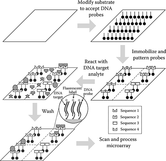
FIGURE 2.1 A typical fluorescence-based DNA microarray for a genomic assay. (Adapted from Patounakis, G., Active CMOS substrates for biomolecular sensing through time-resolved fluorescence detection, PhD. Dissertation, Columbia University, New York, NY, 2005.)
Single-stranded DNA target molecules, having an unknown sequence of bases, are conjugated with chemical labels that, upon absorbing photons at one wavelength, emit photons at a longer wavelength due to energy loss from vibrational or conformational mechanisms. This wavelength translation is expressed as the “Stokes shift.” Fluorescent dyes, such as Cy3, Cy5, and fluorescein, are commonly used as labels and usually emit light with wavelengths in the 500–700 nm range.
When the target analyte is introduced to the microarray, probes and targets hybridize to an extent defined by the magnitude of the equilibrium association constant Ka for the binding reaction. The value of Ka is valid only for a particular temperature, hybridization-buffer ionic strength, and probe and target sequence [41]. Probes and targets that are fully complementary exhibit kinetics that give rise to a higher Ka compared to those having fewer complementary bases. Hybridization of surface-bound probe P to target T in solution to form a duplex molecule PT on the surface can be expressed as a single-step, reversible reaction:
2.1 |
Assuming the above reaction reaches equilibrium, Ka is given by
2.2 |
where:
kf and kr | are the forward and reverse rate constants of the reaction, respectively |
SP | is the surface coverage (density) of hybridized and nonhybridized probe molecules |
ST | is the surface coverage of a particular hybridized target |
CT | is the solution concentration of the target |
A | is the microarray spot area |
V | is the volume of hybridization buffer |
NA | is Avogadro’s number |
If it is assumed that the solution target concentration changes very little as a result of probe–target surface binding, that is CT ≫ ST(A/NAV), then Equation 2.2 can be simplified to
2.3 |
where x is known as the “fractional occupancy” and is given by x = ST/SP [42]. Rearranging the above equation slightly gives:
2.4 |
which shows that the absolute target concentration in solution can be determined if the fractional occupancy and equilibrium constant are known. However, due to the difficulty in characterizing and measuring these parameters accurately in complex, multitarget analyte, microarray analyses are usually limited to relative, as opposed to absolute, target concentration measurements [43].
The array is usually exposed to the analyte for many hours so that the hybridization process approaches equilibrium. Afterward, the array must be washed so that unbound targets and targets that have nonspecifically attached (adsorbed) to the microarray surface are completely eliminated from the substrate. This helps to reduce the background “noise” level. One implication of this is that hybridization cannot be monitored in real time using conventional microarrays, that is, throughout the entire binding process. This is because the analyte would have to be removed from the microarray with a washing step before equilibrium is reached in order to obtain a meaningful signal.
2.2.3.1 Commercially Available Microarray Systems
The size and weight of commercial fluorescence-based microarray scanners and imagers on the market today make them impractical for use in POC diagnostic applications. Commercial microarray systems are almost always manufactured as monolithic, laboratory-scale instruments in which the light source, optics, and detectors are all self-contained [44,45]. The Affymetrix GeneChip Scanner 3000 7G, for example, has dimensions (W × H × D) of 33 × 46 × 56 cm and weighs approximately 32 kg [44]. Although these instruments are bulky and heavy, their detection limit is very low at around 0.05–0.1 fluors μm–2. This corresponds to approximately 106 hybridized targets/cm2, assuming each DNA target has been conjugated with 10 fluorescent labels on average [36].
2.2.4 Electrochemical DNA Sensors
As discussed in the introduction, electrochemical DNA sensors translate affinity-based chemical reactions involving nucleic acids directly to an electronic signal, completely eliminating the need for light. This not only results in platform size reduction, but also supports real-time monitoring of DNA hybridization, which is difficult, if not impossible, using conventional fluorescence-based microarrays. Furthermore, electrochemical techniques have the potential to eliminate the need for chemical labels in DNA assays.
2.2.4.1 Sensing Methodology
Electrochemical DNA sensing is carried out in this work using a method analogous to fluorescence-based DNA sensing. As shown in Figure 2.2, ssDNA probes are first immobilized on an electrode made from a noble metal, such as gold (Au), immersed in an electrolyte (Figure 2.2a). Next, DNA targets that have been labeled with an electroactive chemical species are introduced to the electrolyte and allowed to interact with the probes (Figure 2.2b). These labels are designed to transfer an electron to the electrode when a potential is applied. An electrochemical cell is then established by applying a potential between the Au electrode and a second electrode using the voltage source V (Figure 2.2c). When this occurs, only those labels attached to surface-hybridized targets are able to transfer electrons to the electrode. A quantitative measure of the amount of surface hybridization is obtained by monitoring the level of dc current I using the ammeter A.

FIGURE 2.2 The electrochemical DNA sensing technique used in this work. (a) DNA probes are immobilized on an Au electrode and immersed in an electrolyte. (b) DNA targets conjugated with electroactive labels are introduced. (c) An applied potential causes the labels on hybridized DNA targets to transfer charge to the electrode. The current measured is proportional to the amount of surface hybridization.
2.2.4.2 Real-Time DNA Detection
Many electrochemical DNA sensors allow for real-time detection of the hybridization process because only chemical changes resulting from an affinity-based reaction localized near the electrode surface give a positive signal. As a result, a washing step to remove unbound and nonspecifically bound targets is unnecessary.
Observation of the entire hybridization process in real time has several advantages. First, the point at which equilibrium has been reached can be determined unambiguously so that assay reproducibility and sensitivity can be improved [46]. Second, kinetic studies of DNA binding can be carried out in order to provide insight into the physical properties governing affinity-based reactions [47]. Third, the additional data provided by real-time sensing allow temporal averaging of the measured signal. This could improve the SNR by reducing the effect of independent noise sources. Some of these include nonideal instrumentation and interfering biochemical processes like cross-hybridization, which become more noticeable in assays exhibiting low expression levels [48,49].
2.2.5 Principles of Electrochemistry
Electrochemistry is a branch of chemistry that deals with the processes and factors that influence the charge distribution around, and transport across, an electrode–electrolyte interface. Electrochemical DNA sensing involves relating this charge to the extent of DNA hybridization at an electrode surface. In this section, basic principles of electroanalytical chemistry and electrochemical instrumentation relevant to the design and validation of an active CMOS biochip for electrochemical DNA assays are presented.
2.2.5.1 Electrode–Electrolyte Interface
When an electrode is immersed in an electrolyte containing water molecules and solvated and unsolvated anions and cations, “layers” of charge form at the interface in order to maintain electrical neutrality, as shown in Figure 2.3. These layers can be modeled as two series capacitors having an overall capacitance per unit area of

FIGURE 2.3 The distribution of charges at an electrode–electrolyte interface.
The first capacitor can be modeled as a parallel-plate capacitor having a value that is independent of the electrolyte concentration. This “Helmholtz” layer is composed of solvated positive ions physically separated from the negatively charged electrode surface by a monolayer of water molecules and ions attached to the surface. The capacitance per unit area
2.5 |
where:
Є | is the dielectric constant of the medium |
Є0 | is the permittivity of free space |
d | is the distance between the two layers of charge |
The second capacitor (proposed by Gouy and Chapman) arises from the Boltzmann distribution of ions in a “diffuse layer” beyond the Helmholtz layer. Unlike CH, the capacitance per unit area of the diffuse layer,
The overall capacitance per unit area of the interfacial region
2.6 |
which arises from the Gouy–Chapman–Stern model of the interface. For simplicity, this structure is often referred to entirely as the “double-layer capacitance.”
2.2.5.2 Electrochemical Reactions at Equilibrium
Assume the following reaction occurs at an electrode immersed in an electrolyte containing a bulk reduction–oxidation (redox) species:
2.7 |
where:
O and R | are the oxidized and reduced form of the redox species, respectively |
n | is the number of electrons oxidized or reduced per molecule |
Then, the potential E developed across the double layer of the electrode–electrolyte interface (relative to a specific reference electrode) is given by the Nernst equation:
2.8 |
where:
E0 | is the standard potential at which the reaction in Equation 2.7 proceeds |
R | is the molar gas constant |
F | is the Faraday constant |
CO and CR | are the concentrations of the oxidized and reduced forms of the redox species, respectively |
The above equation holds only under equilibrium conditions, where no current flows across the interface.
2.2.5.3 Potentiostat Operation
A potentiostat can be used to investigate the interface under nonequilibrium conditions. A potentiostat is a feedback control system used to apply a desired potential to an electrode–electrolyte interface and to measure simultaneously the movement of charge through the interface. A standard potentiostat used in a typical electrochemical cell, shown conceptually in Figure 2.4a, consists of three electrodes immersed in an electrolyte: a WE at which the reaction of interest occurs and where DNA probes would be immobilized when performing DNA sensing, a “reference” electrode (RE) to hold the electrolyte at a known potential, and a “counter” electrode (CE) that behaves like an anode or cathode depending on the direction of charge flow.
The voltage source V between WE and CE is adjusted to establish a desired cell input voltage Vin between the WE and RE. Direct current I can flow through the external circuit (as measured by the ammeter A) as redox species in the electrolyte, for example, donate electrons to the WE and accept electrons from the CE. In addition, a displacement (charging) current can flow as ions segregate to the WE and CE to form space-charge regions. The high-impedance voltmeter (VM) attached to the RE ensures that very low current flows through this interface, maintaining it at equilibrium.
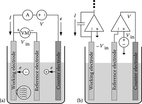
FIGURE 2.4 Description of potentiostat operation. (a) Conceptual diagram. (b) Implementation using standard electronic components.
The basic potentiostat circuitry in Figure 2.4a can be implemented using standard electronic components, as shown in Figure 2.4b. The operational amplifier (op amp) on the right establishes the control loop, while the integrator on the left converts the current flowing through the WE to a voltage for digitization and readout. Only a very small current flows through the RE due to the high input impedance of the control amplifier.
2.2.5.4 Electrode Materials
A wide range of materials are generally used to construct the WEs, including metals, oxides, and semiconductors. These are normally selected to provide a highly polarizable (capacitive) interface when immersed in an electrolyte. Gold is the WE material used in the detection system implemented in this work because it is relatively electrochemically inactive (i.e., it will not react with the electrolyte under normal operating potentials and interfere with the chemical processes being studied) and enables straightforward DNA attachment chemistry.
The RE usually exhibits a nonpolarizable interface that is in chemical equilibrium with the electrolyte, thus providing a stable potential to which the WE potential is referenced. One of the most common RE materials is a silver (Ag) wire coated with a layer of silver chloride (AgCl) formed by anodization in a chlorine-containing solution or through exposure to, for example, common household bleach. When the Ag/AgCl wire is placed in a glass reservoir having a salt bridge containing a 3 M sodium chloride (NaCl) filling solution, the following redox reaction provides a stable electrochemical potential:
2.9 |
Platinum (Pt) is commonly used for the CE because of its inertness. Other noble metals, like Au, can also be used.
2.2.5.5 Cyclic Voltammetry
The active CMOS biochip described in Section 2.3 applies cyclic voltammetry (CV), a large-signal electrochemical measurement technique. CV is one of the most popular techniques for studying the behavior of electrochemical systems because it can rapidly provide considerable information on the thermodynamics of redox processes, the kinetics of multistep electron transfer reactions, and surface-based chemical processes [50]. In this work, CV is used to measure bulk redox species as well as quantify the extent of DNA hybridization at an electrode surface using redox labels.
Figure 2.5 shows how CV is typically executed. In CV, voltage Vin (always expressed relative to a standard RE potential, denoted here as Vre) is set to the initial voltage Vi, ramped up to the vertex potential Vν at the scan rate ν, and then ramped down at the same rate until the final voltage Vf (usually equal to Vi) is reached, while the current flowing through the WE, Iwe, is measured simultaneously. When detecting redox species present in the bulk solution, Iwe as a function of time appears as shown in Figure 2.5. However, Iwe is normally viewed as a function of Vin so that the potentials at which reduction, Ep,c, and oxidation, Ep,a, occur (indicated by the forward and reverse current peaks, respectively) may be easily discerned. These potentials, as well as the value of Iwe at each peak, indicate the degree of reversibility of an electrochemical reaction as well as the amount of chemical product generated or reactant consumed [51]. The peak current ip for a reversible redox couple (at 25°C) such as that in Equation 2.7, is given by the Randles–Sevcik equation [50]:

FIGURE 2.5 Cyclic voltammetry of an electrochemical cell containing a bulk redox species.
2.10 |
where
The separation ΔEp between Ep,c and Ep, a for a reversible couple is given by
2.11 |
A surface-bound (adsorbed) redox species is not affected by mass-transfer limitations and, therefore, exhibits a current response during CV that differs from that of a bulk redox species. The current response from redox-labeled ssDNA targets follows the same behavior as an adsorbed species because these molecules effectively become “attached” to the electrode surface upon hybridization. Assuming only the adsorbed species O in Equation 2.7 is electroactive, while dissolved O out in the electrolyte is inactive, the redox current iad is given by [52]
2.12 |
where:
SO | is the surface density of adsorbed O |
bO and bR | are the adsorption coefficients of O and R, respectively |

FIGURE 2.6 Cyclic voltammetry measurement of an electrochemical cell containing an adsorbed redox species.
Figure 2.6 displays the characteristic shape of this response. Assuming bO = bR, the peak current iad,p can be calculated using
2.13 |
2.2.6 DNA Immobilization Chemistry
Thiol-metal chemisorption is used in this work to immobilize ssDNA probes on the surface of a WE. Oligonucleotide probes are modified with a thiol (–SH) group at one end. The strong affinity of this group for a noble metal surface, such as Au, enables the formation of bonds between the sulfur (S) and Au atoms as follows [53,54]:
2.14 |
where R is a linker such as (CH2)6 [55]. Typical surface coverage of probe molecules using this technique is between 1011 and 1013 molecules cm–2. This depends largely on the immobilization buffer concentration and exposure time.

FIGURE 2.7 Backfilling the electrode surface with an alkanethiol self-assembled monolayer lifts the DNA probes off the surface, enhancing hybridization efficiency.
“Backfilling” the electrode surface with an alkanethiol self-assembled monolayer (SAM) such as mercaptohexanol (MCH) after immobilization of thiolated ssDNA probes is necessary to reduce nonspecific adsorption of probe on the surface. This is because the thiol group on the MCH has a higher affinity for Au than the less strongly adsorbed DNA bases have. This leaves the DNA attached to the Au by the end-point thiol group only, effectively lifting the probe off the surface [56], as displayed in Figure 2.7. In addition, the net negative dipole of the alcohol end group repels the DNA backbone, helping to project the probe strand out into solution [57]. This helps to increase hybridization efficiency because the probes have more configurational freedom to form a duplex molecule by coiling around the analyte DNA targets.
2.2.7 Review of Electrochemical DNA Sensing Techniques
Affinity-based electrochemical DNA sensors can be divided into two broad categories: label-based and label-free. In the former, an electroactive chemical label or enzyme attached to the target DNA or a secondary DNA support provides the positive electrochemical signal. Alternatively, this signal can be derived from redox indicator molecules, which associate differently with DNA duplexes than with ssDNA molecules.* Conversely, label-free DNA sensors require no supporting redox species, enzymes, or indicator molecules to provide the electrochemical signal. Instead they rely on, for example, oxidation of individual DNA bases or changes in interfacial capacitance or surface charge due to DNA hybridization. Electrochemical DNA sensors used in biological applications are often referred to as “biosensors” because the reactions of interest occur directly on the transducer surface [54]. Label-based sensing with electroactive redox labels is now discussed in more detail as the active CMOS biochip discussed in this chapter makes use of this approach.
2.2.7.1 Redox-Label-Based Electrochemical DNA Sensors
Chemical modification of DNA targets with an electroactive redox label, enzyme [58,59], or metal nanoparticle [60,61] is used to enhance the detection limit of DNA sensors. Ferrocene is a commonly used redox label because it is easily functionalized and is electrochemically reversible. In addition, it possesses a known redox potential that does not coincide with that of the DNA bases [62]. Ferrocene tags have been used to label phosphoric-, amino-, and thiol-modified ssDNA targets [63]. When these are hybridized to complementary DNA probes on a graphite electrode, the peak anodic current from a differential pulse voltammetry measurement is proportional to the concentration of surface-hybridized probes [64].
Ferrocene is the redox label used in GenMark Diagnostics’ eSensor DNA chip [65] (which was originally developed by Motorola’s Clinical Micro Sensors Division). In this “sandwich” assay, the ferrocene label is covalently attached to the ribose backbone of a short oligonucleotide signaling probe that selectively binds to a DNA duplex on an Au electrode after hybridization has occurred. The peak Faradaic current measured using ac voltammetry is directly proportional to the number of ferrocene moieties present, which is also proportional to the number of surface-hybridized DNA targets. This system has been used for various clinical applications, including the detection of hemochromatosis [66], human papillomavirus [67], and cystic fibrosis [68].
2.2.8 CMOS Electrochemical DNA Sensors
There are currently only a few commercially available electrochemical sensor platforms for clinical genomic assays and none for POC genetic diagnostic applications. This is partly due to the numerous technical challenges encountered when designing a compact device that must incorporate a highly multiplexed transducer interfaced with electronic readout circuitry. Specifically, electrochemical readout normally requires a wired mechanical connection between the electrode and potentiostat electronics. Therefore, the fabrication and interfacing of arrays of microelectrodes on a passive substrate to permit detection of hundreds to thousands of individual sequences for gene-expression and mutation diagnostics presents a significant engineering challenge [19].
Integration of electrode transducer arrays, potentiostat electronics, and digital readout together on an active CMOS substrate enables the construction of portable, highly multiplexed electrochemical DNA sensing platforms for clinical and POC genetic diagnostic applications. This system therefore requires immobilizing DNA probes at electrode sites on the surface of the CMOS chip and carrying out all DNA hybridization reactions there as well. In addition to increased multiplexing and enhanced portability, integrated electronic instrumentation reduces susceptibility to electromagnetic interference that can result from transmitting nonamplified analog signals off chip.
2.2.8.1 Prior Work on CMOS Electrochemical DNA Sensors
Previous work on CMOS-integrated affinity-based electrochemical DNA sensors has involved both label-based and label-free detection. Much of this prior work has focussed on specific modalities of potentiostatic sensing, such as redox cycling and capacitance-to-frequency conversion, to simplify the electronics. In addition, field-effect DNA sensing using special ion-sensitive MOS transistors has been reported. These are all described in more detail below.
2.2.8.1.1 Field-Effect Transistor–Based DNA Sensing
Integrated MOSFETs have been used to perform direct label-based and label-free electronic detection of DNA sequences. DNA probes are usually immobilized on the surface of the oxide above the transistor channel [69,70], directly on an aluminum (Al) electrode above the polysilicon gate of the transistor [71], or on a postprocessed Au thin-film electrode covering the Al [72]. Detection has been performed by monitoring changes in the channel current that result from fluctuations in the electrode surface charge due to DNA hybridization [72]. Alternatively, the transistor current–voltage characteristics can be measured before and after hybridization to determine the resulting threshold-voltage shift [71]. In addition, Ion Torrent (Guilford, CT) has developed and marketed massively parallel CMOS-integrated ion-sensitive FET (ISFET) arrays for detecting hydrogen ion release resulting from nucleotide base incorporation through template-directed DNA polymerase synthesis [8].
2.2.8.1.2 CombiMatrix CMOS Electrochemical DNA Microarray
An electrochemical DNA microarray platform once developed and marketed by CombiMatrix (Mukilteo, WA) consisted of a CMOS microarray chip having more than 12,000 individually addressable, 44 μm diameter, Pt microelectrode sites, and an external (off-chip) reader [73]. The reader contained electronic actuation and measurement circuitry and interfaced with the CMOS microarray chip.
Detection involved a sandwich assay in which biotinylated target DNA first hybridized with immobilized probes. After this, horseradish peroxidase (HRP) was attached to the bound targets using biotin–streptavidin chemistry, which helped catalyze the oxidation of the added species tetramethylbenzidine (TMB). Current generated from the reduction of oxidized TMB from an applied potential was then used to quantify the target concentration. This system was used in influenza A geno-typing applications and reportedly provided nearly identical results in certain gene expression studies using standard fluorescence-based DNA microarrays [73].
2.2.8.1.3 Infineon CMOS Electrochemical DNA Microarrays
Schienle et al. at Infineon Technologies (Neubiberg, Germany) have developed CMOS microarrays for detecting DNA oligonucleotides using a redox cycling method in which electronic measurement circuitry is integrated on the same chip as the electrodes. DNA probes are immobilized on an array of 128 interdigitated Au generator and collector electrodes in a 0.5 μm CMOS process [74]. Targets are labeled with the enzyme alkaline phosphatase in the presence of an added paraaminophenylphosphate chemical substrate that is cleaved following hybridization. Upon cleavage, the electrochemically active compound para-aminophenol (p-AP) is produced, which can then be oxidized and reduced by applying a potential of +200 mV and –200 mV to the generator and collector electrodes, respectively. The current produced is measured using an in-pixel current-to-frequency ADC and can be related to the DNA surface coverage. Potentiostat electronics including a control amplifier and CE and REs are also integrated. This system offers highly multiplexed DNA detection with relatively simple and compact readout circuitry, but requires a complex full-back-end CMOS process to create an array of Au electrodes on the surface [75]. Furthermore, real-time monitoring of DNA hybridization is not possible with this platform.
2.2.8.1.4 Toshiba CMOS Electrochemical DNA Sensor Array
Gemma et al. of Toshiba reported a CMOS DNA chip having 40 on-chip Au WEs ranging in diameter from 2 to 200 μm [76]. The redox “groove binder” Hoechst 33258 is introduced to the assay following DNA hybridization. The peak current level produced from Hoechst oxidation during linear-sweep voltammetry is used to provide the hybridization signal. The system includes an integrated potentiostat as well as an individual mirror-based current amplifier and continuous-time current-to-voltage converter connected to each electrode. DNA target concentrations down to approximately 1 nM are observed using this platform. Despite the high overall performance of this system, real-time sensing is not possible.
2.2.8.1.5 Capacitance-Based and Other Label-Free CMOS Electrochemical DNA Sensors
Previous work on label-free CMOS DNA sensors has involved detecting capacitance changes and electropolymer redox reactions in response to DNA surface hybridization. Hassibi and Lee reported on a 10 × 5 CMOS electrochemical array designed to sense biomolecular reactions occurring at on-chip 60 × 60 μm2 Al WEs [77,78]. Each electrode is connected to a pseudodifferential amplifier network that can be programmed to implement either a transimpedance amplifier, field-effect (ISFET) sensor, or current integrator. The amplifiers also incorporate switched biasing to reduce flicker noise.
Stagni et al. have reported a label-free CMOS DNA sensor for detecting changes in capacitance due to DNA hybridization occurring on an integrated 8 × 16 electrode array [79]. The measurement technique involves periodically switching the current flowing through two interdigitated Au electrodes (with a similar structure and deposition procedure as described in [74]) functionalized with DNA probes, and detecting the transient charging and discharging voltage waveform produced between the electrodes. Since the time constant of this transient signal is proportional to the electrode interfacial capacitance, the frequency of this waveform over many switching cycles can be related to capacitance changes caused by DNA hybridization. Detectable capacitance changes of more than 1 nF due to specific DNA hybridization at the on-chip electrodes have been reported.
A CMOS electrochemical DNA detection system from Heer et al. was used to detect DNA hybridization occurring at a 24 × 24 array of integrated polypyrrole-coated platinum electrodes having diameters between 10 and 40 μm [80]. Changes in the total charge transferred by the surface layer are measured before and after hybridization using CV. These fluctuations are caused by changes in the interaction between chloride ions in the electrolyte and the polymer as negatively charged DNA is brought to the surface. The sensor chip is fabricated in a 0.6 μm process and contains 24 acquisition channels, each consisting of a delta-sigma ADC that uses the intrinsic capacitance of the electrode–electrolyte interface to integrate the charge transferred from the electrode during CV.
2.2.8.1.6 CMOS Microarray for DNA Polymerization Detection
Anderson et al. developed a label-free, 5 × 5, CMOS-integrated microarray to detect DNA using a sequencing-by-synthesis approach [81]. The individual deoxynucleo-tide triphosphates (dNTPs) are added to the analyte one after another and can bind to the individual bases in ssDNA targets immobilized at planar electrodes on the SiO2 surface. The enzyme DNA polymerase must be present in solution for base incorporation to occur. When a single nucleotide is incorporated, integrators at each array site measure the induced charge arising from the diffusion of protons away from the electrode.
2.3 Design of an Active CMOS Biochip for Label-Based Electrochemical DNA Assays
This section describes the development of an active CMOS biochip for multiplexed, real-time, electrochemical DNA assays using a label-based sensing approach. Unlike previously reported CMOS electrochemical sensors, the proposed system uses CV and redox-labeled DNA targets to provide a quantitative measure of DNA hybridization in real time. The proposed biochip contains integrated potentiostat control amplifiers to establish an on-chip electrochemical cell, and an array of thin-film, Au WEs on which DNA probes are immobilized. Each WE is connected to an integrated dual-slope ADC to sense the current produced by surface redox reactions resulting from electron transfer during CV measurements. Postprocessing is necessary to construct a biologically compatible surface-electrode array on the fabricated standard-CMOS biochip that can withstand operation in a harsh electrochemical environment.
2.3.1 Label-Based Electrochemical DNA Sensing Method
Quantitative, real-time electrochemical measurement of surface hybridization on the active CMOS biochip is carried out using DNA targets covalently modified with N-(2-ferrocene-ethyl) maleimide (simply referred to as “ferrocene”) redox labels. Ferrocene (Fc) undergoes the redox reaction
2.15 |
over a potential range between 0 and +0.35 V (vs. a standard Ag/AgCl/3 M NaCl RE). In this work, each DNA target is conjugated with a single Fc redox label. A quantitative measure of the extent of surface hybridization is obtained by integrating the amount of charge transferred during Fc oxidation and then relating this value to a surface target coverage.
The classic electrochemical measurement technique, CV, discussed in Section 2.2, is used to drive the redox reaction associated with the Fc label. Figure 2.8 shows the usual arrangement of the three-electrode potentiostatic cell, the input voltage waveform, and the expected output current from the Fc redox reaction. Using CV, Vin applied to the control amplifier input starts at 0 V, is ramped up to +0.35 V at the scan rate V, and is then ramped back down to zero at the same rate. Fc labels attached to hybridized DNA targets are oxidized during the forward scan and reduced in the reverse scan. As discussed in Section 2.2.5.5, the overall shape of iwe in Figure 2.8 is attributed to the fact that Fc is a surface (rather than a bulk) redox species. The non-Faradaic baseline (charging) current ich is due to the WE capacitance
2.16 |
The density of hybridized probe–target pairs on the WE surface can be determined by integrating the area enclosed by the Fc redox (Faradaic) current after subtraction of background charging contributions, and then dividing the result (in coulombs) by the magnitude of the electronic charge and by the WE area. The charge passed from the forward or reverse scans, or the average of the two, may be used in this calculation.

FIGURE 2.8 Electrochemical quantitation of Fc-labeled DNA targets hybridized to probes on the surface of a WE using CV. A potentiostat applies vin to the WE interface and the redox current iwe is measured using an integrator and an ADC.
2.3.2 Active CMOS Biochip System Requirements
The range of sensor input current, sensor bandwidth, and chip area constraints are the most important factors in selecting a suitable architecture for the CMOS biochip. Each of these is described in more detail below. The sensor detection limit, which depends on the noise contributed from the electronics and the electrochemical and biological processes occurring at the chip surface, is also an important factor and will be analyzed for the chosen architecture in Section 2.3.7.
2.3.2.1 Input Current Range
Measurement of the small currents produced by surface redox reactions in an electrochemical cell requires amplification prior to readout. Determining the range of input currents produced by Faradaic and non-Faradaic processes is necessary when designing the amplification circuitry. The maximum total current iwe,max produced during CV measurements is given by
2.17 |
where iad,p, defined previously in Equation 2.13, is the peak current produced by an adsorbed redox species and ST is the surface target coverage.
The graph in Figure 2.9 shows iwe,max as a function of coverage of Fc-labeled targets on a 100 × 100 μm2 WE for a Cwe of 10 μF cm–2 and CV scan rates of 0.01 and 60 V s–1. These values are in the expected range for the given parameters. The value of iwe,max ranges from 10 pA up to 1 μA, depending on the scan rate and surface target coverage. For coverage below approximately 1011 cm–2, the total current is dominated by the concentration-independent charging current. Hybridized target coverage above about 2 × 1013 cm–2 is difficult to achieve in practice due to the significant electrostatic repulsion caused by the correspondingly high probe coverage [82].
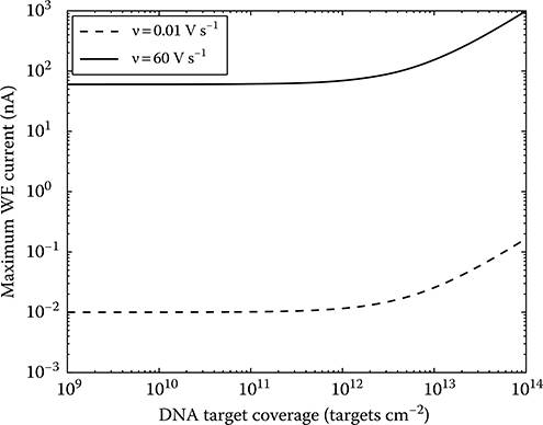
FIGURE 2.9 Expected maximum input current as a function of surface density of hybridized DNA targets for two CV scan rates.
2.3.2.2 Bandwidth
The required bandwidth of the sensor interface circuitry and ADC sampling rate depends on the bandwidth of the input WE current signal. CV measurements are usually performed at relatively low frequencies. Applying a periodic triangular voltage signal to the control amplifier at a scan rate of 60 V s–1 over a 0.35 V range corresponds to an effective frequency of approximately 85 Hz. Assuming the sensor electronics must have a bandwidth 10 times the input voltage frequency to accurately reconstruct the measured current, a 1 kHz sensor input bandwidth is sufficient. Additionally, a 10 kHz ADC would provide over 100 samples of the current waveform produced by the CV measurement above.
2.3.2.3 Working Electrode Area
The density of WEs on the CMOS surface can be increased by reducing the WE area. However, shrinking the WEs also reduces the signal current derived from the redox labels. As a result, the demands on the noise performance of the sensor electronics might become too great to achieve a tolerable SNR. This is discussed in more detail in Section 2.3.7.
2.3.2.4 Silicon Area of Sensor Interface Electronics
Dedicating an individual current sensor and ADC to each WE in the array enables real-time observation of DNA hybridization occurring at all WEs simultaneously. However, allocating one measurement device per WE could consume a great deal of silicon area and would ultimately limit the maximum density of on-chip WEs. Therefore, a compact interface is desirable.
2.3.3 System Architecture
The overall architecture of the active CMOS biochip is displayed in Figure 2.10. It is composed of a 4 × 4 array of sensor sites where each site contains a square Au WE and a current-input dual-slope (integrating) ADC to measure bidirectional redox and charging currents. Integration-based sensor interfaces are often used in low-current potentiostat applications [83–87]. Potentiostat control amplifiers, connected to integrated CEs and an external RE, establish the on-chip electrochemical cell. Each of these components is discussed in more detail below.

FIGURE 2.10 Architecture of the active CMOS biochip for label-based electrochemical DNA sensing.
2.3.3.1 Dual-Slope ADC Architecture and Operation
The dual-slope ADC, shown in Figure 2.11, is composed of an integration op amp with the feedback capacitor Cf, two current sources having opposite polarity, a track-and-latch comparator, switches to activate the various components according to the dual-slope algorithm, and digital control circuitry. The dual-slope ADC is well-suited to low-current CV measurements and can provide moderate resolution (9–12 bits) at kilohertz sampling rates. In addition, the current input range can be easily programmed by digitally varying the duration of the temporal integration and discharge intervals. Furthermore, the dual-slope ADC provides an accurate measure of the input current over a wide range that does not depend on the absolute value of Cf. This is advantageous because the absolute value of CMOS-integrated passive components can vary by more than ± 20% due to inaccuracies inherent in CMOS manufacturing [88].
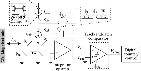
FIGURE 2.11 Architecture of the dual-slope ADC.
Figure 2.12 displays the three steps of the dual-slope algorithm. In the first step in Figure 2.12a, the capacitor is reset when the switch controlled by φ1 is closed and the integrator output Vint is set to the virtual ground voltage Vcm. Next, current flowing through the WE Iin is integrated onto Cf for a fixed time interval t1 by asserting the signal φ2, as shown in Figure 2.12b. The value of Vint rises when Iin flows in the direction shown. The following expression can be written for the integration capacitor:
2.18 |
The comparator connected to the clock signal φclk indicates the direction (sign) of Iin by comparing Vcm to Vint. In the final step, digital control circuitry detects the comparator’s binary output and selects the current source having the opposite polarity as Iin. As shown in Figure 2.12c, the known current Iin+ is integrated onto Cf when the switch connected to φ3a is closed. The time t2 required to change the sign of the comparator output is determined when Vint crosses Vcm. A second expression can be written for the integration capacitor:
2.19 |
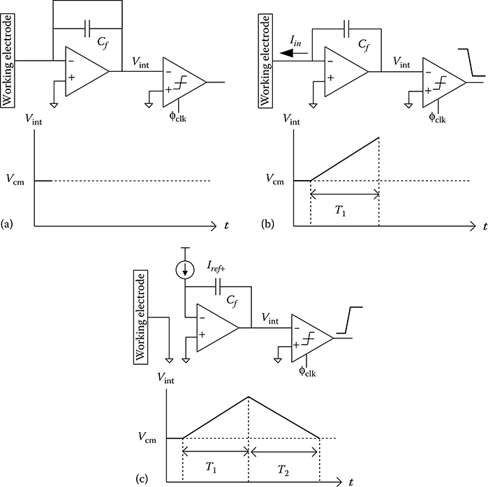
FIGURE 2.12 The dual-slope ADC algorithm. (a) Resetting of the integration capacitor during the first phase. (b) First integration period during which the WE current is integrated onto Cf. (c) Second integration period in which the appropriate current source is activated.
Equating equations 2.18 and 2.19, and solving for Iin gives:
2.20 |
Therefore, an accurate measure of Iin is obtained that is independent of the absolute value of Cf. Time t1 is set and t2 measured using a digital counter operating at the frequency of φclk. This rate is much higher than the overall ADC sample rate. The number of bits in the counter sets the nominal resolution of the ADC and effectively quantizes t2. The minimum sampling period is the sum of the reset time, t1, and the maximum value of t2 allowed, t2,max. A short time interval td is also necessary to allow for the selection of the appropriate current source before the second integration period. The ADC is also designed such that the WE is always connected to Vcm, whether it be directly through a switch or to the virtual ground of the integration amplifier. This helps to maintain the desired potential between the WE and RE that is necessary for accurate electrochemical measurements.
The dual-slope ADC also has an “autozeroing” mechanism to reduce the effect of amplifier and comparator offsets on the digital output. Offset removal mitigates the effect of flicker noise on the output and helps to reduce mismatch (i.e., “fixed-pattern” noise) among sensor sites. When the autozeroing signal φaz is asserted in Figure 2.11, only current due to amplifier offset is integrated onto Cf. The digital value representing this current, which is also affected by comparator input offset, can then be subtracted from the digitized WE current. Autozeroing can be performed before each ADC sampling cycle to reduce temperature-dependent offset that occurs as the circuitry heats up over time. This, however, reduces the maximum sample rate.
2.3.3.2 Working Electrode Array
The WEs in the top row of the chip architecture in Figure 2.10 have a side length of 100 μm, while WEs in subsequent rows have side lengths of 90, 80, and 70 μm. This enables studies of the effect of electrode area on the measured cell current for different redox and biomolecular reactions. These sizes are chosen so that the general input current range shown in Figure 2.9 is obtained. WEs that have side lengths less than about 25 μm may operate in the “ultramicroelectrode” regime and thus experience mass-transport effects that deviate from macroscopic behavior [51].
2.3.3.3 Potentiostat Control Amplifiers
Each row of four WEs shares a 2500 × 15 μm2 CE driven by a control amplifier. The four amplifiers can be operated all in parallel or individually disabled. The inverting amplifier input is connected to an off-chip Ag/AgCl/3 M NaCl RE. The RE is not integrated in order to reduce the amount of CMOS postprocessing necessary. The noninverting control amplifier input is connected to an external waveform generator to produce the CV stimulus.
2.3.4 Electrochemical Cell Interface Model
Figure 2.13a shows a small-signal circuit model of the electrode–electrolyte interfaces in an electrochemical cell, driven by a standard three-electrode potentiostat, that is used in circuit simulations to study system behavior and test potentiostat closed-loop stability. This model has been augmented compared with that discussed in Section 2.2.5.5, to include the CE–electrolyte interface. In Figure 2.13a, Rs1 and Rs2 represent the solution resistances of the WE–electrolyte and CE–electrolyte interfaces, respectively, while Rct1 and Rct2 represent the charge-transfer resistances at these interfaces. Also, Cwe and Cce model the interfacial capacitances, composed of the double- and diffuse-layer capacitances, at the WE and CE, respectively.

FIGURE 2.13 Electrochemical cell interface models. (a) Small-signal model of the WE–electrolyte and CE–electrolyte interfaces. (b) Interface model that includes a parallel current source to indicate the presence of a surface redox species.
Figure 2.13b shows the circuit in Figure 2.13a augmented with the parallel current source Irdx to model the presence of a surface redox species. It is assumed in this case that the capacitors take on their incremental values.
2.3.5 Design of ADC Circuit Components
In this section, design details of the major ADC building blocks, including the integration amplifier and comparator, are discussed.
2.3.5.1 Integration Amplifier
This integration amplifier is implemented using the two-stage operational amplifier (op amp) shown in Figure 2.14. This topology provides a higher dc gain than what could be achieved using a single-stage amplifier, such as a folded cascode. A high dc gain helps minimize voltage fluctuations at the virtual ground, which, in this case, is connected to the WE through switches. A simulated dc gain of 87 dB (≈22.4 kV V–1) is achieved using the two-stage op amp. In addition, the common-source second stage gives a linear output range extending from 0.5 to 2.0 V. The dc gain at these output voltage levels are 85 and 86 dB, respectively. This allows a total range of 1.5 V over which the feedback integration capacitor can be charged. Since the noninverting input of the op amp is normally tied to the mid-rail voltage 1.25 V, the output can swing approximately ±0.75 V in either direction. Other important design considerations, including noise performance, which contributes to the sensor detection limit, and stability are discussed next.
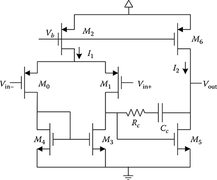
FIGURE 2.14 Two-stage op amp used in dual-slope ADC.
2.3.5.2 Thermal and Flicker Noise
Op amp transistor sizes and bias currents, shown in Table 2.1, are mainly chosen to minimize thermal and flicker noise. Reduction of the latter noise component is especially important in CV measurements because these are carried out at relatively low frequencies. The input-referred flicker noise voltage of the op amp with power spectral density (PSD)
2.21 |
where:
Cox | is the transistor gate capacitance per unit area |
f | is frequency |
Kfp and Kfn | are the technology-dependent flicker-noise constants of the PMOS and NMOS transistors, respectively |
W and L | are the transistor width and channel length, respectively |
μn and μp | are the carrier mobilities of the NMOS and PMOS transistors, respectively. |
Table 2.1 Component Values and Bias Currents for Two-Stage Op Amp Used in ADC Integrator

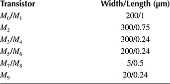
As shown in the above equation, reducing the flicker noise necessarily involves using large-area input devices. As a result, the input devices M0 and M1 in the op amp have a width and length of 4 mm and 1 μm, respectively. In addition, PMOS transistors are used as the input devices because these are known to exhibit less flicker noise than NMOS transistors [89].
Ignoring the effect of the compensation resistor and capacitor Rc and Cc, respectively, the input-referred thermal noise voltage of the op amp with PSD
2.22 |
where:
gm and ro | are the small-signal transconductance and output resistance of each transistor, respectively |
the || | symbol denotes parallel connection |
As the equation suggests, reducing the thermal noise necessarily involves maximizing the value of gm1. To this end, a bias current of 1 mA is designed to flow through M1, providing a gm1 of about 14 mS.
Simulation of the op amp input-referred noise using typical process parameters indicates an overall flicker-noise constant Kf of 1.4 × 10⁻¹² V2 and a flicker-noise corner at around 700 kHz. The thermal noise power spectral density (PSD) is about 4.0 × 10⁻¹⁸ V2 Hz–1. The total integrated noise of the op amp over a bandwidth extending from 1 Hz to 1 MHz is approximately 4.5 μVrms. The effect of this on the sensor detection limit will be studied in Section 2.3.7.
2.3.5.3 Bandwidth and Stability
A 25 pF metal-insulator-metal (MIM) capacitor is used to establish the dominant pole of the op amp at 4 kHz. A 150 Ω polysilicon resistor in series with Cc establishes a left-half-plane zero at about 50 MHz. The simulated unity-gain frequency f0 of the op amp with a load capacitance of 5 pF is 109 MHz. This is roughly equal to gm1/(2πCc).
Phase margin (PM) is an important parameter in assessing the stability of a feedback loop, such as that present in the integration amplifier. A PM less than zero means that the magnitude of the loop gain is greater than unity at frequencies where feedback signals experience a phase shift of more than 180° around the loop. As a result, input and feedback signals effectively add together and are amplified, causing the output to become unstable (grow without bound). Although a PM greater than zero is necessary to ensure stability in a linear feedback system, PMs close to zero are undesirable as these lead to long settling times and ringing in the step response.
The op amp used in the integrator exhibits the worst-case PM when operated in a unity-gain configuration. This occurs during the reset phase of the dual-slope conversion cycle, during which the integration capacitor is shorted out by closing the parallel switch connected to φ1. Assuming the switch controlled by φ2, connected directly to the inverting input of the op amp, is open during the reset period, the load capacitance CL of the op amp is dominated by its own input capacitance plus the input capacitance of the comparator. The simulated PM in this case is approximately 67°.
Alternatively, if the φ2 switch is closed during reset, the impedance of the electrode–electrolyte interface directly influences the PM. As a result, a Cwe of around 1 nF in series with an Rs1 ranging from 100 Ω to 100 kΩ appears in parallel with the usual CL. Despite this, the PM remains around 67° because the additional pole and zero provided by the interfacial impedance tend to cancel one another for values of Rs1 that are comparable or above the output resistance of the second stage of the op amp. This behavior is observed in simulation for values of Rs1 greater than about 1 kΩ.
Table 2.2 summarizes some of the important simulated performance metrics of the op amp used in the ADC integrator.
2.3.5.4 Integration Capacitor
A 5 pF MIM integration capacitor is used in the two-stage op amp feedback loop. The choice of this value is mainly based on area considerations. Alternatively, a nonlinear MOS capacitor could have been used to reduce the occupied area even more. This nonlinearity would effectively be canceled by the dual-slope algorithm.
2.3.5.5 Comparator
The track-and-latch comparator following the integrator in the dual-slope ADC is shown in Figure 2.15. Transistor sizes are included in Table 2.3. In this design, transistors M5 and M6 separate the cross-coupled switching transistors at the output from the drains of input transistors M0 and M1 to reduce kickback interference. Although autozeroing can mitigate the effect of comparator offset on the digital output, M0 and M1 have a width and length of 200 and 1 μm, respectively, to reduce offset caused by mismatch between these transistors. The comparator provides more than 12 bits of resolution at an input clock frequency of 50 MHz in simulation.
Table 2.2 Simulated Performance of Two-Stage Op Amp Used in ADC Integrator
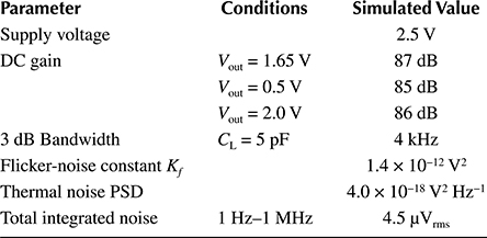

FIGURE 2.15 Track-and-latch comparator used in dual-slope ADC.
Table 2.3 Transistor Sizes for Track-and-Latch Comparator Used in Dual-Slope ADC
2.3.5.6 Current sources and switches
The devices used to source and sink current during the second integration phase of the dual-slope ADC algorithm are composed of PMOS and NMOS current mirrors, respectively, biased using off-chip resistors. The channel length of the PMOS and NMOS transistors in the switches controlled by φ3a and φ3b, respectively, are both 15 μm, while the widths are 5 and 2.5 μm, respectively. Depending on the size of the external tuning resistor, currents ranging from approximately 100 pA to 1 μA can be established.
NMOS pass transistors are used to implement the switches tied to φ1, φ2, and φ4, as these only need to pass mid-rail voltages. The latter two minimum-length switches both have a 50 μm width and exhibit a simulated on-resistance of approximately 50 Ω. The switch controlled by φ1 has a 20 μm width and an on-resistance of about 120 Ω. In addition, the switches controlled by φ1 and φ2a are connected to NMOS “dummy” switches on each side, as shown in Figure 2.11, and are clocked on alternate edges. These help reduce conversion errors caused by charge injection [21]. A 100 μm NMOS switch (not shown in Figure 2.11) is directly attached to the WE and can be used to disconnect the electrode from the sensor electronics.
2.3.5.7 Digital Counter and Control Circuitry
A digital counter is required to set t1 and measure t2 during dual-slope ADC operation. To allow sufficient range, a 20-bit ripple-carry counter is synthesized using gates from a standard-cell library. This counter can operate at frequencies exceeding 50 MHz, as verified through timing simulation.
Local digital control circuitry, implemented as a finite state machine (FSM), contains comparators to set the duration of t1 and t2,max, detects the analog comparator output, and sets the appropriate switches in the ADC to implement the dual-slope algorithm. The FSM can be bypassed and the ADC completely controlled via an external field-programmable gate array (FPGA). All analog comparator outputs are also connected to pins on the CMOS chip so that these can be observed using external benchtop measurement equipment.
2.3.6 Design of Control Amplifier Circuits
Sufficient current drive, low noise, and stability are the most important factors in the design of the control amplifier. Therefore, this component is constructed using the two-stage op amp in Figure 2.14 with the same transistor sizes as in Table 2.1. The maximum total Faradaic current expected to flow through all 16 on-chip electrodes is about 20 μA. The two-stage op amp can deliver this current easily because it is only 1% of the 2 mA second-stage bias current.
Maintaining stability over a wide range of electrolyte impedances is one of the main goals in the design of the control amplifier. The model shown in Figure 2.16 is used to study the closed-loop stability of the control amplifier when it is driving 16 identical WE–electrolyte interfaces in parallel. In circuit simulation, the feedback loop is cut and the PM is extracted from the open-loop small-signal response. To simplify the analysis, the value of Rct is assumed to be infinite, the value of Cce is assumed to be so large that its impedance is negligible over the operating frequency range, and all WEs are taken to be equal in area. In addition, the resistor Rsre has been included to model the series resistance of the highly concentrated RE filling solution (i.e., 3 M NaCl) and the RE is assumed to be placed at an equal distance from the CE and WEs so that all values of Rs are equal.
To investigate the stability range, the values of Rs and Cwe are swept from 100 Ω to 100 kΩ, and from 100 pF to 10 nF, respectively, using a parametric circuit simulation. These values are in the expected range for a modified Au electrode exposed to various concentrations of buffer. Figure 2.17 shows the PM of the open-loop ac response as a function of Rs and Cwe. As the graph in Figure 2.17 shows, the PM is above zero for all combinations of Rs and Cwe considered. It is apparent, however, that different regions of stability exist. To understand these regions better, it is useful to examine the pole and zero locations in the open-loop transfer function. For small values of Rs, the dominant fp1 and nondominant fp2 pole frequencies of the open-loop transfer function can be expressed approximately as

FIGURE 2.16 Model used to simulate closed-loop stability of the control amplifier feedback loop.
2.23 |

FIGURE 2.17 Phase margin of the control amplifier feedback loop as a function of the WE capacitance and solution resistance when 16 sensors are operating in parallel.
and
2.24 |
where:
R1 and R2 | represent the equivalent output resistances of the first and second op amp stages, respectively |
C1 and C2 | are the total transistor capacitances at the output of the first and second stages, respectively |
The WE impedances also add a zero fz to the transfer function at
2.25 |
in which the contribution from Rs has been included. In Figure 2.17, values of Cwe greater than about 500 pF, coupled with small Rs values, give PMs between 60° and 90°. This is because the zero at fz helps bring the phase shift up at higher frequencies. On the other hand, the PM declines rapidly and approaches about 35° for values of Rs greater than approximately 10 kΩ since fz is translated to lower frequencies. The rapid decline in PM for the smallest values of Rs and Cwe occurs because fz now exists well above fp2.
Not all combinations of Rs and Cwe in Figure 2.17 can be obtained experimentally. For example, it has been shown that the interfacial capacitance at an Au electrode modified with ssDNA probes changes very little even when the electrolyte concentration is varied by many orders of magnitude [90].
2.3.7 Sensor Detection Limit and Noise Analysis
The smallest DNA target coverage that can be measured by the CMOS sensor array is limited by electrochemical noise processes [91], noise from the integrated electronics, ADC quantization noise, and uncertainties arising from cross-hybridization due to nonspecific binding during operation in a multitarget analyte [92]. Since the last noise source is beyond the scope of this work, only the first three will be analyzed.
For purposes of noise modeling, the simplified circuit model of the dual-slope ADC and electrochemical interface shown in Figure 2.18 are used. The parallel resistance Rct is assumed to be infinite since the WE is normally passivated with an alkanethiol SAM, as discussed in Section 2.2.6. Also, to simplify the analysis, only the current integration period of the ADC for the duration t1 is considered. It is also assumed that all noise sources are uncorrelated and that the small-signal parameters of the electrochemical cell remain fixed over the input voltage range.
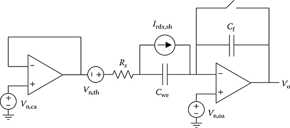
FIGURE 2.18 Simplified circuit model of the dual-slope ADC and electrochemical interface for noise analysis.
The detection limit of the active CMOS biochip can be determined by finding the target coverage ST in the redox current term iad,p in Equation 2.17 that produces an SNR of 3 at the output of the integrator. The analysis is simplified by considering only the maximum value of the redox current. The SNR of the integrator output is given by
2.26 |
The variables in the above expression are now described.
2.27 |
2.3.7.1 Integrated Noise
The integrator output voltage Vo,n produced after integration period t1 with an input noise current In(t) is given in the time domain by
2.28 |
where u(t) is the unit-step function and * represents the convolution operator.
The result can be converted to the frequency domain for noise computation as follows:
2.29 |
where
Integrating the above equation over frequency gives the average noise power after t1 as
2.30 |
2.3.7.2 Shot Noise from a Redox Current
Faradaic processes produce shot noise [91] that can be modeled as a current source, as shown in Figure 2.18. This source represents a zero-mean, wide-sense stationary (WSS), white Gaussian noise process with PSD
2.31 |
2.3.7.3 Thermal Noise from Electrolyte Resistance
Series resistance Rs1 at the WE interface generates thermal noise current with PSD
2.32 |
For an Rs1 of 275 Ω (experimentally measured using a 100 × 100 μm2 Au WE in a 1 M potassium phosphate buffer [PPB]), Cwe of 2 nF, T of 298 K, and t1 set to 15 μs, the rms noise voltage at the integrator output due to the electrolyte resistance is 810 μVrms.
2.3.7.4 Amplifier Thermal Noise
The contribution to total output noise from thermal noise produced by the integrator op amp is found using the circuit in Figure 2.18. Assuming the op amp has a single pole at the frequency f0 and a dc gain A0, its open-loop frequency response A(f) is given by
2.33 |
The average output noise power at the end of the integration period
2.34 |
Using the simulated gain, bandwidth, and noise PSD parameters for the integrator op amp in Table 2.2, the rms thermal noise voltage at the integrator output is approximately 450 μVrms.
Thermal noise produced by the control amplifier with PSD
2.35 |
Using the op amp thermal noise PSD in Table 2.2 (which is equivalent to the output-referred noise because the control amplifier operates in a unity-feedback configuration), the thermal noise contributed by the control amplifier after an integration period t1 is about 760 μVrms.
2.3.7.5 Amplifier Flicker Noise
The input-referred flicker noise of the integration amplifier has PSD
2.36 |
where Kf (with dimensions V2) is a constant related to the CMOS fabrication parameters and fmin = 1/t1 is the frequency at which the integrator is reset.
The flicker noise power at the integrator output after duration t1,
2.3.7.6 Quantization Noise
The ADC quantization noise power
2.37 |
where VΔ is the voltage difference between two adjacent quantization levels of the ADC.
Assuming VR is the linear output voltage range of the integrator op amp in the dual-slope ADC in Figure 2.11, and N is the number of bits in the counter used to measure t2 in Equation 2.20, VΔ is given by
2.38 |
As an example, VΔ is approximately 0.73 mV assuming a VR of 0.75 V and a 10-bit nominal resolution. This produces a quantization noise voltage of about 210 μVrms.
2.3.7.7 Target Coverage Detection Limit
Figure 2.19 displays the contributions from each of the noise sources discussed above (except for quantization noise) as a function of DNA surface target coverage. The total noise at the integrator output for an integration period lasting 15 μs stays approximately constant at 1.3 mVrms. As can be seen, the thermal noise generated by the electrochemical cell resistance, integration op amp, and control amplifier dominates the total sensor noise.
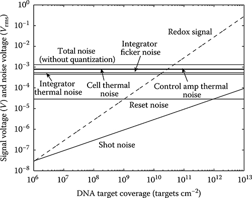
FIGURE 2.19 Signal voltage and noise voltages at the integrator output as a function of DNA surface target coverage.
The quantization-noise-free SNR given by Equation 2.26 (but excluding the
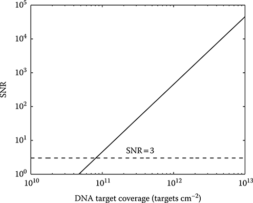
FIGURE 2.20 Quantization-noise-free SNR as a function of DNA surface target coverage.
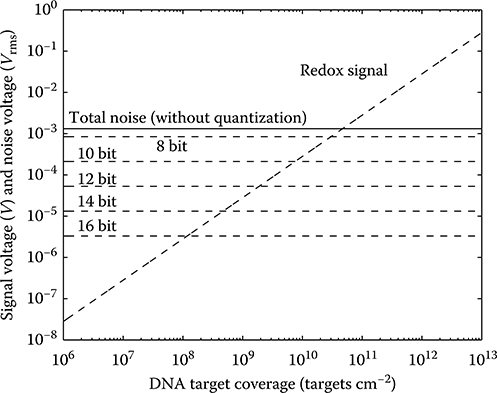
FIGURE 2.21 Quantization noise voltage for different ADC resolutions along with the quantization-free noise level at the integrator output.
Figure 2.21 shows the quantization-free noise voltage determined above as well as the quantization-noise level for different ADC resolutions, assuming a VR of 0.75 V. It is evident that quantization noise at levels of 10 bits or more does not contribute significantly to the total noise at the integrator output. The minimum target coverage that can be detected with an SNR of 3 using an 8-, 10-, and 12-bit ADC is 9.6 × 10¹⁰, 8.2 × 10¹⁰, and 8.0 × 10¹⁰ targets cm–2, respectively.
It is also useful to study the effect of WE area and ADC integration time on the DNA target detection limit of the sensor. Analysis of these is carried out below.
2.3.7.8 Effect of Working Electrode Area on Detection Limit
Figure 2.22 shows the sensor detection limit as a function of the WE area. The detection limit decreases as the WE area increases because the redox signal power goes up with the square of the area, while the thermal noise power produced by Rs and the control amplifier increases by a smaller factor.
2.3.7.9 Effect of ADC Integration Time on Detection Limit
Increasing the duration t1 over which the ADC integrates the WE current has the effect of reducing the sensor detection limit, as displayed in Figure 2.23a. This is again due to the power-of-two relationship between the maximum redox current level and overall signal power. However, this analysis assumes that the CV scan rate remains unchanged. Using a long t1 means that the ADC sample rate must be reduced, assuming a constant Iref. Therefore, fewer points on the CV curve can be collected when both t1 and V are large. This, in turn, reduces the accuracy associated with integrating the WE current to obtain the total charge transferred. In addition, as the scan rate increases, so does the charging current in proportion. As a result, saturation occurs when the sum of the redox signal and charging currents produces a voltage outside the linear range of the integrator op amp. This is evident when t1 is equal to 30 μs in Figure 2.23b. For longer integration periods, saturation can occur before the SNR even reaches 3.

FIGURE 2.22 Effect of working electrode area on sensor target coverage detection limit.
2.3.7.10 Sensor Dynamic Range
The sensor DR is defined as the ratio of the largest nonsaturating input current Imax to the minimum detectable input current Imin. These are given by the following expressions:
2.39 |
2.40 |
where Vo,max is the maximum linear output voltage of the integrator op amp. The DR can therefore be expressed as
2.41 |
Assuming a VR of 0.75 V and a t1 of 15 μs, the DR of the sensor as a function of the surface target coverage stays fairly constant at around 520, which is equivalent to about 2.8 decades.

FIGURE 2.23 Effect of ADC integration time t1 on sensor detection limit. (a) Sensor limit of detection as a function of integration time. (b) SNR for various integration times. Saturation occurs when the sum of the redox signal and charging currents produce a voltage outside the linear range of the integrator op amp.
2.3.8 CMOS Biochip Fabrication and Postprocessing
The electrochemical DNA biochip is fabricated in a Taiwan Semiconductor Manufacturing Company (TSMC, Hsinchu, Taiwan) 2.5 V, five-metal, 0.25 μm, mixed-signal CMOS process. All five metal layers in this process are made of Al. A photograph of the 5 × 3 mm2 die is shown in Figure 2.24. Each of the 16 sensor sites on the chip, comprised of a WE and dual-slope ADC, measures approximately 650 × 350 μm2. About two-thirds of this area is occupied by the two-stage integrator op amp and compensation capacitor. Each of the control amplifiers occupies an area of about 400 × 400 μm2, while the amplifiers in the diagnostic circuits use less than 350 × 350 μm2 of silicon area.
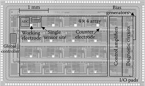
FIGURE 2.24 Die photograph of the active CMOS sensor array for label-based electrochemical DNA assays.
At the time of chip physical design, pads in the top metal layer (M5) are laid out to form the integrated WEs and CEs. Tungsten (W) vias vertically connect M5 to the other Al metal layers below. Openings are then specified in the 1–2 μm thick silicon nitride (Si3N4) and SiO2 passivation layers above the WE and CE metal pads, as shown in Figure 2.25, exposing the top Al metal at these locations. This process is no different from that used to construct bond pads along the chip perimeter.
Postprocessing of the fabricated CMOS chip is necessary to create an array of Au electrodes on the surface at the predefined locations discussed previously. As was described in Section 2.2.6, Au has the advantages of being relatively electrochemically inactive in the presence of strong electrolytes and is easily modified by self-assembly of well-ordered monolayers of thiol, sulfide, or disulfide compounds through Au–S bonding.
2.3.8.1 Initial Electrode Fabrication Procedure
Gold electrodes are constructed on the CMOS surface using standard microfabrication techniques in a clean-room environment at Columbia University. Gold is used for both the WEs and CEs in order to reduce the number of processing steps. Originally, a 20 nm thick layer of titanium (Ti) was deposited using electron-beam (e-beam) evaporation under vacuum directly onto the Al metal pads to act as an adhesion layer, followed by a 200–300 nm thick layer of Au using the same technique. Standard photolithographic techniques were employed to selectively cover the chip with photoresist in order to lift off deposited metal at undesired locations following evaporation. After postprocessing, the chip layer stack appears as shown in Figure 2.26a, while Figure 2.26b shows an optical microscope image of a WE and CE.
Unfortunately, depositing Ti/Au directly onto Al pads causes corrosion problems when the chip is operated in a wet electrochemical environment. This is because Al, unlike Au, is highly electrochemically active and corrodes easily when exposed to an electrolyte. During experiments in which the CMOS chip was operated in an analyte solution (to be discussed in greater detail in Section 2.4), it is thought that dissolved ions, such as chloride, penetrate the Ti/Au through grain boundaries in the thin-film layers. Following penetration, it is believed that the Al pad below reacts with the ions, corroding after only a short time. When this occurs, the Ti/Au film is destroyed as well, as can be seen in Figure 2.27.
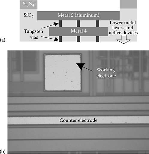
FIGURE 2.25 CMOS biochip Al metal layers with the passivation removed. (a) Layer stack-up showing the two highest Al metal layers (not to scale). (b) Optical photograph of the top metal layer of the CMOS biochip at a WE site with the passivation removed.
2.3.8.2 Improved Electrode Fabrication Procedure
To eliminate the corrosion problem and subsequent destruction of the WEs and CEs, the Al is selectively removed at the electrode locations prior to Ti/Au deposition, as shown in Figure 2.28a. This is done using a phosphoric acid–based wet etchant from Transene (Aluminum Etchant Type A). After Al removal, the Ti/Au layers are e-beam evaporated onto the electrode locations, as displayed in Figure 2.28b. The added metal electrically connects to the lower metal layers through the existing W vias.
Figure 2.29 shows an optical microscope image of a WE site following Al etching. The dense grid of W vias is clearly visible, along with the fourth Al metal layer. Therefore, evaporated metal can easily make a solid electrical connection to the via during deposition.
The advantages of the above electrode fabrication method are that it is both simple and inexpensive. For instance, it does not require an entire back-end process as in [75]. In addition, it needs fewer processing steps than when constructing a “stepped” electrode structure in which the Au electrode is built adjacent to, rather than directly above, an Al pad [93]. Furthermore, only a few inexpensive ingredients are required to prepare the Al etchant, which is fully compatible with standard photolithographic processes.
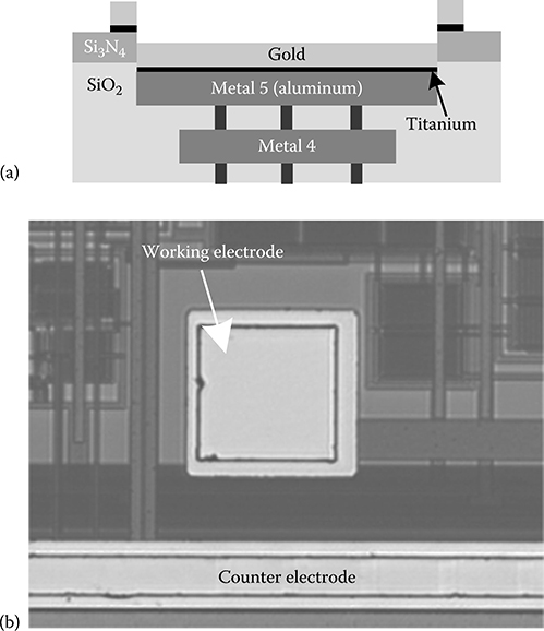
FIGURE 2.26 Original postprocessing method used to construct Au electrodes on the surface of the CMOS biochip. (a) Chip layer stack-up after Ti/Au is deposited directly on the native Al pads. (b) Optical microscope image of a WE and CE after postprocessing.

FIGURE 2.27 Visible destruction of an integrated WE and CE after the CMOS biochip is operated in an electrolyte.
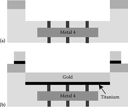
FIGURE 2.28 Improved electrode fabrication procedure. (a) Aluminum at electrode sites is selectively etched away using standard photolithographic techniques. (b) Titanium and Au are deposited onto the electrode sites and electrically connect to the metal layers below through the existing vias.
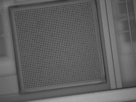
FIGURE 2.29 A working electrode site following Al removal using a wet etch.
2.4 Experimental Results
Experimental results are presented in this section that validate the operation of the active CMOS biochip for label-based electrochemical DNA assays. Biochip packaging issues, results from electrical characterization, and integrated electrochemical measurements of redox species and ferrocene-labeled DNA targets are described in detail.
2.4.1 CMOS Chip Packaging and Experimental Setup
To enable electronic characterization, electrochemical testing, and external interfacing of the active CMOS biochip, the chip is mounted in a 272-pin, 27 × 27 mm2 ball grid array (BGA) package with its surface partially exposed, as displayed in Figure 2.30. The metal bond wires connecting the input and output (I/O) pads along the chip perimeter to pads on the BGA package are encapsulated using a heat-cured, chemical-resistant epoxy (Hysol, Henkel, Düsseldorf, Germany) to protect them from electrolyte exposure. Bonding and packaging of the CMOS chips are performed by an external vendor (Corwil, Milpitas, CA).
The packaged chip is fastened in a surface-mount socket on a custom-designed printed circuit board (PCB) using a top plate provided by the socket vendor. A square, 1 mm thick poly(dimethylsiloxane) (PDMS) sheet having a square hole cut out in the center to leave the chip surface uncovered is sandwiched between the chip package and top plate. The PDMS essentially acts like a gasket, preventing analyte leakage onto the PCB. A glass tube is attached to the top plate using an ultraviolet (UV)-cured epoxy to form a 12 mL analyte reservoir over the chip. An external Ag/AgCl/3 M NaCl RE is held in the reservoir with a Teflon cap.
2.4.2 Electrical Characterization
Electrical characterization of the active CMOS biochip is carried out prior to performing integrated electrochemical measurements. Figure 2.31 shows the output noise spectrum of the control amplifier over a bandwidth from 10 Hz to 21 kHz when this device is operated in a unity-gain configuration. The 1/f corner frequency is located above the maximum input frequency of the spectrum analyzer. The measured output noise voltage is 21.2 μVrms over the 10 Hz–21 kHz band when the effect of 60 Hz line interference and other interfering tones is removed.
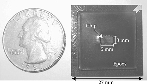
FIGURE 2.30 Packaged CMOS biochip in which the bond wires are covered using a chemical-resistant epoxy to protect them from analyte exposure. The US quarter dollar is included for size comparison.
Characterization of the dual-slope ADC at each sensor site is carried out using the on-chip diagnostic circuits. To allow sufficient bandwidth for CV experiments, the ADCs are operated at a sampling rate fs of 2.5 kHz with φclk set to 3.5 MHz. The first integration time t1 is set to 23 μs and t2,max is 315 μs, providing a nominal resolution of 10 bits (plus an additional sign bit). Although dual-slope ADCs generally feature resolutions of 16 bits or more, these are normally operated at very low sampling rates (a few hertz) to avoid use of an impractically high value of φclk. For the current application, resolution has been traded off so that a higher sampling rate could be employed. In addition, use of a lower-speed φclk reduces the level of on-chip switching interference that can couple into the analog circuit blocks.
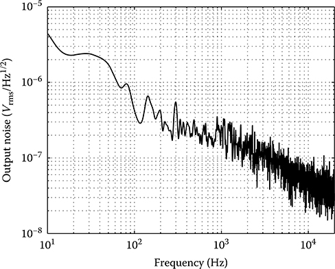
FIGURE 2.31 Output noise spectrum of the control amplifier from 10 Hz to 21 kHz with interference tones removed.
The remaining time during each conversion cycle is required to reset Cf and select the appropriate reference current source. The maximum Iwe before integrator saturation using these settings is about 110 nA. Reference currents Iref+ and Iref– are set to 15 and 18 nA, respectively. Typical differential nonlinearity (DNL) and integral nonlinearity (INL) values for the ADCs are –0.25 and +0.38 LSB, respectively, with an LSB current of approximately 240 pA.
The DR of the ADC is experimentally verified using a 103 Hz sinusoidal input current. Figure 2.32a displays the typical SNR and signal-to-noise-and-distortion ratio (SNDR) of the ADC as a function of input current level. The lower end of the DR curve is fitted due to the difficulty in providing a sufficiently small ac voltage signal to the on-chip transconductance amplifiers used for ADC testing. The DR is limited at the upper end by integrator saturation. A maximum effective number of bits (ENOB) of 9 is achieved and is limited by the linearity of the test circuits. A DR greater than 10 bits is achieved from circuit simulations of the dual-slope ADC alone. Figure 2.32b shows the result of an 8192-point fast Fourier transform (FFT) of the measured ADC output when a full-scale input is applied. The strong second harmonic is due to the single-ended architecture of the ADC.

FIGURE 2.32 Typical measured results from ac linearity testing of the dual-slope ADCs. (a) Dynamic range. (b) Output spectrum with a full-scale input at 103 Hz. The resolution bandwidth is 0.31 Hz.
2.4.3 Integrated Electrochemical Measurements of a Bulk Redox Species
As a first example of the use of the active CMOS biochip for basic electrochemical sensing, CV measurements of the bulk redox species potassium ferricyanide, K3[Fe(CN)6], are carried out. At the appropriate potential, ferricyanide ions are reduced to ferrocyanide ions in the reaction
2.42 |
Potassium ferricyanide is often used by electrochemists to study interfacial properties because of its highly reversible behavior. It is for this reason also that potassium ferricyanide is often used as a diagnostic measurement tool in electrochemical systems.
2.4.3.1 Biochip Preparation and Experimental Procedure
In order to demonstrate proper functioning of the active CMOS biochip, CV measurements of 2 mM potassium ferricyanide in 1 M PPB (pH 7.4), made by combining appropriate amounts of K2HPO4 and KH2PO4 in water, are carried out. In these experiments, the potential between all the WEs in the array (held at 1.25 V relative to ground) and RE is scanned from +0.75 to –0.5 V and back at various rates while the cell current is observed at one WE. To extend the potential range of the electrochemical cell beyond the 2.5 V power supply limit, the on-chip control amplifiers are bypassed and a discrete, off-chip op amp (AD8628, Analog Devices, Norwood, MA), operating at 3 V, is used to drive an external Pt-wire CE rather than the on-chip Au WEs. A standard Ag/AgCl/3 M NaCl RE (RE-5B, Bioanalytical Systems, West Lafayette, IN) is used in all experiments.
Cleaning of the WE surface is necessary to avoid contamination from one experiment to the next. This is particularly important when performing DNA sensing because probe layers left over from previous experiments affect the hybridization thermodynamics of subsequent studies. Thick, macroscopic Au electrodes can be easily cleaned through mechanical polishing or controlled dissolution through voltage cycling in a strong acid and oxidizing agent. However, such techniques are too invasive and impractical to be applied to the thin-film Au WEs on the CMOS biochip. Therefore, before each new experiment, the chip is placed in a UV/ozone cleaner for 5 min to break down organic contaminants on the Au WE surfaces [94]. These can then be eliminated from the surface by thorough rinsing in deionized water.
2.4.3.2 Measurement Results
Figure 2.33a shows the cell current at one of the 100 × 100 μm2 WEs when an input scan rate v of 72 mV s–1 is used. A zero-phase, low-pass FIR filter is used to postprocess the raw data in MATLAB®. The locations of the forward (reduction) and reverse (oxidation) current peaks at +0.22 and +0.30 V, respectively, match those obtained when the same experiment is run on a commercial potentiostat using a 125 μm diameter Au WE. In addition, the 80 mV difference in the potentials at which the maximum forward and reverse currents occur (also known as the “peak potentials”) is relatively close to the theoretical value of 59 mV for a fully reversible, single-electron redox process given by Equation 2.11. The magnitude of the current falls after each peak due to mass-transport limitations of the redox species to the WE surface.
In Figure 2.33b, v is increased from 24 to 480 mV s–1 and the peak reduction current is measured. As indicated by the Randles–Sevcik equation (Equation 2.10), the peak current ip at a planar electrode for a reversible reaction under diffusive control (measured after subtracting the charging current background) increases linearly with v1/2. This behavior is observed in Figure 2.33b.

FIGURE 2.33 CV measurements of the bulk redox species potassium ferricyanide using the active CMOS biochip. (a) Measured result at a 100 × 100 μm2 WE at a scan rate of 72 mV s–1. (b) Peak current dependence of ferricyanide reduction on scan rate.
The linear dependence of ip on WE area (also reflected in Equation 2.10) is also verified by running a CV scan at 290 mV s–1 and observing the current flowing through the 100 × 100, 90 × 90, and 80 × 80 μm2 WEs. Figure 2.34 shows the results from this measurement. The actual WE area is assumed to be 1.5 times greater than the geometric (drawn) area in order to account for surface roughness of the e-beam-deposited Ti/Au layer. This value is in the range measured in independent, off-chip experiments on Au electrodes and has been verified by others for evaporated thin-film metals [95].
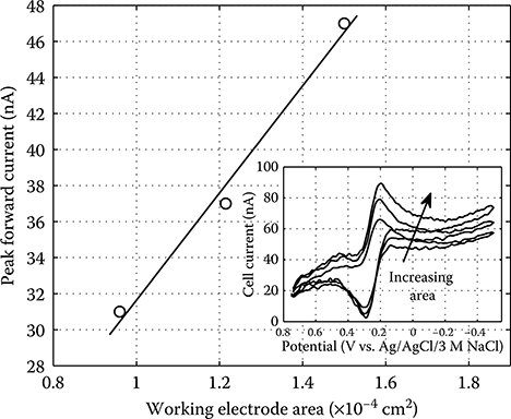
FIGURE 2.34 Dependence of peak current from ferricyanide reduction on the WE area.
2.4.4 Integrated Electrochemical Measurement of DNA Probe Surface Coverage
This section describes the use of the active CMOS biochip in determining the coverage of ssDNA probes on the WE surface. As outlined in Section 2.2.3, knowledge of the ssDNA probe surface coverage is necessary in order to calculate thermodynamic parameters in affinity-based DNA sensing assays.
In these experiments, Au WEs are functionalized with a monolayer of ssDNA probes and CV measurements are then carried out in the presence of the redox intercalator hexaamineruthenium(III) chloride to determine probe surface density. The redox-active counterion RuHex3+ associates with the surface-immobilized DNA, causing the thermodynamics of the redox processes to be altered. Prior work has shown that as probe coverage increases, the reduction potential for the reaction
2.43 |
shifts toward more negative values. This phenomenon is due, in part, to changes in local dielectric constant, spatial distribution, and solvation [90]. This technique can provide an absolute measure of the probe coverage once calibration using a surface-analysis technique such as x-ray photoelectron spectroscopy (XPS) has been carried out.
2.4.4.1 Biochip Preparation and Experimental Procedure
The chip is cleaned as described previously and is then incubated for 30 min in a 1 M MgCl2 solution containing a known concentration of thiolated, 20-mer ssDNA probe having the sequence 5′-TTT TTT TCC TTC CTT TTT TT-3′. Next, the chip is incubated in 1 mM mercaptopropanol (MCP) solution for 90 min, forming a SAM that helps to passivate the WE surface and prevent nonspecific interactions between the immobilized DNA and WE, as was discussed in Section 2.2.6. CV at a scan rate of 4 V s–1 is then carried out in 7 mL of 10 mM Tris acetate buffer (pH 7.4) with 1 μM RuHex3+.
2.4.4.2 Measurement Results
Figure 2.35 displays the results from two different CV experiments at one 90 × 90 μm2 WE for DNA probe coverages of 1 × 10¹³ and 4 × 1012 cm–2. These probe densities are obtained by incubating the chip in different concentrations of DNA probe solution (75 and 25 μM, respectively) and are verified using a set of calibration measurements on a commercial potentiostat and a 125 μm diameter Au WE. The overall shape of the CV curves is different from those obtained in the previous section because RuHex3+ electrostatically associates with the ssDNA probes at the WE surface and is, therefore, not subject to mass-transport limitations.
The forward peaks occur at –277.2 and –294.8 mV for the lower and higher probe coverage, respectively. This indicates a shift of 17.6 mV toward more negative potentials with the higher coverage, confirming previous observations. Parallel experiments on a commercial potentiostat show similar peak potentials and a closely matching shift of 15.4 mV. In addition, the quantity of RuHex3+ near the WE increases with higher probe coverage [90], as is evident in the observed peak-current increase for the 1 × 1013 cm–2 measurement.
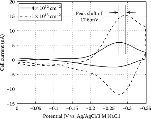
FIGURE 2.35 DNA probe surface coverage measurements using the redox intercalator RuHex3+ and the active CMOS biochip.
2.4.5 Label-Based Electrochemical DNA Sensing
Results from quantitative, multiplexed, and real-time electrochemical DNA sensing using the active CMOS biochip are now presented. The measurement technique described in Section 2.3.1, in which ssDNA targets conjugated with Fc redox labels hybridize with surface-immobilized ssDNA probes, is employed.
2.4.5.1 ADC Operation
Due to the high CV scan rate used in the current experiments (60 V s–2), the sampling rates of the integrated dual-slope ADCs are increased to 10 kHz with a φclk of 3.5 MHz. The values of t1 and t2,max are 15 and 63 μs, respectively, providing a nominal resolution of almost 8 bits (plus a sign bit). Both reference current sources are set to 60 nA. With these settings, the typical measured SNDR of the ADCs is 43.7 dB at an input current level of 38 nArms (corresponding to –6 dBFS). The typical maximum DNL and INL are +0.22 and +0.15 LSB, respectively.
2.4.5.2 Chemical Preparation
2.4.5.2.1 DNA Oligonucleotide Sequences
The sequences of the 3′-end thiolated 20-mer DNA oligonucleotide probes (MWG-Biotech, High Point, NC) and 18-mer Fc-conjugated DNA targets used in the active CMOS biochip experiments are shown in Table 2.4. The sequences for probe P1 (from Homo sapiens retinoblastoma 1 mRNA, which gives rise to a rare form of eye cancer in humans) and target T1, and P2 and T2, are pairwise complementary, respectively. The sequence of target T1s differs from that of T1 by a single base. These model sequences are selected in order to demonstrate the functionality of the active CMOS biochip and to allow comparison with off-chip electrochemical experiments with a commercial benchtop potentiostat using the same DNA sequences. Methods to prepare the N-(2-ferrocene-ethyl) maleimide redox label and perform target DNA conjugation can be found in [25].
Table 2.4 DNA Oligonucleotide Sequences Used in Label-Based DNA Sensing Experiments
2.4.5.3 Chip Surface Preparation
The surface of the CMOS chip is cleaned as described previously and then incubated in a 1 MgCl2 solution containing 500 nM ssDNA probe for 30 min. This provides a probe surface density of approximately 8 × 1012 cm–2, which is determined from a set of calibration measurements performed off chip [82]. After probe immobilization, the chip is incubated in a 1 mM MCP solution for 90 min. All CV experiments are run using 7 mL of 1 M PPB (pH 7.4).
2.4.5.4 Measurement Results
2.4.5.4.1 Basic DNA Hybridization Detection
Figure 2.36 shows a typical output from the ADC measured at one of the 100 × 100 μm2 WEs in the array, functionalized with probe P1, approximately 50 min after 50 nM of target T1 is introduced to the system. The current peaks due to the Fc redox reactions are evident above the charging current level, indicating hybridization between P1 and T1. Hysteresis causes the forward and reverse charging currents to differ somewhat. Based on the average charging current, the WE interfacial capacitance is measured to be approximately 7 μF cm–2, which is in the expected range for an MCP-modified Au electrode at the DNA coverage and buffer ionic strength used [90].
Figure 2.37 indicates that the peak current level (average of forward and reverse peaks after background subtraction) increases linearly with scan rate, as predicted by theory for a surface redox species (see Equation 2.12). This confirms that the signal current originates from surface-hybridized DNA targets and not diffusing species in solution. Additionally, the measured linear dependence of peak current on WE area, as predicted by theory, is shown in Figure 2.38.
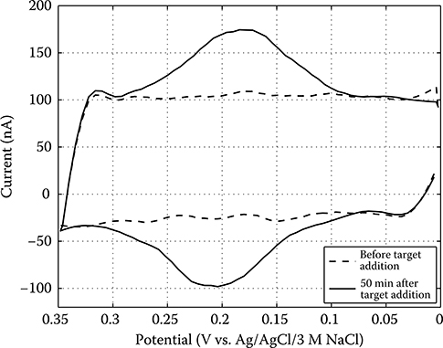
FIGURE 2.36 A typical CV measurement using the active CMOS biochip in which the charging current, observed before complementary DNA target is added to the analyte, is shown along with the sensor response from hybridization, 50 min after target addition, at one 100 × 100 μm2 WE.
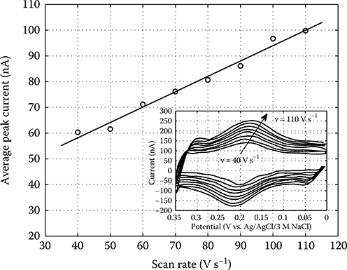
FIGURE 2.37 Linear dependence of the average peak current (after background subtraction) on the CV scan rate. Inset shows the resulting waveform from each scan.

FIGURE 2.38 Linear dependence of the average peak current (after background subtraction) on the WE area. Inset shows the resulting waveform from each scan.
2.4.5.4.2 DNA Target Concentration Series
The active CMOS biochip enables real-time quantitation of surface-hybridized targets in a multiplexed fashion. This, in turn, allows large-scale optimization of parameters affecting hybridization in diagnostic assays including probe coverage, target concentration, probe and target sequence, buffer ionic strength, and temperature [41]. As a first step in this direction, it is important to examine the relationship between the concentration of DNA target in solution and the magnitude of the sensor output signal.
FIGURE 2.39 Results of a DNA target concentration, measured at one 100 × 100 μm2 WE, in which the hybridization extent x is plotted as a function of the solution target concentration. The dashed line is the Langmuir fit to the measured equilibrium isotherm. Errors bars for the four lowest target concentrations indicate the standard deviation from three separate experiments.
Figure 2.39 displays the results of a target concentration series, measured at one 100 × 100 μm2 WE, in which the extent of hybridization x = ST/SP, is plotted as a function of the solution target concentration. By fitting the measured data in the figure according to Equation 2.3, Ka is found to be approximately 1 × 10⁸ M–1. This value of Ka falls in the range determined in previous studies of surface-based DNA sensing assays (107–109 M–1) [41].
Measurement of the standard deviation of the charging current background in Figure 2.36 provides some indication of the experimental detection limit of the sensor. With a measured standard deviation of approximately 2.1 nA (or, equivalently, a current noise variance of 4.4 × 10⁻¹⁸ A2), the smallest target coverage that could be measured with an SNR of 3 is about 3.9 × 10¹¹ targets cm–2, based on solving for ST in the redox current term in Equation 2.17. This value is about five times larger than the theoretical limit found in Section 2.3.7.7 using a 9-bit ADC. This discrepancy may be due to the fact that the additional noise from the second integration phase of the dual-slope ADC was neglected in the analysis in addition to the flicker noise contribution from the control amplifier.
2.4.5.4.3 Real-Time DNA Sensing
Figure 2.40 demonstrates observation of DNA probe–target hybridization in real time when 60 nM of T1 is hybridized to complementary P1 at one of the 100 × 100 μm2 WEs. In the figure, a CV scan is made every 5 min with the cell potential held at 0 V between scans. An increase in the area of the redox target signal is evident over time. Although equilibrium has not been reached after 35 min in the figure, it is expected that the maximum extent of hybridization will be about 7.0 × 1012 cm–2.
Real-time detection permits the study of DNA hybridization kinetics, which is not possible using traditional fluorescence-based DNA microarrays. In addition, it may be possible to predict the extent of hybridization at equilibrium before this point is actually reached experimentally. This could significantly reduce the waiting period before readout, which is of great benefit to time-critical POC diagnostic applications.
FIGURE 2.40 Real-time sensing of DNA hybridization at one 100 × 100 μm2 WE in which a CV scan is run every 5 min. The measured data are fit to a first-order rate equation (dashed line) following Langmuir kinetics. Inset shows the results from each CV scan over time.
The hybridization kinetics based on the data in Figure 2.40 are determined by ignoring mass-transport limitations, the effects of finite reaction volume, and interactions among surface sites, and by assuming that no DNA probes have hybridized at time t = 0. Therefore, the coverage of DNA duplexes on the WE surface as a function of time ST(t) can be expressed as [48]
2.44 |
The time constant τ over which the system reaches equilibrium is given by
2.45 |
where Ka = kf/kr.
Performing a nonlinear, least-squares fit of the real-time curve using Equations 2.44 and 2.45 (also plotted in Figure 2.40) gives a τ of about 590 s. From this and the value of Ka determined previously, kf and kr are calculated to be 2.4 × 10⁴ M–1 s–1 and 2.4 × 10⁻⁴ s–1, respectively. These forward and reverse rate constants fall in the same order of magnitude as those observed by others using QCM [96] and surface plasmon fluorescence spectroscopy [97]. However, the Ka measured here is relatively smaller, most likely because avidin–biotin spacers are used for probe immobilization in the referenced works.
2.4.5.4.4 Genetic Mutation Detection
Sensor specificity in the presence of SNPs is important when screening for genetic mutations that could give rise to human disease. Figure 2.41 displays the results of two separate experiments in which the same density of P1 is immobilized on a 100 × 100 μm2 WE. In the first experiment, P1 is hybridized to 6 nM of the fully complementary T1, and in the second, P1 is hybridized to the same concentration of T1s. Since the latter target is one base shy of having full complementarity with P1, these ssDNA molecules have less affinity for one another compared with that of T1 for P1. As a result, fewer T1s targets hybridize to P1.
This can be easily seen in Figure 2.41, in which the peak current level for the fully complementary target is noticeably higher than that for the target with an SNP, when both are measured at equilibrium after 60 min following target addition. In the former case, the surface target coverage is approximately 3.0 × 1012 cm–2, whereas it is about 1.6 × 1012 cm–2 in the latter. This demonstrates the use of the active CMOS biochip for genetic mutation detection.
2.4.5.4.5 Multiplexed and Specific DNA Detection
Multiplexed and specific DNA sensing using the active CMOS biochip is carried out by functionalizing the chip with two distinct probes and then hybridizing each with its complementary target. Probes P1 and P2 are spotted on four different WEs, each using a fluid microinjection system (IM-300, Narishige, East Meadow, NY) capable of delivering nL volumes of probe solution to the electrode surface.
FIGURE 2.41 Detection of fully complementary target using the active CMOS biochip and that possessing a single-nucleotide polymorphism compared with the probe.
Initially, 6 nM of target T1 is introduced, and Figure 2.42 shows the response at one of the 100 × 100 μm2 WEs functionalized with P1 (denoted “site A”) after 60 min. A distinct current peak can be seen, indicating that hybridization has occurred. The remaining WEs functionalized with P1 show similar behavior. Conversely, those WEs on which P2 is immobilized do not exhibit a hybridization signal, as P2 and T1 have little affinity for one another. The output from the sensor at one of the 100 × 100 μm2 WEs functionalized with P2 (denoted “site B”) is also displayed in Figure 2.42. Next, 6 nM of target T2 is introduced. After 55 min, the hybridization signal at site B is evident, as shown in the figure. The signal at site A (measured at the same time) has not changed, however, since T1 is still present in solution. A separate experiment confirmed that sites functionalized with P1 do not exhibit any hybridization when T2 is added to the buffer first. Figure 2.42 also shows the measured target coverage at sites A and B in real time. The values of τ for the hybridization processes are approximately 540 and 740 s at site A and B, respectively. The slight shift of the data relative to the origin is attributed to mass-transport limitations of targets to the WE surface at the beginning of hybridization. These data demonstrate that the active CMOS biochip is capable of performing real-time monitoring of DNA hybridization in a multiplexed fashion.
FIGURE 2.42 Demonstration of real-time, multiplexed, and specific DNA detection using the active CMOS biochip.
2.4.5.4.6 Surface Heating Effects
Excessive heating of the WE surfaces on the active CMOS biochip could significantly reduce the extent of hybridization observed. The amount of heating is determined by such factors as the total power consumption of the biochip, chip packaging, and the volume of fluid in the reservoir. Temperature measurement of the analyte buffer, just above the chip surface, when all 16 sensor sites are operating simultaneously reveals an increase of about 3.5°C above the quiescent temperature (≈28°C). However, even with this increase, the absolute temperature is well below the melting temperature of the various DNA strands used (≈40°C).
2.5 Summary
Active CMOS-integrated electrochemical biochips are an enabling technology in the development of genetic diagnostic platforms for clinical and POC medical applications. This chapter presented a CMOS biochip intended for use in these diagnostic systems. The biochip contained an on-chip 4 × 4 array of postprocessed Au WEs, each connected to a dual-slope ADC, and integrated potentiostat electronics to perform quantitative, multiplexed, and specific DNA sensing in real time using ferrocene-conjugated ssDNA targets. Extensive measurement results involving real-time electrochemical DNA detection demonstrated the proper functioning of this device.
References
1. J. Shendure, R. D. Mitra, C. Varma, and G. M. Church, Advanced sequencing technologies: Methods and goals, Nature Reviews. Genetics, 5, 335–344, 2004.
2. International Human Genome Sequencing Consortium, Initial sequencing and analysis of the human genome, Nature, 409, 860–921, 2001.
3. J. C. Venter, M. D. Adams, E. W. Myers, P. W. Li, R. J. Mural, G. G. Sutton, and H. O. Smith, et al., The sequence of the human genome, Science, 291, 1304–1351, 2001.
4. R. H. Waterston, E. S. Lander, and J. E. Sulston, On the sequencing of the human genome, Proceedings of the National Academy of Sciences USA, 99(6), 3712–3716, 2002.
5. F. Sanger and A. R. Coulson, A rapid method for determining sequences in DNA by primed synthesis with DNA polymerase, Journal of Molecular Biology, 94(3), 441–448, 1975.
6. M. Ronaghi, S. Karamohamed, B. Pettersson, M. Uhlén, and P. Nyrén, Real-time DNA sequencing using detection of pyrophosphate release, Analytical Biochemistry, 242, 84–89, 1996.
7. M. Margulies, M. Egholm, W. E. Altman, S. Attiya, J. S. Bader, L. A. Bemben, J. Berka, et al., Genome sequencing in microfabricated high-density picolitre reactors, Nature, 437, 376–380, 2005.
8. J. M. Rothberg, W. Hinz, T. M. Rearick, J. Schultz, W. Mileski, M. Davey, J. H. Leamon, et al., An integrated semiconductor device enabling non-optical genome sequencing, Nature, 475(7356), 348–352, 2011.
9. F. S. Collins, M. Morgan, and A. Patrinos, The human genome project: Lessons from large-scale biology, Science, 300, 286–290, 2003.
10. J. M. Rothberg and J. H. Leamon, The development and impact of 454 sequencing, Nature Biotechnology, 26, 1117–1124, 2008.
11. M. Schena, D. Shalon, R. W. Davis, and P. O. Brown, Quantitative monitoring of gene expression patterns with a complementary DNA microarray, Science, 270, 467–470, 1995.
12. R. J. Lipshutz, D. Morris, M. Chee, E. Hubbell, M. J. Kozal, N. Shah, N. Shen, R. Yang, and S. P. A. Fodor, Using oligonucleotide probe arrays to access genetic diversity, BioTechniques, 19(3), 442–447, 1995.
13. M. Chee, R. Yang, E. Hubbell, A. Berno, X. C. Huang, D. Stern, J. Winkler, D. J. Lockhart, M. S. Morris, and S. P. A. Fodor, Accessing genetic information with high-density DNA arrays, Science, 274, 610–614, 1996.
14. X. Li, R. J. Quigg, J. Zhou, W. Gu, P. N. Rao, and E. F. Reed, Clinical utility of micro-arrays: Current status, existing challenges and future outlook, Current Genomics, 9, 466–474, 2008.
15. Microarrays find their way into the clinic, Genetic Engineering & Biotechnology News, 26(18), 2006.
16. J.-Y. Coppée, Do DNA microarrays have their future behind them? Microbes and Infection, 10, 1067–1071, 2008.
17. J. Kling, Moving diagnostics from the bench to the bedside, Nature Biotechnology, 24(8), 891–893, 2006.
18. U. A. Meyer, Pharmacogenetics and adverse drug reactions, The Lancet, 356, 1667–1671, 2000.
19. T. G. Drummond, M. G. Hill, and J. K. Barton, Electrochemical DNA sensors, Nature Biotechnology, 21(10), 1192–1199, 2003.
20. J. Wang, Electrochemical nucleic acid biosensors, Analytica Chimica Acta, 469, 63–71, 2002.
21. D. Johns and K. Martin, Analog Integrated Circuit Design. New York, NY: Wiley, 1997.
22. N. H. E. Weste and D. Harris, CMOS VLSI Design: A Circuits and Systems Perspective, 3rd edn. Boston, MA: Pearson, 2005.
23. J. Liu, B. A. Williams, R. M. Gwirtz, B. J. Wold, and S. Quake, Enhanced signals and fast nucleic acid hybridization by microfluidic chaotic mixing, Angewandte Chemie International Edition, 45, 3618–3623, 2006.
24. P. M. Levine, P. Gong, R. Levicky, and K. L. Shepard, Active CMOS sensor array for electrochemical biomolecular detection, IEEE Journal of Solid-State Circuits, 43(8), 1859–1871, 2008.
25. P. M. Levine, P. Gong, R. Levicky, and K. L. Shepard, Real-time, multiplexed electrochemical DNA detection using an active complementary metal-oxide-semiconductor biosensor array with integrated sensor electronics, Biosensors and Bioelectronics, 24(7), 1995–2001, 2009.
26. D. A. Skoog, F. J. Holler, and T. A. Nieman, Principles of Instrumental Analysis, 5th edn. Philadelphia, PA: Saunders, 1998.
27. J. S. Daniels and N. Pourmand, Label-free impedance biosensors: Opportunities and challenges, Electroanalysis, 19(12), 1239–1257, 2007.
28. M. Schena, R. A. Heller, T. P. Theriault, K. Konrad, E. Lachenmeier, and R. W. Davis, Microarrays: Biotechnology’s discovery platform for functional genomics, Trends in Biotechnology, 16(7), 301–306, 1998.
29. C. A. Harrington, C. Rosenow, and J. Retief, Monitoring gene expression using DNA microarrays, Current Opinion in Microbiology, 3, 285–291, 2000.
30. C. Debouck and P. N. Goodfellow, DNA microarrays in drug discovery and development, Nature Genetics, 21, 48–50, 1999.
31. M. J. Cunningham, Genomics and proteomics: The new millennium of drug discovery and development, Journal of Pharmacological and Toxicological Methods, 44, 291–300, 2000.
32. J. G. Hacia, Resequencing and mutational analysis using oligonucleotide microarrays, Nature Genetics, 29, 42–47, 1999.
33. P. F. Macgregor and J. A. Squire, Application of microarrays to the analysis of gene expression in cancer, Clinical Chemistry, 48(8), 1170–1177, 2002.
34. G. Gibson, Microarrays in ecology and evolution: A preview, Molecular Ecology, 11, 17–24, 2002.
35. J. K. Peeters and P. J. Van der Spek, Growing applications and advancements in microarray technology and analysis tools, Cell Biochemistry and Biophysics, 43(1), 149–166, 2005.
36. M. Schena, Microarray Analysis. Hoboken, NJ: Wiley, 2003.
37. J. Liu, S. Tian, L. Tiefenauer, P. E. Nielsen, and W. Knoll, Simultaneously amplified electrochemical and surface plasmon optical detection of DNA hybridization based on ferrocene-streptavidin conjugates, Analytical Chemistry, 77(9), 2756–2761, 2005.
38. M. R. Linford and C. E. D. Chidsey, Alkyl monolayers covalently bonded to silicon surfaces, Journal of the American Chemical Society, 115(26), 12631–12632, 1993.
39. S. P. A. Fodor, R. P. Rava, X. C. Huang, A. C. Pease, C. P. Holmes, and C. L. Adams, Multiplexed biochemical assays with biological chips, Nature, 364, 555–556, 1993.
40. G. Patounakis, Active CMOS substrates for biomolecular sensing through time-resolved fluorescence detection, PhD. Dissertation, Columbia University, New York, NY, 2005.
41. R. Levicky and A. Horgan, Physicochemical perspectives on DNA microarray and biosensor technologies, Trends in Biotechnology, 23(3), 143–149, 2005.
42. R. P. Ekins and F. W. Chu, Multianalyte microspot immunoassay: Microanalytical “compact disk” of the future, Clinical Chemistry, 37(11), 1955–1967, 1991.
43. S. Draghici, P. Khatri, A. C. Eklund, and Z. Szallasi, Reliability and reproducibility issues in DNA microarray measurements, Trends in Genetics, 22(2), 101–109, 2006.
44. Affymetrix, Affymetrix GeneChip Scanner 3000 7G Data Sheet, 2005. scanner3000_datasheet.pdf. Available at: http://www.affymetrix.com/support/technical/datasheets/.
45. Molecular Devices. (2008) Axon GenePix 4300A and 4400A Scanners.gn_genepix_4300_4400.html. Available at: http://www.moleculardevices.com/Products/Instruments/Microarray-Scanners/GenePix-43004400.html.
46. G. Bhanot, Y. Louzoun, J. Zhu, and C. DeLisi, The importance of thermodynamic equilibrium for high throughput gene expression assays, Biophysical Journal, 84, 124–135, 2003.
47. A. W. Peterson, R. J. Heaton, and R. M. Georgiadis, The effect of surface probe density on DNA hybridization, Nucleic Acids Research, 29(24), 5163–5168, 2001.
48. H. Dai, M. Meyer, S. Stepaniants, M. Ziman, and R. Stoughton, Use of hybridization kinetics for differentiating specific from non-specific binding to oligonucleotide micro-arrays, Nucleic Acids Research, 30(16), e86, 2002.
49. H. Vikalo, B. Hassibi, and A. Hassibi, A statistical model for microarrays, optimal estimation algorithms, and limits of performance, IEEE Transactions on Signal Processing, 54(6), 2444–2455, 2006.
50. J. Wang, Analytical Electrochemistry, 3rd edn. Hoboken, NJ: Wiley, 2006.
51. A. J. Bard and L. R. Faulkner, Electrochemical Methods: Fundamentals and Applications, 2nd edn. New York, NY: Wiley, 2001.
52. E. Laviron, The use of linear potential sweep voltammetry and of a.c. voltammetry for the study of the surface electrochemical reaction of strongly adsorbed systems and of redox modified electrodes, Journal of Electroanalytical Chemistry, 100, 263–270, 1979.
53. K. Hashimoto, K. Ito, and Y. Ishimori, Sequence-specific gene detection with a gold electrode modified with DNA probes and an electrochemically active dye, Analytical Chemistry, 66(21), 3830–3833, 1994.
54. A. Sassolas, D. Leca-Bouvier, and L. J. Blum, DNA biosensors and microarrays, Chemical Reviews, 108, 109–139, 2008.
55. T. M. Herne and M. J. Tarlov, Characterization of DNA probes immobilized on gold surfaces, Journal of the American Chemical Society, 119(38), 8916–8920, 1997.
56. R. Levicky, T. M. Herne, M. J. Tarlov, and S. K. Satija, Using self-assembly to control the structure of DNA monolayers on gold: A neutron reflectivity study, Journal of the American Chemical Society, 120(38), 9787–9792, 1998.
57. J. J. Gooding, Electrochemical DNA hybridization biosensors, Electroanalysis, 14(7), 1149–1156, 2002.
58. T. de Lumley-Woodyear, C. N. Campbell, and A. Heller, Direct enzyme-amplified electrical recognition of a 30-base model oligonucleotide, Journal of the American Chemical Society, 118(23), 5504–5505, 1996.
59. L. Alfonta, A. K. Singh, and I. Willner, Liposomes labeled with biotin and horseradish peroxidase: A probe for the enhanced amplification of antigen-antibody or oligonucleotide-DNA sensing processes by the precipitation of an insoluble product on electrodes, Analytical Chemistry, 73(1), 91–102, 2001.
60. J. Wang, D. Xu, A.-N. Kawde, and R. Polsky, Metal nanoparticle-based electrochemical stripping potentiometric detection of DNA hybridization, Analytical Chemistry, 71(22), 5576–5581, 2001.
61. M. Ozsoz, A. Erdem, K. Kerman, D. Ozkan, B. Tugrul, N. Topcuoglu, H. Ekren, and M. Taylan, Electrochemical genosensor based on colloidal gold nanoparticles for the detection of Factor V Leiden mutation using disposable pencil graphite electrodes, Analytical Chemistry, 75(9), 2181–2187, 2003.
62. M. Chahma, J. S. Lee, and H.-B. Kraatz, Fc-ssDNA conjugate: Electrochemical properties in a borate buffer and adsorption on gold electrode surfaces, Journal of Electroanalytical Chemistry, 567, 283–287, 2004.
63. P. He, Y. Xu, and Y. Fang, A review: Electrochemical DNA biosensors for sequence recognition, Analytical Letters, 38, 2597–2623, 2005.
64. C. Xu, P. He, and Y. Fang, Electrochemical labeled DNA probe for the detection of sequence-specific DNA, Analytica Chimica Acta, 411, 31–36, 2000.
65. C. J. Yu, Y. Wan, H. Yowato, J. Li, C. Tao, M. D. James, C. L. Tan, G. F. Blackburn, and T. J. Meade, Electronic detection of single-base mismatches in DNA with ferrocene-modified probes, Journal of the American Chemical Society, 123(45), 11155–11161, 2001.
66. R. M. Umek, S. W. Lin, J. Vielmetter, R. H. Terbrueggen, B. Irvine, C. J. Yu, J. F. Kayyem, et al., Electronic detection of nucleic acids: A versatile platform for molecular diagnostics, Journal of Molecular Diagnostics, 3(2), 73–84, 2001.
67. S. D. Vernon, D. H. Farkas, E. R. Unger, V. Chan, D. L. Miller, Y.-P. Chen, G. F. Blackburn, and W. C. Reeves, Bioelectronic DNA detection of human papillomaviruses using eSensor: A model system for detection of multiple pathogens, BMC Infectious Diseases, 3(6), 2003.
68. GenMark (2014) The eSensor® XT-8 System. Available at http://www.genmarkdx.com/products/systems/index.php.
69. J. Li, M. Xue, Z. Zhang, C. Feng, and M. Chan, A high-density conduction-based micro-DNA identification array fabricated with a CMOS compatible process, IEEE Transactions on Electron Devices, 50(10), 2165–2170, 2003.
70. Y.-T. Cheng, C.-Y. Tsai, and P.-H. Chen, Development of an integrated CMOS DNA detection biochip, Sensors and Actuators B: Chemical, 120, 758–765, 2007.
71. M. Barbaro, A. Bonfiglio, L. Raffo, A. Alessandrini, P. Facci, and I. Baràk, A CMOS fully integrated sensor for electronic detection of DNA hybridization, IEEE Electron Device Letters, 27(7), 595–597, 2006.
72. J.-K. Shin, D.-S. Kim, H.-J. Park, and G. Lim, Detection of DNA and protein molecules using an FET-type biosensor with gold as a gate metal, Electroanalysis, 16(22), 1912–1918, 2004.
73. A. L. Ghindilis, M. W. Smith, K. R. Schwarzkopf, K. M. Roth, K. Peyvan, S. B. Munro, M. J. Lodes, et al., CombiMatrix oligonucleotide arrays: Genotyping and gene expression assays employing electrochemical detection, Biosensors and Bioelectronics, 22, 1853–1860, 2007.
74. M. Schienle, C. Paulus, A. Frey, F. Hofmann, B. Holzapfl, P. Schindler-Bauer, and R. Thewes, A fully-electronic DNA sensor with 128 positions and in-pixel A/D conversion, IEEE Journal of Solid-State Circuits, 39(12), 2438–2445, 2004.
75. F. Hofmann, A. Frey, B. Holzapfl, M. Schienle, C. Paulus, P. Schindler-Bauer, D. Kuhlmeier, et al., Fully electronic DNA detection on a CMOS chip: Device and process issues, in Proceedings of the International Electron Devices Meeting, pp. 488–491, 8–11 December 2002, IEEE, Piscataway, NJ.
76. N. Gemma, S. O’uchi, H. Funaki, J. Okada, and S. Hongo, CMOS integrated DNA chip for quantitative DNA analysis, in Proceedings of the IEEE International Solid-State Circuits Conference Digest of Technical Papers, pp. 560–561, May 2006, IEEE, Piscataway, NJ.
77. A. Hassibi and T. H. Lee, A programmable electrochemical biosensor array in 0.18 μm standard CMOS, in Proceedings of the IEEE International Solid-State Circuits Conference Digest of Technical Papers, pp. 564–565, 6–10 February 2005, IEEE, Piscataway, NJ.
78. A. Hassibi and T. H. Lee, A programmable 0.18-μm CMOS electrochemical sensor microarray for biomolecular detection, IEEE Sensors Journal, 6(6), 1380–1388, 2006.
79. C. Stagni, C. Guiducci, L. Benini, B. Riccò, S. Carrara, B. Samorí, C. Paulus, M. Schienle, M. Augustyniak, and R. Thewes, CMOS DNA sensor array with integrated A/D conversion based on label-free capacitance measurement, IEEE Journal of Solid-State Circuits, 41(12), 2956–2964, 2006.
80. F. Heer, M. Keller, G. Yu, J. Janata, M. Josowicz, and A. Hierlemann, CMOS electrochemical DNA-detection array with on-chip ADC, in Proceedings of the IEEE International Solid-State Circuits Conference Digest of Technical Papers, pp. 168–169, 3–7 February 2008, IEEE, Piscataway, NJ.
81. E. Anderson, J. Daniels, H. Yu, T. Lee, and N. Pourmand, A label-free CMOS DNA microarray based on charge sensing, in Proceedings of the IEEE Instrumentation and Measurement Technology Conference Proceedings, pp. 1631–1636, 12–15 May 2008, IEEE, Piscataway, NJ.
82. P. Gong and R. Levicky, DNA surface hybridization regimes, Proceedings of the National Academy of Sciences U S A, 105(14), 5301–5306, 2008.
83. R. J. Reay, S. P. Kounaves, and G. T. A. Kovacs, An integrated CMOS potentiostat for miniaturized electroanalytical instrumentation, in Proceedings of the IEEE International Solid-State Circuits Conference Digest of Technical Papers, pp. 162–163, 16–18 February 1994, IEEE, Piscataway, NJ.
84. R. G. Kakerow, H. Kappert, E. Spiegel, and Y. Manoli, Low-power single-chip CMOS potentiostat, in Proceedings of the 8th International Conference on Solid-State Sensors and Actuators, and Eurosensors IX, pp. 142–145, 25–29 June 1995, IEEE, Piscataway, NJ.
85. M. Breten, T. Lehmann, and E. Bruun, Integrating data converters for picoampere currents from electrochemical transducers, in Proceedings of the IEEE International Symposium on Circuits and Systems, pp. 709–712, 28–31 May 2000, IEEE, Piscataway, NJ.
86. H. S. Narula and J. G. Harris, A time-based VLSI potentiostat for ion current measurements, IEEE Sensors Journal, 6(2), 239–247, 2006.
87. R. Genov, M. Stanacevic, M. Naware, G. Cauwenberghs, and N. V. Thakor, 16-Channel integrated potentiostat for distributed neurochemical sensing, IEEE Transactions on Circuits and Systems I, Fundamental Theory and Applications, 53(11), 2371–2376, 2006.
88. B. Razavi, Design of Analog CMOS Integrated Circuits. New York, NY: McGraw-Hill, 2001.
89. Y. Tsividis, Operation and Modeling of the MOS Transistor, 2nd edn. New York, NY: Oxford University Press, 1999.
90. G. Shen, N. Tercero, M. A. Gaspar, B. Varughese, K. Shepard, and R. Levicky, Charging behavior of single-stranded DNA polyelectrolyte brushes, Journal of the American Chemical Society, 128(26), 8427–8433, 2006.
91. U. Bertocci and F. Huet, Noise analysis applied to electrochemical systems, Corrosion Science, 51(2), 131–144, 1995.
92. Y. Tu, G. Stolovitzky, and U. Klein, Quantitative noise analysis for gene expression microarray experiments, Proceedings of the National Academy of Sciences USA, 99(22), 14031–14036, 2002.
93. S. M. Martin, T. D. Strong, and R. B. Brown, Monolithic liquid chemical sensing systems, in Materials Research Society Symposium Proceedings Volume 869: Materials, Integration and Technology for Monolithic Instruments, pp. 109–118, March 2005, IEEE, Piscataway, NJ.
94. J. R. Vig, UV/ozone cleaning of surfaces, Journal of Vacuum Science and Technology A, 3(3), 1027–1034, 1985.
95. S. M. Martin, CMOS-integrated liquid chemical microdetection systems, PhD. Dissertation, University of Michigan, Ann Arbor, MI, 2005.
96. Y. Okahata, M. Kawase, K. Niikura, F. Ohtake, H. Furusawa, and Y. Ebara, Kinetic measurements of DNA hybridization on an oligonucleotide-immobilized 27-MHz quartz crystal microbalance, Analytical Chemistry, 70(7), 1288–1296, 1998.
97. K. Tawa, D. Yao, and W. Knoll, Matching base-pair number dependence of the kinetics of DNA-DNA hybridization studied by surface plasmon fluorescence spectroscopy, Biosensors and Bioelectronics, 21(2), 322–329, 2005.
* DNA detection systems relying on indicator molecules are sometimes categorized as “label-free” in the literature because no chemical modification of the probes or targets is made.