
5 Technologies for Low-Cost, Hall Effect–Based Magnetic Immunosensors
CONTENTS
5.2.1 Surface Chemistry for Immobilizing an Antibody
5.2.2 Microfluidic Integration and Assay Automation
5.3 Integrated Detection for Magnetic Immunoassays
5.3.1 State-of-the-Art Methods and Limitations
5.3.2 Design of Hall Effect–Based Detectors
5.4 Sensor Design and Optimization
5.5 Magnetization-Based Hall Effect Detection
5.6 Detectors Based on Magnetic Relaxation
5.1 Introduction
Technologies for the high-sensitivity, specific detection of proteins are used routinely in a variety of laboratory tests, ranging from diagnostic tests for infectious disease detection to food integrity evaluation. In the current testing paradigm, samples are collected at the point of need and sent to a central laboratory for preprocessing and evaluation. Laboratories aggregate samples from a relatively large geographical area, and hence are able to amortize the cost of the instrumentation and personnel required to run each test by processing many samples in parallel. Today, the most common testing protocol is known as enzyme-linked immunosorbent assay (ELISA), and is summarized in Figure 5.1.
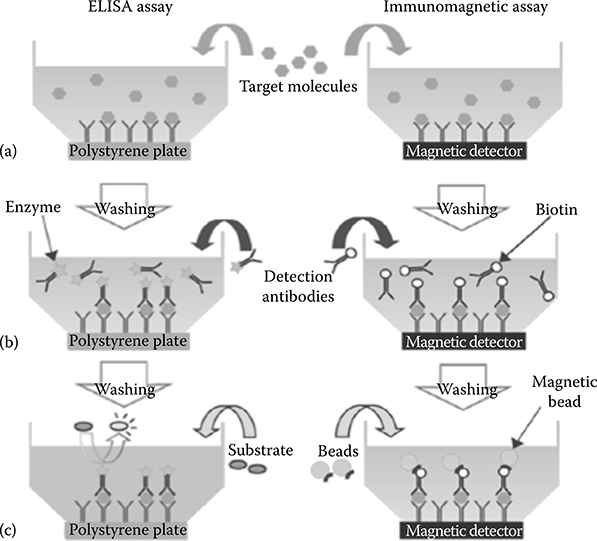
FIGURE 5.1 Comparison of ‘standard’ ELISA (left) to an immunomagnetic assay (right). The procedures are very similar, with major differences being the substrate and label.
The testing device has a substrate that has previously been functionalized with an antibody specific for the compound that needs to be detected (capture antibody). When the sample is introduced (a), molecules of the target bind to the capture antibodies, while other molecules do not. Some of the nontarget molecules might physically adsorb to the substrate, and are removed with a washing step. Finally, a detection antibody is introduced (b), which binds to a different epitope of the target compound. This antibody is usually labeled with an enzyme or a fluorescent marker, commonly known as the reporter label (c). The fluorescence intensity read from the device then provides a proxy for the amount of target compound. ELISA is an example of an affinity-based (because of the use of antibodies for chemical recognition), labeled assay protocol and state-of-art tests using this protocol achieve detection limits below 1 pg/ml.
The main shortcoming of the current test paradigm is the significant delay between sample collection and the processing and notification of the outcome to the end user. For example:
In a disease detection application, patients typically are not notified of the test results before they leave the physician’s facility and return home, a complication that can cause stress and generally decreases compliance. In addition, in applications such as the detection of early biomarkers of cardiac infarction (troponin) or stroke, the delay simply renders the test irrelevant.
In food safety monitoring, this delay translates into shipping delays and ultimately increased cost, as trucks transporting bulk items need to wait for clearance before they can offload their content [1].
In resource-limited or sparsely populated areas, the density of laboratories might be too low to ensure transport of the samples to a central facility in a cost-effective manner before they foul. This is the case in many developing countries, but also in parts of Australia, Russia, and Canada.
Moving the testing site from a central laboratory to the point of need would eliminate the delay and with it the limitations described above. Generally, a point-of-need testing device should not only have high sensitivity (the ability to detect small concentrations of sample) but should also be highly specific to minimize sample preprocessing and purification and hence the need for specialized staff. In addition, it should be inexpensive, small, and have a long shelf life.
Many point-of-need/point-of-care diagnostic devices have been proposed to address this potential market [2]. While these devices employ approaches that differ in both the biochemistry and the physical design, in this chapter we focus on labeled protocols that employ micron- or nanometer-sized super-paramagnetic particles as labels.
Figure 5.1 compares the main steps in a standard ELISA to a similar assay using magnetic beads as labels. With the exception of the different labels, both approaches proceed very similarly. The same antibodies are used in both cases, and the performance of both assays is comparable [3,4]. Magnetic particles can be functionalized with antibodies and have been used in the sciences for over 20 years [5] to purify or separate rare cells out of a population. When employed as labels, they have at least four potential advantages:
Blood has no low-frequency magnetic content, and does not attenuate low-frequency magnetic fields. In contrast, whole blood is optically opaque and presents significant autofluorescence. This fact suggests that magnetic labels have lower intrinsic background than optical labels, and could be used for direct testing in complex matrices such as whole blood. For the same reason, magnetic assays can potentially be performed on samples without prior centrifugation, possibly eliminating a step that is difficult to perform in a point-of-care setting.
Magnetic fields of up to tens of milliteslas can be generated by flowing current through a wire, creating spatially resolved magnetic forces [6]. These forces enable magnetic washing to be substituted for hydrodynamic washing in assays where microfluidic support for the washing step is not available, obviating the extra costs associated with microfluidic systems. Additionally, this magnetic manipulation can be used to speed up assay times by allowing beads to sediment to the surface via magnetic force, which can be much faster than the diffusion used in ELISA and assays with nanosized labels.
Magnetic fields can be measured using a variety of miniaturized magnetic sensors. In contrast, fluorescent labels are usually excited by an LED, and lenses and optical filters are often required to isolate the fluorescent signal and focus it on a detector. This fact suggests that magnetic labels have far greater potential for system miniaturization. In fact, systems employing a single silicon chip for detection have been reported by our group [7,8 and 9], and systems reported by other groups and using two chips and an external magnet have achieved outstanding performance [10].
Unlike enzymatic labels, magnetic beads are inert and have a long shelf life [11].
The rest of this chapter is organized as follows: in Section 5.2, we consider assay protocols, packaging, and sample interface technologies proposed for use with magnetic immunoassays; Section 5.3 focuses on the detection of magnetic labels, with an emphasis on electronic detection through Hall effect devices; and conclusions are drawn in Section 5.4.
5.2 Assay Protocols and Microfluidic and Packaging Technologies for Magnetic Assays Using Micron-Sized Labels
As shown in Figure 5.1 and anticipated in the previous section, assays exploiting magnetic labels (sometimes referred to as magnetic immunoassays or MIA) employ the same basic steps and principles as optical immunoassays. However, there are a few key differences:
The surface on which the capture antibodies are attached (substrate) is typically not a polymer but the surface of the integrated detector, consisting of SiO2 or SiN3.
The electronic detector must be packaged using the sample-manipulation system, while fluid is prevented from reaching the electrical leads.
Magnetic labels often have a diameter of a few microns, as compared to the diameter of tens of nanometers of enzymatic labels or fluorophores.
The impact of these differences on the assay protocol and the surface chemistry is discussed below.
5.2.1 Surface Chemistry for Immobilizing an Antibody
The first step of an immunoassay is to immobilize the capture antibodies on a substrate. For the standard ELISA, a microplate made out of polystyrene is generally used to attach the capture antibodies by physisorption. However, physisorption does not provide a sufficiently stable binding force on silicon or silicon dioxide surfaces to immobilize the capture antibodies. In this case, the biosensor surface must be functionalized using a linker molecule. The most common functional groups for attaching a capture antibody are reactive amine, epoxy, aldehyde, and carboxylic acid. For the amine functional group, 3-aminopropyl triethoxysilane (APTES) is one of the common linkers that has reactive amine groups. The siloxane groups of APTES react with a hydroxyl group on the silicon-based surface by condensation. Then, a glutaraldehyde as bilinker molecule interconnects between APTES and antibodies [12,13]. When the APTES linker is used, the antibodies can be attached on the surface electrostatically. The APTES-modified surface has positive charges that enable interaction with streptavidin (SA). The biotinylated capture antibodies are then added onto the functionalized surface coated with SA at room temperature [4,14,15]. Another common approach is to use a carbodiimide coupling method that uses 1-ethyl-3-(3-dimethylaminopropyl)carbodiimide (EDC) and N-hydroxysuccinimide (NHS) chemicals to generate a carboxylic acid functional group on the capture antibodies.
Alternatively, the overall process to immobilize the capture antibody on the solid substrate can be simplified by using aldehyde silane. By condensation, the aldehyde silane can be functionalized on the silicon-based surface and then allows coupling with amine on the antibodies [16, 17 and 18]. The additional linker protein, such as protein A (PrA), allows control of the direction of the capture antibody. Use of the process described in [19] significantly improved the overall capture efficiency of the target molecule by attaching the Fab binding site of the capture antibody.
Once the surface is functionalized with the capture antibodies, a simple sandwich assay can be started by passivating the overall surface with blocking solution (1% BSA in phosphate buffer saline [PBS]). Various concentrations of target molecules are then loaded onto the activated surface. After a washing step, a detection antibody conjugated with labeling molecules is introduced and incubated to create a full immunocomplex. After the washing step, fluorescence and color intensity can be measured using a microplate reader or a fluorescence microscope.
5.2.2 Microfluidic Integration and Assay Automation
The overall assay process requires various sample mixing, transport, and reaction procedures including multiple sequential steps. To perform these assays effectively, a microfluidic system for reagent delivery, washing, and bead storage can be combined with the integrated sensor. The magnetic bead detector can be placed inside microfluidic systems for automated sample preparation, reagent handling, and washing, facilitating a seamless integration with components. Figure 5.2 shows a magnetic detector chip embedded in a microfluidic system [20]. Since the chip is only a few millimeters high, a printed circuit board is used for assembly.
The normally closed membrane valve that is used in Figure 5.2 provides a high closing force and enables precise manipulation of nano/picoliter sample volumes [21]. However, integration of the microvalve structures often requires the fabrication of via holes to connect the layers [22]. These via holes increase the dead volumes of the device and device complexity.
A lifting gate microfluidic control system enables facile integration with various substrates [23,24]. First, a Hall sensor was mounted on a chip carrier and all the wires were connected using a wire bonding process. Then, the chip carrier was filled with uncured polydimethylsiloxane (PDMS) for interfacing with the lifting gate microfluidic device. Figure 5.3 shows a chip carrier integrated with the microfluidic system containing three bus valves for sample selection and three valves for sample delivery without any via holes. To evaluate the overall functionality, various samples of colored water are pumped through the flow cell on the Hall sensor surface and then clear water is pumped through to demonstrate the washing capability. This technique provides rapid integration of the electronic sensor and automated microfluidic platform. The flex board method (Figure 5.2) [20] can be used for volume manufacturing.

FIGURE 5.2 Immunomagnetic detector chip embedded in a microfluidic system. (Top) The electronic detector chip is flip-assembled onto a printed circuit board (PCB) bonded to the microfluidic device. (Bottom) Photo of the assembled microfluidic device with embedded chip. (From Wu, A., Wang, L., Jensen, E., Mathies, R., and Boser, B., Lab on a Chip, 10, 519–521, 2010.)
5.2.3 Large Label Effects
As discussed earlier, magnetic labels tend to be several orders of magnitude larger than enzymatic labels in optical assays. Label size affects label diffusion behavior, binding behavior, and detectable signal strength; changing the size of the label often requires changes to the entire assay protocol and is difficult to analyze beyond experimental means.

FIGURE 5.3 Lab-on-a-chip platform for biomarker screening that integrated a CMOS Hall sensor with the lifting gate microfluidic system. In the cross-sectional view, the lifting gate device was attached to the chip carrier containing the Hall sensor by manual alignment.
The larger size of labels can be exploited to speed up the dynamics of an assay. Large labels have the advantage of being easily manipulated via electromagnetic or hydrodynamic forces to enable mixing and to accelerate label sedimentation to the sensor surface, resulting in a faster assay protocol and enabling integrated washing [3,4,6]. Table 5.1 shows a comparison between the typical specifications of commercial ELISAs and two published immunoassays utilizing labels approximately a micrometer in diameter. The two large-label assays are on average 20 times faster than ELISA and have comparable detection limits, indicating that microlabels are especially suitable in situations where a fast assay protocol is important.
Table 5.1 Comparison of ELISA to Assays Utilizing Microbeads as Labels
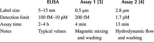
One particular concern with using large labels is increased noise: just 10–100 magnetic labels may constitute a positive signal, whereas in ELISA the label count is in the millions. Intuitively speaking, a result inferred from such a small number of labels may have significant errors caused by binding statistics and label variations. Labels bind to the surface with a Poisson distribution, as shown in [25]. Assay accuracy is typically measured using a coefficient of variation (CV), which is the standard deviation of a signal divided by the mean or the signal when the assay is performed many times under the same conditions. Typical CVs for commercial assay kits are in the range of 5% and better accuracies are rarely required for most immunodiagnostic applications. According to the Poisson distribution, to achieve a CV of 5% or less, at least 400 labels need to bind to the surface and be accounted for. In addition, typical assays require a dynamic range from approximately 100, so an assay area needs to accommodate as many as 40,000 labels on the surface, which translates to about 1 mm2 for 2.8 μm diameter labels (see Figure 5.4). Such areas are over 1000 times larger than those required by optical labels with a 50 nm diameter, but are still practicably achievable on microchips and lab-on-chip systems.

FIGURE 5.4 Minimum detection area for an assay with a dynamic range of 100 utilizing 50 nm and 2.8 μm labels versus the desired CV. When 2.8 μm labels are used, an area over 1000-fold larger is required to suppress biological shot noise.
5.3 Integrated Detection for Magnetic Immunoassays
5.3.1 State-of-the-Art Methods and Limitations
Since the original proposal in [26], several techniques have been proposed for the miniaturized quantification of the number of magnetic labels. In order to understand the challenges of this task, consider the problem of detecting a paramagnetic particle with volume susceptibility X and volume V, situated at a height h directly above a sensor (Figure 5.5).
A magnetic field generator creates a magnetizing field Bmag at the particle location, and a leakage field Bleak at the sensor location. The induced magnetic moment of the particle is . In order to simplify the mathematics, assume the particle is located directly above the sensor so that , and Bmag = 1 mT = Bleak is directed in the z direction. The magnetic field at the sensor evaluates to
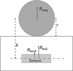
FIGURE 5.5 Generic magnetic bead detection setup.
Last, assume the sensor only responds to magnetic fields directed along z. The magnetic field detected by the sensor is shown in Figure 5.6 as a function of the ratio of height h to particle radius r when the volume permeability of the particle X = 1.
As is apparent from Figure 5.6, the magnetic field from a bead is almost invariably smaller than the leakage field Bleak and as soon as the particle height over the sensor is significantly larger than its radius, this signal also becomes smaller than Earth’s magnetic field.
Care must be taken to position the sensors as close as possible to the particle (reduce h/r), increase its magnetic sensitivity, and isolate the bead response from Earth’s magnetic field through AC excitation. In addition, bead response must be separated from the magnetization field Bmag.

FIGURE 5.6 Typical values for bead signals.
Giant magnetoresistance (GMR) sensors were initially proposed for this purpose in [26,27] and have enjoyed popularity since [28]. They meet all of the guidelines described above. First, as the resistance of a GMR device changes by a few percentage points for each millitesla change in magnetic field, its sensitivity is excellent. In addition, GMR sensors are typically only separated from the sensing surface by a nanometer-thick passivation layer, making h/r close to 1 and effectively maximizing the signal. Last, GMR sensors do not respond to a magnetic field oriented along their hard magnetization axis. The system can then be designed to orient Bmag and Bleak along this hard axis, effectively rejecting the leakage component. In a typical configuration, a GMR device sensitive to the in-plane field and with an out-of-plane (z-directed) hard axis is employed. This has been shown to effectively reduce the leakage field, although it introduces a few issues.
First, the magnetization field must be highly uniform in the sensing area, as small components in the GMR sensitive plane can easily saturate the device. This often dictates the use of physically large, power-hungry, magnetizing coils or permanent magnets. Second, when this technique is used, the sensor response to particles located directly above it is zero, while the maximum occurs for particles off-axis (Figure 5.7) with the sign dependent on the particle location relative to the sensor. Particles located on opposite sides of the sensor induce opposite responses, and their effect is partially canceled.
In addition, fabrication cost and the difficulty of integrating high-performance GMR sensors directly on top of a CMOS are also often cited as disadvantages of this technology. GMR sensors are highly temperature sensitive, and either calibration [10] or analog compensation must be employed. Despite these drawbacks, the highest-sensitivity magnetic immunosensor reported to date utilizes GMR devices for magnetic transduction [29]. GMR sensors using permanent magnets to generate Bmag have also been successfully used to detect magnetic particles transiting over the sensor in a magnetic flow cytometer [30].
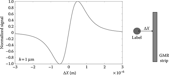
FIGURE 5.7 Normalized GMR sensor response to a 1 μm radius bead as a function of horizontal position. The bias field is in the x direction, while the sensitivity axis is z. Passivation thickness is assumed to be negligible.
Inductive sensors based on planar CMOS coils have also been proposed [31,32]. Current flowing in the coil generates a magnetic field. When a paramagnetic particle is introduced in the magnetic field, energy is stored in the particle by changing the orientation of the magnetic domains, increasing the effective inductance seen at the inductor input port. In [31,32], the inductance change is measured by building an integrated oscillator and measuring the change in its natural frequency with a technique reminiscent of first-generation metal-detector devices. The main advantages of this inductive sensor are its close proximity to the labels (the coil is realized in the top metal layer of a 45 nm CMOS process, so it is separated by roughly 300 nm from the sensing surface) and its low cost. However, this strategy has significant drawbacks. First, the sensing method responds not only to change in inductance but also to change in the loss associated with such inductance (this is indeed the principle of operation of early metal detectors). As a result, the sensor might perform poorly when the solution’s ionic concentration fluctuates. Second, frequency-based detection through an integrated oscillator requires the use of an excitation field with frequency in the GHz range. Many super-paramagnetic labels have dynamics significantly slower than 1 GHz, resulting in reduced response. Third, the inductance change associated with the magnetic particles is very small (100 ppm/particle in [31]) and makes rejecting Bleak in an uncontrolled environment especially challenging.
Last, optical detection of magnetic labels has been proposed in [3,33]. This method has the advantage of a high signal-to-noise ratio when used in combination with large (4.5 μm) labels. The magnetic nature of the labels is in this case primarily used for manipulation, and the potential advantage of detection in whole blood is lost.
Our group [9,34] has primarily focused on magnetic detection using Hall effect sensors, which are also readily available in any CMOS process. The use of Hall effect sensors has similar cost and integration advantages to the use of inductive sensing, but without the sensitivity to loss or the mismatch between magnetization field and particle dynamics that affect the former. There are two crucial challenges when using Hall sensors:
Hall devices are separated from the sensing surface by the entire CMOS metal stack, which can be thicker than 12 μm for a 0.18 μm CMOS process. This results in a h/r ratio of approximately 7 for 4.5 μm particles, giving an extremely small signal of 2 μT.
Since the Hall effect is a manifestation of Lorenz’s force, the sensitivity of Hall sensors is proportional to carrier velocity, and ultimately mobility. In fact, the output of a Hall effect sensor is given by [35]:
The factor GH depends on the sensor geometry and has a maximum value around unity for an approximately square sensor. For μ = 1500 cm2/(V s) and Vbias = 1 V, S = 150 mV/T, between 100 and 1000 times lower than what is achievable by GMR devices.

FIGURE 5.8 Block diagram of Hall effect detection platform.
As shown in the next section, system optimization and circuit design can be used to overcome these challenges and design a magnetic detection platform that, using these sensors, achieves input-referred noise within a factor of 10 of GMR-based systems.
5.3.2 Design of Hall Effect–Based Detectors
Our Hall effect detection platform is comprised of a Hall sensor array, a set of wires generating the magnetizing field Bmag, and readout electronics (Figure 5.8).
The Hall sensor array is 0.6 mm2 and is chosen so that Poisson noise [36] causes the resulting assay results to have a CV of <5% at the detection limit [25], resulting in a minimum number of labels on the array of Nbeads = 400. To sense the highly localized bead field, the sensing area is subdivided into four subarrays of 64 × 40 Hall sensor pixels, for a total of 10,240 sensors.
Column parallel electronics using 160 amplification and digitization chains ensures fast readout.
5.4 Sensor Design and Optimization
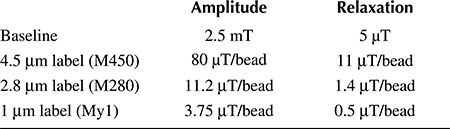
The first step toward the construction of a sensitive detection platform is sensor device optimization. The Hall sensor is realized using the N-well layer of the CMOS process, which offers the highest mobility. The most significant performance improvement is obtained by minimizing the r/h ratio, which can be done by etching through part of the metal stack. The devices described in this chapter use a DRIE step to reduce the distance between the Hall transducer and the sensing surface to 3.2 μm (cross section shown in Figure 5.9), reducing h/r to <2 for 4.5 μm labels, and to 4 for 1 μm labels, and improving the magnetic field Bbead to 80 and 11.2 μT, respectively (Table 5.2).
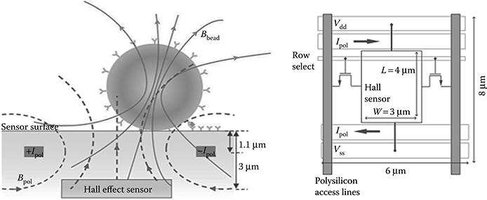
FIGURE 5.9 Cross section and top view of realized sensor pixel.
Table 5.2 Values of Baseline (Bleak) and Signal Bbead for commercial Beads in Different Detection Modes
Since the same integrated circuit generates Bmag and detects Bbead, we further optimize system performance across the generator–detector interface. For a given sensor, when the system is limited by thermal noise, the energy consumed by the detector circuits is proportional to . On the other hand, power consumed by the magnetic field generator is proportional to Bbead. As a result, the magnetizing field should be maximized. In practice, the use of a high magnetic field is limited by saturation effects in the magnetic particles (occurring around Bmag = 20 mT) and by increased thermal effects and layout complexities arising from high current levels [25].
5.5 Magnetization-Based Hall Effect Detection
The most straightforward approach for bead detection is to evaluate the magnetic field at each sensor while the magnetizing field Bmag (and hence the leakage field Bleak) is present (Figure 5.10, left). In the following, we refer to this approach as magnetization detection. For our design, the values of Bmag, Bleak, and Bbead for different labels are reported in the first column of Table 5.2 for magnetization detection for several types of Dynal beads.

FIGURE 5.10 Relaxation measurement (right) compared to magnetization measurement (left) BL indicates the measurement baseline.
It is apparent from the values in Table 5.2 that a high degree of stability is required in the interface gain and offset. Taking as an example the case of 4.5 μm beads, the ratio of Bleak to Bbead is 30. As a result, a 3% change in the cascaded gain or offset of the transducer, electronic interface, and magnetic field generator gives an output as large as the signal from a bead. For the case of 1 μm beads, the ratio of Bleak to Bbead is 800 and the relative stability required is 0.12%. This scenario becomes even worse when the signal from the multiple sensors is averaged to obtain a quantification of the number of beads across the entire sensing array [25,37]. Since at the limit of detection the number of labels is much smaller than the number of Hall sensors being read out, in this case the required stability is enhanced by a factor at least equal to . The above issue can be mitigated by the use of reference sensors that have a nonfunctionalized surface. Due to the third-order dependence of the magnetic field on distance and the sensitivity of Hall effect sensors to stress, matching the reference sensor to the active sensor is only possible to within a few percentage points, making this technique inadequate for detection of particles smaller than 4.5 μm unless calibration is used [34].
5.6 Detectors Based on Magnetic Relaxation
To overcome the stability challenges of magnetization detection, we proposed in [8] to exploit the intrinsic dynamics of magnetization in super-paramagnetic materials to obtain a baseline-free measurement. Figure 5.10 highlights this measurement. The time-dependent magnetization Mdec of a magnetic domain of volume V when an external field B0 is applied for a long time and then suddenly switched off at time t = 0 is given by [38]:
where Km is the material magnetic anisotropy, χ its volume susceptibility, and τ0 ∼ 1 ns. The particles used in this system and in [8] have χ ∼ 1 and τ ∼ 100–300 ns at room temperature. Since it is possible to switch off the on-chip magnetic field generator with a much faster timescale than this τ, we can measure the magnetic field generated by the labels free of any baseline by removing Bmag (and hence Bleak) immediately before connecting the readout electronics to the sensor. As shown in Table 5.2, we obtain an approximately 300-fold reduction in baseline. Because the signal Bbead is now decaying, this comes at the cost of an eightfold reduction in signal strength for commercial particles [37]. The electronic circuit used to perform this measurement is shown in Figure 5.11 together with a timing diagram.
The electronic circuit uses a combination of autozeroing and chopping to suppress the Hall sensor electrical offset, which can be as large as 400 mT, as well as 1/f noise from the electronics.

FIGURE 5.11 Electronics interface schematic and timing diagram.
Only the signal from bead relaxation is converted into a DC current at the output of the V/I converter; this current is then digitized by a first-order incremental A/D converter. The A/D converter samples the signal current inside the loop, resulting in boxcar sampling [39] and further noise reduction. A nested chopper loop with digital demodulation eliminates the input offset due to the A/D converter (up to 500 μT). The up-conversion mechanism of this chopper is implemented, modulating the phase of the magnetization field (Figure 5.11). Each readout chain spans the width of two columns of the Hall sensor array. Electronics are therefore placed at the top and bottom periphery of the array to ensure that one readout serves each column without complex routing. Each chain consumes 330 μW from a 2 V supply to achieve an input-referred noise of 10.8 nV/rt(Hz), or (once referred to the Hall sensor input) 216 nV/rt(Hz). By comparison, the GMR-based detection system in [40] achieves an input-referred noise of 50 nT/rt(Hz) while using sensors that are >50-fold more sensitive. The total power consumption of the readout is 66 mW with all 160 channels active. An additional 128 mW is consumed by the magnetization field generator. Finally, the Hall sensor array consumes 352 mW, bringing the total power consumption to 546 mW. Since the system needs approximately 8 s to measure the number of 2.8 μm beads present on its surface, the energy cost of the detection operation is only 4 J.
The whole system is integrated in a 3.5 mm × 5.1 mm × 0.18 μm CMOS chip (Figure 5.12) and has on average a baseline of only 7 μT, a reduction of >300-fold compared to the magnetizing field of 2.5 mT.
Figure 5.13 shows the measured response of this interface as a function of the number of beads present on the sensor surface (optical count). Extrapolated noise floors range from 8 beads (for M450) to 200 beads (for 1 μm My1 beads) and are comparable with the noise floor from biological shot noise [37].
The ultimate ability of the system to detect field from small particles is evaluated through Allan deviation, which is shown in Figure 5.14 as a function of time for both magnetization and relaxation detection methods. The minimum Allan deviation for relaxation measurements is 9 nT and occurs at a measurement time of approximately 30 min, while the equivalent figures for magnetization are 120 nT and 30 s.
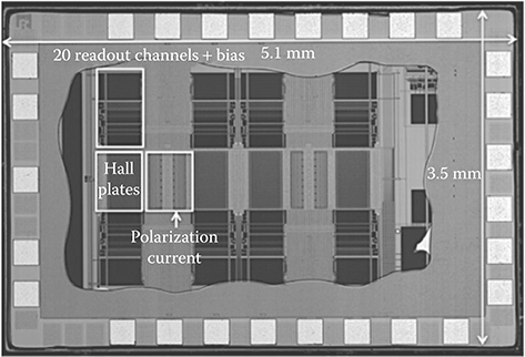
FIGURE 5.12 Detector chip photograph.
This limit is difficult to reach in practice as it only applies to temperature-stable laboratory conditions. As a result, the reduced baseline of the relaxation measurement is even more attractive as it also translates to simpler calibration and lower temperature sensitivity. In Figure 5.15 and in [8], we showed that the temperature sensitivity of this platform is approximately one 2.8 μm bead for a 1°C temperature increase in magnetization. For relaxation measurements, this figure is decreased approximately 40-fold.
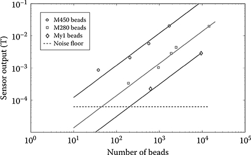
FIGURE 5.13 Digitized sensor output as a function of number of labels.

FIGURE 5.14 Allan deviation in relaxation and magnetization measurements.
5.7 Conclusions and Future Outlook
Magnetic immunoassays could have substantial advantages compared to optical methods, giving the possibility to drastically reduce sample processing, combine separation and detection, and enable system miniaturization through nonoptical detection. In this chapter, we reviewed several research-grade detector technologies that are currently available, focusing on the low-cost Hall effect–based technology developed in our group.
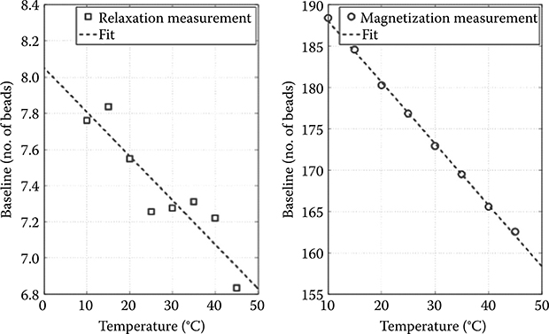
FIGURE 5.15 Temperature dependence of baseline for relaxation (left) and magnetization (right) measurements.
Further work is however required in a number of areas in order to make magnetic immunoassays practical. On the biochemistry side, there is still significant resistance toward the idea that micron-sized magnetic beads, when bound to nanometer-sized antibodies, do not alter their binding kinetics, degrading assay sensitivity or selectivity. Further research is required to either disprove or confirm this hypothesis. Demonstration of integrated detection with separation in a complex matrix is also still lacking, although progress in this direction has been achieved using electrochemical detection methods.
In the meantime, excellent results have been obtained by [28] using 50 nm nanoparticles as tags. Due to their small size, these labels are expected to have much less significant interaction with the antibody binding kinetics and are hence more likely to be accepted by the assay community as labels. The task of detecting such small particles in a completely integrated fashion is however far from accomplished. Fortunately, single-nanoparticle detection is not necessary. For example, in [10] a GMR-based integrated interface is reported that is capable of detecting 5000 nanoparticles while achieving a biological limit of detection of 10 fM. An external magnet is still required to generate a uniform magnetizing field.
Hall effect detection of nanometer-sized particles has not been reported. However, a calculation shows that the magnetization field from an aggregate of 5000 nanoparticles, in the system described in [37], is 7.2 μT. If the relaxation behavior of these particles were the same as that of Dynal beads, the average relaxation field would be 0.9 μT, well within the detection range of the system. Experiments with nanoparticles failed however to confirm this hypothesis, likely due to a different relaxation behavior. As a result, while the development of a Hall effect–based detector capable of sensing minute concentrations of nanoparticles is an open research problem, it is likely achievable with current technology.
The Hall effect sensing could also be potentially improved through technology scaling. For example, a metal-stack height of 90 nm is approximately half of that of 180 nm, giving an eightfold improvement in field strength for small particles. In practice, the improvement is less than eightfold because the thinner metals and lower supply voltage also require larger on-chip current-carrying wires and hence a larger pixel size, ultimately reducing the magnetizing field [25]. To date, no Hall effect bead detector has been realized in technologies with feature size smaller than 180 nm, making this a natural next goal for research.
References
1. Palchetti, I. and M. Mascini. Electroanalytical biosensors and their potential for food pathogen and toxin detection. Analytical and Bioanalytical Chemistry 391(2): 455–471 (2008).
2. Myers, F. B. and L. P. Lee. Innovations in optical microfluidic technologies for point-of-care diagnostics. Lab on a Chip 8(12): 2015–2031 (2008).
3. Bruls, D. M., T. H. Evers, J. A. H. Kahlman, P. J. W. van Lankvelt, M. Ovsyanko, E. G. M. Pelssers, J. J. H. B. Schleipen, et al. Rapid integrated biosensor for multiplexed immunoassays based on actuated magnetic nanoparticles. Lab on a Chip 9(24): 3504–3510 (2009).
4. Kim, J., E. Jensen, M. Megens, B. E. Boser, and R. Mathies. Integrated microfluidic processor for solid phase capture immunoassays. Lab on a Chip 11(18): 3106–3112 (2011).
5. Miltenyi, S., W. Müller, W. Weichel, and A. Radbruch. High gradient magnetic cell separation with MACS. Cytometry 11(2): 231–238 (1990).
6. Florescu, O., K. Wang, P. Au, J. Tang, E. Harris, P. R. Beatty, and B. E. Boser. On-chip magnetic separation of superparamagnetic beads for integrated molecular analysis. Journal of Applied Physics 107(5): 054702 (2010).
7. Gambini, S., K. Skucha, P. Liu, J. Kim, R. Krigel, R. Mathies, and B. E. Boser. A CMOS 10 kPixel baseline-free magnetic bead detector with column-parallel readout for miniaturized immunoassays. In Proceedings of the 2012 IEEE International Solid-State Circuits Conference Digest of Technical Papers (ISSCC), pp. 126–128. 19–23 February 2012, IEEE, San Francisco, CA.
8. Liu, P., K. Skucha, M. Megens, and B. Boser. A CMOS Hall-effect sensor for the characterization and detection of magnetic nanoparticles for biomedical applications. IEEE Transactions on Magnetics 47(10): 3449–3451 (2011).
9. Aytur, T., J. Foley, M. Anwar, B. Boser, E. Harris, and P. R. Beatty. A novel magnetic bead bioassay platform using a microchip-based sensor for infectious disease diagnosis. Journal of Immunological Methods 314(1): 21–29 (2006).
10. Gaster, R. S., D. A. Hall, C. H. Nielsen, S. J. Osterfeld, H. Yu, K. E. Mach, R. J. Wilson, et al. Matrix-insensitive protein assays push the limits of biosensors in medicine. Nature Medicine 15(11): 1327–1332 (2009).
11. Lee, H., D. Ham, and R. M. Westervelt. CMOS Biotechnology. Springer, New York (2007).
12. Diao, J., D. Ren, J. R. Engstrom, and K. H. Lee. A surface modification strategy on silicon nitride for developing biosensors. Analytical Biochemistry 343(2): 322–328 (2005).
13. Ouyang, H., L. A. DeLouise, B. L. Miller, and P. M. Fauchet. Label-free quantitative detection of protein using macroporous silicon photonic bandgap biosensors. Analytical Chemistry 79(4): 1502–1506 (2007).
14. Sivagnanam, V., B. Song, C. Vandevyver, and M. A. M. Gijs. On-chip immunoassay using electrostatic assembly of streptavidin-coated bead micropatterns. Analytical Chemistry 81(15): 6509–6515 (2009).
15. Sivagnanam, V., A. Sayah, C. Vandevyver, and M.A.M. Gijs. Micropatterning of protein-functionalized magnetic beads on glass using electrostatic self-assembly. Sensors and Actuators B: Chemical 132(2): 361–367 (2008).
16. Choi, S. H., J. W. Lee, and S. J. Sim. Enhanced performance of a surface plasmon resonance immunosensor for detecting Ab-GAD antibody based on the modified self-assembled monolayers. Biosensors and Bioelectronics 21(2): 378–383 (2005).
17. Kumeria, T., M. D. Kurkuri, K. R. Diener, L. Parkinson, and D. Losic. Label-free reflectometric interference microchip biosensor based on nanoporous alumina for detection of circulating tumour cells. Biosensors and Bioelectronics 35(1): 167–173 (2012).
18. Kim, J., J. Elsnab, C. Gehrke, J. Li, and B. K. Gale. Microfluidic integrated multi-walled carbon nanotube (MWCNT) sensor for electrochemical nucleic acid concentration measurement. Sensors and Actuators B: Chemical 185: 370–376 (2013).
19. Yuan, Y., H. He, and L. J. Lee. Protein A-based antibody immobilization onto polymeric microdevices for enhanced sensitivity of enzyme-linked immunosorbent assay. Biotechnology and Bioengineering 102(3): 891–901 (2009).
20. Wu, A., L. Wang, E. Jensen, R. Mathies, and B. Boser. Modular integration of electronics and microfluidic systems using flexible printed circuit boards. Lab on a Chip 10(4): 519–521 (2010).
21. Grover, W. H., A. M. Skelley, C. N. Liu, E. T. Lagally, and R. A. Mathies. Monolithic membrane valves and diaphragm pumps for practical large-scale integration into glass microfluidic devices. Sensors and Actuators B: Chemical 89(3): 315–323 (2003).
22. Skelley, A. M., J. R. Scherer, A. D. Aubrey, W. H. Grover, R. H. Ivester, P. Ehrenfreund, F. J. Grunthaner, J. L. Bada, and R. A. Mathies. Development and evaluation of a micro-device for amino acid biomarker detection and analysis on Mars. Proceedings of the National Academy of Sciences of the United States of America 102(4): 1041–1046 (2005).
23. Kim, J., M. Kang, E. C. Jensen, and R. A. Mathies. Lifting gate polydimethylsiloxane microvalves and pumps for microfluidic control. Analytical Chemistry 84(4): 2067–2071 (2012).
24. Kim, J., E. C. Jensen, A. M. Stockton, and R. A. Mathies. Universal microfluidic automaton for autonomous sample processing: Application to the Mars organic analyzer. Analytical Chemistry 85(16): 7682–7688 (2013).
25. Skucha, K., S. Gambini, P. Liu, M. Megens, J. Kim, and B. E. Boser. Design considerations for CMOS-integrated Hall-effect magnetic bead detector for biosensor applications. IEEE Journal of Microelectromechanical Systems 22(6): 1327–1338 (2013).
26. Edelstein, R. L., C. R. Tamanaha, P. E. Sheehan, M. M. Miller, D. R. Baselt, L. J. Whitman, and R. J. Colton. The BARC biosensor applied to the detection of biological warfare agents. Biosensors and Bioelectronics 14(10): 805–813 (2000).
27. Megens, M. and M. Prins. Magnetic biochips: A new option for sensitive diagnostics. Journal of Magnetism and Magnetic Materials 293(1): 702–708 (2005).
28. Osterfeld, S. J., H. Yu, R. S. Gaster, S. Caramuta, L. Xu, S.-J. Han, D. A. Hall, et al. Multiplex protein assays based on real-time magnetic nanotag sensing. Proceedings of the National Academy of Sciences of the United States of America 105(52): 20637–20640 (2008).
29. Gaster, R. S., D. A. Hall, and S. X. Wang. nanoLAB: An ultraportable, handheld diagnostic laboratory for global health. Lab on a Chip 11(5): 950–956 (2011).
30. Helou, M., M. Reisbeck, S. F. Tedde, L. Richter, L. Bär, J. J. Bosch, R. H. Stauber, E. Quandt, and O. Hayden. Time-of-flight magnetic flow cytometry in whole blood with integrated sample preparation. Lab on a Chip 13(6): 1035–1038 (2013).
31. Wang, H., Y. Chen, A. Hassibi, A. Scherer, and A. Hajimiri. A frequency-shift CMOS magnetic biosensor array with single-bead sensitivity and no external magnet. In Proceedings of the IEEE International Solid-State Circuits Conference-Digest of Technical Papers, ISSCC, pp. 438–439. 8–12 February 2009, IEEE, San Francisco, CA.
32. Wang, H., C. Sideris, and A. Hajimiri. A frequency-shift based CMOS magnetic biosensor with spatially uniform sensor transducer gain. In Proceedings of the IEEE Custom Integrated Circuits Conference (CICC), pp. 1–4. 19–22 September 2010, IEEE, San Jose, CA.
33. Lehmann, U., M. Sergio, S. Pietrocola, E. Dupont, C. Niclass, M. A. M. Gijs, and E. Charbon. Microparticle photometry in a CMOS microsystem combining magnetic actuation and in situ optical detection. Sensors and Actuators B: Chemical 132(2): 411–417 (2008).
34. Florescu, O., M. Mattmann, and B. E. Boser. Fully integrated detection of single magnetic beads in complementary metal-oxide-semiconductor. Journal of Applied Physics 103(4): 046101–046101-3 (2008).
35. Popović, R. S. Hall Effect Devices. Taylor & Francis, Abingdon, UK (2004).
36. Hassibi, A., S. Zahedi, R. Navid, R. W. Dutton, and T. H. Lee. Biological shot-noise and quantum-limited signal-to-noise ratio in affinity-based biosensors. Journal of Applied Physics 97(8): 084701 (2005).
37. Gambini, S., K. Skucha, P. P. Liu, J. Kim, and R. Krigel. A 10 kPixel CMOS Hall sensor array with baseline suppression and parallel readout for immunoassays. IEEE Journal of Solid-State Circuits 48(1): 302–317 (2013).
38. Fannin, P. C. and S. W. Charles. On the calculation of the Neel relaxation time in uniaxial single-domain ferromagnetic particles. Journal of Physics D, Applied Physics 27(2): 185–188 (1994).
39. Van de Plassche, R. J. CMOS Integrated Analog-to-Digital and Digital-to-Analog Converters, vol. 2. Kluwer Academic Publishers, Dordrecht (2003).
40. Hall, D. A., R. S. Gaster, K. A. A. Makinwa, S. X. Wang, and B. Murmann. A 256 pixel magnetoresistive biosensor microarray in 0.18 µm CMOS. IEEE Journal of Solid-State Circuits 48(5): 1290–1301 (2013).