
Chapter 5. Introduction to Microwave Active Devices
Chapter Outline
5.2 Field Effect Transistor (FET)
5.3 Bipolar Junction Transistor (BJT)
5.5 Extraction of Equivalent Circuits
5.1 Introduction
Before 1970, available microwave semiconductor devices were largely diodes and Si BJTs (bipolar junction transistors). Gunn, IMPATT, varactor, PIN, and Schottky diodes were frequently used in microwave applications. A reverse-biased pn junction diode has a depletion capacitance that changes when the reverse-biased DC voltage changes. A varactor diode is a variable capacitor that utilizes this depletion capacitance property. The varactor diode is often used to adjust the oscillation frequency and it can also amplify a weak signal. A parametric amplifier employs the varactor diode and its operation resembles that of a mixer. In the past, the parametric amplifier played an important role as a low-noise amplifier because there were no suitable active devices for amplifier applications, especially for low-noise amplifiers. Another diode using the pn junction is the PIN diode. By creating an intrinsic-region (I-region) in the pn junction, the PIN diode can be formed, and the resistance of this I-region depends on the DC voltage. Based on this property, electronic switches can be implemented in the microwave region. In addition, by combining the PIN diodes with transmission lines of the appropriate length, they can also be utilized as digital phase shifters. A PIN diode can also function as an analog-type variable attenuator.
A Schottky diode has, for a long time, been used in detectors and mixers due to its rectifying property. The Schottky diode uses majority carrier diffusion while the pn diode uses minority carrier diffusion. Consequently, the Schottky diode has no diffusion capacitance that is associated with minority carriers. Thus, the Schottky diode provides a number of benefits when used in mixers at high frequencies.
Until the 1970s, Gunn diodes and IMPATT diodes were primarily used as active components in oscillators and amplifiers. In those days, it was difficult to utilize transistors at frequencies higher than 4 GHz. The DC characteristics of these diodes showed a negative resistance when they were biased appropriately. By using negative resistance, it was much easier to design oscillators and they could also be used as amplifiers. Since the reflection coefficient of devices with a negative resistance is greater than 1, the Gunn and IMPATT diodes could be configured as reflection amplifiers in combination with a circulator. However, one problem with these diodes was that they were not very efficient. As a result, heat dissipation always had to be considered. Therefore, they were used in the construction of circuits with waveguides that easily adapted to thermal design. These heat problems become important limiting factors in circuit integration. Another disadvantage was that these diodes could not be integrated with other devices in a single process, making it intrinsically difficult to build up complex-functioning integrated circuits that need other devices such as Schottky or varactor diodes used for mixer or frequency control.
Based on their operation, transistors can be generally categorized into two types: the bipolar junction transistor (BJT) and the field effect transistor (FET). BJTs use two carriers, holes and electrons, and they use a diffusion mechanism in current flow. BJTs control current flow by raising or lowering the barrier height formed at junctions. The number of diffusing carriers depends on the barrier height, which is altered by the voltage across the base-emitter junction. In contrast, FETs use one majority carrier, an electron, and they use a drift mechanism in current flow. An FET forms a channel through which electrons can flow. The number of electrons flowing through the channel can be controlled by narrowing or widening the channel’s thickness, which is achieved by controlling the gate voltage. FETs are also classified according to their channel formation. There are two kinds of channel formation: enhancement type and depletion type. In the enhancement type, the channel is not formed under the gate when the applied gate voltage is below a threshold voltage. The channel under the gate is formed by applying the adequate gate voltage. The gate voltage collects the carriers with opposite polarity and the accumulated carriers under the gate form the channel. In contrast, in the depletion type, the channel with carriers is formed in advance and the gate voltage is used to deplete the channel by repelling the carriers in the channel with the same polarity. Thus, the gate voltage is used to control the channel conductivity in both types of FETs.
The silicon process was the only available process technology for the fabrication of transistors until the 1970s. Microwave Si BJTs, which improved low-frequency BJTs in many ways, were exclusively used up to the range of microwave frequencies. However, these Si BJTs were not suitable for applications at frequencies higher than 4 GHz. In the early 1970s, the GaAs (gallium arsenide) MESFET (MEtal Semiconductor FET) or simply GaAs FET was developed as a result of the advance of the GaAs compound semiconductor process technology. The electron mobility in the GaAs is six times faster than in the Si. With this electron mobility advantage, GaAs FET has far better performance than the Si transistor. When GaAs FETs are fabricated using similar technology to the Si process, their performance is also as much as six times better. With the emergence of GaAs FETs, Gunn diodes, which had been popular until that time, became obsolete for amplifiers and oscillators in microwave frequencies up to the Ku band, and their application is now limited to the millimeter-wave frequencies. However, a further improvement in the characteristics of GaAs FETs led to the emergence of the HEMT (high-electron-mobility transistor) and the pHEMT (pseudomorphic HEMT). It is now possible to construct an integrated circuit up to a frequency of 200 GHz with these HEMTs. Thus, the future use of Gunn or IMPATT diodes in the millimeter wave remains unclear.
Three-terminal devices such as BJTs and GaAs MESFETs have several advantages when compared to diodes. They provide a flexibility in circuit design that can be applied to various components such as amplifiers, oscillators, and so on. In terms of efficiency, they are superior to the Gunn or other diodes. They do not require heat dissipation structures if they are not operated at significantly high power. They can also be used as switches by controlling the gate or base voltage. In addition, the characteristics of the varactor diode are inherently included in these devices, and they can be utilized in planar circuits as well, making them superior to other active components in terms of their advantages for integration. Every year, the high-frequency characteristics and performance of BJTs and GaAs MESFETs have been steadily improved by many researchers and even to date, their performance has been improved every year by applying new materials or new operating principles.
In this chapter, we will briefly investigate the operation and characteristics of these transistors used in microwave applications. Among diodes, we will also look at the varactor diode in oscillator design. The varactor diode is discussed further in Chapter 10. The operating principles and performance of Schottky diodes will also be discussed in the mixer design found in Chapter 12.
5.2 Field Effect Transistor (FET)
As explained in this chapter’s introduction, there are two major types of three-terminal semiconductor devices: FETs and BJTs. The MOSFET (metal-oxide semiconductor FET), based on the silicon process, is the most widely used three-terminal device for implementing low-frequency integrated circuits, including digital circuits. However, during the 1970s, the performance of the MOSFETs fabricated with the Si process were not adequate for microwave applications, and their high-frequency performance was inferior to that of BJTs fabricated with the Si process. The GaAs MESFET (metal semiconductor FET) fabricated using the GaAs compound semiconductor technology was the first type of FET device applied to microwave circuits. Since the electron mobility in the GaAs is about six times faster than the Si, it was possible to fabricate an FET-type device using concurrent semiconductor process technologies.
The performance of GaAs MESFETs has been further improved with recent advances in process technologies that have made the fabrication of complicated epi-layer structures possible. As a result, GaAs pHEMTs can now be used at frequencies reaching several hundred GHz. In addition, the Si complementary MOS (CMOS) fabrication technology has demonstrated remarkable advances in various mobile-communication services. Recently, many CMOS circuits operating at millimeter wave frequencies have been reported. However, the basic operation of CMOS circuits is the same as it was in the past, a subject that is extensively covered in many textbooks related to electronic circuits. Thus, in this section, we will consider the operation and equivalent circuits of FETs based on GaAs MESFETs among the many other types of FETs.
5.2.1 GaAs MESFET
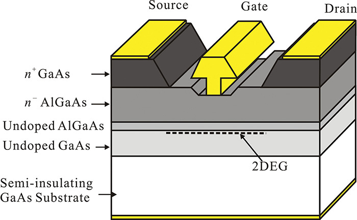
A top planar view of a GaAs FET with a gate length of 0.3 μm and a gate width of 250 μm is shown in Figure 5.1. The cross-section at A-A’ in that figure is also shown in Figure 5.2. In the GaAs FET shown in Figure 5.2, an electron-rich n-type epitaxial layer (epi-layer) is grown on the semi-insulating GaAs substrate. On the epitaxial layer, two ohmic contacts are formed for the drain and source terminals, while a Schottky contact is formed for the gate terminal. The Schottky diode formed between the gate and the epitaxial layer is reverse-biased, applying a negative gate voltage, and no gate current flows. However, a depletion region with no carriers occurs in the epitaxial layer due to the reverse-biasing gate voltage. The further increase of the negative gate voltage widens the depletion region and makes the channel narrow. This causes the drain-source current to decrease. Therefore, the drain-source current can be controlled using the gate voltage.
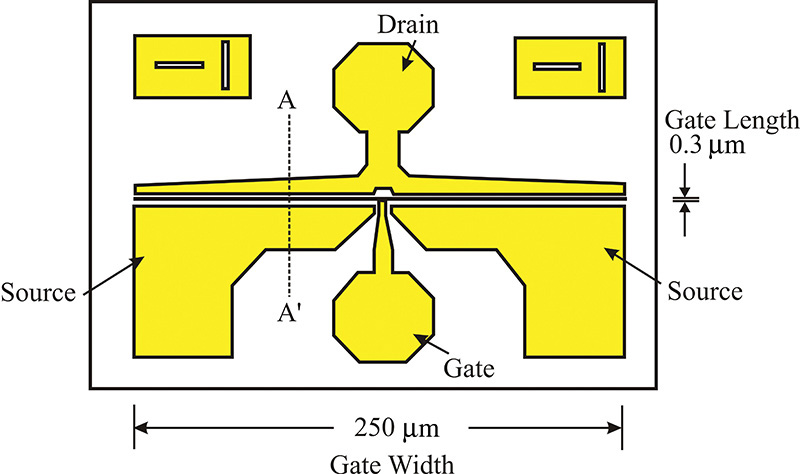
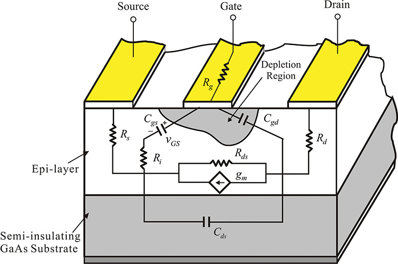
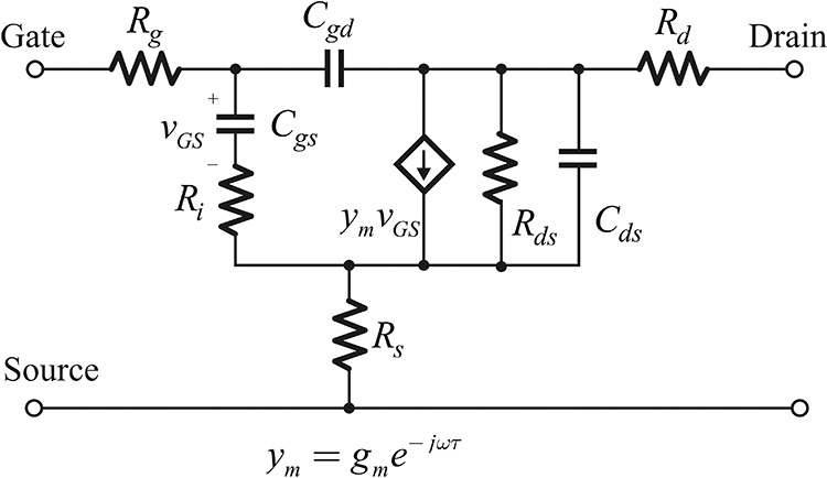
Figure 5.2 Cross-section of a GaAs FET and its equivalent circuit. Cgs and Cgd represent the depletion capacitances of the Schottky diode. The transconductance gm represents the current controlled by the voltage across Cgs. Rd and Rs come from the ohmic contact resistances. Rg comes from the gate metallization resistance. Rds and Cds represent the resistance and capacitance between the drain and source terminals.
The equivalent circuit of a GaAs FET is shown in Figure 5.2. Resistors Rs and Rd represent the ohmic resistances that occur from the source and drain ohmic contacts. Resistor Rg represents the gate metallization resistance deposited to form the Schottky diode. The dependence of the drain current on the gate voltage is represented by the transconductance gm, and that of the drain current on vDS is represented by the resistance Rds. In contrast with the Rg, Rs, and Rd shown in the figure, gm and Rds are nonlinear components and they represent the FET’s DC characteristics. Resistor Ri is called channel resistance and represents the resistance between the depletion region and source terminals. The depletion region that occurs in the gate region is not directly connected to the source terminal but is connected to the source through a channel region. Ri represents the resistance of such a channel resistance to the source terminal.
Capacitors Cgs and Cgd represent the capacitances caused by the depletion region between the gate and the source, and between the gate and the drain terminals. The DC-bias dependence of these capacitors has characteristics similar to those of a depletion capacitance. On the other hand, Cds represents the capacitance occurring between the terminals of the source drain. Capacitor Cds between the drain and source terminals results from the capacitances through the channel and air regions. Capacitor Cds is also considered to be nonlinear and its characteristics are different from those of the depletion capacitance. The equivalent circuit in Figure 5.2 is redrawn in Figure 5.3. The transconductance is expressed as ym = gme–jωτ because the drain current flows with a time delay of τ compared to the gate-source control voltage.
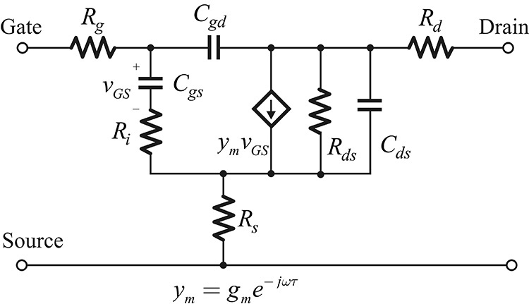
Figure 5.3 Small-signal GaAs MESFET equivalent circuit redrawn from Figure 5.2. Here, τ represents delay because the drain current is not instantly controlled by the gate-source voltage.
5.2.2 Large-Signal Equivalent Circuit
Figure 5.4 shows a large-signal equivalent circuit for a GaAs FET. Since the physical origin of Rg, Rs, and Rd is itself linear, these circuit elements can be treated as linear components. The physical operations of the gate-source and the gate-drain junctions are originated from Schottky diodes, and iGD and iGS can be described by the Schottky diode I–V characteristics shown in Equations (5.1) and (5.2).
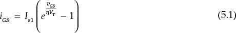
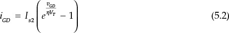
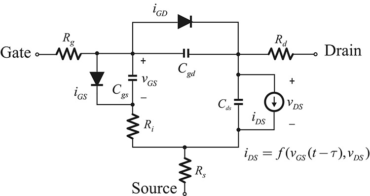
Figure 5.4 Large-signal equivalent circuit of a GaAs MESFET: iGD and iGS represent the Schottky diode formed between the gate drain and the gate source, respectively. Cgs and Cgd are depletion capacitances of the Schottky diode. The current source iDS represents the current source, depending on the gate-source and drain-source voltages. Other circuit elements are assumed to be linear elements.
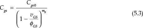
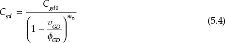
By measuring the forward DC current characteristics of the Schottky diode, the parameters such as ideality factor η and saturation current Is can be determined. Also, since Cgs and Cgd originate from the depletion capacitance, they can be determined by measuring the C–V characteristics given by Equations (5.3) and (5.4).
In contrast, the nonlinear characteristics of Cds and Ri are not so significant, and the small-signal values of Cds and Ri can be used in the large-signal model.
However, the IDS–VDS characteristics of the GaAs FET are significantly different from those of the low-frequency FET devices. Therefore, a new mathematical model is required to represent its IDS–VDS characteristics, which are shown in Figure 5.5. There can be various mathematical models representing the IDS–VDS characteristics, but of these, there are three that are well known.
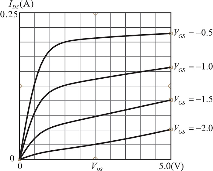
The Curtice model describes the characteristics shown in Figure 5.5 using the equation (1 + λVDS)tanh(αVDS). The function tanh(x) can be approximated by x for small x, and approaches 1 as x → ± ∞. Thus, for a small VDS, (1 + λVDS)tanh(αVDS) behaves as a straight line for VDS because (1 + λVDS)tanh(αVDS) ≅ αVDS, which steeply increases for VDS. In contrast, for a sufficiently large VDS, the equation can be approximated as (1 + λVDS), which increases slightly for VDS. Thus, the IDS–VDS curves can be qualitatively represented by (1 + λVDS)tanh(αVDS). Now, we can determine the given equation through curve fitting of the measured IDS–VDS characteristics with constants α and λ.
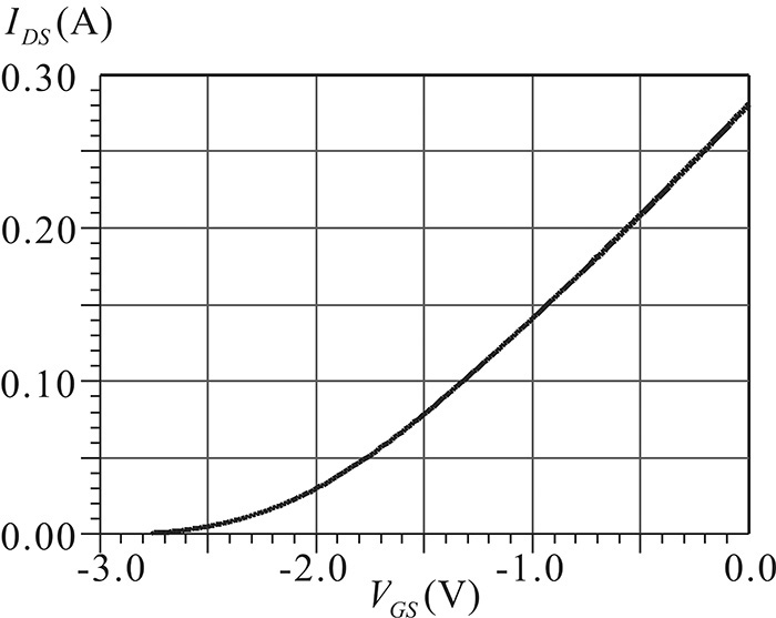
However, since the dependence of the drain current on VGS is close to the parabola shown in Figure 5.6, the IDS–VGS characteristics can be modeled using a quadratic equation. In reality, the use of the quadratic equation does not closely approximate the measured results. The cubic equation given in Equation (5.5) may be a better way to describe the IDS–VGS characteristics in Figure 5.6 because this equation has three degrees of freedom. In addition, the IDS–VGS characteristics depend to some degree on VDS. In order to describe this, V1 is used instead of VGS, which depends linearly on VDS as in Equation (5.5b). Thus, the IDS–VDS characteristics shown in Figure 5.5 are expressed mathematically in Equations (5.5a) and (5.5b).
For the Materka model, the relationship between the drain current and VGS is described in a well-known parabolic relationship, and the slope for VDS is expressed by modifying tanhx in the IDS–VDS characteristics as shown in Equations (5.6a) and (5.6b).
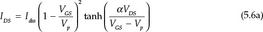
Note that the pinch-off voltage Vp also depends linearly on VDS.
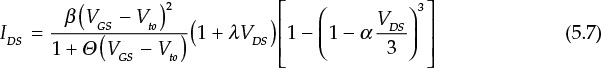
The Raytheon model is a mathematical model developed by the Raytheon Corporation and is expressed in Equation (5.7).
In addition, there are various other mathematical models that are difficult to distinguish in terms of their pros and cons, but they all describe the DC drain-current dependences on VGS and VDS, and all of them can be used in performing large-signal simulations. In addition, it is worth noting that all the equations from (5.5) to (5.7) represent a mathematical relationship for DC characteristics. Since the RF drain-current iDS depends on RF gate voltage vGS with a time delay of τ, the large-signal microwave operations of iDS can be modeled by replacing VGS by vGS(t-τ) in the equations from (5.5) to (5.7) using Equation (5.8):
This equation can be used as a mathematical model for microwave operation.
5.2.3 Simplified Small-Signal Equivalent Circuit and S-Parameters
The equivalent circuit shown in Figure 5.3 clearly explains the device’s physical origin, but it is rather complicated. Resistors Rg, Rs, and Rd are the resistances that occur due to the contacts, and the values of the elements are generally small. Also, these resistors are not regarded as intrinsic parts of FETs, and so they are called extrinsic elements. Thus, their values are usually approximated to zero, and the approximate, simplified, small-signal equivalent circuit that results is shown in Figure 5.7. This simplified equivalent circuit is used to explain qualitatively the measured S-parameters of the GaAs FET.
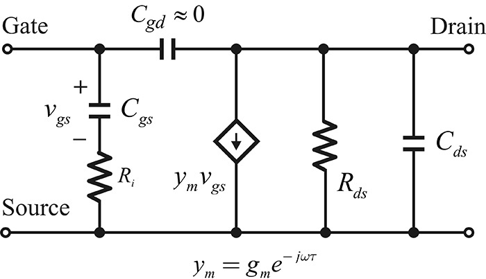
Figure 5.7 A simplified equivalent circuit of an FET. The extrinsic circuit elements Rg, Rd, and Rs shown in Figure 5.3’s equivalent circuit are omitted here.
For increased simplification, further approximation is possible because the depletion capacitance Cgd is generally small compared to Cgs and sometimes it is also assumed to be 0. Thus, the FET’s input and output are isolated. Such an approximation is called a unilateral approximation.
Figure 5.8 shows the measured S-parameters of a typical chip-state GaAs FET. After the GaAs FET chip was assembled by wire bonding on the carrier, as shown in Figures 5.9(b) and 5.9(c), the carrier assembly was mounted on a jig, as shown in Figure 5.9(a). In Figure 5.9(b), the reference planes are shown. Thus, the measured S-parameters usually include the inductance of bonding wires.
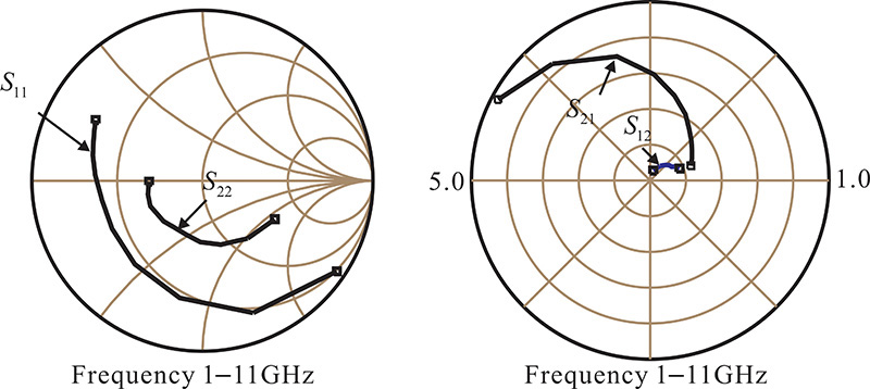
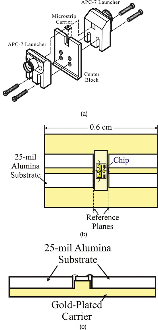
Figure 5.9 Illustration of the assembly for S-parameter measurement of a GaAs FET: (a) assembly of the test jig, (b) top view of the microstrip carrier, and (c) cross-sectional view of the microstrip carrier1
1. Agilent Technologies, High-Frequency Transistor Primer Part IV, GaAs FET Characteristics, 1999. Available at http://paginas.fe.up.pt/~hmiranda/etele/trans_primer4.pdf.
In Figure 5.8, S11 and S22 are related to input and output impedances. Thus, they are usually plotted on the Smith chart, as shown on the left side of Figure 5.8. In contrast, S12 and S21 are the transfer functions and so they are plotted on the polar chart on the right side of Figure 5.8 to show their magnitude and phase. On the polar chart, the radius is set to 5.0 for S21 and the radial division scale is found to be 1.0. However, as S12 is small, the radius is set to 1.0 and the radial division scale becomes 0.2. The frequency responses of the S-parameters can be explained using the simplified equivalent circuit shown in Figure 5.7.
From Figure 5.9, the measured S11 includes the bonding-wire inductance. The input impedance of the FET is then found to be a series R-L-C circuit approximating Cgd = 0 in the simplified equivalent circuit. For a frequency change, the reactance of L and C changes but Ri is constant. Thus, the locus of S11 lies in a constant resistance circle for a frequency change. At low frequency, the circuit behaves like a series R-C circuit. However, as the frequency increases, the inductance of the bonding wire becomes dominant, and so the circuit behaves as a series R-L circuit. From this, the resistance at the series resonance corresponds to the channel resistance Ri in the simplified equivalent circuit, but if the ignored contact resistance were to be considered, it would approximate the value of Ri + Rg + Rs. In addition, applying the method explained in Example 2.2 of Chapter 2, the bonding-wire inductance and capacitance can be obtained by calculating the L and C values at resonance. The resulting capacitance and inductance correspond approximately to Cgs and the bonding-wire inductance.
In the case of S22, the drain-source impedance can be approximated by a circuit of Rds and Cds connected in parallel. Therefore, as the frequency approaches 0, the drain-source impedance approaches Rds. As the frequency increases, S22 moves along a constant conductance circle and the trajectory appears in the capacitive region due to capacitor Cds. As the frequency further increases, S22 is observed to move away from the constant conductance circle and to approximate a constant resistance circle similar to S11 due to the effects of bonding-wire inductor and Cgd.
In the case of S21, at an extremely low frequency, S21 can be computed as
Using Equation (5.9), the approximate value of gm can be found from the low-frequency measurement data. As the frequency increases, the voltage across Cgs decreases. As a result, |S21| is reduced because it corresponds to the voltage across the termination Zo. In addition, the influence of Cds further reduces |S21|. The phase of S21 increases in a clockwise direction due to these capacitors.
In the case of S12, when the frequency is extremely low, we can see that S12 approximates
From Equation (5.10), we see that |S12| increases as the frequency increases. Similar to the phase of S21, the phase of S12 also increases in a clockwise direction as the frequency increases.
5.2.4 Package
When a chip-type active device is used in a circuit, the circuit can be constructed without further performance degradation of the active device. However, active devices can easily be damaged by external environmental factors. In particular, the assembly of chips on a PCB is bothersome and inconvenient because components are mainly attached by soldering on the PCB. Thus, for convenience of handling, chips are sometimes used in packaged form, albeit with some degree of performance degradation. An assembly with a packaged chip can be soldered and does not require techniques such as wire bonding and the attachment of dies. In addition, packaged chips offer the advantage of good protection against external environmental factors.
Figure 5.10 shows a GaAs FET chip assembled using a commercial ceramic package. Figure 5.10(a) shows the top view with the lid removed and (b) shows the back view. The source is commonly used as the ground terminal. To minimize the inductance arising from the assembly of the source terminal, the terminal is frequently wire bonded in two places, as shown in Figure 5.10(a). The inductance resulting from the assembly of the source terminal, however small, causes feedback from output to input and creates the strong possibility of oscillation or device instability. Thus, to minimize the inductance, the package terminals where the source is connected are usually made wider when compared to the other terminals. The chip is mounted directly on the lead terminal, and the two source pads in the chip are wire bonded twice in each of two places on the lead terminal. The heat is thus dissipated through these lead terminals but it is worth noting that this heat dissipation may not be sufficient in certain cases.
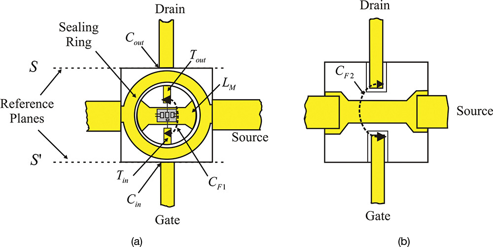
Figure 5.10 GaAs FET package assembly: (a) top view and (b) bottom view. S-parameters are usually defined at the reference planes S and S’.
The planes S and S’ shown in Figure 5.10(a) become the reference planes of the S-parameter measurement and the measured S-parameters are usually provided with these reference planes. Thus, many parasitic elements are added to the chip’s equivalent circuit in the packaged device. This is shown in Figure 5.11. The bonding-wire inductances Lg, Ls, and Ld occur as a consequence of wire bonding. In addition, since lines with a finite length are inserted into the package, they thus appear as transmission lines or inductance. Transmission lines Tin, Tout, and inductor LM in Figure 5.11 represent these transmission lines as inductance. Various parasitic capacitances also occur. Capacitances Cin and Cout occur due to the discontinuity of the transmission lines. The capacitances CF1 and CF2 represent feedback capacitances occurring as a result of the coupling between the lines in the package.
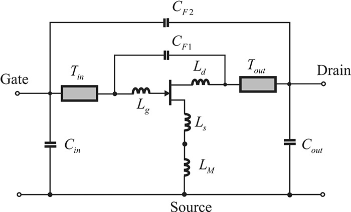
Figure 5.11 Equivalent circuit of the packaged device shown in Figure 5.10
These packaged-circuit parasitic elements prevent the accurate determination of the values of the active device’s equivalent circuit. Thus, it is common to obtain first the value of the chip’s equivalent circuit and then the value of the package’s equivalent. These are combined to yield the overall value of the equivalent circuit.
5.2.5 GaAs pHEMT
The electron mobility in the channel of an FET is closely related to its high-frequency performance. As previously explained, the GaAs FET has better high-frequency performance than the Si because the electron mobility in the GaAs is about six times faster than the Si. However, this electron mobility is usually degraded by the doped impurity atoms that are doped to generate electrons. After the generation of electrons, the impurity atoms take on + polarity while the electrons take on – polarity. The moving electrons are thus attracted and scattered by the fixed impurity atoms with + polarity. As a result, the electron mobility is significantly degraded by the impurity scattering. This electron mobility degradation can be avoided by employing a complex epitaxial layer structure instead of a single epitaxial layer. Figure 5.12 shows the complex epitaxial layer structure that improves electron mobility.
In Figure 5.12, the electrons are generated in the n-type AlGaAs layer, where impurity atoms are richly doped. The heterojunction is formed between the undoped AlGaAs and the undoped GaAs. As a result, an electron well is formed as a result of the heterojunction. The generated electrons in the n-type AlGaAs layer are then easily trapped and gathered in the electron well that is formed beneath the undoped GaAs layer. Since the electron well is very thin, the trapped electrons in the well can be considered to be a sheet of electron gas that is called 2DEG (2-dimensional electron gas). In addition, note that the undoped GaAs layer is almost intrinsic because there are no impurity atoms. Thus, the electrons can move according to the applied electric field without the influence of the impurity atoms. This results in an electron velocity that is much faster than in the GaAs FET. Therefore, the high-frequency gain performance can be improved when compared with a conventional GaAs FET because the electrons move much faster in the undoped channel. For this reason, the device is called an HEMT (high-electron-mobility transistor).
In the fabrication of a GaAs pHEMT, the lattice constants of the AlGaAs and GaAs differ significantly, making it difficult to grow a stable AlGaAs layer on the GaAs. The problem is solved by using the recently developed pseudomorphic technology. Inserting an extremely thin, undoped InGaAs layer between the undoped GaAs and the undoped AlGaAs layers, the stable AlGaAs layer can be grown, which makes it possible to manufacture these high-performance devices. Since the pseudomorphic technology is used to fabricate these devices, they are often called pHEMTs.
5.3 Bipolar Junction Transistor (BJT)
5.3.1 Operation of an Si BJT
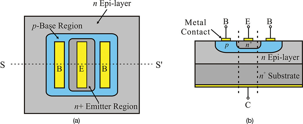
The structure of a BJT is shown in Figure 5.13, in which (a) shows the top view and (b) shows the cross-sectional view through line S-S’. As seen in the figure, first an n-type epitaxial layer is grown on the n+ substrate. Then, on the n-type epitaxial layer, the base region is formed by locally doping a p-type material. The emitter area is then formed by locally doping an n+-type material on the base region. Using this procedure, an npn BJT is formed.
The principles of operation for an npn transistor are usually explained using the dotted-line area in Figure 5.13(b), which is also shown in Figure 5.14. Two pn junctions, the base-emitter (BE) junction and the collector-base (CB) junction, appear in the transistor. The two pn junction diodes are connected back-to-back. The BJT can operate in various modes such as active, cutoff, inverse, and saturation. In the active mode, the base-emitter (BE) junction is forward-biased while the collector-base (CB) junction is reverse-biased. As a result, the barrier height of the BE junction is lowered while the barrier height of the CB junction is raised. Due to the lowered BE-junction barrier height, the majority carriers, which are the electrons in the emitter region, are diffused into the base region while the holes in the base region are diffused into the emitter region. However, because the CB junction is reverse-biased, the diffusion between the collector and base do not occur due to the increased barrier height. Normally, the emitter region is more heavily doped than the base region. Thus, more electrons will be diffused from the emitter to the base than will holes from the base be diffused to the emitter. Consequently, the current contribution from the diffusion of holes can be ignored.
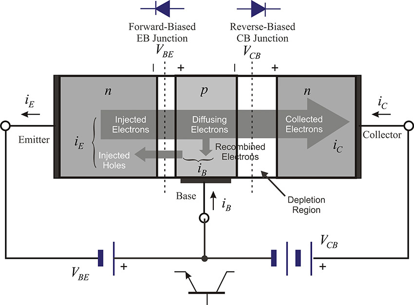
A small number of the diffused electrons from the emitter recombine and thereby disappear in the base region, while most of the electrons are collected in the collector region. Thus, the collector current iC is almost equal to the emitter current iE. Note that the emitter current iE depends on the BE junction barrier height, which in turn is controlled by a small voltage applied to the BE junction, VBE. Therefore, the large emitter current flow of the BJT can be controlled by a small-voltage VBE, which thus acts as an amplifier. Therefore, the BE-junction voltage plays a similar role to the gate voltage in an FET.
However, the structure of the BJT shown in Figure 5.13(b) needs some improvements before it can be used in a high-frequency application. Basically, high-frequency performance is closely related to the base width. First, the electrons injected from the emitter should transit the base region to reach the collector. The transit time is related to the base width. Thus, the base width should be as narrow as possible. Second, a base-spreading resistance occurs due to the distance between the true base region and the actual base terminals, as shown in Figure 5.13(b). As a result, the gain at high frequencies is reduced. The base-spreading resistance can be reduced by increasing the base-region doping. However, the significantly increased doping of the base region increases the number of holes and, consequently, the number of holes that are diffused from the base to the emitter increases. As a result, the base current increases, which is desirable. As a way of reducing the base-spreading resistance, the base and emitter are implemented using the interdigital structure shown in Figure 5.15. When the finger width and spacing of the interdigital structure are narrowed, the base-spreading resistance can be significantly reduced due to the short length between the true base region and the base terminal.
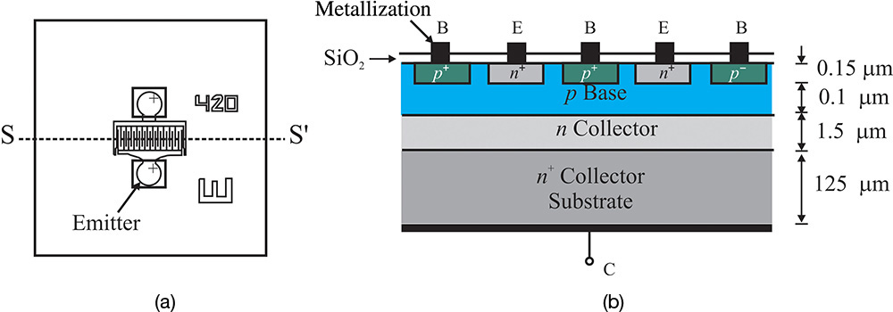
Figure 5.15 A high-frequency BJT’s (a) top and (b) cross-sectional views. The base-spreading resistance that appears between the base terminal and the true base region is reduced by using the interdigital configuration for the base and emitter. Also, the cut-off frequency fT can be made higher in order to have a shallow base region using the process control.
In addition, because the electrons should pass through the n-type epitaxial layer in order to reach the collector terminal, the epitaxial layer is made sufficiently thin in order for the electrons to arrive at the collector terminal at a much faster rate. This BJT structure is shown in Figure 5.15 and the cross-sectional structure along S–S’ is shown in Figure 5.15(b). In that figure, the base thickness typically has the order of 0.1 μm, and the n-type collector thickness typically has the order of 1.5 μm, which is extremely thin. The base and emitter spacing is found to be about 1 μm in order to reduce the base-spreading resistance.
5.3.2 Large-Signal Model of a BJT
A large-signal model of a BJT is shown in Figure 5.16. From Figure 5.14, because the BE and BC junctions can be represented by diodes, they are represented as diodes IBR and IBF in Figure 5.16. The subscript B represents the base, while the subscripts F and R stand for forward and reverse. In addition, the space-charge-region diode is known to occur in the pn junction when the junction currents are at a low level. Thus, these space-charge-region diodes appear in the BE and BC junctions, and they are connected in parallel. In Figure 5.16, they are represented by diodes ILE and ILC. It is worth noting that the collector current is not generated due to the space-charge-region diode currents, and the currents that result from these diodes can be treated as leakage currents, which is why the subscript L is added.
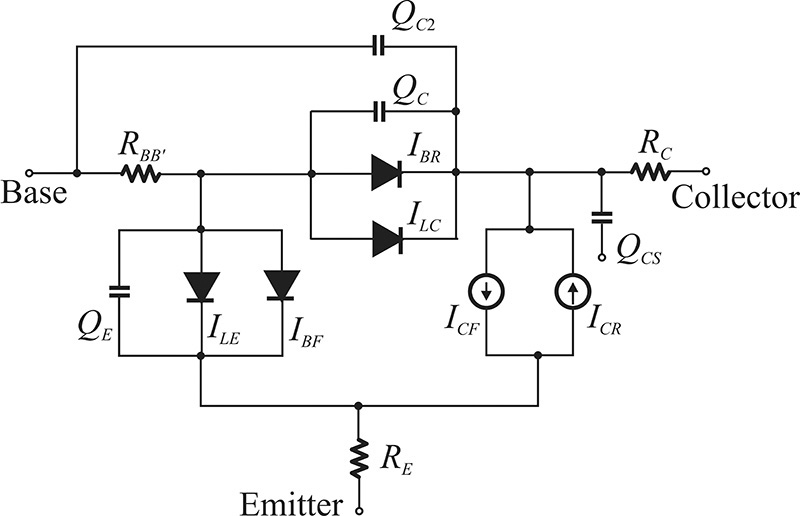
Figure 5.16 Large-signal model of a BJT. The charges QE and QC include the diffusion and depletion capacitances. ILE and ILC represent space-charge-region diodes and do not contribute to the collector current IC. IBF and ICF are the base and collector currents in the active mode, while IBR and ICR are the base and collector currents in the inverse mode. RE and RC are contact resistances, while RBB’ is the base-spreading resistance. The charge models QC2 and QCS are device dependent.
Therefore, the base current can be expressed in terms of the collector saturation current Is as follows:

The first two terms of Equation (5.11) are related to the collector current flowing when each of the BE and BC junctions are forward-biased; each of them is divided by its respective current gain, βF and βR. The last two terms represent the current of the space-charge-region diode, which is independent of the collector current.
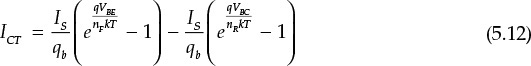
It can be seen that the current due to the BE and BC junction diodes constitutes the total collector current ICT = ICF-ICR. The current is caused by two modes: the first occurs when the BE junction is forward-biased and the BC junction is reverse-biased (active mode); the second occurs when the BC junction is forward-biased and the BE junction is reverse-biased (inverse mode). In this case, the current is in the reverse direction. Thus, the collector current ICT can be expressed as shown in Equation (5.12).
The qb in the expression is a factor that represents the Early effect and the Kirk effect that appear in a large collector current and they are expressed as follows:
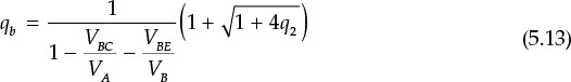
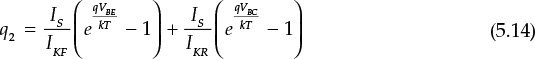
VA and VB in Equation (5.13) represent the forward and reverse Early voltages, respectively, while IKF and IKR in Equation (5.14) represent the forward and reverse knee currents of the collector current. Equations (5.11) through (5.14) represent the DC characteristics of the BJT.
Figure 5.17 illustrates how these parameters are determined. Plotting IB and IC with respect to VBE enables us to extract the BE junction-related parameters given by Equations (5.11) through (5.14). This extraction is usually called a Gummel plot. From Figure 5.17, the knee current IKF of the collector current can be determined from the turning point and from the slopes where the current begins to show. For the base current, on the other hand, the space-charge-region diode and the BE junction-related parameters can be determined from the turning point and the slopes in a small base current. Similarly, by plotting the Gummel plot for VBC the BC junction-related parameters can be extracted. The parameters are grouped and shown in Table 5.1.
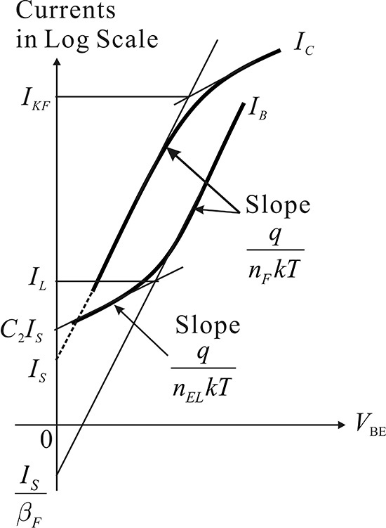
Figure 5.17 Gummel plot for VBE. The space-charge-region diode current ILE is dominant in IB for a small VBE, while IBF is dominant in IB for a large VBE. Using the slopes and intercepts, the parameters of the two diodes can be determined. The collector current IC saturates as IC increases due to the Kirk effect. Similarly, the parameters of the collector current can be determined using its slopes and intercepts. Repeating for VBC, the DC parameters for IC and IB can be completely determined.
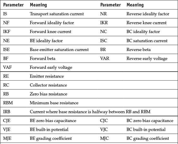
Next, we consider the resistances caused by contacts. These are RE, RB, and RC, but of these, RB is not a simple contact resistance. It varies according to the current and so two additional parameters (RBM, IRB) are required to describe it. These parameters are summarized in Table 5.1 and are classified as groups.
In addition, depletion and diffusion capacitances appear at the BE and BC junctions. The depletion capacitance is given in Equation (5.15) as
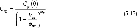
The depletion capacitance has the parameters Cje(0), mE, and φBE. They refer to the capacitance at 0 V, the grading coefficient, and the built-in potential, respectively. The parameters for the BE junction’s depletion capacitance can be determined experimentally from the C–V measurement for VBE. Through curve fitting of the measured results in Equation (5.15), the parameters can be determined. Similarly, the same parameter group can be defined for the BC-junction’s depletion capacitance and those parameters can be experimentally extracted using the C–V measurement for VBC. The parameters for the BE- and BC-depletion capacitances are also grouped and shown in Table 5.1. However, because these expressions for the BE- and BC-junction depletion capacitances have singularity at VBE = φBE and VBC = φBC, their applications are usually limited to VBE ≤ FC⋅φBE and VBC ≤ FC⋅φBC. For VBE or VBC values greater than these, a straight line that is given by the tangent at FC⋅φBE is used instead of Equation (5.15). Thus, the value FC in Table 5.1 represents the range of VBE and VBC.
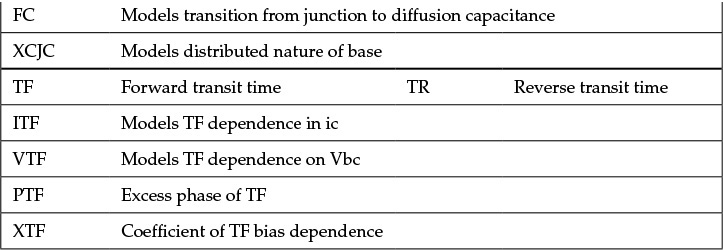
The diffusion capacitance is usually characterized by the transit time, which appears in the active and inverse mode operations. The transit time in the active and inverse mode operations is represented by TF and TR in Table 5.1, respectively. In addition, since the transit time is not constant but depends on several parameters, the parameters that represent this dependence (ITF, VTF, PTF, and XTF) form a group. The capacitors QE and QC in Figure 5.16 represent the capacitances that are the result of the previously explained depletion and diffusion capacitances. The capacitors QC2 and QCS depend on the fabrication method, and the reader may refer to reference 7 at the end of this chapter for details. Also, some additional circuit elements can be added to the BJT equivalent circuit described in this book according to the fabrication process. The reader is encouraged to consult other relevant references for details.
5.3.3 Simplified Equivalent Circuit and S-Parameters
Figure 5.18 shows a BJT small-signal equivalent circuit derived from the large-signal model in Figure 5.16. Since the BC junction is generally reverse-biased in active mode, the BC junction can be represented by the parallel RC circuit. The value of gμ comes from a reverse-biased diode and its value is usually quite small. The capacitor Cμ represents a depletion capacitance. Similarly, the forward-biased BE junction can also be represented by the parallel RC circuit. The resistor gπ represents the small-signal conductance of the forward-biased diode. Capacitor Cπ represents the combined capacitances from the diffusion and depletion capacitances. Generally, the diffusion capacitance is larger than the depletion capacitance and the value of Cπ is primarily determined by the diffusion capacitance. In a low-frequency application, the diffusion capacitance Cπ is typically small compared to gπ and so is ignored. However, in a high-frequency application, Cπ becomes dominant and the effects of both elements appear. Especially in microwave applications, the occurrence of gπ can be ignored when compared to Cπ. Transconductance gm represents the collector current controlled by the BE-junction voltage, while gc represents the resistance from the Early effect. Resistors RE, RB, and RC represent the contact resistances.
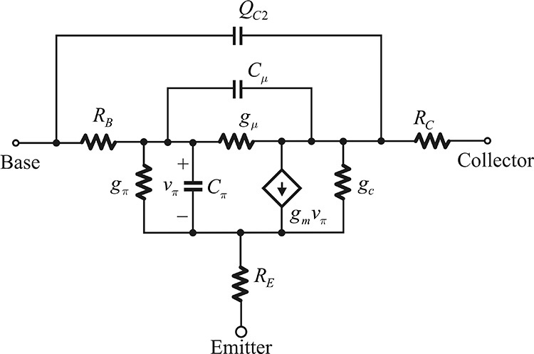
Figure 5.18 A small-signal equivalent circuit. The circuit elements gπ and Cπ represent the small-signal equivalent circuit for the BE-junction diode while gμ and Cμ represent those of the BC-junction diode. RE and RC are contact resistances, and RB is the base-spreading resistance. QC2 is the capacitance, which is device dependent.
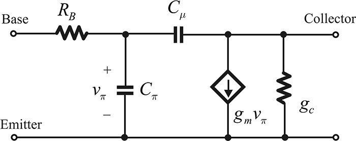
The circuit shown in Figure 5.18 is complex and can be difficult to understand. Therefore, the simplified equivalent circuit shown in Figure 5.19 is often used to explain the qualities of the measured S-parameters. The resistor gπ in the simplified equivalent circuit is ignored in a high-frequency application. Since the value of gμ is also small, it is also ignored and even Cμ is sometimes ignored. The values of RE and RC are typically small, and because they are the resistances caused by contacts, they are also ignored. The equivalent circuit thus obtained is shown in Figure 5.19.
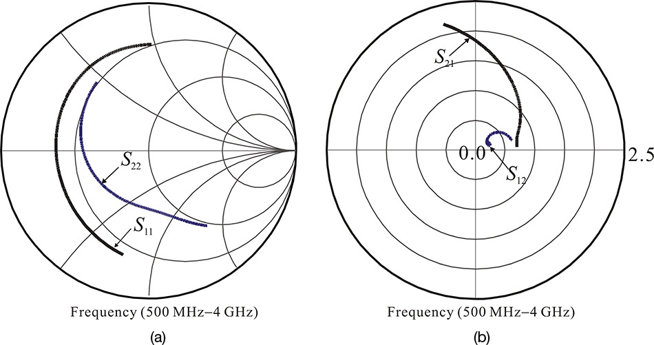
In Figure 5.20, similar to the FET, S11 and S22 are plotted on the Smith chart since they are related to impedance. In contrast, S12 and S21 are the transfer functions and so they are plotted on the polar chart to show their magnitude and phase. The radius of S21 is set to 10.0, and the radial scale corresponds to a division of 2.0 per grid. However, as S12 is small, the radial scale is selected to be 0.2 per grid.
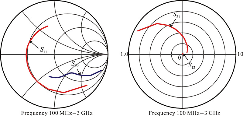
Here, as in a GaAs FET, the input impedance includes the bonding wire in the measurement. Thus, the input approximates a series RLC circuit from the simplified equivalent circuit shown in Figure 5.19. As a result, the locus of the S-parameters follows a constant resistance circle, as shown in Figure 5.20. At low frequency, the locus lies in the capacitive region of the Smith chart. However, as the frequency increases, the inductance of the bonding wire becomes dominant and so the locus lies in the inductive region. The resistance value at resonance approximately corresponds to the base resistance RB in the simplified equivalent circuit. In addition, by using the method described in Chapter 2 to compute the L and C values at resonance, both the inductance and the capacitance of the bonding wire can be obtained. The capacitance obtained can be interpreted as Cπ.
In the case of S22, because the collector resistance gc is small, the effect of gc is seldom observed in S22. Rather than gc, the output circuit can be approximated as the series connection of Cμ and rπ || (Zo + RB) for an extremely low frequency. In this case, because rπ is generally large, the output circuit appears to approximate the series connection of Cμ and (Zo + RB). Therefore, the locus moves, following the constant resistance circle. As the frequency becomes higher, the approximate output circuit appears to be gc in parallel with a parasitic capacitor Cc. Thus, with increasing frequency, the locus moves along the constant conductance circle. Due to the effect of Cc, the trajectory appears in the capacitive region. The resulting locus is the combined locus that moves along the constant resistance circle at low frequencies, and moves along the constant conductance circle at high frequencies. Even though it is not shown here, with a further increase in frequency, S22 follows a trajectory similar to that of S11 due to the effects of bonding-wire inductors and Cμ.
From the simplified equivalent circuit of Figure 5.19, S21 in Equation (5.16) is
Therefore, by using the low-frequency measurement data, the approximate value of gm can be determined. Since the voltage across Cπ decreases as the frequency increases, its magnitude decreases. It can also be seen that the phase increases in a clockwise direction. Similar to the FET explanation, we can also see in Equation (5.17) that for the low-frequency limit S12 becomes
The phase of S12 can also be seen to increase in a clockwise direction as the frequency increases. From the equation above, the magnitude also increases as the frequency increases.
5.3.4 Package
Figure 5.21 shows a typical example of a low-power BJT package.
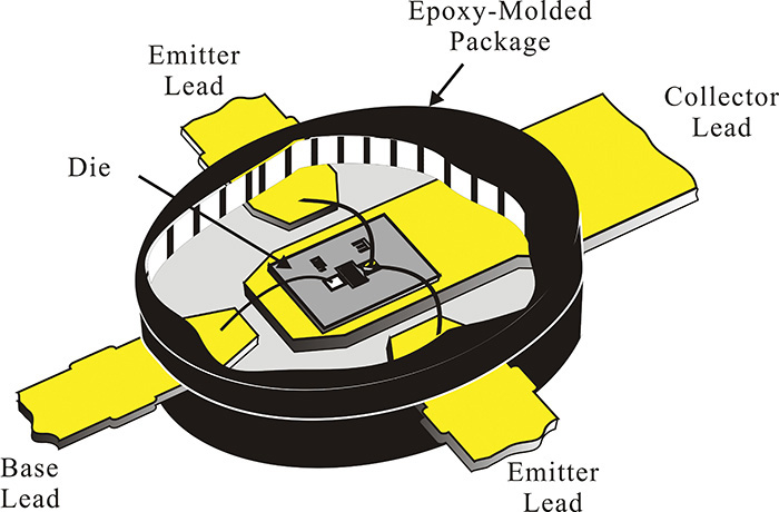
Figure 5.21 Example of a low-power BJT package. On the lead frame, the BJT chip is attached and wire-bonded. Then, the assembled BJT is molded using an epoxy material and any unnecessary lead frames are cut.
In Figure 5.21, the BJT is first attached to the lead frame. It is worth noting that the bottom of the chip generally becomes the collector, as shown in Figure 5.13(b). Then, the base and emitter terminals are wire-bonded to the corresponding lead-frame terminals. Since the parasitic elements appearing at the emitter terminal from the assembly provide feedback from output to input, they have a significant effect on device performance. In order to minimize these parasitic emitter inductances due to the assembly, it is common to assign two terminals to the emitter.
After the assembly, the wire-bonded chip is molded using an epoxy material. Then, the lead terminals are appropriately cut from the lead frame to be used as a packaged device. This packaging for a BJT will result in performance degradation at high frequencies as in the case of an FET.
5.3.5 GaAs/AlGaAs HBT
Figure 5.22 shows the cross-sectional view of a GaAs heterojunction bipolar transistor (HBT). The advantages of a compound semiconductor GaAs over an Si and the characteristics of a heterojunction are used in the GaAs HBT to improve the performance of the Si BJT. However, note that the base and emitter have the same interdigital structure that is used in the Si BJT.
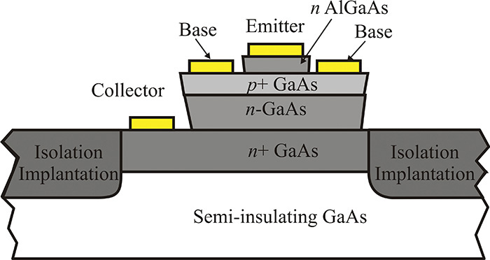
Figure 5.22 Cross-sectional structure of a GaAs HBT. The base-emitter junction is composed of the heterojunction of the AlGaAs and the GaAs, which suppresses the diffusion of the base-region holes into the emitter.
The BE junction of the GaAs HBT is formed by using the n-type AlGaAs emitter and the p-type GaAs base. Thus, an energy trap occurs between the AlGaAs and GaAs heterojunction. The energy trap is useful for suppressing the diffusing holes from the base toward the emitter that appears for a forward-biased BE junction. The diffusing holes are easily trapped and therefore the holes’ diffusion is significantly suppressed. Due to the energy trap, the doping of the base region can be increased. As a result, the base resistance at high frequencies that limits device performance can be decreased. Therefore, the unit-gain frequency given in Equation (5.18) is increased.
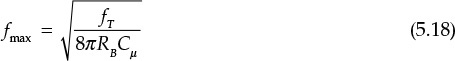
Here, fT is the cut-off frequency at which the short-circuit current gain becomes unity. The frequency fmax represents the maximum oscillation frequency at which the maximum power gain becomes unity.
As previously explained, the injected electrons from the emitter to the base arrive at the collector by diffusion. Thus, the base transit time τb is determined by the diffusion constant. The diffusion constant of electrons in the GaAs, Dn is four times larger when compared to that in the Si, and a smaller base transit time results. The base transit time τb is directly related to the cutoff frequency fT. The smaller τb results in a further increase in fmax given by Equation (5.18).
The electrons arrive at the collector then move from the collector region by a drift mechanism and finally arrive at the collector terminal. Suppose that the devices fabricated using the Si and the GaAs have the same collector thickness. The drift velocity vd of electrons in the GaAs is approximately six times faster than in the Si. As a result, the faster vd will reduce the collector transit time, τd. The reduced τd also leads to a rise in fT. Thus, due to such improvements, the GaAs HBT can be used up to 10 GHz. With more advanced processes, the GaAs HBT can be used up to the millimeter wave frequency.
5.4 DC Bias Circuits
For the use of a BJT or an FET in amplifier or oscillator circuits, it is necessary to bias it with appropriate DC sources, such as DC voltage or current sources. The DC bias circuit can determine the operating point of the BJT or FET. However, the DC bias circuit should not affect the RF signal flow. Consequently, decoupling the DC bias circuit from an RF circuit is necessary. In this section, we will discuss the DC bias circuit of microwave transistors as well as the decoupling method.
5.4.1 BJT DC Bias Circuits
5.4.1.1 DC Bias Circuit
Figure 5.23 shows two typical DC bias circuits for a BJT. In the case of the DC bias circuits in Figure 5.23(a), the approximate base current is IB = 0, and supply voltage VCC divided by the resistors R1 and R2 appears at the base. As shown in Equation (5.19), the base voltage VB is
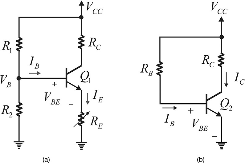
Figure 5.23 DC bias circuits; (a) circuit using emitter resistor, (b) circuit with emitter resistor removed. The circuit in (a) provides a stable IC, while the circuit in (b) provides a stable ground.
Then, Equation (5.20) finds the emitter current IE to be
Thus, the desired value of the emitter current IE is obtained by varying the resistor RE. In addition, since the RF output is usually taken from the collector, the voltage VCE will be limited by the resistor RC. In order to overcome the RF signal-swing limitation by the resistor RC, an RF choke (RFC) is often employed instead of resistor RC.
In the case of Figure 5.23(b), the base current IB is obtained from Equation (5.21) as
Thus, the collector current IC is subsequently given by Equation (5.22) as
The typically large variations in the value of β among units of the same device type appear. This will result in the large variations of the collector current IC determined by Equation (5.22) and IC may generally deviate from the design value. Consequently, the value of the resistor RB should be adjusted to obtain the desired value of the collector current IC. Compared with the DC bias circuit shown in Figure 5.23(b), the DC bias circuit that uses the emitter resistor shown in Figure 5.23(a) can yield a designed collector current insensitive to the variations in the values of β. Therefore, the DC bias circuit in Figure 5.23(b) is not generally used at low frequencies, while the DC bias circuit that uses the emitter resistor shown in Figure 5.23(a) is preferred for low-frequency applications.
However, the emitter terminal is usually grounded in an RF application, and a stable ground is needed for an RF application. When the bypass capacitor is added in parallel to the emitter resistor RE in Figure 5.23(a) for the AC ground, many problems arise due to the unstable AC ground. Practically, this type of configuration is accompanied by unpredictable, small, parasitic elements between the emitter terminal and the ground. Even assuming an ideal bypass capacitor, in order to connect the capacitor in parallel with the resistor RE, inevitably some land patterns and connection lines are required, which make it very difficult to correctly predict the impedance attached to the emitter terminal. In a worstcase scenario, the emitter’s parasitic impedance may cause oscillations or it may even significantly change the S-parameters of the BJT, which often leads to failure in obtaining the desired gain. Thus, although the circuit shown in Figure 5.23(a) supplies a stable DC collector current, this type of DC bias circuit should be avoided in an RF amplifier circuit, especially when using packaged BJTs. On the other hand, despite the flaws of the bias circuit shown in Figure 5.23(b), such as the device-to-device DC collector current change and the necessity for the adjustment of RB, the DC bias circuit is preferred in RF amplifier applications because it provides a stable RF ground.
5.4.1.2 RF Decoupling
Figure 5.24 shows the method for decoupling a designed DC bias circuit from an RF circuit. The two capacitors, CB, block the DC current flowing out to the RF input and output, and are called DC block capacitors. These capacitors are usually set sufficiently large so as to behave as shorts at the operating frequency. However, the DC block capacitors are not pure capacitors. As described in Chapter 2, parasitic elements, such as a series inductor, are inherent in the DC block capacitors. As a result, a large-valued chip capacitor may not function as a DC block at higher frequencies and can cause significant insertion loss due to the parasitic series inductor. In general, up to a frequency of a few hundred MHz, the chip capacitor operates well as a DC block because the value of the series inductor is small. However, beyond this frequency, the capacitor does not work adequately as a DC block due to the influence of the series inductor. The chip capacitors should be replaced by other capacitors to behave as a true DC block. In the case of thin-film implementation, MIM capacitors can be also used for a better DC block. The MIM capacitors can usually be connected with wire bonding. Since the bonding wires also produce inductances, the length and number of the bonding wires should be set to produce only minimal parasitic inductances. In PCB assembly, the DC block is often constructed with coupled transmission lines. However, the coupled transmission lines can usually be used as a narrowband DC block when a broadband DC block is not required. Using coupled-transmission-line DC block will avoid the effects of the imprecise parasitic inductances.
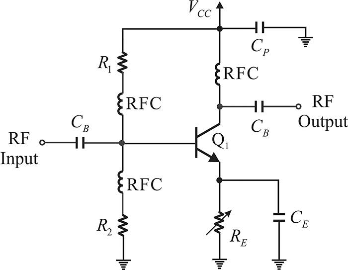
Figure 5.24 An example of an RF decoupled circuit. The RFCs connected to R1 and R2 can be removed when the values of R1 and R2 are sufficiently large. For the selection of the DC block capacitors CB, refer to Chapter 2. Bypass capacitor CP should not only provide the circuit ground but also block the incoming DC supply noise.
The next problem is the selection of the bypass capacitor CP for isolating the RF circuit from the external bias circuitry. The bypass capacitor CP, similar to the DC block capacitor, should be sufficiently large enough to behave as a short at the operating frequency. It is critical that the CP should be placed so as not to affect the RF circuit. Careful consideration should be given in advance as to whether the flow of the RF signal could be affected. Obviously, when CP is sufficiently large, the lower-frequency AC noise from the DC supply that may flow into the internal RF circuitry can be effectively blocked. However, a bypass capacitor chosen to block the low-frequency AC noise from the DC supply does not act as a short at the RF as discussed in section 2.3.1 of Chapter 2. Thus, to make a short circuit at the RF, two parallel capacitors or, occasionally, multiple capacitors in parallel are used. In this case, a small-value capacitor operating as a short at the RF and a large-valued capacitor to block the AC noise from the DC supply are selected.
In addition, the capacitor CE is inserted to provide the RF ground. Since this capacitor bypasses the emitter resistor RE, it is called a bypass capacitor. However, the bypass capacitor causes significant problems at high frequencies. A capacitor that can be a short at the RF must be chosen for CE. However, in reality it is difficult to choose such capacitor. Although such a bypass capacitor can be chosen, extra connecting lines and land patterns are necessary to connect the chosen bypass capacitor in parallel to the emitter resistor RE. As a result, the effects of the connecting lines and land patterns appear at RF and these effects should be also minimized. These effects are more pronounced as the operation frequency becomes higher and so the ground by the bypass capacitor as shown in Figure 5.24 is usually not recommended, except for oscillators and for amplifiers operating at frequencies below a few hundred MHz.
The RFC shown in Figure 5.24 acts as an open circuit at the operating frequency and opens the collector terminal. In the case of RFCs connected to the base, they open the base terminal from the bias resistors R1 and R2. In general, however, the RFC bandwidth is narrow and other resonance phenomena can appear. Note that RFCs are not necessary where a resistor can sufficiently ensure an open circuit for an RF. Thus, when resistors R1 and R2 are sufficiently large compared with the surrounding impedances, it is usually a good idea to use resistors alone without the addition of RFCs due to the broadband characteristic of the resistors. In contrast, the replacement of the collector RFC by a resistor is usually not recommended due to the DC collector current. Thus, it is necessary to use the RFC in spite of resonance and its narrowband property. In this case, the RFC is selected to resonate at the operating frequency since it opens at the resonance frequency.
5.4.1.3 Active DC Bias Circuit
Figure 5.25 shows an active DC bias circuit. Transistor Q1 is a DC-biasing low-frequency operating pnp transistor and transistor Q2 represents the RF transistor. From the circuit shown in Figure 5.25, the supply voltage VCC divided by the resistors R2 and R3 appears at the base of Q1. Thus, the base voltage VB of Q1, as shown in Equation (5.23), becomes
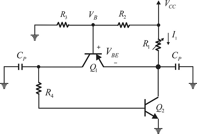
Figure 5.25 An active DC bias circuit. Q2 is an RF transistor while Q1 is a low-frequency transistor for biasing Q2.
Therefore, using Equation (5.24), a current I1
will flow through resistor R1. Current I1 is the sum of the collector current of Q2 and the emitter current of Q1. The emitter current of Q1 is equal to the base current of Q2, which is negligible compared to the collector current of Q2. Thus, I1 is approximately equal to the collector current of Q2. Therefore, we can see that the current flowing in the transistor Q2 is determined by the resistor R1 as in Equation (5.24), regardless of the β of the transistor. Note that the emitter terminal of transistor Q2 is also directly grounded and the circuit retains the two advantages of the DC bias circuits shown in Figure 5.23. The disadvantage is that the supply voltage VCC must be greater than the collector voltage of transistor Q2. This becomes a serious problem when the collector current is large because the power loss due to the collector resistor R1 is high. Bypass capacitors CP are inserted to isolate the DC bias circuit from the RF circuit. The criteria for the selection of such capacitors are the same as for the selection of the bypass capacitor CP previously described.
5.4.2 FET DC Bias Circuit Design
The unique feature of the DC bias circuit for a depletion-mode FET is that a negative voltage is necessary for the gate bias. Figure 5.26 shows two types of DC bias circuits for the depletion-mode FET.
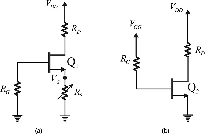
Figure 5.26 FET DC bias circuit: (a) a self-bias circuit and (b) a DC bias circuit using two DC sources. The circuit in (a) gives a stable ID while that in (b) provides the stable ground.
In Figure 5.26(a), the source resistor RS is inserted, so that when the drain current flows, a voltage drop across resistor RS appears, which is the voltage at the source VS. Since the DC current does not flow through the gate, the gate DC voltage is 0. Therefore, the voltage VGS between the gate and source is -VS. This VGS determines the drain current, which can be adjusted by changing the value of the resistor RS. If a large value is selected for RS, a large negative VGS appears and the drain current becomes small. On the other hand, when RS is small, a large drain current flows. As previously explained, since there is usually no DC current flowing in the gate, gate resistor RG has no effect. The reason for inserting the gate resistor in the circuit is to protect the device. In abnormal operation, a positive voltage may appear across the gate and a large gate current flows, which can damage the FET. To prevent this, a resistor is often inserted in the gate for protection. The circuit in Figure 5.26(a) is called a self-bias circuit.
In Figure 5.26(b), two DC voltage sources are used. A negative DC voltage is applied to the gate while a positive voltage is applied to the drain. Thus, the drain current is adjusted by voltage –VGG. The reason for inserting resistor RG in the gate is the same as for that shown in Figure 5.26(a). The resistor inserted in the drain sets the drain-source DC voltage. Resistor RD may not be needed in RF circuit applications. In addition, the pros and cons of two DC bias circuits are the same as those for the BJT DC bias circuits. Figure 5.26(a) shows a stable DC drain current, while Figure 5.26(b) shows a stable RF ground.
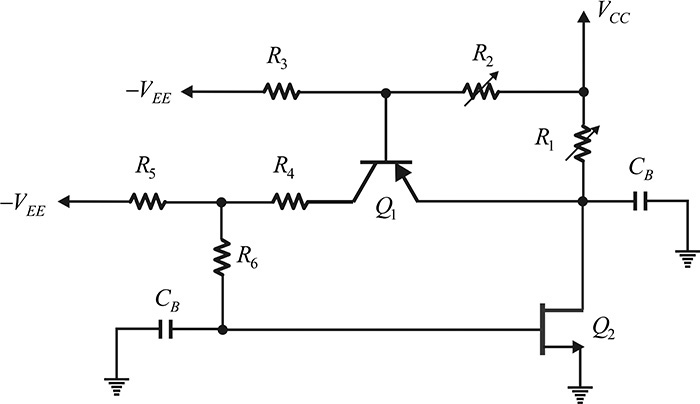
Figure 5.27 illustrates an active DC bias circuit of an FET. The transistor Q1 is a low-frequency DC-biasing pnp transistor, while Q2 represents an RF FET. The resistors R2 and R3, as in the case of the BJT active DC bias circuit, divide the supply voltage. The difference from the active DC bias circuit shown in Figure 5.25 is that both negative and positive voltages are used in the FET active DC bias circuit. The base voltage determined by the voltage division then determines the current through the resistor R1. The current through R1 is equal to the sum of the currents flowing through the transistors Q1 and Q2. Because most of the emitter current of Q1 appears at the collector, the negative voltage that results from the voltage division appears at the gate of the FET, and this determines the DC current flowing in the drain of the FET. This method for isolating the DC bias circuit is similar to that of the BJT. Also, the resistor R6 inserted in the gate is intended to protect the FET from damage when, in an abnormal operation, a large current flows as a result of possible positive voltage appearing at the gate.
5.4.3 S-Parameter Simulation
Figure 5.28 shows an example of an S-parameter simulation for an FET.
A real measurement using test equipment is similar to the same S-parameter simulation shown in Figure 5.28. The DC feed in Figure 5.28 is a component representing an RFC that becomes a short for the DC and an open for the RF. The DC block represents a component that is open at the DC and short for all the RF frequencies. The gate and drain voltages are set to VGS = –1 V and VDS = 3 V. Note that the bypass capacitors for DC voltage supplies are not necessary because the DC voltage source provides a complete short at AC.
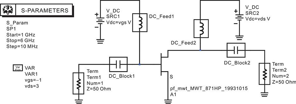
Figure 5.28 An S-parameter simulation of an FET. The component DC_Block is an ideal DC block. The DC_Block is short at AC, and open at DC. In contrast, the component DC_Feed is an ideal RFC. In the simulation, bypass capacitors for DC voltage sources are not necessary because the DC voltage sources are ideally short at AC.
Figure 5.29 shows the S-parameter simulation results. When the S-parameter simulation is performed with this setup, DC analysis will automatically be performed in advance without the need to specify it separately. At the established DC operating point, the FET will be converted automatically into the corresponding small-signal equivalent circuit, and the S-parameters of the FET will be computed. The computed S-parameters will show the previously explained frequency dependencies.
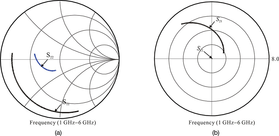
Figure 5.30 shows a BJT S-parameter simulation setup. It is similar to an FET S-parameter simulation. The only difference is that a DC current source is used for DC biasing the base. Since the operating point of the BJT is usually determined by the DC collector current, the corresponding base current is supplied by the current source. In addition, because the DC current source is open at the AC, an RFC will not be needed. The calculated S-parameters of this set up are shown in Figure 5.31.
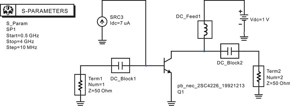
Figure 5.30 A BJT S-parameter simulation setup. Since the BJT collector current is controlled by the base current, the current source is used to bias the BJT. Note that the DC current source acts as open at the AC and the RFC in series is not necessary. The explanations for other elements are similar to those for an FET bias circuit.
5.5 Extraction of Equivalent Circuits
Physically modeled equivalent circuits rather than measured S-parameters for passive or active microwave devices sometimes provide designers with more insight for understanding those devices’ operations. Many microwave devices can be physically modeled as either T-type or π-type equivalent circuits, and their equivalent circuit element values often need to be extracted from the measured S-parameters for further analysis and design. For devices that can be modeled by T- and π-type equivalent circuits, their equivalent circuit element values can easily be extracted by converting their S-parameters to Z- and Y-parameters. Since the Z- and Y-parameters themselves can be naturally represented by T- or π-type equivalent circuits respectively, the T- and π-type equivalent circuit element values can be easily obtained from the converted Z- or Y-parameters.
Figure 5.32 shows a T-type equivalent circuit. We will show that the derivation of the T-type equivalent circuit from the Z-parameters is converted from the measured S-parameters. From the definition of the Z-parameters, the port voltages can be expressed as
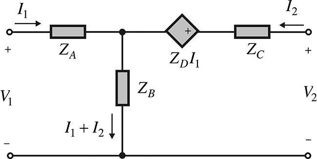
Since the voltage V1 at port 1 in Figure 5.32 depends on the currents I1 and I1 + I2, by rewriting Equation (5.25), we obtain Equation (5.27):
Thus, comparing Equation (5.27) with V1 of Figure 5.32, ZA and ZB are expressed in Equations (5.28) and (5.29).
Also, by arranging voltage V2 at port 2 as determined by I2 and I1 + I2, and arranging the remaining terms as determined by the current I1, we obtain
V2 = z21I1 + z22I2 = z12(I1 + I2) + (z22 – z12) I2 + (z21 – z12) I1
Comparing the equation above with V2 derived from the circuit in Figure 5.32 yields Equations (5.30) and (5.31).
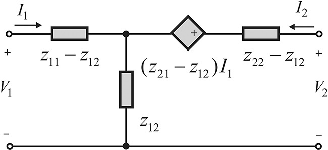
Using Equations (5.28) through (5.31), the circuit in Figure 5.32 can be represented using Z-parameters as shown in Figure 5.33.
Similarly, Y-parameters can be represented by a π-type equivalent circuit. Figure 5.34 shows a π-type equivalent circuit.
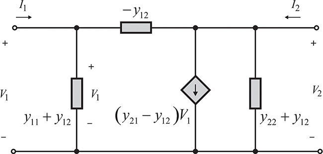
Note that when two port voltages are present simultaneously, the current flowing from port 1 to port 2 depends on the voltage difference V1 – V2. Thus, current I1 at port 1 can be expressed as
I1 = y11V1 + y12V2 = –y12(V1 – V2) + (y11 + y12)V1
Similarly, current I2 at port 2 can be expressed as
I2 = y21V1 + y22V2 = –y12 (V2 – V1) + (y22 + y12) V2 + (y21 – y12) V1
Using the two equations above, we can obtain the π-type equivalent circuit shown in Figure 5.34.
The equivalent circuits in Figure 5.33 and Figure 5.34 are general examples and can be further simplified for passive devices. The equivalent circuit for a passive device is shown in Figures 5.35(a) and (b), respectively. By the reciprocity z12 = z21 and y12 = y21 in the Z- and Y- parameters, the controlled sources disappear in the passive device’s equivalent circuits.
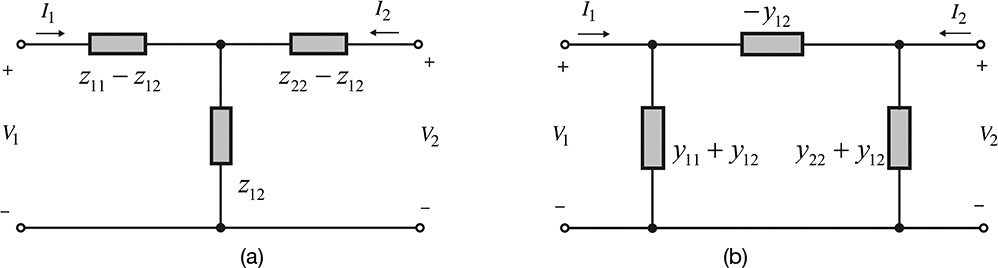
The equivalent circuits in Figures 5.35(a) and (b) are useful for analyzing unknown inductors or capacitors. Practically speaking, (z11 – z12), z12, and (z22 – z12) in the T-type equivalent circuit, and (y11 + y12), y12, and (y22 + y12) in the π-type equivalent circuit may not be represented by a single element such as an inductor or a capacitor, and they may show a frequency dependence. In this case, the frequency dependence of each element can be further decomposed and represented by the complex circuit that consists of frequency-independent elements, as explained in Chapter 2. In addition, using a similar technique, a multiport passive device can be represented in a similar way. The reader may wish to consult reference 8 at the end of this chapter for details.
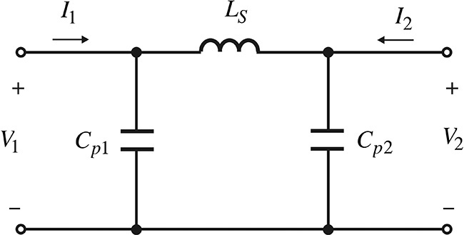
For a 10-mil-thick alumina substrate with a permittivity of 9.6, a microstrip ring inductor that has 2 turns, width and spacing of 10 mil, and an inner radius of 50 mil can be represented by the equivalent circuit in Figure 5E.1 for frequencies up to 2 GHz. Calculate the values of the equivalent circuit. Here, Ls represents the inductance that results from the microstrip ring-type inductor, and Cp1 and Cp2 represent the parasitic capacitances.
Solution
Figure 5E.2 shows the S-parameter simulation setup for the microstrip ring-type inductor.
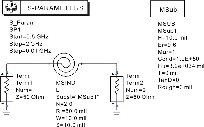
Figure 5E.2 S-parameter simulation of a microstrip ring-type inductor. The S-parameters as well as the Y- or Z-parameters can be obtained simultaneously after the S-parameter simulation. The parameters N, Ri, W, and S represent the number of turns, the inner radius, and the width and spacing of the spiral inductor MSIND.
Before calculating the S-parameters, open the S-parameter simulation controller in ADS, and check the Y-parameter calculation in the Parameters tab. This setting provides the S-parameters as well as the Y-parameters to be stored in the dataset after the simulation. The following equations shown in Measurement Expression 5E.1 are then entered in the display window. The values of Ls, Cp1, and Cp2 are plotted with respect to frequency and are shown in Figure 5E.3.
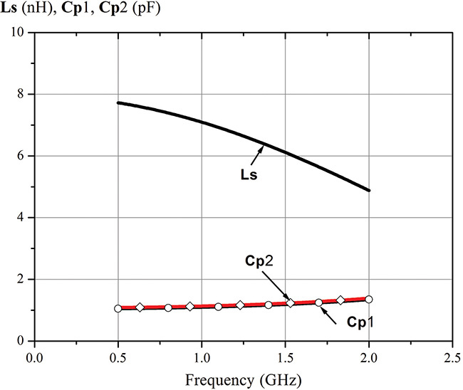
Figure 5E.3 Capacitances Cp1 and Cp2, and the series inductance of a microstrip ring-type inductor. In most cases, the number of significant digits is two, so the scale of the y-axis is set to vary from 0–10.
![]() w=2*pi*freq
w=2*pi*freq
![]() Cp1=(imag(Y(1,1)+Y(1,2)))/w
Cp1=(imag(Y(1,1)+Y(1,2)))/w
![]() Cp2=(imag(Y(2,2)+Y(1,2)))/w
Cp2=(imag(Y(2,2)+Y(1,2)))/w
![]() Ls=-1/imag(-Y(1,2))/w
Ls=-1/imag(-Y(1,2))/w
Measurement Expression 5E.1 Equation for calculating the value of the equivalent circuit values in Figure 5E.1
Cp1 in Measurement Expression 5E.1 represents the shunt capacitor at port1, while Cp2 represents the shunt capacitor at port 2. The inductor Ls represents the series inductor that connects port 1 and port 2. Note that Cp1 and Cp2 are almost frequency independent. However, Ls shows some frequency dependence. Thus, Ls cannot be represented by a single inductor and should be represented by a more complex circuit.
We now present the method for obtaining the values of the simplified small-signal equivalent circuit shown again in Figure 5.36(a) from the measured S-parameters.2 The π-type equivalent circuit in Figure 5.36(b) is similar to the simplified equivalent circuit of an FET. Therefore, by directly matching the simplified FET equivalent circuit to the π-type equivalent circuit, the values of the simplified equivalent circuit can be directly obtained from the measured S-parameters. First, comparing the output impedances of the two circuits in Figures 5.36(a) and (b), the admittance of Rds||Cds should be equal to y22 + y12. From this comparison, we obtain Equations (5.32) and (5.33).
2. K. W. Yeom, T. S. Ha, and J. W. Ra, “Frequency Dependence of GaAs FET Equivalent Circuit Elements Extracted from the Measured Two-Port S-parameters,” Proceedings of the IEEE, vol. 76, no. 7, pp. 843–845, July 1988.
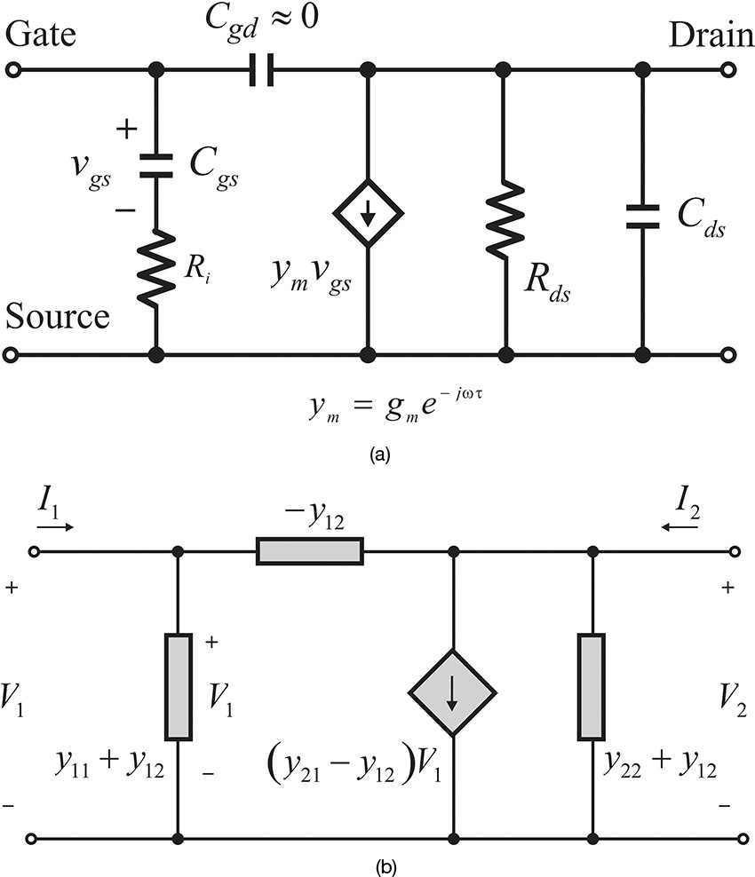
Figure 5.36 (a) A GaAs FET simplified equivalent circuit and (b) a Y-parameter equivalent circuit. The two representations look similar and the only difference is in the control voltage: in (a), the control voltage appears across Cgs, while in (b) V1 is the control voltage.
Similarly, comparing y12 and Cgd, we obtain Equation (5.34).
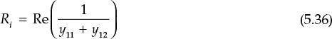
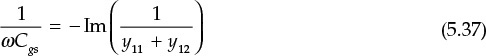
Comparing the input impedances of the two circuits, we obtain Equation (5.35).
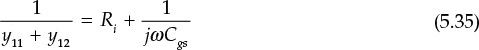
Rewriting Equation (5.35), Ri and Cgs can be determined using Equations (5.36) and (5.37).
However, the control voltages are different in the dependent sources shown in Figures 5.36(a) and 5.36(b). In the case of Figure 5.36(a), voltage Vgs across Cgs is the control voltage, while in the case of Figure 5.36(b), the control voltage is V1. The relationship between V1 and Vgs is
Also,
(y21 – y12) V1 = ym Vgs
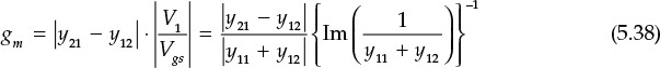
Using these two equations, gm can be obtained with Equation (5.38).
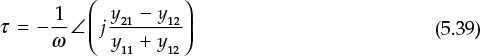
And τ is determined with Equation (5.39).
Using Equations (5.32) through (5.39), we find that the values of the simplified equivalent circuit of FET can be directly determined from the measured S-parameters.
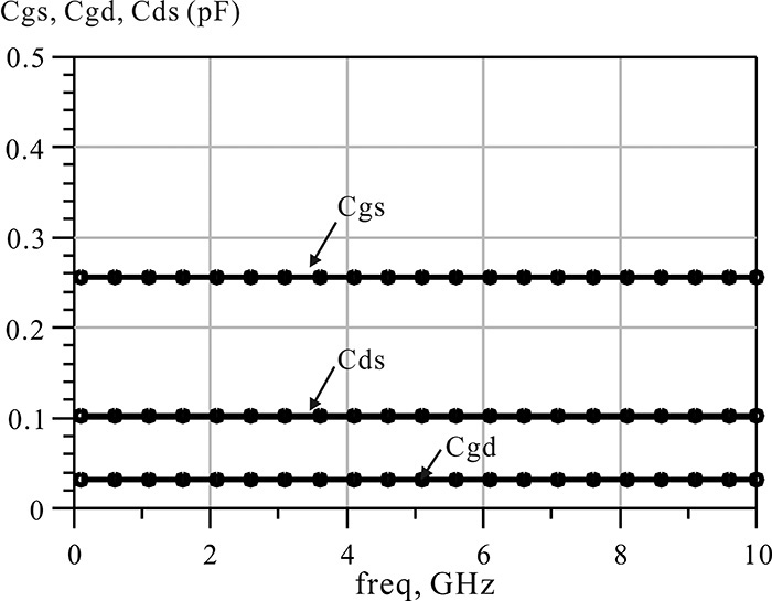
This example shows how to obtain the simplified FET equivalent circuit. Open the model of the chip pHEMT FHX15 in the ADS library and compute the S-parameters at VDS = 2 V and VGS = –0.2 V. Using the S-parameters, compute the simplified FET equivalent circuit element values.
Solution
Figure 5E.4 shows a DC simulation setup. The ID–VDS characteristics are plotted in Figure 5E.5. From the ID–VDS characteristics, the drain current can be found to be IDS = 18 mA at VDS = 2 V and VGS = –0.2 V. Setting VGS and VDS for IDS = 18 mA, the S-parameter simulation is performed as shown in Figure 5E.6. To obtain the simplified FET equivalent circuit element values using the obtained S-parameters, the following equations shown in Measurement Expression 5E.2 are entered in the display window.
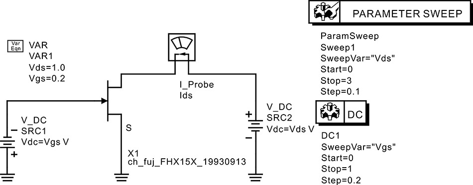
Figure 5E.4 DC simulation circuit to determine the drain current IDS. The current probe Ids measures the simulated drain current. The ParamSweep sweeps Vds from 0 to 3 V and the DC simulation component sweeps Vgs from 0 to –1 V.
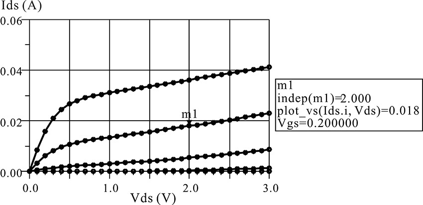
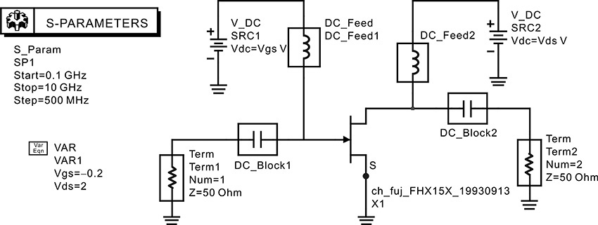
Figure 5E.6 S-parameter simulation setup. To yield IDS = 18 mA, Vgs = -0.2 V, Vds = 2 V are applied. Note that the Y-parameters are computed simultaneously using the S-parameter simulation.
![]() Cgd=imag(-Y(1,2))/w
Cgd=imag(-Y(1,2))/w
![]() Rds=1/real(Y(2,2)+Y(1,2))
Rds=1/real(Y(2,2)+Y(1,2))
![]() Cgs=-1/(w*(imag(1/Y(1,1)+Y(1,2))))
Cgs=-1/(w*(imag(1/Y(1,1)+Y(1,2))))
![]() Cds=1/w*imag(Y(2,2)+Y(1,2))
Cds=1/w*imag(Y(2,2)+Y(1,2))
![]() Ri=real(1/Y(1,1)+Y(1,2)))
Ri=real(1/Y(1,1)+Y(1,2)))
![]() gm=-mag((Y(2,1)-Y(1,2))/(Y(1,1)+Y(1,2)))/imag(1/(Y(1,1)+Y(1,2)))
gm=-mag((Y(2,1)-Y(1,2))/(Y(1,1)+Y(1,2)))/imag(1/(Y(1,1)+Y(1,2)))
![]() tau=(-1/w)*phase(j*(Y(2,1)-Y(1,2))/(Y(1,1)+Y(1,2)))
tau=(-1/w)*phase(j*(Y(2,1)-Y(1,2))/(Y(1,1)+Y(1,2)))
Measurement Expression 5E.2 Equations for obtaining the values of the simplified equivalent circuit
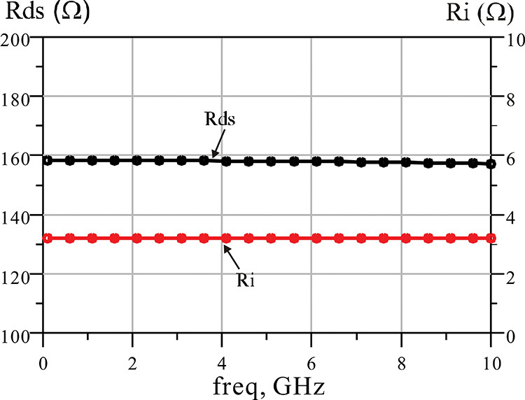
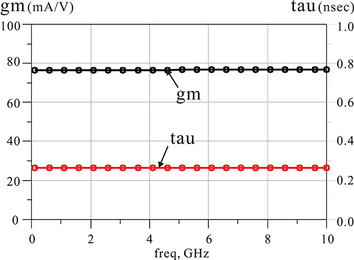
Figures 5E.7 through 5E.9 show plots for the equivalent circuit element values with respect to frequency. From these figures, we find that gm = 77 mA/V, τ = 0.26 ns, Rds = 158 Ω, Cgs = 0.25 pF, Cgd = 31 fF, and Cds = 0.1 pF.
From Example 5.2, we can determine the simplified FET equivalent circuit element values. Figure 5.37 again shows the equivalent circuit of a chip FET. The equivalent circuit is known to predict quite closely the measured S-parameters of a chip FET.
The difference between the chip FET and the simplified equivalent circuits is in Rg, Rs, and Rd, which are called extrinsic elements. A method for determining the chip FET equivalent circuit element values, which is similar to the extraction of the simplified equivalent circuit, does not exist at present. The values of Rg, Rs, and Rd were previously determined by optimization, which yields the best fit to the measured S-parameters. However, because resistors Rg, Rs, and Rd in the active state of a FET make only a small contribution to the S-parameters, there is significant uncertainty about their values when determined by this method, and obtaining their exact values is difficult.3 If we assume that Rg, Rs, and Rd do not change even when the DC operating point changes, their values may be determined more accurately using the measured S-parameters at other DC operating points where their effects are dominant. Thus, such operating points should be found first, after which their values can be extracted more accurately.
3. R. L. Vaitkus, “Uncertainty in the Values of GaAs MESFET Equivalent Circuit Elements Extracted from the Measured Two-Port Scattering Parameters,” presented at the 1983 IEEE Cornell Conference on High Speed Semiconductor Devices and Circuits, Cornell University, 1983.
The operating points of VGS = 0 V and VDS = 0 V are thought to be suitable for the extraction of Rg, Rs, and Rd. At this bias point, the FET completely becomes a passive device, and the equivalent circuit appears, as shown in Figure 5.38. The zero-bias depletion capacitance Cb appears, and will appear on both the source and drain sides. Because there is no change in the values of Rg, Rs, and Rd, their values are the same as in active mode. The measurement at VGS = 0 V and VDS = 0 V is often referred to as a cold-FET measurement.4 Even in the cold FET condition, because the values of Rg, Rs, and Rd are typically small, and the impedance of the depletion capacitance Cb is usually very large, it is difficult to determine their values accurately when measurement errors occur.
4. G. Dambrine, A. Cappy, F. Helidore, and E. Playez, “A New Method for Determining the FET Small-Signal Equivalent Circuit,” IEEE Transactions on Microwave Theory and Techniques, vol. 36, no. 7, pp. 1151–1159, July 1988.
Figure 5.38 FET small-signal equivalent circuit for VGS = 0 V and VDS = 0 V. Since VDS = 0 V, the same depletion capacitance appears between the gate drain and the gate source.
To overcome this problem, a small positive voltage is applied to the gate terminal, which makes the gate drain and gate source behave like Schottky diodes. The Schottky diodes then begin to conduct for a small positive voltage and so the contribution of Cb disappears. Instead, a small-signal resistance of a Schottky diode appears. In addition, the channel resistance is formed between the drain and source terminals. Since the effect of the channel resistance appears in a distributed form, it must be considered as a distributed circuit. However, the circuit’s distributed effect is not pronounced and so it can be regarded as a lumped element. With the channel resistor considered, the Z-parameters are expressed in Equations (5.40)–(5.42).
Resistor Rc represents the channel resistance, and nkT/qIg of z11 represents the small-signal Schottky diode resistance that is dependent on the DC gate current Ig. The different contributions of Rc to z11, z12, and z22 are because the effect of the distributed channel resistance yields different contributions to z11, z12, and z22. From Equations (5.40) through (5.42), we find that only z11 depends on the small-signal Schottky diode resistance. Thus, the term that excludes the small-signal Schottky diode resistance can be found by plotting Re(z11) versus Schottky diode current Ig. Figure 5.39 shows a plot of Re(z11) versus Ig. Using this plot, the term that excludes the small-signal Schottky diode resistance in Equation (5.40) can be found from the intercept value obtained by extrapolating the straight line.
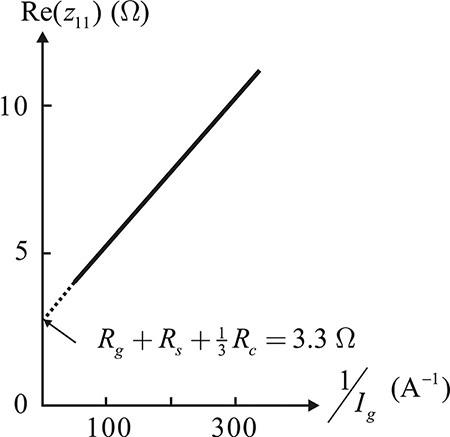
Figure 5.39 Plot for obtaining Rg + Rs + 1/3·Rc (drawn after the reference).6 The z11 represents the Z-parameters of the forward-biased cold FET.
However, using Equations (5.40) through (5.42), the values of Rg, Rs, and Rd cannot be determined because there are four unknowns but only three available equations. Therefore, a separate independent measurement is necessary. There are two methods: The first is to use the Fukui method, with which the value of Rs + Rd can be determined.5 The second is to directly measure the DC gate resistance in a device. Then, the values of Rg, Rs, and Rd can be determined.
5. H. Fukui, “Determination of the Basic Device Parameters of a GaAs MESFET,” Bell System Technical Journal, vol. 58, no. 3, pp. 771–795, March 1979.
6. G. Dambrine, A. Cappy, F. Helidore, and E. Playez, “A New Method for Determining the FET Small-Signal Equivalent Circuit,” IEEE Transactions on Microwave Theory and Techniques, vol. 36, no. 7, pp. 1151–1159, July 1988.
Using the obtained values of Rg, Rs, and Rd, the remaining values of the chip FET equivalent circuit in Figure 5.37 can be determined from the measured S-parameters in active mode. Figure 5.40 shows the method for removing the contribution of resistors Rg, Rs, and Rd from the measured S-parameters in the active mode. Then, the remaining circuit is a simplified FET equivalent circuit (or intrinsic equivalent circuit of an FET). By converting the resulting S-parameters into Y-parameters, the values of the simplified equivalent circuit can be determined, as shown in Example 5.2.
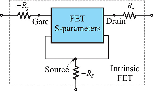
Figure 5.40 The method for removing the effects of resistors Rg, Rs, and Rd in the measured S-parameters. The added three resistors with – values remove the effects of the resistors Rg, Rs, and Rd on the S-parameters and the S-parameters of the intrinsic FET can then be obtained.
In Example 5.2, the values of Rg, Rs, and Rd were approximated to 0 in order to extract the simplified FET equivalent circuit of the pHEMT FHX15 at VDS = 2 V and VGS = –0.2 V. When Rg = 1.4, Rs = 1.5, and Rd = 1.5 Ω, determine the values of the simplified FET equivalent circuit element values with the effects of resistors Rg, Rs, and Rd removed.
Solution
Figure 5E.10 shows a circuit setup to remove the effects of resistors Rg, Rs, and Rd. In Figure 5E.10, the S-parameter data component SNP1 represents the S-parameters used for computing the simplified equivalent circuit element values in Example 5.2. Similar to Example 5.2, the check box of the calculation of Y-parameters in the S-parameter simulation controller SP1 is checked.
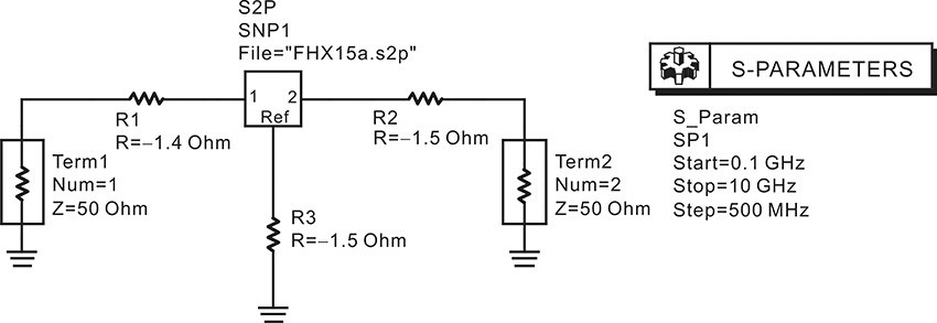
The formulas in Measurement Expression 5E.2 are entered again in the display window and then the changes in the values of the simplified FET equivalent circuit element values can be obtained. The computed values of the simplified equivalent circuit are gmo = 88 mA/V, τo = 0.25 ns, Rdso = 137 Ω, Cgso = 0.28 pF, Cgdo = 29 fF, and Cdso = 0.12 pF. The general trend is that the resistance values decrease while the capacitor values increase. The frequency dependences of the computed results are not appreciable, and the values simply move up and down. The change in the transconductance is especially noteworthy as it is directly related to the gain. It can be seen that the change Δgm = gmo - gm = 11 mA/V. The comparison is shown in Figure 5E.11.
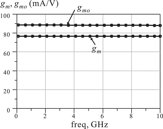
In Figure 5E.11, gmo represents the compensated result for Rg, Rs, and Rd, while gm represents the value in the previous example, which does not take into consideration the effects of resistors Rg, Rs, and Rd. Here, it is generally known that Rs is the main reason for the reduction in gmo and gmo is reduced by Rs as in
We can see that Δgm is the same as was calculated in Example 5.2. Therefore, in order to prevent the reduction of gmo by Rs in a large transconductance FET, special attention must be taken to make Rs smaller.
5.6 Summary
• Three-terminal devices, FETs and BJTs, have advantages over various one-port devices in the implementation of complex-functioning integrated circuits.
• The principles of operation for small- and large-signal models, and for the typical S-parameters of GaAs MESFET are introduced.
• A GaAs pHEMT has multiple epi-layers and its electron mobility in a channel is improved by removing the impurity scattering that occurs in a GaAs MESFET.
• The base width of a high-frequency Si BJT is minimized to the limit that the process allows and the interdigital structure is employed to implement the base and the emitter in order to reduce the base-spreading resistance.
• The operations of small- and large-signal models, as well as the typical S-parameters of BJT, are explained.
• In a GaAs HBT, the base-emitter junction is implemented using a heterostructure. As a result, the current gain β is not degraded for high base-region doping, which makes it possible to implement small base-spreading resistance. The diffusion in p-type GaAs is faster than that in an Si, which results in the improvement of fT. Also, the collector drift is reduced because the electron mobility is faster than that in an Si. Combining these facts, the high-frequency performances of the GaAs HBT are superior to those of the Si BJT.
• Self-bias and two-supply DC bias circuits are introduced. The two-supply DC bias circuit has an advantage over the self-bias circuit in providing a stable ground.
• The extraction of a GaAs FET equivalent circuit from S-parameters is explained.
References
1. G. D Vendelin, A. M. Pavio, and U. L. Rohode, Microwave Circuit Design Using Linear and Nonlinear Techniques, Hoboken, NJ: John Wiley & Sons, Inc., 1990.
2. G. Gonzalez, Microwave Transistor Amplifiers: Analysis and Design, 2nd ed. Englewood Cliffs, NJ: Prentice Hall, 1997.
3. R. Soares, J. Graffeuil, and J. Obregon, Applications of GaAs MESFETs, Dedham, MA: Artech House, Inc., 1983.
4. J. M. Golio, Microwave MESFETs and HEMTs, Dedham, MA: Artech House, Inc., 1991.
5. J. Mun, ed., GaAs Integrated Circuits, Oxford: BSP Professional Books, 1988.
6. H. Fukui, ed., Low-Noise Microwave Transistors and Amplifiers, New York: IEEE Press, 1981.
7. G. Massobrio and P. Antognetti, Semiconductor Device Modeling with SPICE, 2nd ed. New York: McGraw-Hill, Inc., 1993.
8. N. Marcuvitz, Waveguide Handbook, Vol. 2 of the MIT Radiation Laboratory Series. New York: Dover Publications, Inc., 1965.
Problems
5.1 Figure 5P.1 shows a simplified equivalent circuit of a low-frequency GaAs MESFET.
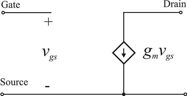
(1) Calculate the S-parameters setting the reference impedance to Zo.
(2) Setting Zo = 50 Ω, compute gm when S21 = 5∠180°.
(3) When resistor Rf is connected in parallel, as shown in Figure 5P.2, find the value of Rf that makes S11 = 0.
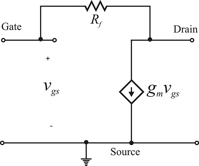
5.2 Figure 5P.3 shows a simplified equivalent circuit of an FET with a source resistance Rs at low frequency. Due to Rs, the equivalent transconductance gme is lowered from gm, as explained in Example 5.3. Defining the equivalent transconductance gme as
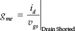
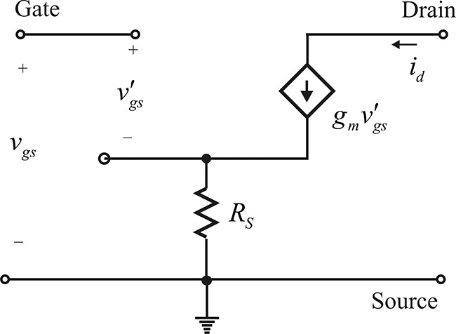
show that
5.3 The small-signal equivalent circuit of a GaAs MESFET, including wire bonding, can be approximately represented by Figure 5P.4; given the following S11, determine the values of Ri and Lg. (Cgs = 0.5 pF).
5.4 In the following active DC bias circuit (Figure 5P.5), determine the value of resistor R1 for a 20 mA current to flow into the collector of transistor Q2.
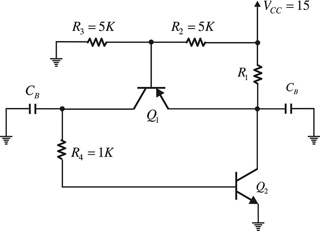
5.5 (ADS problem) Using the 2SC4226 in the ADS library, set up the circuit shown in Figure 5P.6 below.
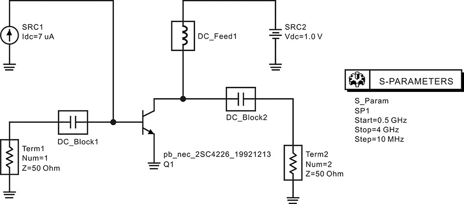
Figure 5P.6 Circuit of problem 5.5
(1) Determine its IC–VCE characteristics as shown in Figure 5P.7. (IB = 20 μA – 160 μA, with a step of 20 μA.)
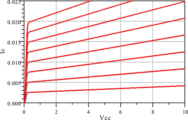
(2) Compute the S-parameters at VCE = 5 V and IC = 5 mA for a frequency range of 1–4 GHz with a step of 0.05 GHz.