
Chapter 9. Power Amplifiers
9.1 Introduction
A power amplifier is generally located just before the antenna, and determines the transmitting power level of a communication system. The design of a power amplifier is significantly different from that of the low-noise amplifier presented in Chapter 8. To demonstrate the difference, suppose that two amplifiers are designed with the same active device; one is based on the small-signal design presented in Chapter 8 and has the maximum small-signal gain; the other produces the maximum output power based on the large-signal design that will be presented in this chapter. Figure 9.1 shows a plot of the delivered power PL of the two amplifiers versus the input power Pin.
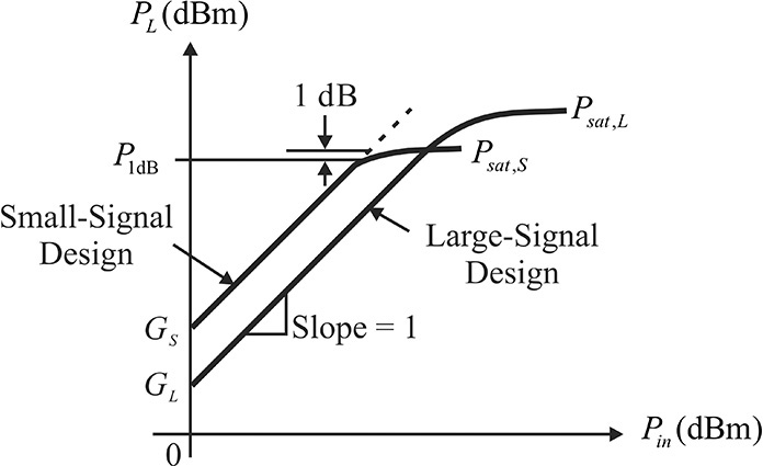
Figure 9.1 Comparison of PL – Pin characteristics of low-noise and power amplifiers. The small-signal design has a higher gain GS than the gain GL of the large-signal design; however, the small-signal design saturates early at a lower input power than does the large-signal design.
As shown in Figure 9.1, at a low input power Pin, the output power PL increases in proportion to the input power. However, at a high input power, the output power shows a marginal increase. A further increase in the input power drives the output power of the amplifier into saturation. A point with a 1-dB deviation from the linear output power is referred to as the 1-dB compression point of an amplifier and the output power level at saturation is called the saturated power of an amplifier. As discussed in Chapter 8, an amplifier with maximum small-signal gain can be designed by selecting appropriate source and load impedances computed from the measured small-signal S-parameters at a given DC bias. The designed maximum small-signal gain amplifier generally gives a high gain but also has a lower 1-dB compression point and saturated power compared to an amplifier designed to give maximum output power as shown in Figure 9.1. This is not a special case but a general fact.
To explain this qualitatively, a simplified large-signal FET equivalent circuit is shown in Figure 9.2. Here, the current source IDS, which depends on the gate-source and drain-source voltages, has the characteristics shown in Figure 9.3. In addition, excluding the current source IDS, all the other elements in the equivalent circuit of Figure 9.2 are assumed to be linear elements since they typically have low nonlinearity.
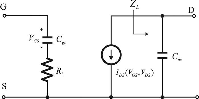
Figure 9.2 Simplified large-signal FET equivalent circuit. Here, the current source IDS represents the DC IDS–VDS characteristics of an FET.
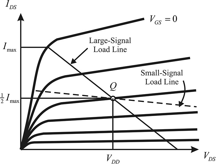
The maximum small-signal gain at the operating point Q can be achieved when the load is conjugate matched to the output impedance. Thus, the impedance ZL of Figure 9.2 must satisfy ZL = rDS = (∂IDS/∂VDS)–1. This causes the load line to have a slope of (rDS)–1, as shown in Figure 9.3. However, the load line that gives maximum output power is obviously the load line represented by the solid line in Figure 9.3. Since the gain is approximately proportional to gmRL, the gain of the amplifier based on the small-signal design is clearly higher than that based on the large-signal design. Yet the amplifier based on the small-signal design has a low saturated power and it generally reaches saturation early as shown in Figure 9.1. The small-signal design clearly does not exploit the maximum output power capability that the active device can supply.
Figure 9.4 shows a power amplifier configuration. The power amplifier can be represented by a block diagram that is similar to a low-noise amplifier. Therefore, the source and load reflection coefficients ΓS and ΓL,opt must be determined by experimental or theoretical means in order to design the power amplifier. When ΓS and ΓL,opt have been determined, the matching circuit can be constructed similar to that of the low-noise amplifier design. The slight difference between the power amplifier and the low-noise amplifier designs is that the input matching circuit losses must be minimized in the case of the low-noise amplifier design, whereas in the power amplifier design, it is the output matching circuit losses that must be minimized. The input matching circuit losses in the low-noise amplifier are directly associated with noise-figure degradation. By denoting the loss at the input matching circuit as L(dB) and the noise figure of the active device as F(dB), then the noise figure of the low-noise amplifier as explained in Chapter 4 is approximately given by L + F(dB). Thus, for a minimum noise figure, the input matching circuit must be constructed so as to have minimum losses. On the other hand, because the loss in the output matching circuit is directly related to the loss in the output power, the loss in a given output matching circuit must be minimized in the case of the power amplifier.
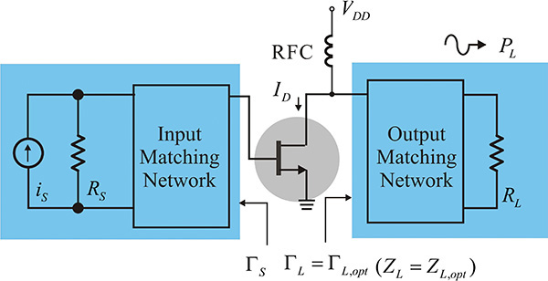
Figure 9.4 Power amplifier block diagram and its design concept. ΓL,opt is chosen for optimum output power and then ΓS is determined for the chosen ΓL,opt for conjugate matching at the input.
The impedance ZL,opt in Figure 9.4 that gives maximum output power can easily be inferred from the DC characteristics in Figure 9.3 at low frequency; however, at high frequency, due to the complexity of the equivalent circuit of the active device and the parasitic elements of its package, it is not easy to derive ZL,opt analytically. In a case where the large-signal equivalent circuit is known, the optimum impedance ZL,opt can be obtained at the reference plane of the current source IDS in Figure 9.2. Using ZL,opt, the optimum impedance at the output terminals of the package can also be obtained by taking the external parasitic elements into consideration. However, unlike at low frequency, the reference plane of the current source IDS in the large-signal equivalent circuit is generally not obvious at high frequency. Thus, ZL,opt is usually determined experimentally through a load-pull measurement or with simulation; that is, load-pull simulation using software when the large-signal model is available. We will cover the determination of ZL,opt using load-pull measurement and simulation in this chapter.
The next important issue in the implementation of a power amplifier is efficiency, which can be expressed in terms of RF output power for a given supplied DC power, and two definitions are widely used. The first is the collector or drain efficiency. Denoting the DC power consumed in the output terminal as PDC and the RF output delivered to the load as PL, the drain efficiency ηD is defined as shown in Equation (9.1).
Here, VDD represents the DC supply voltage and ID is the DC supply current when the delivered power to the load at RF is PL. To some extent, the drain efficiency may be a good measure for representing the efficiency of an amplifier when the amplifier gain is sufficiently high; however, the gain is usually not high enough at a high frequency. Consequently, the input power Pin must be considered in the definition of the efficiency. In general, PAE (power-added efficiency) is used in the definition of efficiency at a high frequency and it is defined in Equation (9.2).
This definition of PAE can be interpreted as the ratio of the output power added by the active device to the DC power supplied to the active device.
Given that VDD = 5.8 V, ID = 400 mA, Pin = 23 dBm, and Pout = 33 dBm, determine the drain efficiency and the PAE.
Solution
Since 33 dBm corresponds to 2 W, the drain efficiency is
An input power of 23 dBm corresponds to 0.2 W; therefore the PAE is
The DC biased amplifier shown in Figure 9.3 is usually classified as a class-A amplifier; the problem with this type of amplifier is that its maximum efficiency does not exceed 50%; that is, for the maximum output as shown in Figure 9.3, the approximate drain efficiency can be seen to be
In order to understand the efficiency problem in a class-A amplifier, consider an example of this amplifier with a 20 W RF output power. Even if its efficiency is given as the maximum value of 50%, out of the total 40 W power supplied, 20 W is consumed while 20 W is delivered to the load. This will be more problematic in the absence of any RF input power. The total supplied DC power of 40 W to the active device would be consumed by that device in the absence of the RF input power, and all the supplied DC power would be converted into heat. Therefore, power consumption of the class-A amplifier is most problematic in the case where there is no RF input power. This problem can be solved by changing the active device’s operation and there are various operation techniques for improving efficiency, which we will discuss in the next sections. However, designing the amplifier to improve its efficiency generally gives rise to the problem of distortion. Therefore, for a communication system that employs both amplitude- and phase-modulated signals, it is necessary to reduce the distortion to improve the amplifier’s linearity. The methods for improving linearity will also be explained in this chapter.
9.2 Active Devices for Power Amplifiers
Microwave active devices have already been discussed in Chapter 5. Of these, pHEMTs and HBTs were noted as having excellent high-frequency characteristics. To employ these devices in power amplifiers, their structures must be expanded to handle a large output power. They can be used as power devices by expanding the gate width in the case of a pHEMT or the emitter area in the case of an HBT. This will increase their output power capability, but their breakdown voltage is basically low, which limits their application as high-power devices. In addition to these devices, there are other types of high-power active devices that are widely used today. Among these, GaN (gallium nitride) HEMTs and LDMOSFETs (laterally diffused MOSFETs), simply referred to as LDMOS, have attracted a lot of attention as active devices for power amplifiers, and they will also be introduced in this chapter.
9.2.1 GaN HEMT
The important parameters of semiconductor properties for a high-power active device are electron mobility, energy band-gap (band-gap), and thermal conductivity. Among these parameters, electron mobility can be used as a criterion to estimate the high-frequency applicability of an active device fabricated using a given semiconductor process. In other words, for two active devices fabricated using the same processing method but on different semiconductors, the active device using the semiconductor with a higher electron mobility generally yields a higher gain and it can be used in applications up to higher frequencies in contrast to a semiconductor with a lower electron mobility. Thermal conductivity is an important parameter of semiconductor properties for power amplifier application. The higher the thermal conductivity, the greater the advantage is in heat dissipation. A device fabricated with a higher thermal conductivity will have a higher power consumption capability. The energy band-gap, which is simply referred to as the band-gap parameter, is closely related to the breakdown voltage of an active device. The larger the band-gap is, the higher the breakdown voltage will be. Thus, the higher band-gap semiconductor is advantageous in the fabrication of power devices.
The energy band-gap is defined as the difference in energy between the conduction band and the valence band. Thus, a higher-energy band-gap means the valence-band electrons can seldom move into the conduction band because those electrons require energy sufficiently higher than the energy band-gap to move into the conduction band. On the other hand, when the energy band-gap is low, the valence-band electrons can easily move into the conduction band as they can readily attain the required energy. The energy band-gap is thus an important measure for estimating the breakdown voltage of an active device for a given semiconductor material. The breakdown voltage refers to drain or collector voltages where the drain or collector current increases very rapidly. Therefore, the useful range of an active device’s drain voltage is usually limited by the breakdown voltage.
The phenomenon of breakdown can be explained using electron collisions. The electrons accelerated by an applied drain voltage collide with atoms at the drain, thereby generating electrons. When a drain voltage higher than the breakdown voltage is applied, the generated electrons thus attain sufficient energy to move into the conduction band and contribute to the drain current. As a result, the drain current increases rapidly due to the contribution of electrons generated by the collision. However, when the energy band-gap is high, the electrons generated by the collision with the accelerated electrons cannot attain sufficient energy to move into the conduction band. Thus, a high-energy band-gap semiconductor is typically associated with a high breakdown voltage. Due to this fact, when an active device is fabricated with a high-energy band-gap semiconductor, the active device shows a high breakdown voltage; a high DC bias voltage can then be applied and a large output power will be obtained. Therefore, a high-energy band-gap semiconductor is suitable for use as a high-power active device.
Thermal conductivity represents a material’s ability to conduct heat. A higher thermal conductivity means the heat generated in an active device due to power consumption is easily dissipated. As we have seen previously, no matter how well a power amplifier is designed, a portion of the supplied power is consumed as heat. The heat generated increases the temperature of the active device, which can damage the device if the heat exceeds the absolute maximum temperature for the device. A well-designed heat-dissipation structure such as a heat sink may help an active device endure a certain temperature increase, but the amount of heat dissipated will be fundamentally limited by the thermal conductivity of a given semiconductor. Therefore, thermal conductivity is an important parameter for the semiconductor materials used in power amplifiers.
The physical properties of various semiconductors are shown in Table 9.1. In that table, SiC and GaN have an excellent thermal conductivity compared with Si. Because the thermal conductivity of Si is comparable to that of a metal, SiC and GaN semiconductors are known to have a fairly good thermal conductivity. In contrast, GaAs has a lower thermal conductivity than Si by a factor of about one third. Thus, in terms of thermal conductivity, Si, GaN, and SiC semiconductors are suitable for the fabrication of active devices for a power amplifier. Next, in terms of an energy band-gap, SiC and GaN have a higher energy band-gap than Si by a factor of about 3. As a result, the fabricated active devices that use SiC and GaN show a breakdown voltage 3 times higher than that of Si. As a direct measure of breakdown voltage, the breakdown voltage in Table 9.1 is directly related to the breakdown voltage that is approximately 6 times larger in SiC and GaN compared to Si. Thus, a high DC supply voltage is possible with SiC and GaN, which leads to an increase in output power capability.
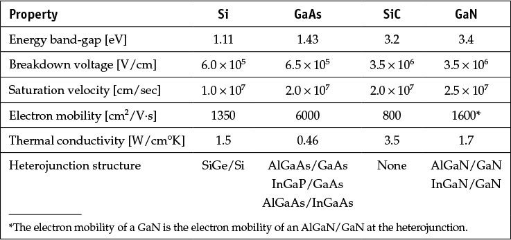
Therefore, it can be seen that SiC and GaN are suitable semiconductors for a power amplifier’s active devices, considering their thermal conductivity and energy band-gap. However, the electron mobility of SiC is lower compared to that of Si, and thus SiC active devices are inferior to Si active devices in high-frequency applications. Fortunately, the electron mobility in GaN depends on the condition of the heterojunction formation and this mobility can be made to exceed that in Si by using the heterojunction. An active device suitable for a high-frequency power amplifier can therefore be fabricated using a GaN process. Despite the GaN advantages, the late emergence of GaN devices is due to the lack of a suitable substrate for GaN growth. Recently, the technology for epitaxial-layer growth of GaN on SiC has seen significant advances, and the study of GaN-active devices continues to attract great interest.
Figure 9.5 shows the structure of a GaN HEMT formed on SiC. The reason for selecting an HEMT structure is primarily related to the electron mobility of GaN. As this mobility is not much superior to that of Si, its maximum exploitation is required. By employing an HEMT structure, maximum electron mobility can be obtained because that mobility in the channel can be achieved in the absence of impurities, as discussed in Chapter 5. The frequency characteristics of GaN active devices can therefore be improved although the electron mobility of GaN is not greatly superior to that of Si.

Figure 9.5 Structure of a GaN HEMT. To reduce the gate metallization resistance and gate length, a T-shaped gate metallization is used. An AlGaN/GaN heterojunction is formed for the maximum exploitation of the electron mobility of GaN.
In Figure 9.5, an intrinsic GaN epitaxial layer is grown on SiC, on top of which an n–type AlGaN layer is formed for the heterojunction. The electron well created by the heterojunction is formed in the epitaxial layer of the intrinsic GaN, and the doped electrons in the AlGaN are collected in the electron well and thus move through a channel free from impurity atoms. Therefore, great improvement in the frequency characteristics is possible. The T-shaped gate terminal on the n–AlGaN layer in Figure 9.5 minimizes the resistance of the gate terminal and decreases the gate length, and thus improves the frequency characteristics. Note that the drain and source terminals are formed on the n+ GaN layer for ohmic contact.
Figure 9.6(a) is a photograph of a GaN HEMT. The breakdown drain voltage VDS is reported to be 142 V. This is an advantage that results from the physical properties of a GaN semiconductor. Figure 9.6(b) shows the measured output characteristics of the GaN HEMT at a frequency of 9.3 GHz. The device shows a gain of about 14 dB, and a saturated power of about 35.7 dBm. The PAE is found to be about 40% at 35.7 dBm. The output power per unit gate width is estimated to be 3.7 W/mm.
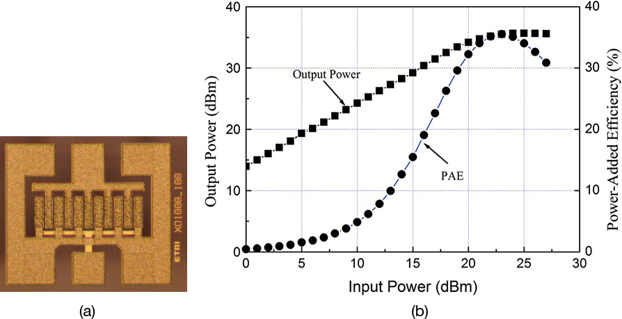
Figure 9.6 (a) Photograph of a GaN HEMT XO1000_100. The gate length and width are 0.25 μm and 1000 μm, respectively. The back side is polished to a thickness of 100 μm. (b) Output power characteristics are at 9.3 GHz. Source: (private communication): ETRI IT Convergence and Component Technology Research Section, 218 Gajeongro Yuseonggu, Daejeon, 305-700, Korea, www.etri.re.kr/kor/main/main.etri.
The frequency characteristics of a 0.25-μm GaN HEMT from Cree, Inc., are shown in Figure 9.7. In that figure, the frequency fmax is approximately 50 GHz where the maximum power gain U in Chapter 8 is 1. The frequency fT is near 20 GHz where the short-circuit current gain h21 is 1. The fmax and fT are comparable to the frequency characteristics of a GaAs MESFET. Considering the performances given in Figures 9.6 and 9.7, which were obtained from the initial stages of the GaN process, significant improvements are expected in the future.
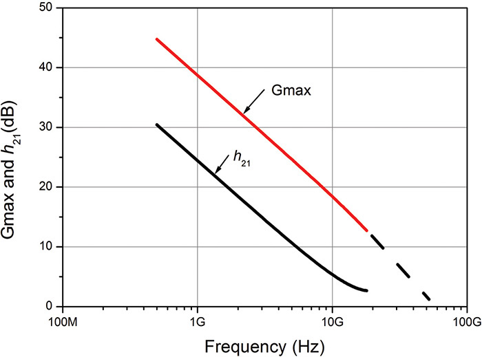
Figure 9.7 GaN HEMT frequency characteristics (refer to the datasheet).1
1. Cree, Inc., datasheet, CGHV1J006D (the S-parameters are at VDS = 40 V, IDS = 60 mA); available at www.cree.com/RF/Products/General-Purpose-Broadband-40-V/Discrete-Bare-Die/CGHV1J006.
9.2.2 LDMOSFET
An LDMOSFET (laterally diffused MOSFET) is an active power device fabricated using Si process technology and it has a structure designed to improve the breakdown voltage of an MOSFET. As explained earlier, the channel electrons attain sufficient energy at a high drain voltage VDS and they collide with the atoms in the drain region with high impurity doping for ohmic contact. Numerous electrons are generated due to the collision and these electrons gain the energy sufficient to move into the conduction band taking the relatively small Si band-gap energy into consideration. Thus, there is a sudden increase in the drain current and, as a result, the lower breakdown voltage appears. This lower breakdown voltage can be improved by adjusting a doping profile in the drain region.
Figure 9.8 shows a cross-section of the LDMOSFET. In that figure, the drain region is laterally divided into a lightly doped region (NHV) and highly doped region (n + Drain) for the ohmic contact. In addition, the drain terminal is located at a considerable distance from the channel, which causes the accelerated electrons in the channel to primarily collide in the drain region with a low impurity concentration; as a consequence, the electrons lose energy when they reach the n+ drain region. Thus, this leads to a higher breakdown voltage compared with the case in which the electrons collide directly in the highly doped drain region.
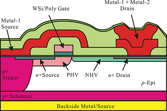
Figure 9.8 Cross-section of an LDMOSFET.2 PHV is a high-voltage p-region; NHV is a high-voltage n-region with a low n-type doping concentration (drawn per the literature identified in the footnote).
2. Motorola, Semiconductor Technologies for RF Power F701, 2002.9.24.
The next thing to note is that the source terminal is attached to the bottom of the device, which means that wire bonding is not required to connect the source terminal to the ground. A simple die attachment on the metal carrier is sufficient for the connection of the source terminal to the ground. Thus, the inductance that would otherwise arise from the wire bonding during packaging assembly is eliminated, which is an advantage during assembly. Figure 9.9 shows the electric-field simulation around the drain terminal that has a strong electric field across the NHV region, while the n+ drain region can be seen to have a weak electric field. As a result, the generation of electrons by collision occurs primarily in the lightly doped NHV region, where the number of those electrons is relatively smaller. This leads to a higher breakdown voltage than in the case of direct collision.
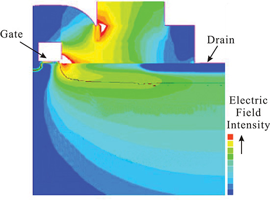
Figure 9.9 Electric-field simulation at the drain terminal of the LDMOSFET shown in Figure 9.8 (drawn per the literature.3) Note that the simulated electric-field intensity at the drain terminal becomes weak.
3. Ibid.
The manufacturing technology for LDMOSFETs is well-established. An LDMOSFET device that can supply up to several hundred W of RF power has been reported in the literature. However, the physical properties of Si limit its operation below the 4-GHz frequency region as the gain becomes low.
9.3 Optimum Load Impedances
In designing the power amplifier, the first problem is determining optimum load impedance. The reason for naming the optimum impedance, rather than the maximum output power impedance, is that the design goal can be set for maximum efficiency or other parameters, depending on the design conditions, and the optimum load impedance does not necessarily give the maximum output power.
In designing a low-noise amplifier, the optimum source and load impedances can be calculated directly from the measured small-signal S-parameters at a given DC bias. However, because the power amplifier basically operates in the large-signal region, the optimum load impedance cannot be determined using the small-signal S-parameters. Therefore, the optimum load impedance is determined either from direct experimental measurement or computed from the large-signal model prior to creating the power amplifier design. In this section, we will describe the method of obtaining the optimum load impedance by the experimental method as well as by a computational method that uses software.
9.3.1 Experimental Load-Pull Method
Load-pull measurement refers to measuring an active device’s efficiency or output power by varying the load impedance. An impedance tuner is generally used to vary the load impedance. As mentioned earlier, the optimum load impedance of a power amplifier cannot be obtained from the measured small-signal parameters. Thus, the load impedance connected to the active device’s output is tuned using an impedance tuner, and the optimum load impedance is obtained. This is referred to as a load-pull measurement. Figure 9.10 shows two impedance tuners that are inserted before and after the active device, and the source and load impedances are tuned under a given input power to obtain the optimum output power. In this method, the input tuner is first adjusted to deliver maximum power from the signal source to the input of the active device, after which the output tuner is adjusted to deliver maximum output power to the load. Once the adjustments are completed, the impedance tuners are disassembled and the desired load and source reflection coefficients ΓS and ΓL,opt are obtained by measuring the impedances of the impedance tuners. The spectrum analyzer and power meter connected to the output impedance tuner in Figure 9.10 make it possible to measure the exact value of the output power while simultaneously observing the output spectrum in the spectrum analyzer. The power meter can accurately measure the output power but it cannot detect the presence of spurious signals, which necessitates the use of the auxiliary spectrum analyzer. Nonharmonic spurious signals often occur at the output of the power amplifier but the power meter cannot distinguish whether or not the nonharmonic spurious signals occur, which is why the spectrum analyzer is required. Thus, the spectrum analyzer is included for observing the spurious signals.
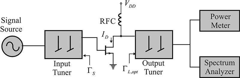
Figure 9.10 Load-pull setup. The output power is accurately measured by the power meter and the spectrum analyzer checks for the occurrence of spurious signals in the output signal.
In the case of low harmonics, the optimum load impedances can easily be obtained from the previous load-pull measurement. However, a problem does occur when the harmonic impedances must be considered. In general, the maximum output power is determined from the load impedance of the fundamental frequency, but the efficiency varies according to the harmonic load impedances. Recently, an impedance tuner that can independently tune the harmonic load impedances in order to resolve the harmonic tuning problem has been reported in the literature. A photograph of a harmonic impedance tuner is shown in Figure 9.11. Most recent impedance tuners can also be controlled by a PC, and their impedances can be read without disassembling them from the load-pull setup for the impedance measurement. The PC-controlled impedance tuners also provide utilities that draw a contour plot of the impedance, yielding the same output power or efficiency from measured data. Measuring the optimum source and load impedances using the load-pull method assists in the convenient and reliable design of power amplifiers.
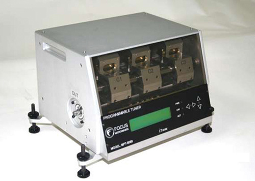
Figure 9.11 Photograph of an impedance tuner with three carriages. The three harmonic impedances can be separately controlled using this impedance tuner. Source: Focus Microwaves Inc., Three Carriage Three Harmonic Tuner, January 2012.
There is another method for designing and fabricating power amplifiers experimentally without relying on load-pull measurements. An example of this method is shown in Figure 9.12. Using this method, a power amplifier’s design allows for adjustable input and output matching circuits that use the optimum impedances in the datasheet, and the power amplifier is designed by adjusting the input and output matching circuits with a given RF input power and DC bias. Once the required specifications such as output power, efficiency, harmonic characteristics, and intermodulation are met, then the adjusted power amplifier can be used as a power amplifier if there are no other problems in size and mass production. However, the size of the power amplifier may be too large for some applications and further miniaturization may be required for those applications. Unlike the power amplifier shown in Figure 9.12, a power amplifier without tuning points may also be necessary for mass production. In those cases, the power amplifier shown in Figure 9.12 is disassembled and the source and load impedances are measured with a network analyzer as in a load-pull measurement. A miniaturized power amplifier can then be redesigned using the measured impedances.
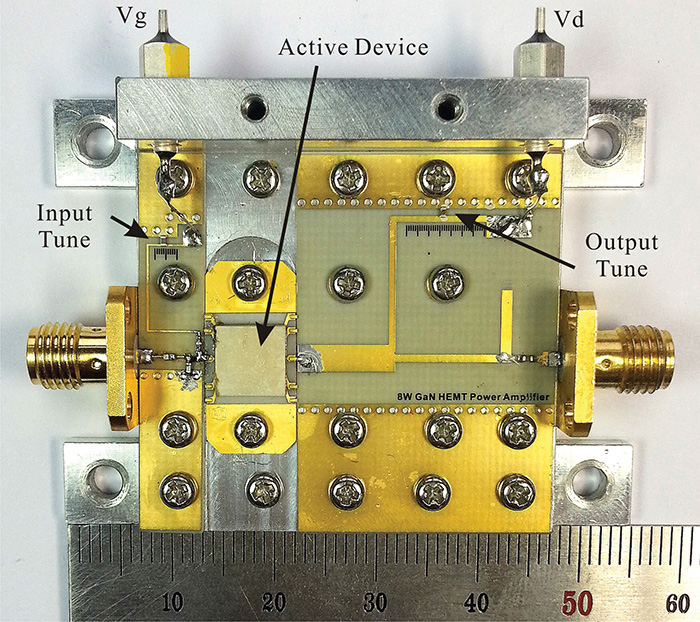
Figure 9.12 Experimental design of an adjustable power amplifier. The location and value of the chip component can be varied for the input and output matchings.
In Figure 9.12, the chip capacitor in the input matching circuit is for input tuning and its position and value can be moved by soldering. Thus, the input matching circuit can be adjusted by trial and error until the optimum input impedance is obtained. The output matching circuit can be similarly adjusted. Thus, the output matching can be achieved through these adjustments.
The advantage of the adjustable circuit impedances is that the power amplifier can be designed without the cumbersome task of modeling the active devices, so the characteristics of the fabricated power amplifier can be determined experimentally, which otherwise would be difficult to predict accurately with the large-signal equivalent circuit. The disadvantage is that because the adjustable range of the input and output matching circuit impedances is limited compared to that in the prescribed load-pull measurement, the input and output matching circuits must be designed to provide the desired input and output matching impedances. Otherwise, the designated goal cannot be achieved. In addition, when changes occur in the DC operating point or input power for a new power amplifier, the obtained input and output matching impedances are not generally optimal for those changed conditions. Therefore, to obtain the optimum input and output impedances when those conditions change, the adjustable power amplifier in Figure 9.12 should be retested using the method discussed above that includes adjusting component values and positions. In the case of mass production, tolerance analysis may also be necessary; however, this method can present difficulties in terms of predicting the effects of parameter changes in an active device or in power amplifier’s matching circuits.
9.3.2 Load-Pull Simulation
An alternative method for obtaining the optimum source and load impedances is the load-pull simulation based on the large-signal model of an active device.
When the large-signal model of an active device is available, this method involves setting up a load-pull simulation circuit in ADS, as shown in Figure 9.13, and calculating the desired optimum source and output load impedances; see reference 1 at the end of this chapter. This approach is frequently used in the design of an MMIC (monolithic microwave integrated circuit) power amplifier.
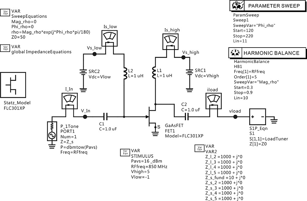
Figure 9.13 Load-pull simulation in ADS. The load impedance is adjusted using the S1P Equation component. The value LoadTuner of the S1P Equation component is determined using the variable block named globalImpedanceEquation, which is hidden. The LoadTuner value is two-dimensionally swept by the Parmeter Sweep and Harmonic Balance simulation components.
However, in the case of a packaged active device, the equivalent circuit should take into account the parasitic elements that occur in packaging and may cause the equivalent circuit to become extremely complex and may degrade its accuracy. The advantage that the load-pull simulation method has over the experimental load-pull method is that the optimum source and load impedances can be obtained simply through simulation that reflects the changes that may occur in the power amplifier’s circuit conditions, such as frequency and the DC bias operating point. In contrast, with the experimental load-pull method, each time the power amplifier’s condition changes—for example, if the frequency is changed—a new measurement must be taken to obtain the optimum source and load impedances. The disadvantage is that because it is not easy to obtain the accurate large-signal model, the large-signal model itself includes a certain degree of inaccuracy, which makes the accuracy of the results problematic.
9.3.2.1 Load Impedance
In Figure 9.13, the input frequency RFfreq is 850 MHz and input power Pavs is 10 dBm. Inductors L1 and L2 function as an RFC because their values are set to 1 μH. The values have been set sufficiently large for the chosen frequency. The DC-block capacitors C1 and C2 have values of 1 μF, which is also sufficiently large. Port 1 is the input port that has an impedance of Z_s and a power level of Pavs. The function dbmtow(·) converts the power level expressed in dBm to W. An impedance tuner implemented as a one-port circuit is connected to the output of the active device. In Figure 9.13, Z_l_2, Z_l_3, Z_l_4, and Z_l_5 of VAR2 are the load impedances at the harmonic frequencies of 2fo, 3fo, 4fo, and 5fo, respectively. By altering the harmonic load impedances, the efficiency or output power of the power amplifier can be tuned. Similarly, Z_s_2, Z_s_3, Z_s_4, and Z_s_5 are the source impedances at the harmonic frequencies of 2fo, 3fo, 4fo, and 5fo, respectively. The harmonic source impedances are also adjustable. The value of the source impedance at the fundamental frequency Z_s_fund is set to 10 Ω. The frequency-dependent source and load reflection coefficients are defined using the variable block globalImpedanceEquations shown in Measurement Expression 9.1, which is not shown in the schematic window because of its complexity.
![]() VAR
VAR
global Impedance Equations
;Tuner reflection coefficient
LoadTuner=LoadArray[iload]
LoadArray=list(0,rho,fg(Z_l_2),fg(Z_l_3),fg(Z_l_4),fg(Z_l_5))
iload=int(min(abs(freq)/RFfreq+1.5,length(LoadArray)))
fg(x)=(x-Z0)/(x+Z0)
;Source impedances
Z_s=SrcArray[isrc]
SrcArray=list(Z0,Z_s_fund, Z_s_2, Z_s_3,Z_s_4, Z_s_5)
isrc=min(iload,length(SrcArray))
Measurement Expression 9.1 Source and load impedance setup
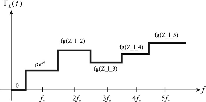
Measurement Expression 9.1 is the opened view of the globalImpedanceEquations. The value of LoadTuner here represents the resulting load impedance. The function fg(∙) is defined to convert the given harmonic load impedances into the corresponding reflection coefficients. The row vector, LoadArray, is formed using the converted reflection coefficients at each harmonic frequency. The function list(∙) is used to form a vector. Here, the first value of the LoadArray is the reflection coefficient at DC and the second value is the reflection coefficient at the fundamental frequency. All the values are set this way up to the fifth harmonic. It should be noted that the load impedance is open at DC because the reflection coefficient at DC is set to 0. The reflection coefficient of the fundamental frequency in LoadArray is set to rho, which is defined by the variable block named SweepEquations in Figure 9.13.
Figure 9.14 shows the desired frequency-dependent load reflection coefficient. Thus, the load reflection coefficient is ΓL = ρejφ for frequency 0.5fo < f < 1.5fo. The ranges of other harmonic frequencies are defined similarly to the fundamental frequency. The variable LoadTuner in Measurement Expression 9.1 represents the frequency-dependent load reflection coefficient shown in Figure 9.14 and it is synthesized using the row vector LoadArray.
In Measurement Expression 9.1, the frequency-dependent load reflection coefficient LoadTuner is implemented using the index of the row vector LoadArray. The variable iload represents the index. Define k as expressed in Equation (9.3).
When 0.5 × RFfreq < freq < 1.5 × RFfreq, the range of k is 2 < k < 3 from Equation (9.3). Also, it can be found that length(LoadArray) = 6. A smaller value between the two values for length(LoadArray) and k is selected using the min(∙) function. For 2 < k < 3, the smaller value becomes k. Thus, taking the integer part of k and using the int(∙) function gives a value of 2. Therefore, the value of iload becomes 2. The value of LoadTuner = LoadArray[iload] is the value corresponding to the index 2, which is ΓL = ρejφ. When 4.5 × RFfreq < freq, it becomes k > 6 from Equation (9.3). The smaller value thus becomes length(LoadArray) = 6. The corresponding reflection coefficient to index 6 is found to be fg(Z_l_5). With similar reasoning, it can be found that the frequency-dependent reflection coefficient LoadTuner shown in Figure 9.14 is synthesized.
It can be seen that the source reflection coefficient is determined in a similar way in Measurement Expression 9.1. The variable Z_s represents the frequency-dependent source reflection coefficient. The variable SrcArray is the row vector of the source reflection coefficients at each harmonic. The index that determines the value of the source reflection coefficient is isrc. It should be noted that the value of SrcArray at DC is set to the reference impedance Z0.
9.3.2.2 Sweep
In Figure 9.13, the sweep of the load reflection coefficient is performed using harmonic balance simulation and parameter sweep. The variable rho that represents the load reflection coefficient at the fundamental frequency consists of Mag_rho and Phi_rho. The magnitude Mag_rho varies from 0.1 to 0.9, while the phase Phi_rho varies from 120° to 220°. This variation in the reflection coefficient is shown in Figure 9.15(a). However, the density of samples decreases as the radius approaches 1, thereby reducing the accuracy in the output power and efficiency contour plots. Instead, even though Figure 9.15(b) is somewhat complex in setting the sweep parameters, a region of the circle in the Smith chart can be uniformly sampled, which is advantageous when drawing more accurate contour plots for output power and efficiency. The simulation schematic for the samples shown in Figure 9.15(b) is shown in Figure 9.16.
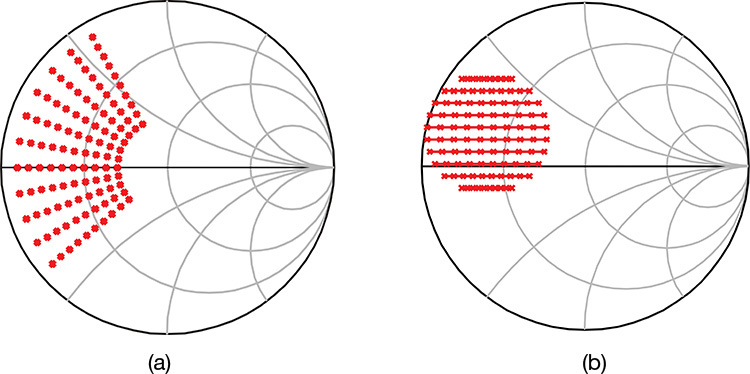
Figure 9.15 Reflection coefficient sweeping methods: (a) samples obtained using the magnitude and angle method (polar sweep) and (b) uniform sampling of a region of the circle (uniform sample sweep)
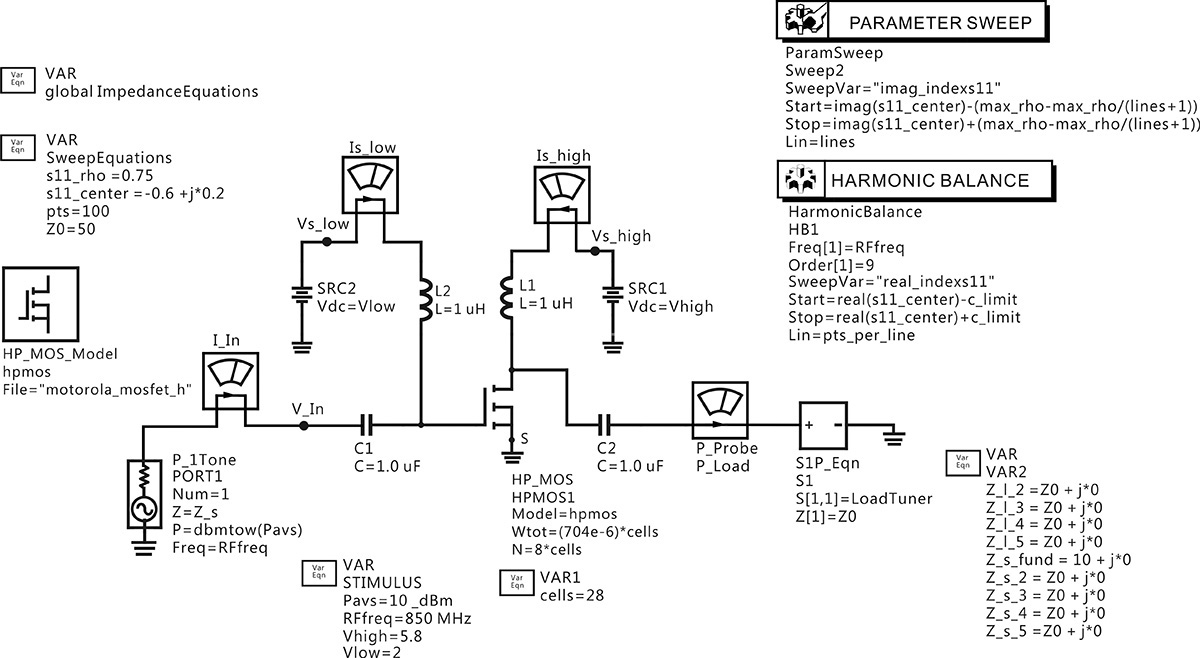
Figure 9.16 Load-pull simulation for the newly specified sample method shown in Figure 9.15(b).
The simulation for the samples in Figure 9.15(b) can be carried out by sweeping the value of Γx for a given Γy when the load reflection coefficient is defined as ΓL = Γx + jΓy. In Figure 9.16, the sweep variables real_indexs11 and imag_indexs11 are defined to represent Γx and Γy. In the simulation schematic of Figure 9.16, harmonic balance simulation sweeps the value of Γx for a given Γy in the parameter sweep. The user must specify a number of samples and a region of the circle to be sampled. This is done by entering the number of samples and the center and radius of the circle. The variable block named SweepEquations in Figure 9.16 includes the necessary variables. The variables s11_center, s11_rho, and pts represent the center, the radius, and the number of samples. Using the user-specified variables, the number of lines in the direction of the y-axis, lines, and the number of samples per line, pts_per_line, are calculated and set in the variable SweepEquations VAR, which is hidden. Measurement Expression 9.2 is an opened view of SweepEquations.
real_indexs11=0
imag_indexs11=0
Z0=50
index_s11=real_indexs11+j*imag_indexs11
s11_rho=0.75
s11_center=-0.6+j*0.2
max_rho=min(1.0-mag(s11_center),mag(s11_rho))
pts=100
lines=max(int(sqrt(pts)),1)
pts_per_line=int(pts/lines)
argument=max_rho^2-(imag(s11_center)-imag_indexs11)^2
c_limit=sqrt(if(argument<0) then 0 else argument endif)
Measurement Expression 9.2 Opened view of the variable block named SweepEquations
The first two lines in the expression are for declaring the sweep variables real_indexs11 and imag_indexs11. Note that although they are set to 0, their values are newly defined through the parameter sweep. Variable index_s11 in the next line is the definition of ΓL at the fundamental frequency using the variables real_indexs11 and imag_indexs11. The value of index_s11 is used as ΓL instead of rho in the globalImpedanceEquations shown in Measurement Expression 9.1. Variables s11_rho and s11_center were described earlier and max_rho sets the new radius using the user-specified radius. This is necessary when the center and radius settings entered by the user are out of the unit Smith chart. Thus, the newly defined max_rho replaces the user-specified s11_rho.
Next, the number of lines in the direction of the y-axis, lines, is set using the total number of sample points, pts. Since the total number of sample points is proportional to the area, the variable lines is determined from sqrt(pts). The number of points per line, pts_per_line, then becomes the total number sample points divided by the number of lines, lines. Since lines and pts_per_line must be integers, the function int(⋅) converts them all into integers. Due to such definitions, the sample points at both ends of the sample lines will be tightly spaced, while they will be widely sampled around the center line.
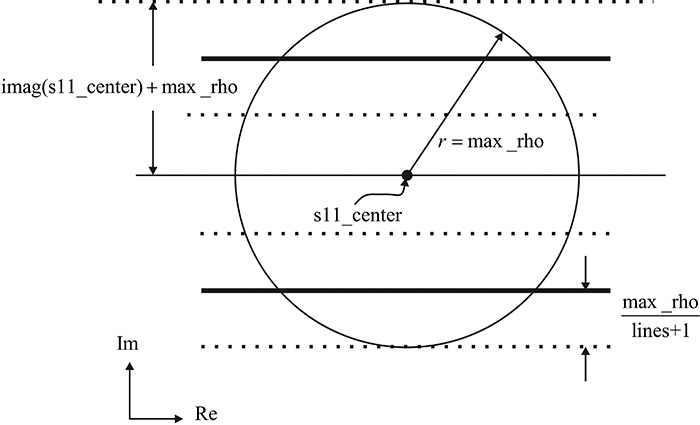
After the settings are made, in the case of the x-axis, the sweep range from the left to the right should be specified. However, the sweep range varies according to the y-axis values. That is, given y, from the equation of a circle with radius r, the possible values of x in the circle are represented by –(r2 – y2)½ ≤ x ≤ (r2 – y2)½. The value (r2 – y2)½ is represented by argument. To prevent the argument from being 0, the variable c_limit is newly defined. Therefore, the variable real_indexs11 corresponding to the x-axis reflection coefficient is swept from real(s11_center)–c_limit to real(s11_center)+c_limit, as shown in Figure 9.16. The y-axis reflection coefficient could have been swept in the range imag(s11_center)-max_rho<y<imag(s11_center)+max_rho for the number of lines. However, when lines = 2, y sweeps the two points at the end of the radius, an undesirable situation. Thus, at the end of the radius, the range is set to sweep above and below the line by a sweep range of max_rho/(lines + 1), as shown in Figure 9.17.
9.3.2.3 Display
The simulated results for the previously defined settings are the voltages and currents for the load reflection coefficient change. In order to calculate the output power and efficiency, the equations shown in Measurement Expression 9.3 are entered in the display window to calculate the DC power consumption. The index[0] in this expression represents the DC component and the exist(·) function determines whether or not the variable calculated from the simulation exists or not. The function exist(·) gives a value of 0 when the value specified by the expression does not exist. Therefore, during simulation, when the DC source and DC current probe are not defined by the names shown in Measurement Expression 9.3, the calculation results in the wrong values. The value 1e-20 is added to the DC power consumption Pdc. When the power consumption is 0, the division by zero occurs in the efficiency calculation. Then, 1e-20 is added in order to prevent division by zero without affecting the calculation results.
![]() Vs_l=exist(“real(Vs_low[0])”)
Vs_l=exist(“real(Vs_low[0])”)
![]() Vs_h=exist(“real(Vs_high[0])”)
Vs_h=exist(“real(Vs_high[0])”)
![]() Is_l=exist(“real(Is_low.i[0])”)
Is_l=exist(“real(Is_low.i[0])”)
![]() Is_h=exist(“real(Is_high.i[0])”)
Is_h=exist(“real(Is_high.i[0])”)
![]() Pdc=Is_h*Vs_h+Is_l*Vs_l+1e-20
Pdc=Is_h*Vs_h+Is_l*Vs_l+1e-20
Measurement Expression 9.3 Equations in the display window for calculating the DC power consumption
![]() Pdel_Watts=real(0.5*vload[1]*conj(Iload.i[1]))
Pdel_Watts=real(0.5*vload[1]*conj(Iload.i[1]))
![]() Pavs_Watts=10**((Pavs[0,0]-30)/10)
Pavs_Watts=10**((Pavs[0,0]-30)/10)
![]() PAE=100*(Pdel_Watts-Pavs_Watts)/Pdc
PAE=100*(Pdel_Watts-Pavs_Watts)/Pdc
![]() Pdel_dbm=10*log10(Pdel_Watts)+30
Pdel_dbm=10*log10(Pdel_Watts)+30
Measurement Expression 9.4 Equations for calculating the power delivered to the load
Measurement Expression 9.4 shows the equations for calculating the power delivered to the load and the efficiency of using DC power consumption obtained from the load-pull simulation. The first line of this expression calculates the delivered power at the fundamental frequency. However, when a power probe P_Load is used, as shown in Figure 9.16, the first line changes as shown in Measurement Expression 9.5.
![]() Pdel_Watts=P_Load.p[1]
Pdel_Watts=P_Load.p[1]
Measurement Expression 9.5 Equation for the delivered power using the power probe
The second line in Measurement Expression 9.4 calculates the input power using a variable stored in the dataset in the simulation shown in Figure 9.16. The variable Pavs becomes a two-dimensional variable because the parameter-swept simulation was carried out for two independent variables. Thus, the constant value from the two-dimensional variable Pavs is obtained by specifying Pavs as Pavs[0,0]. In addition, because Pavs is specified in dBm, the unit is changed to W by the equation in the second line. The third line calculates the PAE and the last line calculates the delivered output power in dBm. Once PAE and Pdel_dbm are calculated, they can be used to plot the contours.
![]() PAE_step=2
PAE_step=2
![]() NumPAE_lines=5
NumPAE_lines=5
![]() PAEmax=max(max(PAE))
PAEmax=max(max(PAE))
![]() PAE_contours=contour(PAE,PAEmax-0.1-[0::(NumPAE_lines-1)]*PAE_step)
PAE_contours=contour(PAE,PAEmax-0.1-[0::(NumPAE_lines-1)]*PAE_step)
Measurement Expression 9.6 Equations for drawing the contour plot
It is common practice to plot the contours from the maximum point at equally spaced step changes in a descending order. To do this, we first need to obtain the maximum value. The method for doing this is identical to that for finding the maximum of the delivered power, so only the plot of PAE contours will be discussed. Since the max(∙) function used to obtain the maximum value gives the maximum for a single sweep variable, the maximum can be obtained by using the equation max(max(PAE)) shown in Measurement Expression 9.6. The NumPAE_lines in this expression represents the number of contour plots to be drawn. The interval is set by PAE_step. Since PAE in Measurement Expression 9.4 is calculated as a percentage, this corresponds to a step of 2%. The function contour(∙) in Measurement Expression 9.6 is a function that gives the coordinates (x, y) as the output. For the coordinates (x, y), x is the independent variable of the function contour(∙) and y is the value of the function contour(∙). In addition, x is the primary sweep variable, while y is a secondary sweep variable. In the case of the example in Figure 9.16, real_indexs11 is the independent variable of the PAE_contours defined in Measurement Expression 9.6. In the case of the load-pull simulation for the polar sweep in Figure 9.13, Mag_rho is the independent variable of PAE_contours. The y coordinate value is stored in PAE_contours. Thus, to explain Measurement Expression 9.6, for example, the (x, y) coordinates can be represented as (indep(PAE_contours), PAE_contours) and the corresponding value of the contour level is stored as a separate independent variable. The obtained PAE_contours should be converted to the complex numbers in the Smith chart using the equations shown in Measurement Expression 9.7. The first two equations in that expression are used to convert the uniformly sampled swept PAE_contours into the complex numbers in the Smith chart, while the last two equations are used to convert the polar swept PAE_contour into the complex numbers in the Smith chart.
![]() PAE_contours=contour(PAE, PAEmax-0.1-[0::(NumPAE_lines-1)]*PAE_step)
PAE_contours=contour(PAE, PAEmax-0.1-[0::(NumPAE_lines-1)]*PAE_step)
![]() PAE_contours_p=[indep(PAE_contours)+j*PAE_contours]
PAE_contours_p=[indep(PAE_contours)+j*PAE_contours]
![]() PAE_contours=contour(PAE, PAEmax-0.1-[0::(NumPAE_lines-1)]*PAE_step)
PAE_contours=contour(PAE, PAEmax-0.1-[0::(NumPAE_lines-1)]*PAE_step)
![]() PAE_conts_forSmithCh=indep(PAE_contours)*exp(j*PAE_contours*pi/180)
PAE_conts_forSmithCh=indep(PAE_contours)*exp(j*PAE_contours*pi/180)
Measurement Expression 9.7 Conversion of the contour plot values into complex numbers for plotting on the Smith chart
Open the HB1Tone_LoadPull.dsn of examples/RF_board/NADC_PA_prj in ADS and modify the original simulation schematic as shown in Figure 9E.1.
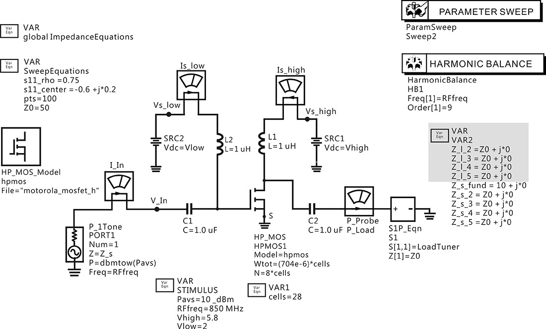
Figure 9E.1 HB1Tone_LoadPull.dsn in examples/RF_board/ NADC_PA_prj. The load impedance is swept by a uniform sample sweep. The values in the shaded area are changed from the values in Figure 9.16 for comparison.
Perform the simulation and plot the PAE and delivered power contours. Then, set the even harmonic impedance of the LoadTuner to 0 Ω and the odd harmonic impedance of the LoadTuner to 1 kΩ, and investigate the variation in the contour plot. The values of the LoadTuner can be specified using the numbers in the shaded area of Figure 9E.1.
Solution
A schematic that is different from that shown in Figure 9E.1 is displayed when the file mentioned in the specified directory is opened. After deleting the explanations in the original schematic, the schematic in Figure 9E.1 can be obtained. It can be seen that all the load impedances in Figure 9E.1 at all harmonics, except at the fundamental frequency, are set to 50 Ω. In addition, the sweep of the fundamental impedance is performed using the method shown in Figure 9.15(b). Also, the power probe P_Probe was used to calculate the power delivered to the load. Therefore, the power for the fundamental frequency becomes P_Load.p[1].
Figure 9E.2 is a comparison of the results obtained from the simulation with all harmonic load impedances set to 50 Ω (broadband load) with the simulation that has the even harmonic load impedances set to 0 and the odd harmonic impedances set to 1 kΩ (harmonic load). The comparison of contour plots for the delivered power is shown in Figure 9E.2(a) and the PAE contour plot comparison is shown in Figure 9E.2(b). It can be seen in Figure 9E.2(a) that the variations of the maximum point of the delivered power and the contours do not significantly depend on the harmonic impedance variation. On the other hand, unlike the contour plot of the delivered power, the PAE shows, to some degree, a change in response to changes in harmonic impedances. This will be explained in a later section of this chapter on class-F amplifiers. In addition, the results of the comparison are summarized as shown in Table 9E.1. The maximum powers in Table 9E.1 do not change significantly with respect to the change in the harmonic impedances but the maximum PAEs show significant changes. However, it can be seen that the fundamental impedance that gives maximum output power and maximum PAE does not change significantly.
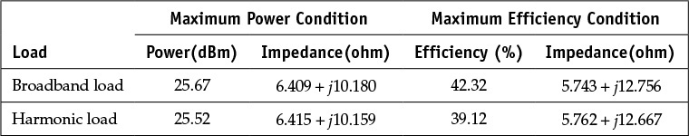
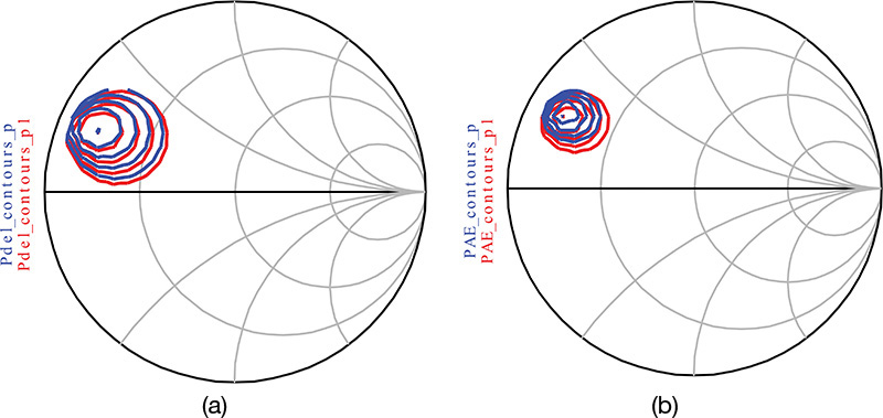
Figure 9E.2 Comparison of (a) contour plots of the output powers and (b) PAEs with broadband load and harmonic load. Pdel_contours_p and Pdel_contours_p1 are the contour plots for delivered power for broadband and harmonic loads, respectively. PAE contours are similarly drawn.
9.4 Classification
Power amplifiers are classified according to the DC bias point of the active device and the characteristics of the load network. This classification has a long history and is based on understanding the operation of the active device’s output behavior. Figure 9.18 shows the simplified IDS–VGS and IDS–VDS characteristics of an FET in order to classify the power amplifiers based on the DC bias point.
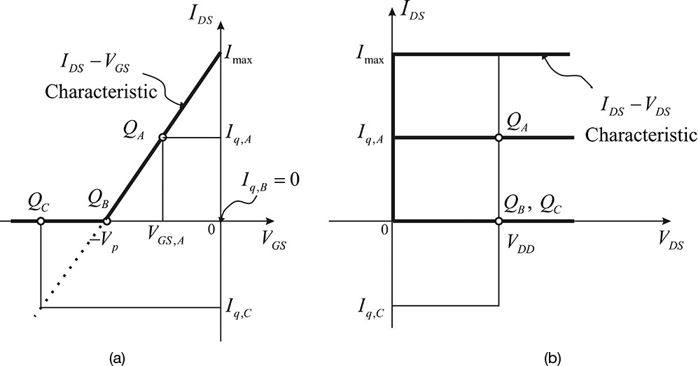
Figure 9.18 Simplified (a) IDS–VGS and (b) IDS–VDS and characteristics of an FET. Points QA, QB, and QC represent class-A, -B, and -C operating points, respectively.
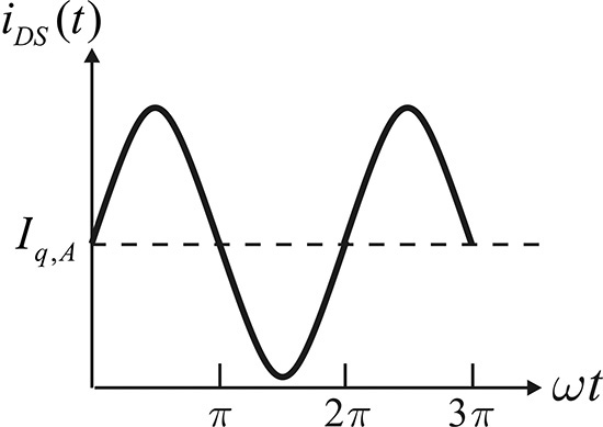
In the figure, when the amplifier is biased at VGS = VGS,A, VDS = VDD (operating point QA), considerable drain current Iq,A (quiescent drain current) flows in the amplifier even in the absence of RF input. A power amplifier that operates at this DC bias point is called a class-A power amplifier. When a sinusoidal input is applied to the class-A power amplifier, the output drain current iDS(t) conducts for a whole cycle of the sinusoidal input, as shown in Figure 9.19. Therefore, the input signal is faithfully amplified without distortion and shows a satisfactory linearity. However, as explained in section 9.1, the class-A power amplifier will have a maximum efficiency of 50%. In addition, the drain current flows even in the absence of RF input, which results in DC power consumption. Note that in the absence of RF input, the active device’s DC power consumption is maximum, which requires a large heat sink for sufficient heat dissipation.
The power consumption in the absence of RF input can be improved by moving the active device’s DC bias point. Suppose that the FET is DC biased at VDS = VDD and VGS is set at the FET’s pinch-off voltage VGS = –Vp, as shown in Figure 9.18. The DC bias point is called a class-B operating point and the power amplifier operating at this point is called a class-B power amplifier. In the class-B case, the drain current is Iq,B = 0 and will not flow in the absence of RF input. Thus, unlike the class-A amplifier, there is no DC power consumption in the absence of RF input. As another form of bias, VGS can be set smaller than the pinch-off voltage Vp of the FET. This DC bias point is called a class-C operating point and the power amplifier operating at the class-C DC bias point is called a class-C power amplifier. It should be noted that the drain current of the class-C power amplifier is also zero in the absence of RF input. On the other hand, the operating point is often mathematically interpreted as the DC bias for a negative drain current Iq,C in the absence of RF input, as shown in Figure 9.18. However, the real DC drain current is zero. The Iq,C is the projected value from the IDS–VGS characteristics curve. The drain current Iq,C at the class-C DC bias point indicates the required amplitude for the sinusoidal RF input applied to the gate to reach the pinch-off voltage. As such, the class-B and class-C power amplifiers have no DC power consumption in the absence of RF input, which is an advantage.
For a sinusoidal RF input applied to the class-B and C power amplifiers, the drain current iDS(t) flows for a conduction time interval determined according to their DC bias points, while it is zero for the remaining time interval, as shown in Figure 9.20. The time interval in which the drain current flows is called the conduction angle; the conduction angle of class-B is 180° while that of class-C is less than 180°. In addition, for an improvement in linearity and an increase in gain, a small DC current is made to flow in the absence of RF input, in which case the conduction angle becomes higher than 180°, an operation called class-AB.
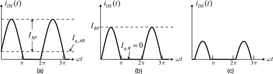
Figure 9.20 Drain-current waveforms according to an operating point; (a) class-AB, (b) class-B, and (c) class-C
As shown in Figure 9.20, the drain current waveform shows the shape of a sinusoidal tip in the conduction angle; otherwise, the RF input waveform is cut off. Distortion can naturally be expected when the RF input signal is amplified through the drain current with the sinusoidal-tip shape. Suppose that a class-B or class-C power amplifier is employed in a communication system. The amplitude and phase of the waveform in Figure 9.20 vary according to the modulated input signal. Therefore, when the RF signal is amplified by the class-B or class-C power amplifier, as shown in Figure 9.20, a loss of information may result. However, if expanded in a Fourier series, the waveform of Figure 9.20 will result in harmonics of nfo. The harmonic signals can be removed using a filter after the amplification with the sinusoidal-tip-shaped waveforms. Both the amplitude and phase of the filtered waveform at the fundamental frequency are obviously proportional to the modulated RF input because the amplitude and phase of the sinusoidal-tip-shaped waveform in Figure 9.20 is proportional to the input signal. Thus, when the IDS–VGS characteristic is linear, as shown in Figure 9.18, a relatively faithful amplified signal can be obtained. However, the transfer characteristic, such as IDS–VGS, has some nonlinearity and results in distortion. Notably, the distortion becomes more significant as the operation point moves into a deeper class-C.
Previous explanations assume that the output of the active device is considered to be a transconductance-type current source. The output resistance of the current source is ignored. In a case where the output resistance cannot be ignored, it can be included in the load network. Thus, the necessary assumption for a transconductance-type current source is that the amplitude of the input is not set sufficiently large to drive the active device into the saturation region.
In the case of the class-D and class-E power amplifiers that are introduced in this section, the active device does not operate on the basis of the transconductance-type current source. The active device in class-D and class-E operations is assumed to be a switch. That is, when the input signal is sufficiently large, the active device no longer acts as a transconductance-type current source but instead functions as a switch. The modeling of an active device as a switch becomes more appropriate when the active device is driven by a square wave. Using the square wave can significantly increase efficiency, an operation that will be explained in this section. The classification of a class-F amplifier is somewhat ambiguous. Most of these amplifiers are classified according to the load network’s characteristics.
9.4.1 Class-B and Class-C Power Amplifiers
Figure 9.21 shows class-B and class-C power amplifier configurations. In that figure, the transistor can operate in class-AB, class-B, or class-C, depending on the DC bias voltage VGS. Here, vG(t) represents the RF input signal and the drain of the FET is biased at a DC voltage VDD. Capacitor CB at the output is a DC block capacitor. Inductor L forms a parallel resonant circuit with the capacitor C at the fundamental frequency fo.
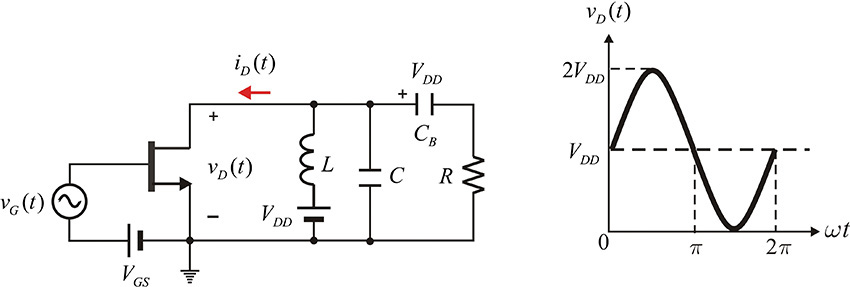
Figure 9.21 Class-B and class-C power amplifier configuration and drain-voltage waveform. The gate bias voltage VGS sets the operating point of the class-B or -C accordingly. Capacitor CB is a DC block capacitor and the parallel resonant circuit at the fundamental frequency is formed by RLC. Due to the parallel resonance, the sinusoidal waveform appears at the drain and load.
The Q = ωoCR of the parallel resonant circuit is assumed to be sufficiently large. Thus, the impedance of the parallel resonant circuit is 0 at all harmonics except at the fundamental frequency. Consequently, the voltage due to the harmonic currents is 0 and does not appear across the load resistor R. Only the sinusoidal voltage due to the fundamental current appears across R. The voltage across R is sinusoidal and the drain voltage vD(t) is thus a sinusoidal voltage waveform raised by supply voltage VDD due to the DC voltage across the DC block capacitor, as shown in Figure 9.21. Since the supply voltage VDD is fixed, by selecting an appropriate load resistor R, the maximum peak voltage can reach VDD. It must be noted that a negative voltage does not appear at the drain. When an RF input VGcos(ωt) is applied, as shown in Figure 9.22, the output waveform of the drain current can be written as

Figure 9.22 Drain-current waveform that depends on the DC bias voltage VGS. According to VGS, the drain current may have a class-B or -C sinusoidal-tip-shaped waveform.
The Iq in Equation (9.4) becomes the DC quiescent current that flows in the absence of RF input. That is, Iq = 0 when the amplifier operates in class-B and in class-C when Iq < 0. In addition, IRF is the amplitude of the fundamental drain current. Using Equation (9.4), the conduction angle θ can be determined as expressed in Equation (9.5).
Now, using θ, Equation (9.4) can be rewritten and expressed as Equation (9.6).
Thus, the maximum current is expressed in Equation (9.7).
Expanding iD(t) in a Fourier series,
iD(t) = I0 + I1 cosωt + I2 cos 2ωt + ···
where the DC current component can be obtained as shown in Equation (9.8)
and the fundamental wave component I1 and harmonic components In can be expressed as Equations (9.9a) and (9.9b),

where γ0 and γ1 are functions of the conduction angle. Thus, denoting the voltage at fundamental frequency as V1, the drain efficiency can be computed as shown in Equation (9.10).
Here, ξ is defined as
and, since V1 < VDD, generally ξ ≤ 1. Therefore, by substituting ξ = 1 and θ = ½π into Equation (9.10), the maximum efficiency of a class-B amplifier, ηB,max is expressed in Equation (9.11).
From Imax in Equation (9.7), the value of the load giving maximum output power is given by Equation (9.12).
Then, the maximum output power is expressed in Equation (9.13).
Calculate the optimum impedance Ropt of a 20-W class-B power amplifier for VDD = 20 V.
Solution
From Equation (9.13),
The meaning of the optimum load in Equation (9.12) can be understood by using a load line at the device output plane, which represents the trajectory of the voltage vD(t) and current iD(t). Using vD(t) and iD(t) in Figure 9.22, the load line can be drawn as shown in Figure 9.23. In that figure, the optimum load value that gives maximum output power in a class-B amplifier in Equation (9.12) can be easily inferred from Figure 9.23. In addition, the load resistance of a class-A amplifier that gives maximum output power is double that of the class-B amplifier. Also, from the load line of the class-C amplifier, as the conduction angle decreases, the optimum load resistance that gives maximum output power can also be seen to decrease, as shown in Figure 9.23.

Figure 9.23 Load lines of power amplifiers operating with class-A, -B, and -C. The optimum resistance is increasing as the class moves from C to A.
Set up a 1-A half-wave current source in ADS and configure the output circuit of a class-B amplifier. Set the load value from Equation (9.12) and confirm the voltage waveform vD(t) and drain efficiency. Also, plot the load line.
Solution
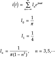
A half-wave current source can be configured in ADS using the n–tone current source, as shown in Figure 9E.3. The Fourier series of the half-wave current source,
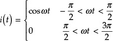
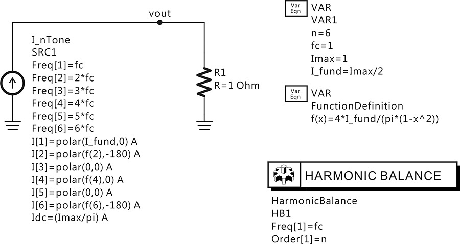
Figure 9E.3 Half-wave current source configuration. The half-wave current source is implemented using a Fourier series.
can be expressed as
It should be noted that the Fourier series uses the two-sided spectra while the phasor uses only the positive frequency, that is, the one-sided spectrum. As a result, when expressed as a phasor, and for the harmonics n ≠ 0, the doubling of the value of In is required. In addition, since harmonics are, by default, represented by phasors in ADS, the harmonic phasor is represented by doubling the coefficient of the Fourier series given in the equations above. Thus, the half-wave current source can be configured as shown in Figure 9E.3. Note that I1 (I_fund) in Figure 9E.3 represents the phasor value and is set to Imax/2. The values of the other harmonics are accordingly set using I1. The output voltage vout across 1 Ω is used to check whether the expanded harmonic current of the Fourier series correctly produces the half-wave waveform in the time domain.
After the verification of the half-wave waveform, the output circuit of the class-B power amplifier can be configured as shown in Figure 9E.4. The current source of Figure 9E.3 is employed in the circuit of Figure 9E.4. The value of Imax in Figure 9E.4 is set to 1 A and the maximum value of the half-wave current source is thus 1 A. Using the maximum current value, the value of the optimum load Ropt can be computed to be 2Vcc from Equation (9.12). Also, in order to filter out harmonics, the parallel resonant circuit must have a high Q. The Q value of the parallel resonant circuit is set to Q = 10. Using Q and Ropt, the values of the inductor and the capacitor that constitute the parallel resonant circuit can be calculated.
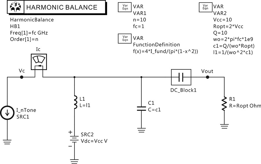
Figure 9E.4 Output circuit of a class-B power amplifier. The current source is a half-wave and L1 and C1 are resonant at the fundamental frequency. The Q value of the parallel resonant circuit is set to 10.
With the current and voltage waveforms shown in Figure 9E.5, plotting the current versus the voltage gives the load line, which is shown in Figure 9E.6. Since the voltage is not an exact sinusoidal waveform and has a slight distortion, the load line in Figure 9E.6 is not an exact straight line and shows a slight disparity.
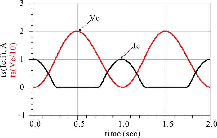
Figure 9E.5 Voltage Vc(t) and current Ic(t) waveforms. Vc(t) is almost sinusoidal while Ic(t) is a half-wave current. The function ts(⋅) generates the time-domain waveform using the set of harmonic voltages or currents.
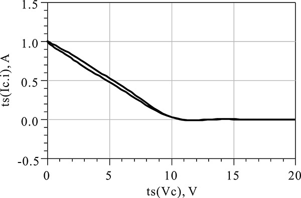
Figure 9E.6 Load line. Note that the load line is the locus of voltage Vc(t) with respect to current Ic(t).
In order to calculate the efficiency, the equations in Measurement Expression 9E.1 are entered in the display window.
![]() Vcc=10
Vcc=10
![]() Ropt=2*Vcc
Ropt=2*Vcc
![]() Idc=real(Ic.i[0])
Idc=real(Ic.i[0])
![]() eff=(mag(Vout[1]))**2/(2*Ropt)/(Vcc*Idc)*100
eff=(mag(Vout[1]))**2/(2*Ropt)/(Vcc*Idc)*100
Measurement Expression 9E.1 Equations entered in the display window to calculate the efficiency
The calculated efficiency is 78.55%, which is close to the maximum efficiency of π/4 of a class-B power amplifier.
From Equation (9.10), the maximum efficiency is obtained when ξ = 1. The maximum efficiency due to variation in the conduction angle can be expressed as Equation (9.14).
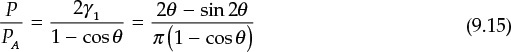
In addition, normalizing the maximum output power P, which varies with respect to the conduction angle, by the maximum power of the class-A power amplifier PA, gives Equation (9.15).
This is shown in Figure 9.24. As the conduction angle in that figure gets closer to 0, the efficiency gets closer to 100%. Also, as the conduction angle decreases, the output power decreases compared with that of the class-A power amplifier. Therefore, even though the efficiency is good, the maximum output power of the active device cannot be fully utilized. In addition, because the gain approaches 0, a significant increase in the input power is also required. Therefore, power amplifiers below class-B are not practically applicable even though they have increased efficiency.
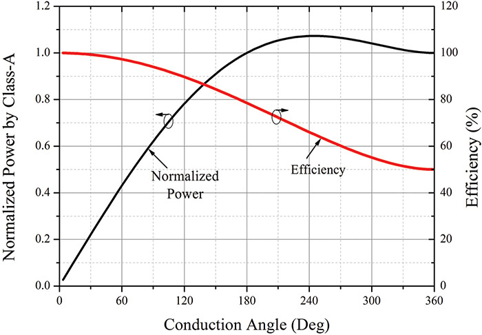
Figure 9.24 The output power and efficiency variations vs. conduction angle. As the conduction angle decreases, the efficiency increases but the output power decreases.
In the previous explanation using Figure 9.22, a class-B power amplifier is described as using a half-wave current source. It is noteworthy that a sinusoidal voltage appears across the load even though the output current of the active device shows a distorted half-wave current waveform. In addition, the phase and amplitude of the sinusoidal voltage across the load are proportional to those of the sinusoidal input. This indicates that the input signal is linearly amplified. In general, however, a class-B amplifier shows the PL–Pin characteristic shown in Figure 9.25. The PL–Pin characteristic has an S-shape for input power that causes distortion to appear in the output. This is primarily because the IDS–VGS characteristic is not linear. As a result, the PL–Pin characteristic has a distorted S-shape. This S-shaped PL–Pin characteristic can, to some extent, be corrected to a straight line by operating the amplifier in class-AB. An accurate measure of the distortion can be achieved by measuring the distortion for a modulated input signal, which will be described later in this chapter.
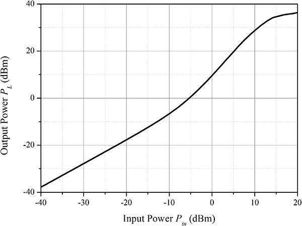
Figure 9.25 Typical output-power characteristic of a class-B amplifier for input power. Due to the nonlinearity of the ID–VGS characteristic, the S-shape curve appears.
9.4.2 Class-D Power Amplifiers
A class-A amplifier’s efficiency can be significantly improved using a class-B operation. The collector or drain efficiency of the class-B operation is, however, still under 100%. A further improvement in efficiency that is closer to 100% can be achieved by operating the active device as a switch. In the class-B power amplifier, the active device operates as a transconductance-type current source that has a sinusoidal-tip-shaped waveform. When the sinusoidal input power is further increased, the active device’s output can be modeled as a switch that turns on and off according to the input signal. As the input increases, the output of the active device is shorted in the positive half cycle, while that output is opened in the negative half cycle. Note that because the active device’s output operates as a switch, there is no DC power consumption at that output. However, delivering a large input power to the active device can lead to real problems such as damaging the active device. Therefore, applying a square-wave input instead of a larger sinusoidal input makes the active device operate more like a switch. This can be implemented by inserting a drive circuit to convert the sine wave to a square wave. The active device then operates similarly to a switch according to the input signal. This operation is called class-D. Through the class-D operation, the drain or collector efficiency can be 100%. Table 9.2 shows the difference between the two operations when the active device is operated as a switch and as a transconductance-type current source.
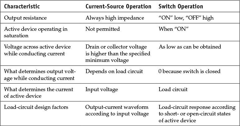
Table 9.2 Power amplifier design factors when an active device is operated as a current source or switch
An example of the class-D power amplifier circuit is shown in Figure 9.26, where inductor L operates as an RFC and allows only DC current. The DC current value is assumed to be Io. Capacitor C∞ acts as a DC block and allows only DC voltage, which is intuitively determined to be VDD. Thus, when the active device is driven into the off state by the input signal, the voltage across the drain vD is given by
vD = VDD + ILRL
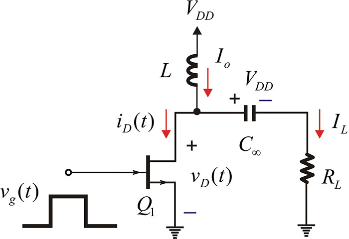
Figure 9.26 Class-D power amplifier circuit. Here, L and C∞ are an RFC and a DC block. The application of the square wave makes the transistor operate as a switch.
In addition, when the active device is on, vD is 0 and
vD = 0 = VDD + ILRL
Thus, the drain voltage alternates from 0 to VDD + ILRL according to the active device’s state, which changes from on to off. In contrast, when the active device is on, IL the current flowing through load RL is obtained as
and the drain current becomes
iD = Io – IL
Note that when the device is off, the drain current is 0, and when the device is on, the drain current has a value of Io – IL. Since the DC component must be Io, Io – IL = 2Io, then
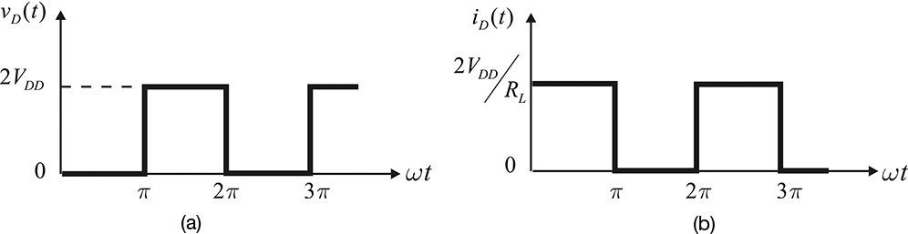
The resulting voltage and current waveforms are shown in Figure 9.27.
Using the switch provided in ADS, verify the class-D operation of the circuit in Figure 9.26.
Solution
A class-D power amplifier using the switch is as shown in Figure 9E.7. The drive signal is a square wave that varies between 1 and –1 with respect to time as the Vdc = 0 of the square-wave source. The load value is set to Ropt and the resistance of the switch for –1 V is set to 1 MΩ and for 1 V to Ropt*R_load_factor. Note that R_load_factor is set to 0.01 Ω, which is sufficiently small compared with Ropt.
Figure 9E.7 A class-D power amplifier simulation. The switch is modeled by SwitchV, which has a resistance 1 MΩ at –1 V Vsrc input and has an on-resistance of Ropt*R_load_factor at 1 V Vsrc input.
The simulated waveforms of this setup are shown in Figure 9E.8. In that figure, when the voltage is maximum, the current is 0 and vice versa. The power consumption of the DC voltage source SRC2 can be seen to be 1 W. Since the output power is 1 W, the efficiency can be seen to be 100%.
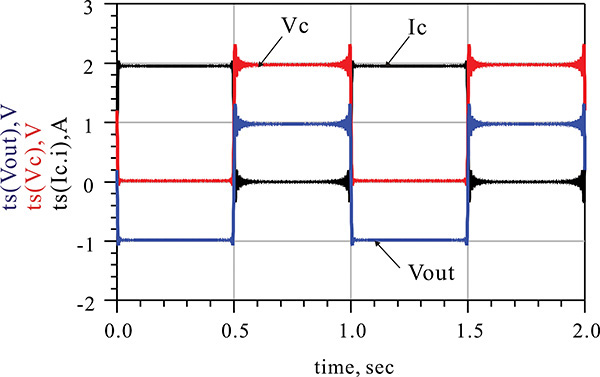
Figure 9E.8 Simulation results; (a) drain current and voltage, and (b) output voltage. Note that the average DC value of the load voltage Vout is 0. At the edge of the waveforms, ringing occurs due to Gibb’s phenomenon.
With the class-D operation, the active device’s output switches on/off according to the phase of the input signal. However, even though the phase information of the input signal is preserved at the amplifier output, the amplifier shows some losses to the amplitude information. The technique for solving this problem is that the amplitude and phase of the input voltage are separated using signal processing, and a square wave that varies according to the phase of the input signal is used as the driving input for the amplifier. The amplitude information can be restored by varying the supply voltage VDD in Figure 9.26 according to the amplitude of the input signal. Since the amplitude of the output signal of the class-D amplifier is related only to the supply voltage, the amplitude and phase information of the input signal can be restored at the amplifier output without any loss.
Even after solving the problem of the loss of the amplitude information, a significant amount of harmonics appears at the output, which presents another problem. A separate filter is required to remove the harmonics. There are several efficient ways of dealing with the harmonic problem of the class-D power amplifier. The voltage and current switching technique shown in Figure 9.28 is one of the ways to deal with the harmonic problem; see reference 3 at the end of this chapter for more information.
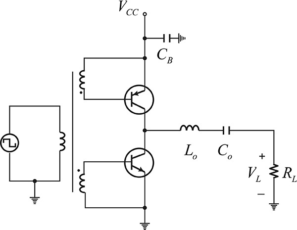
Figure 9.28 Voltage switching in a class-D power amplifier with a harmonics-eliminating filter. For high-state input, the npn transistor turns on and the current flows from the load RL to the npn transistor. For low-state input, the pnp transistor turns on the current flows from the pnp transistor to the load. The series resonant circuit eliminates the harmonics of the current and the sinusoidal voltage appears at the load.
In general, the efficiency of a practical class-D power amplifier seldom reaches 100%. One reason for the degraded efficiency is that the output voltage and current of the active device have finite rising and falling times, and a non-zero voltage appears when the device is conducting. Similarly, a non-zero current appears when the device is off. In addition, the charge on the drain capacitor, which is charged to maximum during the device’s off state, flows instantly to the drain when the device enters the on state. This sometimes causes permanent damage to the device and loss in the efficiency.
9.4.3 Class-E Power Amplifiers
The active device for a class-E amplifier, just as in a class-D amplifier, is operated as a switch. A patent for a class-E amplifier was applied for at the time when the class-E operation principle was still under development and was not yet a well-defined concept. The correct operation principle for the class-E amplifier was first analyzed by N. Sokal and A. Sokal in 1975, when they also presented its design approach.4 In addition, as there was a clear difference between the operation of the class-D and class-E amplifiers, the Sokals defined that operation as a class-E operation. The class-E power amplifier circuit developed by the Sokals is shown in Figure 9.29. However, there are various class-E amplifiers in addition to the class-E amplifier shown in that figure.
4. N. O. Sokal and A. D. Sokal, “Class E-A New Class of High-Efficiency Tuned Single-Ended Switching Power Amplifiers,” IEEE Journal of Solid-State Circuits 10, no. 3 (June 1975): 168–176.
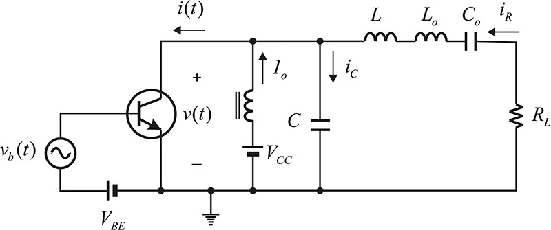
Figure 9.29 Class-E power amplifier configuration. The input vb(t) is a square wave and causes the transistor to operate as a switch. Lo and Co are resonant at the fundamental frequency. Note that the load circuit is not resonant at the fundamental frequency.
The configuration of the class-E input circuit shown in Figure 9.29 is the same as that for a class-D amplifier and the active device operates as a switch, which periodically turns on and off. Because of this, a transient analysis that depends on the on/off states is necessary to explain the class-E amplifier. Collector capacitance may exist in the collector terminal. In this case, the collector capacitance can be included in the capacitor C. DC current is supplied to the collector through the RFC, which is denoted as Io. The series resonator Lo–Co eliminates harmonics and is set to series resonate at the fundamental frequency. The Q of the series resonant branch is assumed to be sufficiently high, and harmonic currents other than those at the fundamental frequency cannot flow. Inductor L is added in series to the resonator; when the inductor is included, it makes the series resonant circuit resonate at a frequency lower than the fundamental (usually the resonator is said to be detuned). The class-E power amplifier generally has an optimized efficiency for the detuned series resonator, and it is analyzed by placing a separate L in series with the series resonator resonating at the fundamental frequency. It must be noted that the contribution of the inductor L appears only at the fundamental frequency and has no effects on the harmonics.
The output circuit of Figure 9.29 can be analyzed by considering the active device’s output as a switch. When the switch is opened, because a current Io + iR flows through capacitor C, the capacitor voltage rises and thus the collector voltage increases. On the other hand, when the switch is closed, the accumulated charge in the capacitor instantaneously flows through the switch in the form of an impulse current. In this case, even if there is a small voltage on the switch, power loss in the switch increases. This condition is not desirable for optimized efficiency. If the switch is open for the interval of 0.5T ≤ t ≤ T, the following must be satisfied at t = T for optimum efficiency, as expressed in Equation (9.16):
In addition to the impulse current due to the capacitor, a current Io + iR flows into the collector when the switch is closed. Although this is not an impulse-type current as in the case of the capacitor, it can cause a current with a step discontinuity. As this current flows instantaneously into the collector, it also leads to a loss of efficiency. In order to make this loss 0, Equation (9.17) must be satisfied.
The conditions of this equation mean that the capacitor current iC = Io + iR should be zero just before the switch is turned on. Thus, at the instant when the switch is closed, the current does not flow and the discontinuity of the current does not appear. These two conditions become the optimum conditions of the class-E power amplifier.
As a first step, the values of L and C that satisfy the optimum conditions for a given load R and supply voltage VCC should be determined through analysis. Then, the power delivered to the load PL and the DC current Io can be computed. Other parameters that must be determined include the maximum value of v(t), Vmax, and the maximum value of i(t), Imax. Using the determined Vmax and Imax, the active device appropriate for this class-E power amplifier can be selected.
Equivalent circuits based on the switch states are shown in Figure 9.30. In Figure 9.30(a), because the series resonator is assumed to have a high Q, the current through load R can be represented by iR(t) = IR sin(ωt + φ). Therefore i(t) can be expressed as
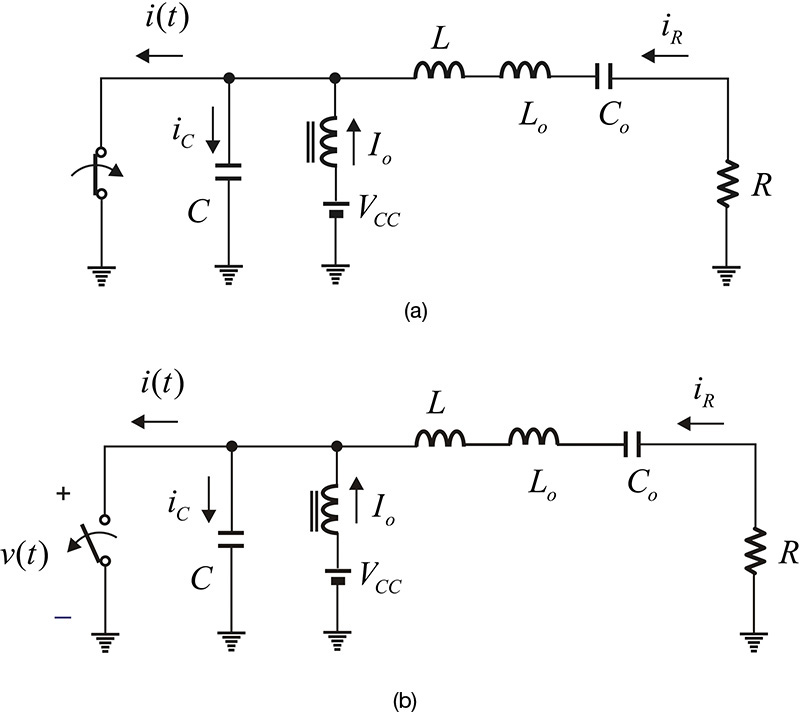
Since i(0) = 0, Equation (9.18) can be rewritten as
The current given by Equation (9.19) for the closed switch flows into the capacitor when the switch is open. Therefore, the voltage across the capacitor is obtained as shown in Equation (9.20).
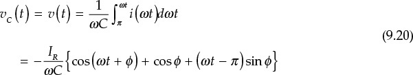

Using tan(φ) given in Equation (9.21), sinφ and cosφ can be obtained as expressed in Equation (9.22).
Then, substituting sinφ and cosφ into Equation (9.20) and rewriting, we obtain Equation (9.23).

Since the average voltage of v(t) should be VCC, the following relationship is obtained with Equation (9.24):
Therefore, normalizing v(t) by VCC, we get Equation (9.25).

In addition, normalizing i(t) by Io and rewriting Equation (9.18), we obtain Equation (9.26).
The normalized waveforms of vn(t) and in(t) are shown in Figure 9.31.
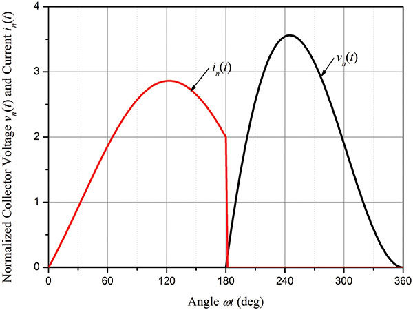
Figure 9.31 Normalized drain current and voltage waveforms. The drain voltage is continuous while the drain current shows an abrupt transition. When in ≠ 0, vn = 0, and when vn ≠ 0, in = 0. Thus, the transistor does not dissipate power and the resulting efficiency is 100%.
By differentiating Equation (9.25), the maximum voltage is obtained and expressed in Equation (9.27).
Also, by using the relationships shown in Equations (9.19b) and (9.22) where the efficiency is 100%, the power delivered to the load and DC current Io is obtained as expressed in Equations (9.28) and (9.29).
The maximum current Imax is obtained by differentiating Equation (9.26) and rewriting as Equation (9.30).
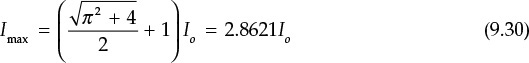
Also, applying Equations (9.19b) and (9.22) to Equation (9.28), we obtain Equation (9.31).
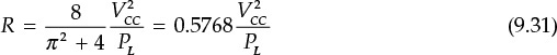
However, the values of L and C are still not determined. From the voltage in Equation (9.25), the fundamental component of the voltage is the sum of the voltage drops across the resistor R and inductor L, VR, and VL. Therefore VR and VL can be determined as
The ratio of these results is expressed in Equation (9.32).
In addition, by using Equations (9.24) and (9.29) we obtain Equation (9.33).
A class-E amplifier can be designed using the equations obtained above. Table 9.3 summarizes the formulas required for the design.
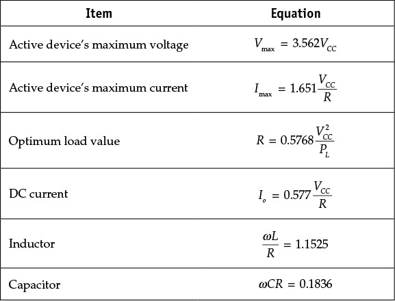
Verify the waveform of the class-E amplifier shown in Figure 9.31 by using a switch that varies according to the drive signal, and determine the load line and efficiency.
Solution
The configuration of the equivalent circuit diagram of the class-E power amplifier output is shown in Figure 9E.9. In the figure, R_load, L_main and C_main are set using the equations in Table 9.3, and the Q of the series resonant circuit is set to 20.
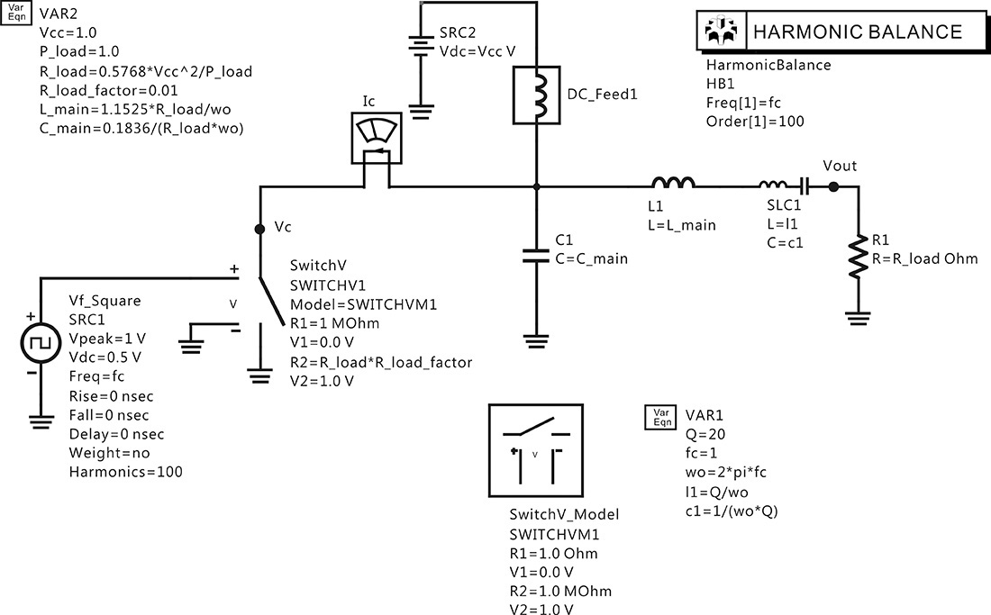
Figure 9E.9 Class-E amplifier simulation schematic. The component SLC1 is a series resonant circuit at the fundamental frequency. The value of L_main and C_main are determined using the equations in Table 9.3. The component SwitchV acts similarly to its function in the class-D power amplifier.
Simulation of the circuit in Figure 9E.9 gives the collector voltage and current shown in Figure 9E.10. It can be seen that the waveforms are the same as those calculated theoretically. Note that the voltage appearing at the load in Figure 9E.10 is close to a sinusoidal voltage, although the collector voltage and current are significantly distorted.
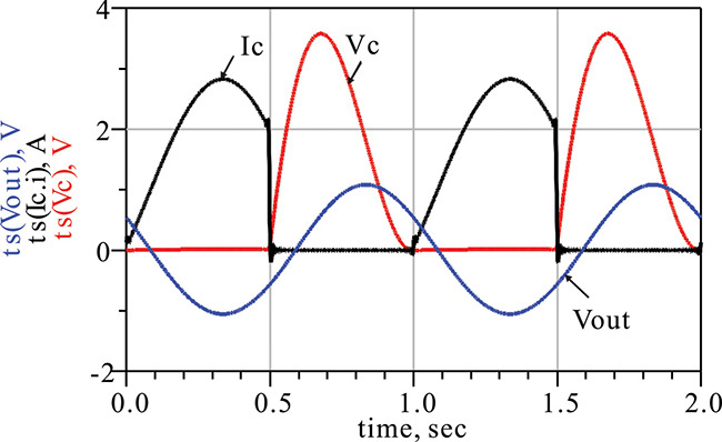
Figure 9E.10 Simulated collector voltage Vc(t), current Ic(t), and the load voltage Vout(t). Note that due to the series resonant circuit, an almost sinusoidal voltage appears at the load.
Next, the load line is shown in Figure 9E.11. The load line is considered to be the trajectory between time domain current i(t) and voltage v(t). From Figure 9E.11, the collector voltage appears when the collector current is 0 and vice versa. Thus, the active device operates as a switch and the efficiency can be seen to be 100%.
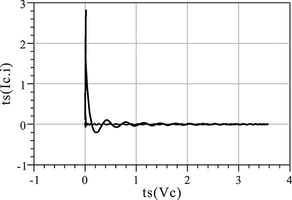
The first characteristic feature of the load circuit of the class-E amplifier is that the load circuit does not resonate at the fundamental frequency as previously explained. However, due to the series resonator in the load circuit, only sinusoidal output appears at the load. The second feature is that the current flows only when the voltage is zero, while the voltage appears only when the current is zero due to the switch operation of the active device. An amplifier with these features is a class-E amplifier and therefore the class-E amplifier is very diverse. The load circuit of the class-E amplifier explained earlier is simple and easy to implement. However, for other types of class-E load circuits that differ from that in the example, the collector voltage and current waveforms should be computed for a new optimum load circuit. The computation of the optimum load circuit becomes more complex when components such as transmission lines are used. In this case, the class-E load circuit can be approximately designed by setting the impedance of the load network at each harmonic frequency to have the same impedance as that of the class-E amplifier in Figure 9.29. For more details, refer to reference 3 at the end of this chapter.
Another feature of the class-E amplifier is that the ratio between the average and the peak values of the collector voltage or current waveform, as shown in the amplifier example, is greater than 2. Therefore, the active device used for a class-E amplifier should have a very high breakdown voltage and a maximum current. That is the disadvantage of the class-E amplifier: the active device’s maximum output capacity is not efficiently exploited.
In addition, in the calculations for the class-E amplifier, the active device was assumed to be a switch. Thus, in order to operate the active device as a switch for a class-E operation, either a driving circuit must be inserted or sufficiently high power must be applied to the input. When the input is not sufficiently high, the active device begins to operate as a half-wave current source similar to a class-B operation. Since the class-E operation is achieved when the device operates as a switch, the class-E operation is not optimum for the transconductance-type current source operation in class-B. Thus, the amplifier designed for a class-E operation does not show an optimum class-B operation. When the input drive is not appropriate, the class-E amplifier will show degradation in terms of efficiency compared to the class-B operation previously described.
9.4.4 Class-F Power Amplifiers
A class-F power amplifier is categorized by its load circuit characteristics. The load circuit is composed of multiple parallel resonators that resonate at odd harmonics in series with a class-B load circuit. The multiple parallel resonators in the output load circuit improve the efficiency of the power amplifier. Class-F power amplifiers have a longer history than do class-E amplifiers. When the parallel resonator that resonates at the third harmonic frequency is inserted in series with the load circuit of a class-B power amplifier, as shown in Figure 9.32, the collector voltage waveform can include the third harmonic frequency components. The inclusion of the third harmonic frequency makes the collector voltage waveform increasingly flat around the maximum and minimum values. A flatter waveform leads to increased efficiency.

Inserting an infinite number of odd harmonic parallel resonators in series, the collector voltage waveform becomes closer to a square wave and the efficiency becomes 100%. Instead of these multiple-harmonic resonators, Tyler presented a class-F power amplifier that uses a quarter-wavelength transmission line at the fundamental frequency, as shown in Figure 9.33. All of the amplifier’s harmonics in that figure can be ideally controlled and the class-F operation is achieved. The input drive circuit in Figure 9.33 acts as it does in a class-B power amplifier. The capacitor CB in the load side is a DC block capacitor. Inductor L1 and capacitor C1 form a parallel resonant circuit that resonates at the fundamental frequency. Thus, assuming a high Q, only the fundamental voltage appears across the load. The transmission line is one-quarter-wavelength long and the impedance seen from the collector toward the load at the fundamental frequency is (Zo)2/R. At even-order harmonics, since the transmission line becomes an integer multiple of a half wavelength, the impedance seen from the collector toward the load appears similar to that of a short circuit, while at odd-order harmonics, it appears similar to an open circuit due to the characteristic of the one-quarter-wavelength transmission line. Therefore, the one-quarter-wavelength transmission line provides a short-circuit impedance at the collector for even-order harmonics, and it provides an open-circuit impedance at odd-order harmonics. Thus, when the circuit in Figure 9.33 is compared to that shown in Figure 9.32, it acts as the infinite number of parallel resonators inserted in series to resonate at odd-order harmonics.
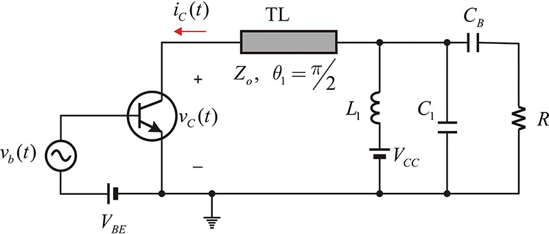
Figure 9.33 Class-F power amplifier implemented using a one-quarter-wavelength transmission line TL. L1 and C1 are parallel resonant at the fundamental frequency. CB is a DC block capacitor.
Since the impedance is an open circuit at odd harmonics, voltages of odd harmonic components can appear at the collector; however, because the impedance is a short circuit for even harmonics, voltages of even-order harmonic components cannot appear at the collector. In contrast, the opposite is the case for the current. Thus, setting θ = ωt and expressing the collector voltage and current waveforms in a Fourier series can be represented by Equations (9.34a) and (9.34b).
Figure 9.34 shows the expected collector voltage and current waveforms because, as mentioned earlier, the collector voltage waveform of a class-B power amplifier around the minimum and maximum is expected to be flattened due to the parallel resonators.
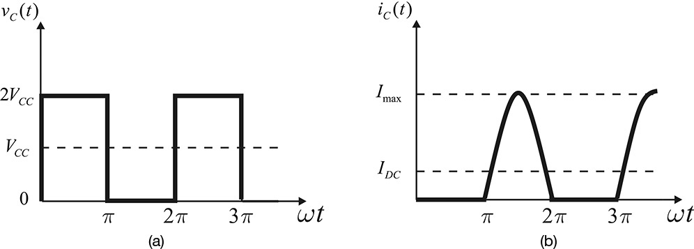
Figure 9.34 Output waveforms of a class-F power amplifier; (a) collector voltage and (b) collector current
Model the active device as a switch and obtain the collector voltage, the current waveforms, and the load voltage waveform of the class-F amplifier shown in Figure 9.33. Also, show the trajectory of the load line.
Solution
When the active device is modeled as a switch, the class-F amplifier of Figure 9.33 can be represented as shown in Figure 9E.12.
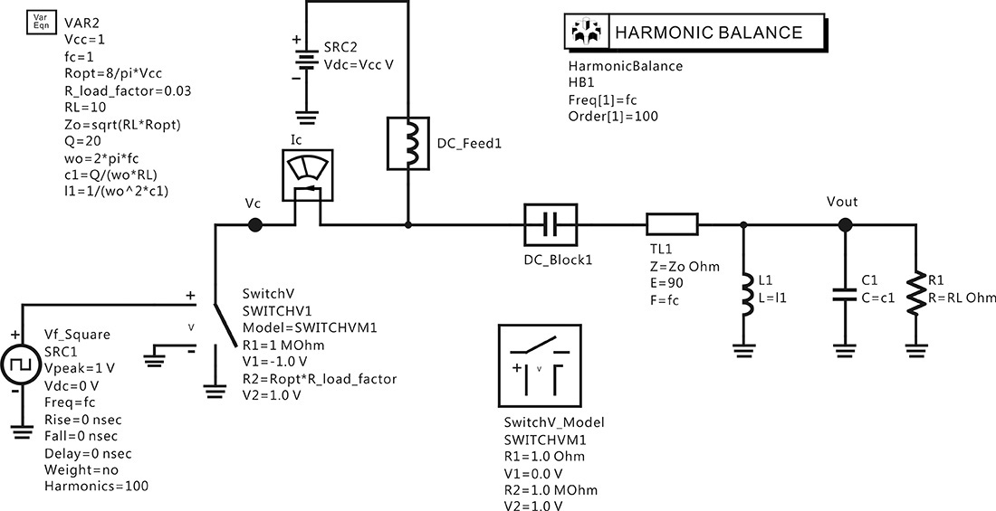
Figure 9E.12 A class-F power amplifier simulation schematic. L1 and C1 are parallel resonant at the fundamental frequency. The optimum load resistance Ropt is set to 8VCC/π. The transmission line has a quarter wavelength and its Zo is set to satisfy the relationship Ropt = Zo2/RL.
Figure 9E.13 shows the collector voltage and current waveforms, and the load voltage waveform obtained from the simulation. The collector voltage waveform in that figure can be found to approximate a square wave, while the collector current has the shape of a half wave. Some distortion in the collector voltage waveform appears as a result of the approximate switch implementation; this is due to the on-resistance of the switch. See reference 3 at the end of this chapter for more information. However, the load voltage shows an almost sinusoidal waveform due to the high Q parallel resonator connected to the load, which is set to 20. Similar to a class-E amplifier, when the voltage is not 0, the current is 0; when the current is not 0, the voltage is approximately 0 and the efficiency is close to 100%. If the on-resistance of the switch is 0, the efficiency ideally becomes 100%.
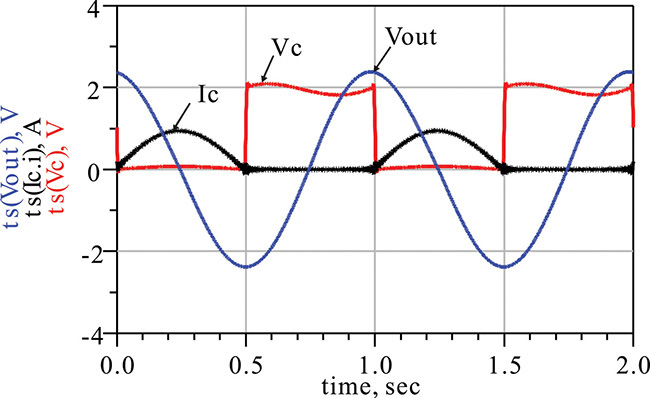
The trajectory of the load line is shown in Figure 9E.14. The load line is similar to that of class-E amplifier. However, due to the on-resistance, a slight slope occurs when the switch is on. The load line also shows distortion to some degree in the switch’s transition from off to on.
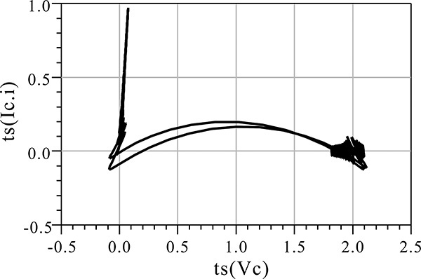
In order to design a class-F power amplifier, it is necessary to take into account the impedance of the load circuit at each harmonic. This can be determined by dividing the harmonic voltage by the corresponding harmonic current shown in Equation (9.34). Then, the load circuit of the ideal class-F power amplifier should be designed to provide the computed load impedances. The load impedance must be designed to have the optimum resistance Ropt at the fundamental frequency. For harmonics, the impedance value must be 0 at even harmonic frequencies and ∞ at odd harmonic frequencies.
An ideal class-F load circuit can be constructed using a transmission line and a parallel resonator that resonates at the fundamental frequency shown in Figure 9.33. However, because the impedance of the transmission line used to implement the class-F load circuit is generally too low, problems can arise when implementing an ideal class-F load circuit. Thus, instead of the load circuit in Figure 9.33, the class-F load circuit is generally made to satisfy the class-F load impedance condition for a limited number of harmonics, as it is generally difficult to satisfy the class-F load conditions for all harmonics. In the case of the harmonic-limited class-F load circuit, the collector voltage and current waveforms given by Equation (9.34) are reduced to those with limited harmonics. Raab has summarized the limited-harmonics waveforms and their efficiencies.5, 6 This is not a simple truncation of the Fourier series in Equation (9.34) that retains only a limited number of harmonics. The simple truncation of the Fourier series results in the well-known Gibbs phenomenon and the resulting waveform with the Gibbs phenomenon is not acceptable for the output waveform of a power amplifier. Thus, the waveform with a limited number of harmonics will differ from that obtained by truncating higher-order harmonics using Equation (9.34). Raab proposed two waveforms: maximally flat waveforms and maximum efficiency waveforms. In this section, we will review the maximum efficiency waveforms. To obtain these waveforms, the drain voltage and current are assumed not to take on negative values. To demonstrate this process, a voltage waveform example up to the third-order harmonic can be written as shown in Equation (9.35).
5. F. H. Raab, “Maximum Efficiency and Output of Class-F Power Amplifiers,” IEEE Transactions on Microwave Theory and Techniques 49, no. 6 (June 2001): 1162–1166.
6. F. H. Raab, “Class-F Power Amplifiers with Maximally Flat Waveforms,” IEEE Transactions on Microwave Theory and Techniques 45, no. 11 (November 1997): 2007–2012.
Here, the amplitude of the fundamental component has been normalized to 1. The minimum and maximum values can be obtained by taking the derivative of the equation above.
Solving Equation (9.36), we obtain Equation (9.37).
Substituting θm into Equation (9.35), the value of v(θ) at the minimum is obtained. The value should be v(θ) ≥ 0. Thus v(θm) = 0 for the maximum swing, and it results in
VCC in Equation (9.38) becomes a function of b. When the value of b is adjusted to obtain the minimum value,
From Equation (9.39), the minimum amplitude of the third harmonic is obtained. When the determined b is substituted into Equation (9.37), θm can be determined. The value of VCC then can be obtained by substituting b and θm again into Equation (9.38). Finally, the normalized amplitudes of the fundamental and third harmonic by the value of VCC can be obtained. This process can be extended to higher-order harmonics. In the case of the current waveform, using the similar calculation, the maximum efficiency waveform can be calculated from Equation (9.34) for up to the harmonic order of m–th. The results are summarized in Tables 9.4 and 9.5 where n represents the harmonic number of the voltage, while m represents the harmonic number of the current. The maximum values of voltage and current waveforms vmax and imax in Tables 9.4 and 9.5 are normalized values using the values of the DC components, and defined as shown in Equations (9.40a) and (9.40b).
In addition, the values of V1 and I1 at the fundamental frequency are also normalized using the DC values as expressed in Equations (9.41a) and (9.41b).
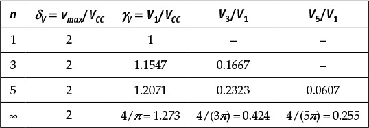
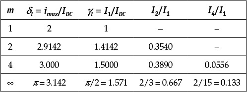
Figure 9.35 shows the voltage and current waveforms plotted using the results of Tables 9.4 and 9.5. In Figure 9.35, as the number of harmonics increases, the waveform is found to approach that of the ideal class-F power amplifier. In addition, slight ripples are observed to occur around the maximum and minimum values of the voltage in Figure 9.35. However, the ripples do not occur in the maximally flat waveforms.
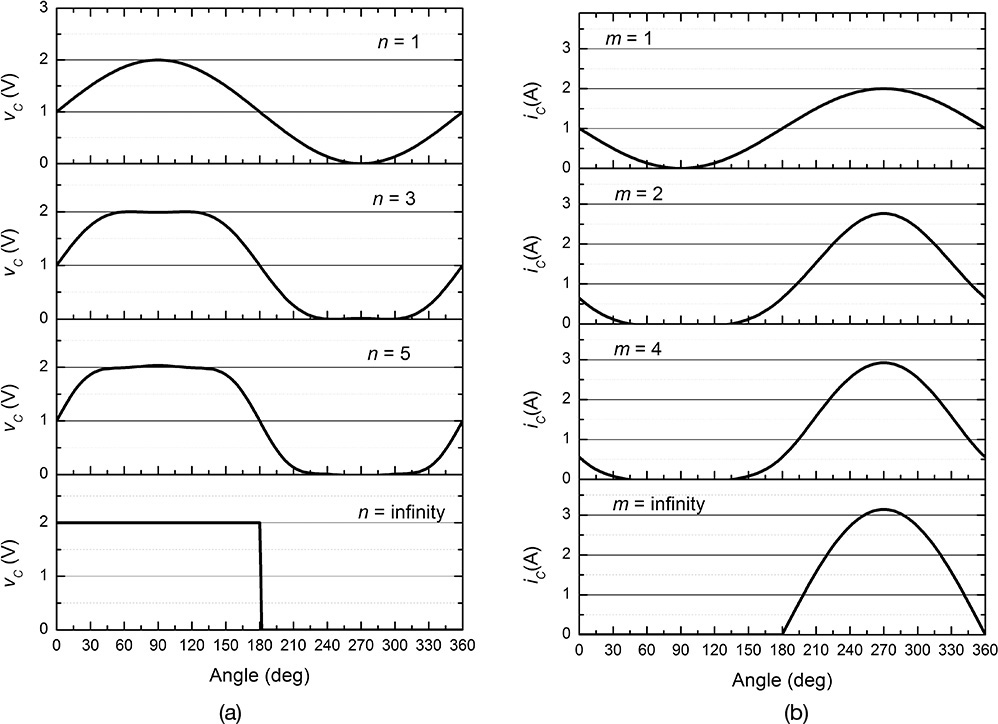
Figure 9.35 Maximum efficiency (a) voltage and (b) current waveforms of class-F power amplifier with the increase in the number of harmonics
Using the values obtained in Tables 9.4 and 9.5, the efficiency, optimum impedance, and output power capability can be calculated. First, the optimum impedance Ropt at the fundamental frequency is computed as shown in Equation (9.42).
Then, the optimum impedance of the ideal class-F amplifier Ropt at the fundamental frequency can be expressed as Equation (9.43).
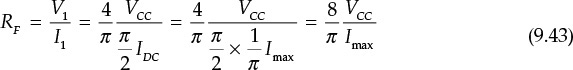
With the optimum impedance Ropt, the output power delivered to the load is shown in Equation (9.44).
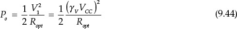
In addition, since the DC power consumption is represented by Equation (9.45),

the drain efficiency is computed as Equation (9.46).
This computation is summarized in Table 9.6.
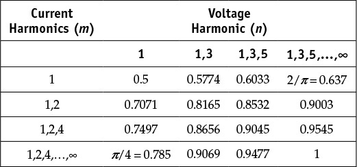
Finally, the power capability of the active device can be assessed using vmaximax. The output power of the class-F amplifier given in Equation (9.44) cannot fully utilize vmaximax, which leads to the definition of the output power capability Mp as
The output power capability given by Equation (9.47) can generally be applied to various types of power amplifiers and can be used as the criteria for assessing the effectiveness of their operations in exploiting an active device’s given output power capability. The Mp of the class-E amplifier is generally low compared to that of the class-F amplifier.
For the amplifier shown in Figure 9E.15, the supply voltage is VCC = 10 V and the maximum current is Imax = 1 A. Using Tables 9.4, 9.5, and 9.6, determine the optimum impedance Ropt, maximum output power, and efficiency.
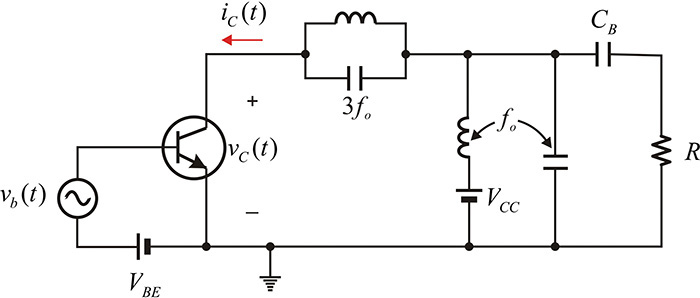
Figure 9E.15 A class-F power amplifier built from a class-B power amplifier through the third-order harmonic peaking circuit
Solution
From Figure 9E.15, the impedance seen from the collector at fo is found to be R, and at 3fo it is found to be ∞, but at other harmonics the impedance is 0. Therefore, only the voltage harmonic 1, 3 can appear at the collector. In contrast, the fundamental and all even-harmonic currents can flow toward the load, which corresponds to the case of m = 1, 2, 4, ..., and ∞. Thus, the maximum efficiency from Table 9.6 is about 90.7%. Also, in this case the ratio of the fundamental voltage to the DC voltage from Table 9.4 is
Thus, V1 = 11.55 V and, in the case of the current, since δI = π, IDC = 1/π A. Therefore, the fundamental current is
Thus,
In Example 9.7, the ideal class-F waveforms were explained by modeling the output of the active device as a switch. However, the switch model of the active device cannot explain the class-F waveforms of limited harmonics shown in Figure 9.35. The non-zero voltage appears at the time when the switch is on, and the non-zero current appears at the time when the switch is off. Thus, a reasonable model for the active device will be the transconductance-type current source model employed in the explanation of the class-B operation. The increased peak value of the sinusoidal-tip-shaped current will drive the active device output into saturation, and the clipped collector voltage appears as a result. Due to clipping, the class-F waveforms of limited harmonics can appear according to the class-F load circuit.
For the power amplifier circuit in Example 9.8, set up the output circuit of the active device as a half-wave current source. For VCC and IDC, as in Example 9.8, plot the collector voltage and current waveforms. In addition, calculate the efficiency and compare it with the previously obtained results. Also, plot the load line and discuss the problems associated with assuming a half-wave current source.
Solution
Figure 9E.16 is a schematic for the class-F load circuit with the third harmonic peaking in Example 9.8. The n-Tone source I_nTone is the half-wave current source. Here, the Q of the parallel resonant circuit at the fundamental frequency is set to 20 and that of the third harmonic is set to 30. In addition, the load impedance is set to Ropt = 23.1 Ω. The diode in the circuit is inserted to prevent the collector voltage from becoming negative. In addition, the diode ideality factor is set to 0.1 so as to be as close to an ideal diode as possible.
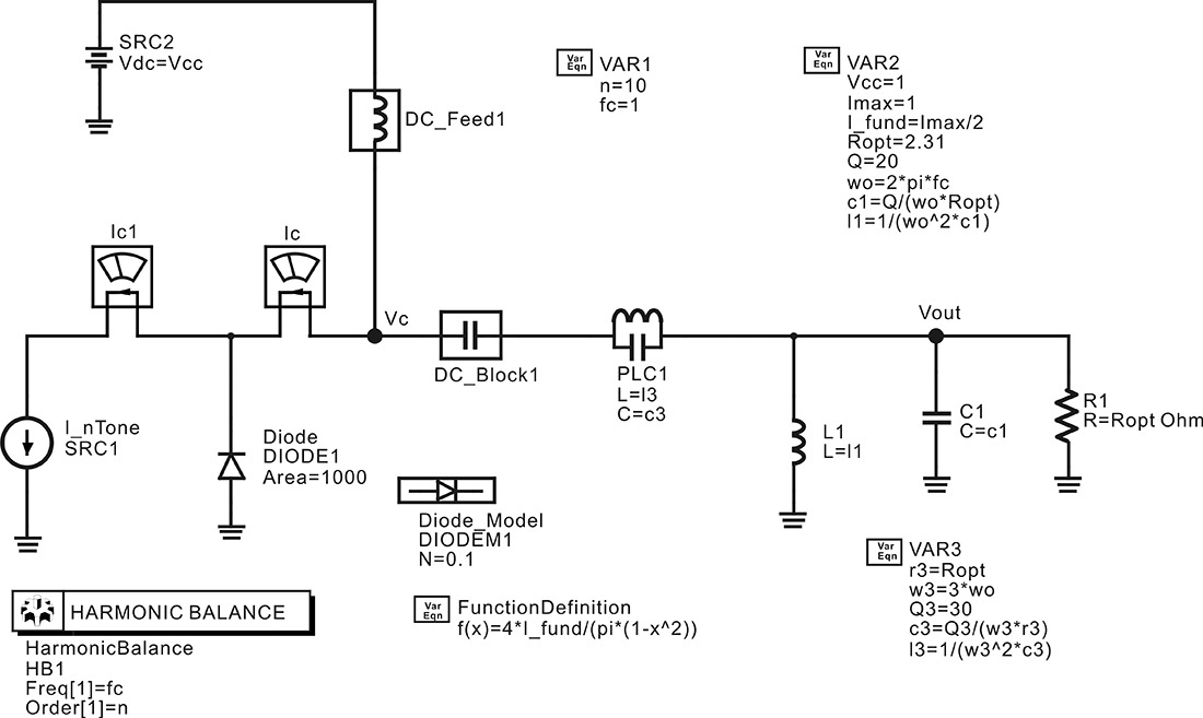
Figure 9E.16 Circuit for the simulation of the third harmonic peaking in the class-F power amplifier. SRC1 is a half-wave current source. The diode will approximately model an ideal diode and it prevents the voltage of SRC1 from being negative.
The simulated waveforms are shown in Figure 9E.17. From that figure, the collector voltage waveform around the maximum and minimum values is flattened as expected, and the collector current can also be seen to maintain a half-wave current shape. In addition, the voltage waveform across the load is shown in the figure. Although the collector voltage and current show significant distortions, the load voltage is almost close to a sine wave.
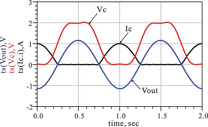
The equations shown in Measurement Expression 9E.2 are entered in the display window to calculate the collector efficiency and the delivered power to the load.
![]() Vcc=10
Vcc=10
![]() Ropt=23.1
Ropt=23.1
![]() Idc=real(Ic.i[0])
Idc=real(Ic.i[0])
![]() eff=(mag(Vout[1]))**2/(2*Ropt)/(Vcc*Idc)*100
eff=(mag(Vout[1]))**2/(2*Ropt)/(Vcc*Idc)*100
![]() PL=0.5*mag(Vout[1])**2/Ropt
PL=0.5*mag(Vout[1])**2/Ropt
Measurement Expression 9E.2 Equations for calculating the drain efficiency and output power
The calculated collector efficiency is 90.7% and the delivered power is 2.89 W. These are the same results as those calculated in Example 9.8. Figure 9E.18 shows the plot of the load line.
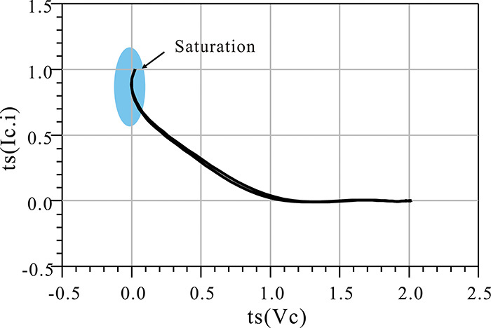
The shaded area shown in Figure 9E.18 is where the collector voltage is close to 0. In this case, it is difficult, in reality, for the half-wave current source of Figure 9E.17 to maintain the half-wave shape. As the collector voltage is close to 0, the active device is in the saturation region, and the collector current cannot maintain its half-wave shape but instead drops to zero. Therefore, the calculated collector efficiency may not be achieved. This problem is not unique to this case, and it appears for most of the class-F waveforms shown in Figure 9.35. Therefore, in reality, implementing the class-F waveform with a finite number of harmonics may lead to problems.
9.5 Design Example
In this section, we demonstrate a design example for a compact 4-W class-F power amplifier module that operates in the WiMAX frequency band of 2.3–2.7 GHz.7 The selected active device is a TGF2023-01 GaN HEMT chip device from TriQuint with a gate length and width of 0.25 μm and 1.25 mm, respectively. The shape of the active device is shown in Figure 9.36, where the source terminal of the GaN HEMT is connected to the ground at the bottom and the gate and drain terminals appear at the top. The drain supply voltage is selected as 28 V.
7. H-C Jeong, H-S Oh, and K-W Yeom, “A Miniaturized WiMAX Band 4-W Class-F GaN HEMT Power Amplifier Module,” IEEE Transactions on Microwave Theory and Techniques 59, no. 12 (December 2012): 3184–3194.
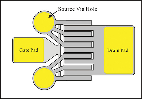
Figure 9.36 TriQuint’s GaN HEMT TGF2023-018
8. TriQuint semiconductor, TGF2023-01 6 Watt Discrete Power GaN on SiC HEMT, November 2009; available at www.triquint.com/products/p/TGF2023-2-01.
The characteristics of TGF2023-01 are shown in Table 9.7. Since the saturated output power is 38 dBm at a drain voltage of 28 V with a quiescent drain current of 125 mA, the device is considered to be adequate for the design goal of the 4 W above.
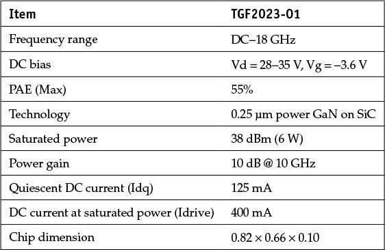
TriQuint provides the large-signal model of the TGF2023-01, which is shown in Figure 9.37. The S-parameter data components at the gate, source, and drain terminals in the large-signal equivalent circuit are those from the EM-simulated data of the source via, drain, and gate pads supplied by TriQuint. The large-signal equivalent circuit shown in Figure 9.37 is configured using the EEHEMT model whose required values are provided in the ADS discrete file format from TriQuint since the values to be entered are so many. The discrete file format consists of variable names and their corresponding values. The variable names of the discrete format file are meant to be the same as those in the EEHEMT model. The DAC (data access component) named eehemt_dac and shown in Figure 9.37 is used to read the discrete file format. Then, the variable values of eehemt_dac are read into the variable block named eehemt_vars using the expression Vto=file{eehemt_dac, “Vto”}. Now the variable values in eehemt_dac are represented by the schematic window variables that have the same name as those in the discrete format file. Only one equation of Vto is shown in eehemt_vars and other variables are hidden to avoid congestion. Then, the variables defined by eehemt_vars are again used as the input for the EEHEMT model named EEHEMTM, in which all the variables are similarly hidden except one, Vto. The extrinsic inductors and resistors appearing at the gate, drain, and source are appropriately scaled using the number of fingers and gate width. The component Scaling_Factor specifies the scaling. Table 9.8 lists the values of the EEHEMT model parameters.

Figure 9.37 Large-signal EEHEMT model of TGF2023-01.9 S-parameter data components at the gate, source, and drain are EM-simulated data for the gate, source, and drain pads. The EEHEMT model values in Table 9.8 are read into DAC eehemt_dac and those read values are again used to define the variables with the same names using the variable block named eehemt_vars. The resistances and inductances at the gate, drain, and source are separately scaled through the variable block named Scaling_Factor.
9. TriQuint Semiconductor, TriQuint EEHEMT Model Implemented in ADS and AWR for TQT 0.25 μm 3MI GaN on SiC Process 1.25 mm Discrete FET: 30 V @ 100 mA/mm @ 10 GHz, December 2009.
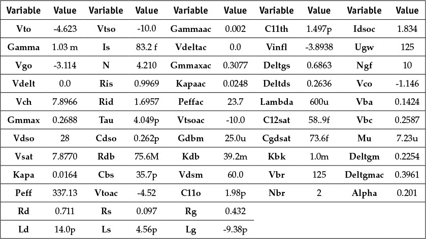
9.5.1 Optimum Input and Output Impedances
Prior to the load-pull simulation, the gate voltage giving the quiescent drain current of 125 mA at the drain voltage of 28 V in Table 9.7 is determined from a DC simulation using the large-signal equivalent circuit. The drain current versus gate voltage is plotted as shown in Figure 9.38. A DC drain current of approximately 125 mA is obtained at a gate voltage of VGS = –3.57 V.
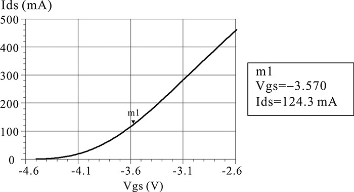
Figure 9.38 Simulated IDS–VGS characteristic at a drain voltage of 28 V. The quiescent current of 125 mA is achieved at Vgs = –3.57 V.
The gate voltage is thus determined as –3.57 V, and a drain voltage of 28 V is applied. A problem arises because the circuit is first configured to be stable before the load-pull simulation. The stability investigation requires S-parameter simulation. But before the S-parameter simulation, the S-parameters of an appropriate bonding ribbon for the connection of the active device’s gate and drain should be predetermined because they appear as fixed components in assembly. After the 3D-simulation of the bonding ribbons with a 3-mil width using AnSoft HFSS, the bonding ribbon S-parameters are determined. They appear as the S-parameter data components in Figure 9.39. The RC circuit connected in shunt to the gate is to ensure the stabilization of the active device. By adjusting the resistance value r, the stability factor can be adjusted to be greater than 1 in the full frequency band. For the value r = 55 Ω, the circuit is stabilized for a full frequency band of up to 10 GHz. Figure 9.40 shows the simulated stability and maximum gain. Since the stability factor is larger than 1 up to a frequency of 10 GHz, the device is found to be stable and the maximum gain at the center frequency of 2.5 GHz is approximately 21 dB.
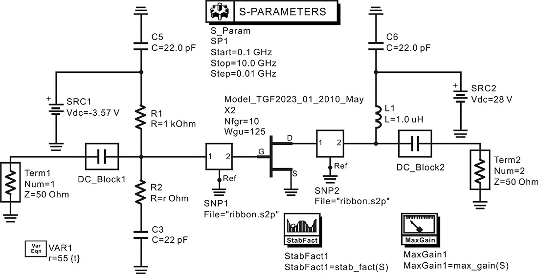
Figure 9.39 Schematic for a stability simulation. The two S-parameter components at the gate and drain represent those of bonding ribbons simulated using HFSS. The value r of resistor is tuned to stabilize the TGF2023.
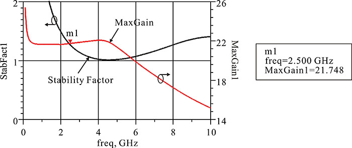
Figure 9.40 Stability simulation results at r = 55 Ω. The stability factor is above 1 up to 10 GHz and MaxGain1 at 2.5 GHz is about 21.7 dB.
After the stability circuit is thus configured, the load-pull simulation shown in Figure 9.41 is set up and the simulation is carried out to obtain the source and load impedances giving maximum output power. Here, the sweep center of the load reflection coefficient is set using the maximum output power impedance of the TGF2023-01 in the datasheet as s11_center = polar (0.32, 130°). The optimum source impedance is set to the conjugate of S11 of the small-signal S-parameters at 2.5 GHz in the datasheet. The optimum source impedance is implemented in the variable block named Initial_S11 in Figure 9.41. The circuit is thus set up and the initial load-pull simulation is carried out. Next, using the resulting initial load impedance values, the source-pull simulation is performed. This process is repeated three to four times to obtain the final results. The source impedance value that is eventually obtained is shown as z1 in the variable block named VAR4 of Figure 9.41. It must be noted that the impedance of the load in VAR2 of Figure 9.41 is set to operate in class-F up to the third harmonic. The second harmonic impedance was set to 0 and that of the third harmonic to 1 kΩ, while the rest of the harmonic impedances were set to 50 Ω. On the other hand, all the harmonic impedances of the source were set to 50 Ω. The reason for setting the source impedance is that matching at the input is performed only at the center frequency. In addition, the number of harmonics in the HB simulator is set to 3.
Figure 9.41 Load-pull simulation schematic. The available power Pavs is set to 20 dBm. The load circuit is a class-F load up to the third harmonics. The source impedance z1 is initially set to the conjugate S11. The source-pull and load-pull simulations are iterated to obtain the optimum load and source impedances.
The simulated load-pull contour plot is as shown in Figure 9.42. The maximum output power in that figure shows an output power of 37 dBm. The load reflection coefficient is 0.220∠55°, which can be seen to differ from the maximum output power reflection coefficient 0.320∠130° provided by TriQuint in the datasheet. The PAE can be seen to be approximately 60%. The difference in the maximum output power reflection coefficient is considered to be due to the addition of the stabilization circuit.

Figure 9.42 Simulated contour plots for the delivered power and PAE. The maximum output power is about 37 dBm at the load impedance of 59.587 + j22.702, which is the selected design point. The associated PAE is about 60%.
Figure 9.43 shows the source-pull simulation; see reference 1 at the end of this chapter for more information. This simulation is similar to the load-pull simulation. The load impedance value of 59.587 + j22.702 determined from the load-pull simulation is used as the load impedance, which is assigned up to the third harmonic for a class-F operation. The variable block named Impedance Equations is used to assign the sweep variable indexs11 to the source impedance. The sweep method of indexs11 is the same as the load-pull simulation, which uniformly samples the region of the circle. In addition, to supply the specified available power Pavs, the one-tone source V_1Tone is used. The value of the V_1Tone source is set using the dbmtov(·) function. Note that the impedance of the V_1Tone source is set using the impedance at the fundamental frequency Z_s_fund. The source-pull simulation results are as shown in Figure 9.44. Only the contours for the delivered power are plotted. The optimum source reflection coefficient providing the maximum delivered power can be seen to be 0.660∠132°.
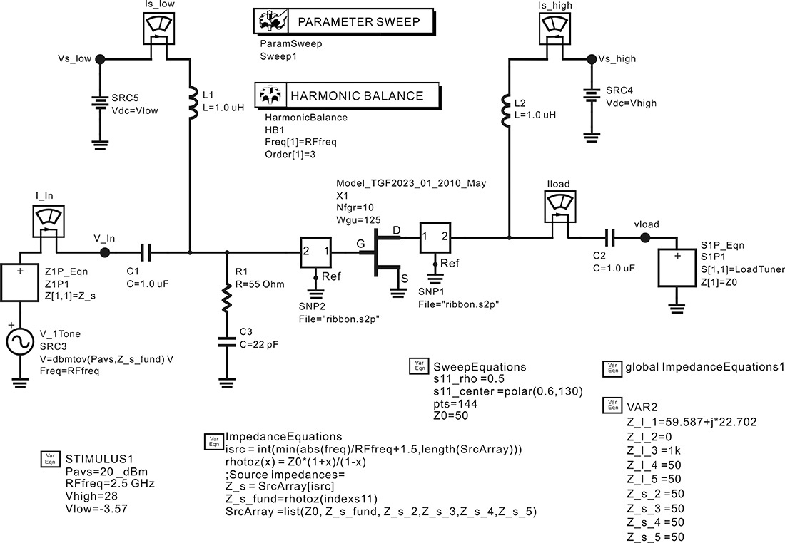
Figure 9.43 Source-pull simulation. The harmonic balance and parameter sweep are set to sweep for the source impedances, while the value of LoadTuner is fixed as 59.587 + j22.702. The source impedance has 50 Ω except at the fundamental frequency. The sweep of the source impedance is the same as the load-pull simulation and is set in the variable block named ImpedanceEquations.
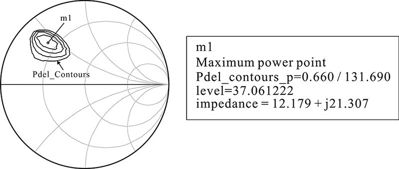
Figure 9.44 Source-pull simulation results. The maximum power is delivered at the source impedance of 12.179 + j21.307.
In summary, the simulated optimum source and load impedances are listed in Table 9.9. The output power is 37 dBm and the PAE is about 60% for the source and load impedances in Table 9.9.
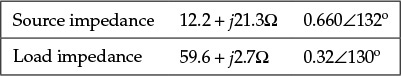
The simulation circuit shown in Figure 9.45 is set up to verify the obtained source and load impedances in Table 9.9. The source and load impedances at the fundamental frequency are declared using the variable block named VAR4 and are used to set the input and output impedance tuners. After the simulation, the equations in Measurement Expression 9.8 are entered in the display window to calculate the output power and the PAE. In addition, the equation for calculating the power gain is also entered.
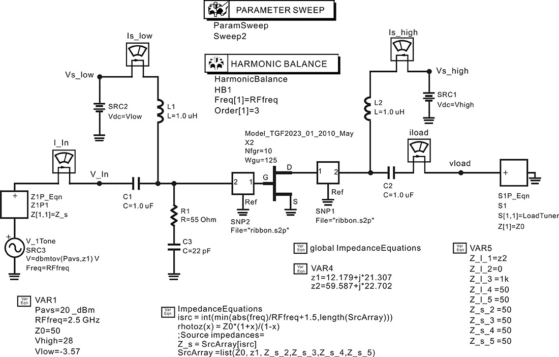
Figure 9.45 Simulation circuit for verifying the source and load impedances. These impedances obtained from the source and load pulls are in the variable block VAR4 and they are used to set the input and output impedance tuners.
![]() Pout_dbm=10*log10(0.5*real(vload[1]*conj(iload.i[1])))+30
Pout_dbm=10*log10(0.5*real(vload[1]*conj(iload.i[1])))+30
![]() Prf=10**(Pout_dbm/10-3)-10**(Pavs/10-3)
Prf=10**(Pout_dbm/10-3)-10**(Pavs/10-3)
![]() PAE=Prf/Pdc*100
PAE=Prf/Pdc*100
![]() gain=Pout_dbm-Pavs
gain=Pout_dbm-Pavs
Measurement Expression 9.8 Equation for calculating the output power, gain, and PAE
Figure 9.46 shows the calculated output power, gain, and PAE. As expected, the output power is 37 dBm at an input power of 20 dBm, and the PAE is about 62% at an output power of 37 dBm. In addition, the power gain can be seen to be approximately 20 dB.
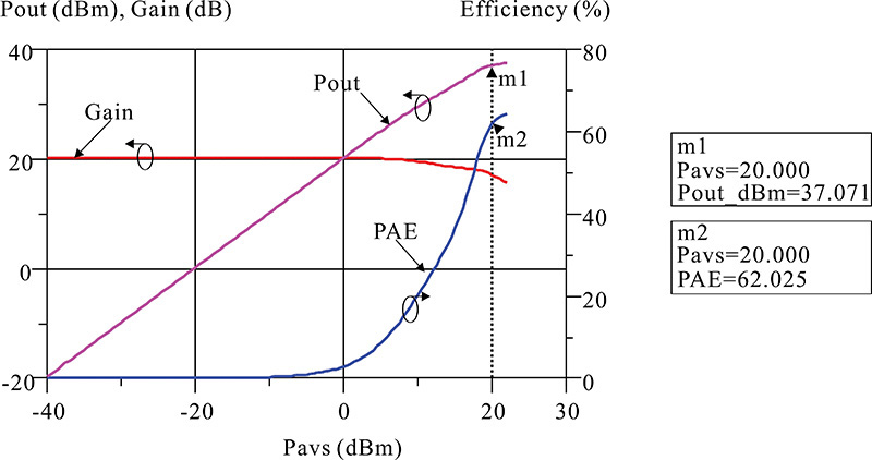
Figure 9.46 Gain, output power, and PAE for the selected impedance. The output power and PAE are about 37 dBm and 62%, respectively.
9.5.2 Input and Output Matching Circuits
A general class-F power amplifier requires an output matching circuit that yields the load impedance obtained from the load-pull simulation at the fundamental frequency and shows open for odd harmonics and short for even harmonics. However, in reality it is difficult to implement the circuit that satisfies the class-F conditions for an infinite number of harmonics. Thus, the circuit is implemented to satisfy class-F operation for a limited number of harmonics. Such circuits have been proposed by many researchers; see reference 3 at the end of this chapter for more information.
In this section, a simple implementation of the class-F output matching circuit for up to the third harmonic using lumped components will be discussed. Figure 9.47(a) shows the class-F output matching circuit that can yield the determined load impedance from the load-pull simulation. The capacitor Cp represents the drain capacitance, which is computed from the series-to-parallel conversion of the load impedance in Table 9.9. The value is fixed as Cp = 0.35 pF. In addition, GD and GL represent the drain conductance and load conductance, respectively.
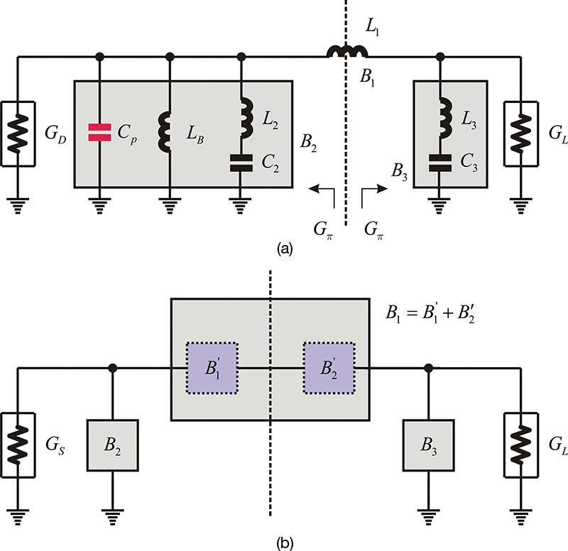
Figure 9.47 (a) Class-F output matching circuit and (b) equivalent circuit at the fundamental frequency. The matching circuit is the π-type matching circuit presented in Chapter 6.
Basically, the output matching circuit is a kind of low-pass filter that provides a short for the second harmonic frequency and an open for the third harmonic frequency. Series-connected branches L2–C2 and L3–C3 are established to be series resonant and become short at the second and third harmonic frequencies, respectively. Therefore, the circuit in Figure 9.47(a) provides a short at the second harmonic due to L2–C2, independent of the rest of the load circuit. In order for the amplifier to operate in a class-F, the impedance seen from the drain should be open at the third harmonic. Since the impedance of L3–C3 is 0 at the third harmonic, the circuit seen from the drain with the branch L3–C3 shorted should be a parallel resonant circuit. Consequently, the impedance seen from the drain terminal can be made open at the third harmonic. Thus, the circuit can be set to operate in class-F up to the third harmonic.
In addition, the circuit should have the desired load impedance at the fundamental frequency. The circuit in Figure 9.47(a) becomes a π-type matching circuit at the fundamental frequency and the equivalent circuit of Figure 9.47(a) at the fundamental frequency is shown in Figure 9.47(b). Here, the drain-side admittance at the fundamental frequency is denoted as B2, the 50-Ω load-side admittance is denoted as B3, and the series admittance is denoted as B1. Also, the ratios of the drain and load admittances to the π-matching admittance denoted as n1 and n2 are respectively defined as expressed in Equation (9.48).
Note that Gπ > GD, GL. Given Gπ, the values of B1, B2, and B3 can be calculated at the fundamental frequency ω1 following the method explained in Chapter 6 that can be expressed with Equations (9.49a)–(9.49c).
The value of B1 in Equation (9.49a) is selected to be negative because B1 is the admittance of inductor L1. From the calculated value of B1, the value of L1 can be computed as shown in Equation (9.50).
The admittance of the branch L3–C3 at the fundamental frequency is B3, which is short at the third harmonic frequency, ω3. Using the relationship (ω3)2 = (L3C3)-1,
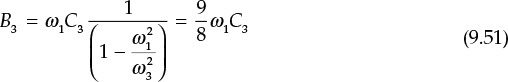
Thus, from B3, the value of capacitor C3 can be determined using Equation (9.51) and inductor L3 can be subsequently determined using (ω3)2 = (L3C3)-1. In addition, the drain-side branch admittance at the fundamental frequency is B2, and we obtain Equation (9.52).
At the same time, the admittance seen from the drain at the third harmonic frequencies is 0 and this can be expressed as
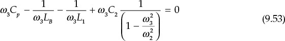
As a result, Equations (9.52) and (9.53) become simultaneous equations for C2 and LB. Thus, by solving the simultaneous equations, C2 and LB can be determined as shown in Equations (9.54) and (9.55).
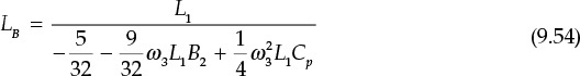
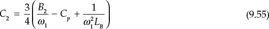
Thus, the values of all the elements in Figure 9.47(a) can be determined to satisfy the class-F operation up to the three harmonics.
The values of all the elements were calculated by setting Gπ = 2GD and using Equations (9.50)–(9.55). The calculated results give a value of LB too large to implement. Therefore, the value of Cp was increased by 0.5 pF and the values of all the elements were recalculated. Here, the increased value 0.5 pF can be implemented using a parasitic capacitor that appears together with LB. The calculated results are shown in Table 9.10.
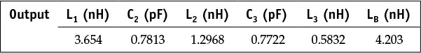
In order to verify the results above, the simulation circuit shown in Figure 9.48 is set up and the simulation is carried out. The transmission characteristic of the designed class-F load circuit is shown in Figure 9.49(a). As expected, the transmission characteristic shows a match at the fundamental frequency with the transmission zeroes at the second and third harmonics. In addition, in order to plot the impedance seen from the drain, S11, from the S-parameters renormalized by the reference, 50 Ω is plotted as shown in Figure 9.49(b). From that figure, the impedance provides an exact match at the fundamental frequency and provides a short and an open at the second and third harmonics, respectively.
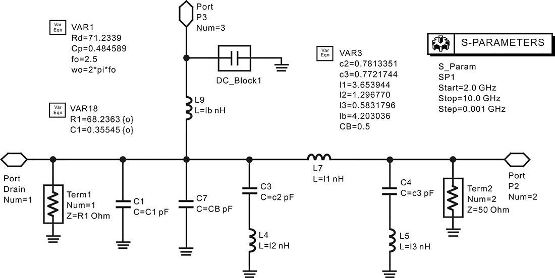
Figure 9.48 Output matching circuit simulation (CB in the figure represents the parasitic capacitor due to the RFC inductor L9, which was set to 0.5 pF)
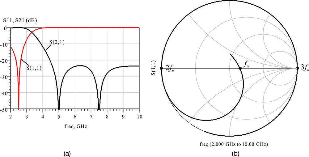
Figure 9.49 Output matching circuit simulation results; (a) transmission and reflection characteristics and (b) impedance seen from the drain. The matching is achieved at the fundamental frequency and the transmission zeroes appear at the second and third harmonic frequencies.
The input matching circuit is designed to produce the source impedance value of 12.2 + j21.3 Ω in Table 9.9. The input matching circuit can be implemented using the L-type matching circuit described in Chapter 6. Figure 9.50 is a simulation schematic for computing the element values of the L-type matching circuit through the optimization. The L-type matching circuit is a low-pass filter type. After the optimization, Ci = 2.2445 pF and Li = 2.722 nH are obtained.
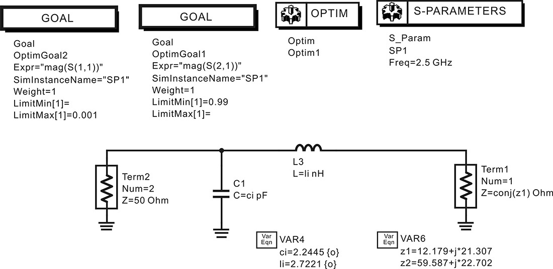
Figure 9.50 Input matching circuit simulation. The port 1 impedance is set to the conjugate of the desired input impedance and optimized for the maximum power transfer.
The entire amplifier circuit is shown in Figure 9.51. Here, the input and output matching circuits are configured as subcircuits. It should be noted that since the active device includes the drain capacitor Cp in the output matching circuit of Figure 9.48, that drain capacitor must be deactivated when the output matching circuit is configured into the output matching subcircuit. The input matching subcircuit represents the L-type matching circuit in Figure 9.50. The gate DC voltage is supplied through a 1-kΩ resistor. The input and output DC block capacitors in Figure 9.51 are set to 22 pF.
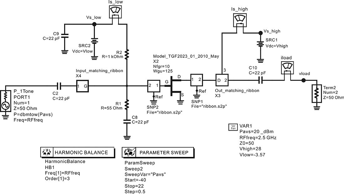
Figure 9.51 Simulation schematic for verifying the PA with the designed input and output matching circuits
The simulated output power and the PAE are shown in Figure 9.52. As in the previous simulation, the output power is 37 dBm, the PAE is about 60%, and the gain can be seen to be about 20 dB. Thus, the designed matching circuits can be seen to reproduce the characteristics obtained from the load-pull simulation results.
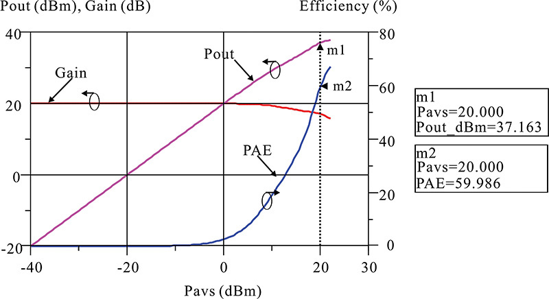
Figure 9.52 Simulated output power and PAE of the power amplifier with the lumped-element matching circuits. The small-signal gain is about 20 dB. The output power and PAE are about 37 dBm and 59%, respectively, and are exactly equal to the load-pull simulation results.
9.5.3 Design of Matching Circuits Using EM Simulation
In order to miniaturize the designed power amplifier’s size, the inductors and capacitors in the matching circuits are implemented using spiral inductors and interdigital capacitors, respectively. The selected substrate here is a 5-mil-thick alumina with a dielectric constant of 9.9. The geometrical parameters of the spiral inductor include the number of turns, the diameter, the spacing, and the line width. In the case of the spiral inductor discussed in Chapter 5, for every 0.25 increase in the number of turns, the output terminal rotates with an angle of 90° to the input. Thus, the increase in the number of turns is set to 0.25. In addition, the line width and spacing of the matching circuit’s spiral inductor are fixed at 30 mm and 10 mm, respectively. Thus, the spiral inductor value can be increased continuously by changing the diameter. In the case of the RFC inductor LB for the DC power supply, line width and spacing are fixed as 60 μm and 30 μm, respectively, in consideration of the fusing current.
Figure 9.53 shows a simulation schematic for determining the initial dimension of the spiral inductor. Using the simulation, the value of inductance can be calculated by varying the inner diameter. The determined diameters are summarized in Table 9.11. In the case of inductors L2 and L3, their values were found to be too small and so were implemented using microstrip lines.
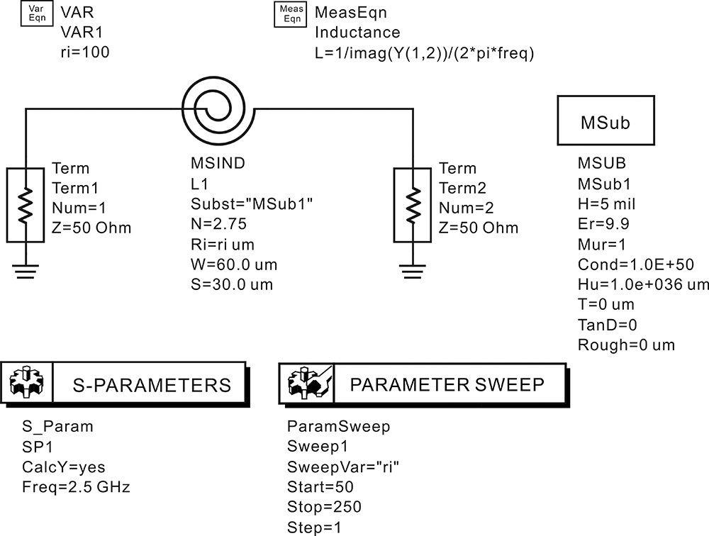
Figure 9.53 Simulation schematic for calculating the inductance of a spiral inductor. The number of turns and the width and spacing are fixed. To achieve the desired inductance, the internal diameter of the spiral inductor is adjusted.
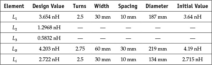
The initial dimension of the interdigital capacitor can also be configured in a similar way. The line width, spacing, length, and number of fingers of the interdigital capacitor can be adjusted; among them, only the length is varied with other parameters fixed. The continuous increase of capacitance values can be obtained by changing the length. The line width, spacing, and number of fingers are fixed at 20 μm, 10 μm, and 10, respectively, while the length is adjusted. Figure 9.54 is the simulation schematic for calculating the capacitance.
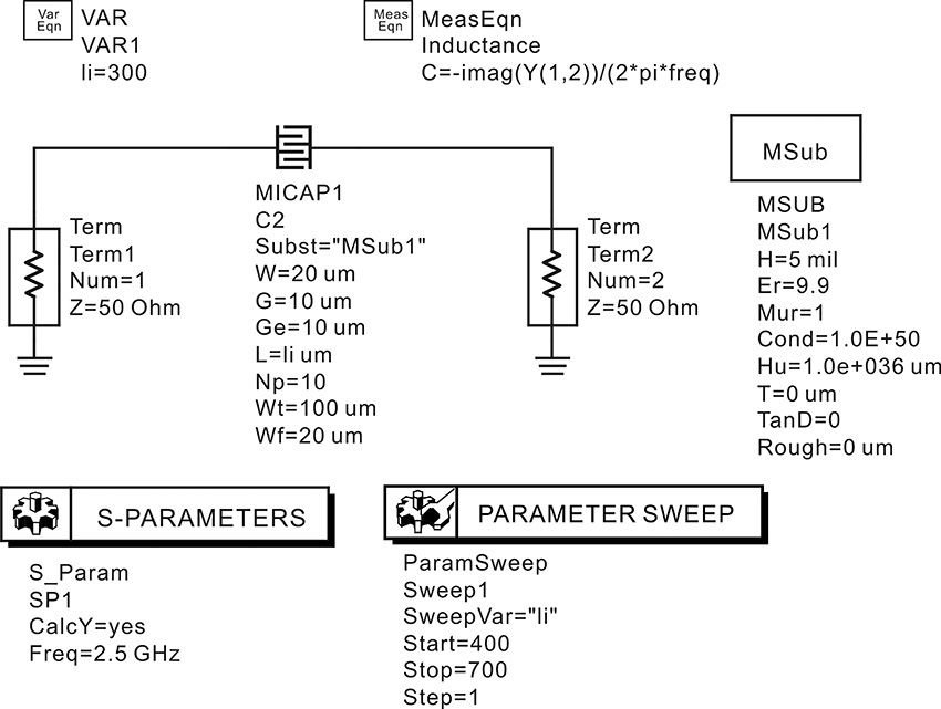
Figure 9.54 Simulation schematic for determining the initial dimensions of an interdigital capacitor. The width, spacing, and number of fingers are set to 20 μm, 10 μm, and 10, respectively. The desired capacitance is achieved by varying the length li.
The calculated dimensions are shown in Table 9.12. The value of Ci in the input matching circuit was found to be too large to be implemented as an interdigital capacitor, and so was implemented using a single layer capacitor (SLC). In addition, because the values of the DC block and bypass capacitors are also large, SLCs are used. To connect the SLC to the substrate, bonding wires are needed. The S-parameters of the bonding wire are required during simulation and have been precomputed using Ansoft’s HFSS.
Using the initial dimensions of the inductors and capacitors, an initial layout of the power amplifier can be drawn and is shown in Figure 9.55. The patterns marked 1–1’, 2–2’, 3–3’, 4–4’ in the figure are inserted for on-wafer probing of the substrate. Using the on-wafer probing patterns, the substrate can be inspected using S-parameter measurements before the assembly of the power amplifier.
Figure 9.55 Power amplifier initial layout (4.4 × 4.4 μm2). The pads 1–1’, 2–2’, 3–3’, and 4–4’ are on wafer-probe pads for inspecting the matching circuits. The substrate is a 5-mil-thick alumina with a permittivity of 9.9. The dielectric overlay has a thickness of 4 μm. The sheet resistivity is 50 Ω/square. All bonding ribbons are 3 mil.
The initial power amplifier layout shown in Figure 9.55 should be tuned using EM simulation to obtain the desired input and output impedances. Figure 9.56 shows the schematic of the co-simulation with EM simulation for the output matching circuit. The substrate in the EM simulation, as previously described, is a 5-mil-thick alumina of dielectric constant 9.9 and the conductor thickness is set to 10 μm while the conductivity is set to 4.1 × 10⁷ siemens/m. As mentioned earlier, the inductance of the bonding wire needed for connecting the DC block SLC was determined using Ansoft HFSS simulation, and the value is about 0.2 nH. The 0.2 nH inductors in Figure 9.56 represent the bonding-wire inductances. The effects of landing patterns for SLC capacitors should also be considered; in Figure 9.56, they are represented as data items that were obtained through a separate S-parameter simulation.
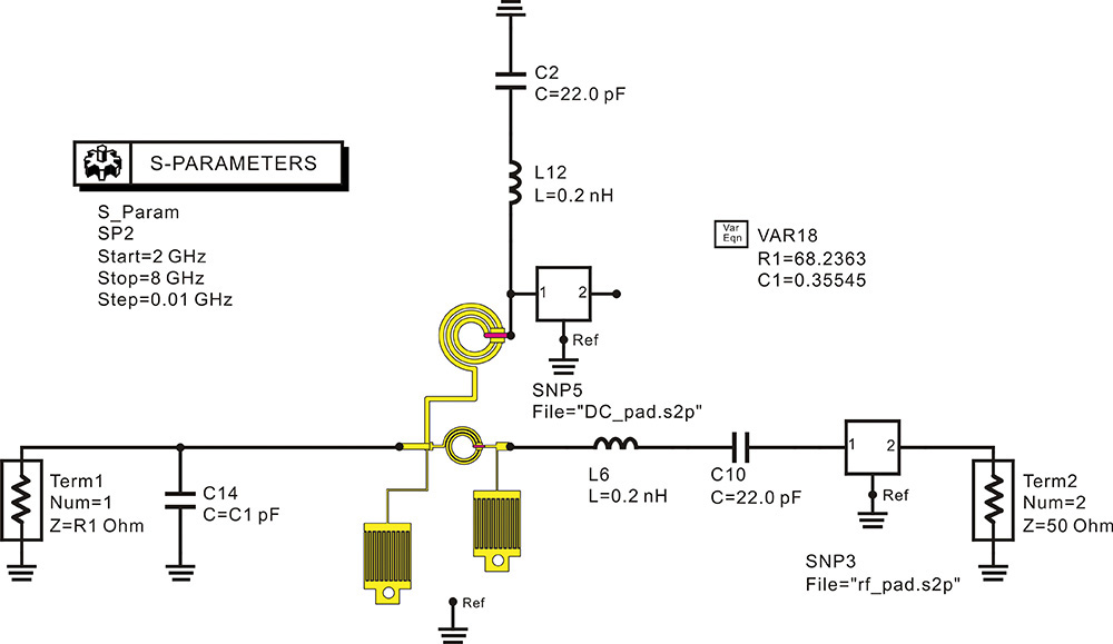
Figure 9.56 EM co-simulation of the output matching circuit. The 22-pF capacitors are SLC capacitors. The 0.2-nH inductors represent bonding-wire inductances. The C14 capacitor with a value of C1 pF is the drain capacitance. The layout component is the output matching circuit captured from the amplifier layout in Figure 9.55. To match, the inner diameters of the spiral inductors and the lengths of the interdigital capacitors are adjusted. The other dimensions are automatically adjusted according to the dimension changes of the spiral inductors and interdigital capacitors to preserve anchor points such as RF input and output, and drain bias points.
If co-simulation is not involved, the layout must be redrawn each time to reflect the changes in the layout dimensions, which is inconvenient. To work around the co-simulation, dimensions such as the inner diameter of the spiral inductors and length of the interdigital capacitors are first declared as variables in the layout. Then, those declared variables can be used as variables in the circuit simulation window. The impedance can thus be obtained from the schematic co-simulation without the necessity of separate EM simulations for the layout with the given dimensions. Using the co-simulation, the layout tuning can be carried out repeatedly until the dimensions are close to the goal.
As mentioned previously, only the inner diameter of the spiral inductor and the length of the interdigital capacitors are selected as the adjustable dimensions. Certain dimensions should be fixed even when the selected dimensions are adjusted. For example, the distance between the drain and the 50-Ω load should be fixed and should not be changed by the adjustments of the inner diameter of the spiral inductor. Also, the location of the DC supplying pad in the substrate should be fixed irrespective of the adjustments. Thus, the length of the transmission line used for connection must also be specified as a variable to prevent changes to the previously fixed dimensions in the layout. In addition, the drain capacitor is increased by 0.5 pF in the output matching circuit. The increased capacitor is implemented by the parasitic elements arising from the spiral inductor for LB and L1, and from the interdigital capacitors C2. Thus, a separate capacitor for the implementation of 0.5 pF is not used. The value of the parasitic capacitor is approximately 0.2–0.6 pF, which is somewhat dependent on the patterns of LB, L1, and C2. The output matching circuit, including the parasitic capacitor, is thus optimized in the course of the co-simulation.
The desired matching can be achieved through optimization. However, because the optimization requires significant computation time, the matching is obtained by trial-and-error adjustment in the co-simulation. The transmission characteristics shown in Figure 9.49(a) help in the adjustment technique. The second harmonic-transmission zero depends on capacitor C2 and the third harmonic-transmission zero depends on C3. Thus, the desired transmission zeroes at the second and third harmonics can be achieved by adjusting C2 and C3. The matching at the fundamental frequency can be achieved by tuning inductor L1. Thus, by adjusting capacitors C2, C3, and inductor L1, the desired output matching circuit can be achieved.
Figure 9.57 shows the EM simulation results after completing the final adjustments for the output matching circuit. As the impedance is not the 50-Ω reference impedance, the S-parameters are first converted into the 50-Ω reference S-parameters and plotted in Figure 9.57(b). In that figure, the EM-simulated impedance is found to be well-matched to the desired impedance at the fundamental frequency. In addition, the short and open impedances at the second and third harmonics, respectively, were approximately achieved. However, significant losses appear at the second and third harmonics compared to the loss results in Figure 9.49(b). Despite these losses, looking at the transmission characteristics of Figure 9.57(a), there appear to be no problems eliminating the second and third harmonics. The insertion loss at the fundamental frequency can be seen to be about 0.6 dB.
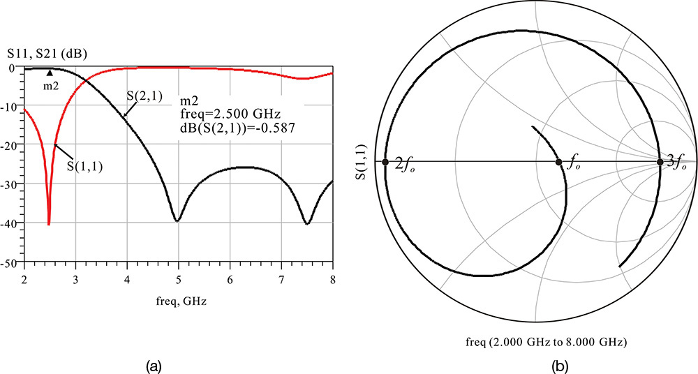
Figure 9.57 (a) Transmission characteristics of the drain to the load and (b) the EM-simulated impedance of the output matching circuit seen from the drain. The impedance seen from the drain shows a match to 68 Ω at the fundamental frequency and a short and open at the second and third harmonic frequencies, respectively. The insertion loss is about 0.6 dB at the fundamental frequency. Note that the impedances at the second and third harmonic frequencies are not exactly short or open due to the matching circuit loss.
The EM co-simulation schematic of the input matching circuit is shown in Figure 9.58. The input matching can be achieved by adjusting the value of the SLC Ci and the diameter of the spiral inductor Li. Here, the inner diameter of the spiral inductor is related to the connection of the device and input port. Thus, the length of the connected transmission line is set to compensate for the change in the inner diameter of the spiral inductor so that an assembly problem does not arise in the connection. In addition, the bonding wire of the DC block SLC at the input that cannot be simultaneously simulated in ADS Momentum is pre-simulated using Ansoft’s HFSS. This is represented by a 0.2-nH inductance, which is a fitted value that uses the HFSS simulation results. Similarly, the input-pad pattern is pre-simulated and represented by a data item for the co-simulation.
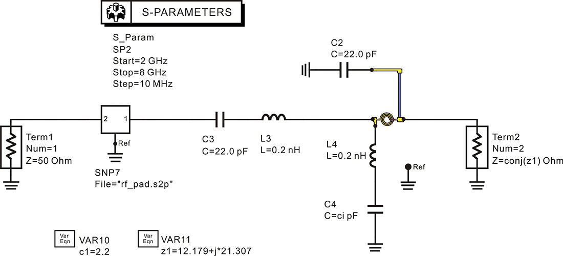
Figure 9.58 EM co-simulation schematic of the input matching circuit. C2 and C3 are SLC capacitors. The input matching is achieved by the spiral inductor and C4 with the value of ci. The inner diameter of the spiral inductor and ci are adjusted for the input impedance match. The 0.2 nH inductors represent 3-mil bonding-wire inductances. The effect of the RF pad is simulated separately and represented by the data component SNP7.
It should be noted that because the value of the capacitor Ci is not continuous, it is adjusted using fixed discrete values available from the datasheet. The calculated value is 1.9 pF. The element values of the input matching circuit can be obtained using the properties of the L-type matching circuit, as explained in Chapter 6. The value of Li is adjusted when the real part of the impedance seen from port 1 differs from 50 Ω. If the imaginary part is not matched, it is matched by adjusting the value of Ci.
The simulated impedance of the input matching circuit at port 1 is shown in Figure 9.59. In Figure 9.59(a), it can be seen that the input part is closely matched to 50 Ω at 2.5 GHz. However, looking at Figure 9.59(b), the matching circuit shows a loss of approximately 1 dB. This is considered to be caused by losses in the input matching circuit. It must be noted that although this loss is high, it does not reduce the output power. Therefore, in order to obtain the same output power, an input power greater by 1 dB must be applied to the input.

Figure 9.59 Simulated (a) S11 and (b) transmission characteristics of the input matching circuit. The input matching circuit has a loss of about –0.920 dB and transmission zero is about 6.5 GHz.
Finally, using the EM-simulated results thus obtained, the Pout–Pin characteristics of the power amplifier can be examined. The simulation schematic configured by replacing the EM simulation results by S-parameter data items is shown in Figure 9.60.
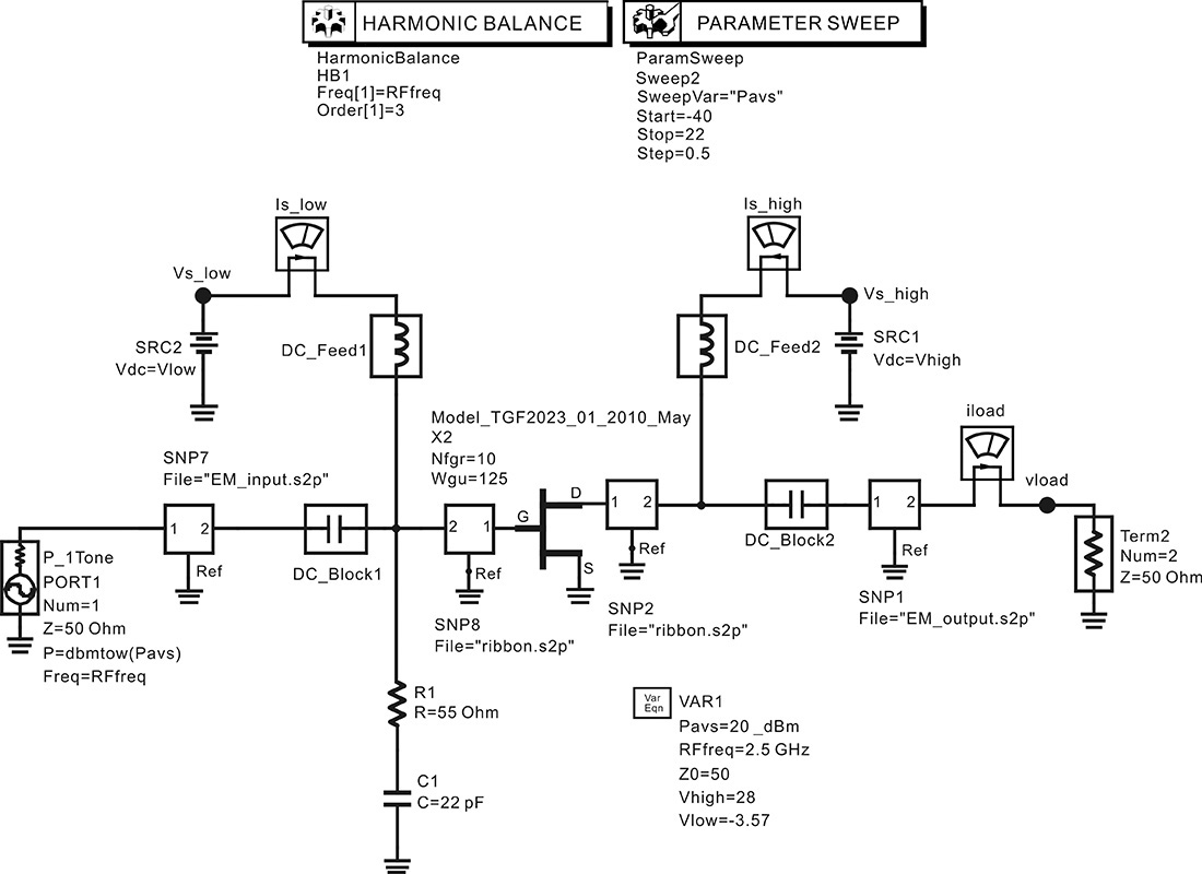
Figure 9.60 Simulation schematic for the verification of the power amplifier with the EM-simulated matching circuits. The data components SNP7 and SNP1 represent the EM-simulated S-parameters of the input and output matching circuits, respectively.
The output power, gain, and PAE are shown in Figure 9.61. Due to the losses at the input, the results at an input power of 21 dBm will correspond to the lossless circuit simulation results at an input power of 20 dBm. At 21-dBm input power, the output power is decreased by approximately 0.6 dB compared to the circuit simulation results due to the approximately 0.6-dB loss occurring in the output matching circuit. In addition, due to the same losses, the PAE is 53% and can be seen to have also decreased by about 7%.
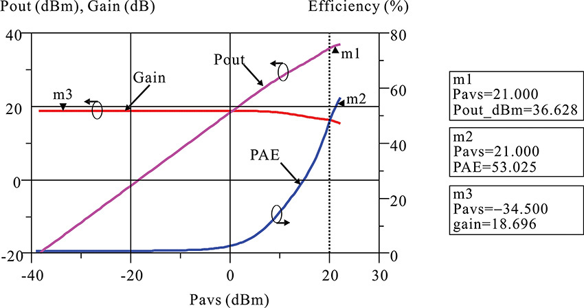
Figure 9.61 Output characteristics of the power amplifier with the EM-simulated matching circuits. The small-signal gain is reduced by about 1.5 dB compared with that of the circuit simulation due to the matching circuit loss. The input matching network has a loss of about 0.9 dB. Thus, the output power and the PAE are read at a 1-dB increased input power of 21 dBm. The output power and PAE are about 36.6 dBm and 53% at the input power of 21 dBm.
The small-signal gain characteristics obtained from the EM simulation are shown in Figure 9.62. The gain in that figure is approximately 20 dB and the return losses for both input and output can be seen to be approximately 10 dB. The reason for the poor return losses is that the power amplifier is matched at large signals. This causes a mismatch at the small-signal level and results in poor return losses.
Figure 9.62 Small-signal in-band characteristics of the EM simulated power amplifier. Because the power amplifier is matched at large signals, the input and output return losses are poor.
The transmission characteristics for the small signal are shown in Figure 9.63. As expected, the transmission zeroes can be seen to occur at the second and third harmonics. Another transmission zero exists between the two transmission zeroes as can be seen in Figure 9.63. This is the transmission zero caused by the input matching circuit, which was shown in Figure 9.59(a).
Figure 9.63 Transmission characteristic of the power amplifier with the EM-simulated matching circuits. The transmission zeroes appear at the second (about 5 GHz) and the third harmonic (7.5 GHz) due to the class-F design. The transmission zero between 6–7 GHz is due to the input matching circuit.
9.6 Power Amplifier Linearity
The previously discussed class-D, -E, and -F power amplifiers can significantly distort the input waveform, which can cause several problems in applications of power amplifiers to communication systems. The distortions in a power amplifier degrade the quality of communication, and cause problems for a receiver when demodulating a received signal. Therefore, when a power amplifier is used in a communication system, it is critical to determine whether or not the modulated input signal can be reliably demodulated beyond a certain limit. In the past, a two-tone test was the primary tool for assessing the distortion in a communication system that employed frequency division multiplexing (FDM/FDMA). In the two-tone test, a two-tone signal is applied to the input and, by measuring the amount of the third-order intermodulation distortion (IMD3), the applicability of the power amplifier can be determined. This way, the two-tone test was used as the main criterion for the applicability because the effect of intermodulation distortion on the other adjacent channels could be determined. However, with recent advances in digital communication systems, a power amplifier must transmit a digital modulation signal and the evaluation of the degree of distortion becomes a problem of significant concern.
Basically, the evaluation of a power amplifier for a digital modulation signal is, to some extent, related to the previously described two-tone test; however, the two-tone test results provide indirect evaluation for the power amplifier and a new, direct assessment method is required. This has led to the development of new test methods for assessing the degree of signal distortion in the digital modulated signal; they include the BER (bit error rate), the ACPR (adjacent channel power ratio), and the EVM (error vector magnitude) methods. These test methods are widely accepted as new standards. In this section, these methods of evaluating distortions in power amplifiers will be discussed together with simulation techniques in ADS.
9.6.1 Baseband Signal Modulation
An example of a digital bit stream is shown in Figure 9.64. The transmission rate of this signal is represented by the number of bits transmitted per unit time, and is defined as the bit rate. Its unit is bps (bit per second) and the bit rate of the signal in Figure 9.64 is expressed in Equation (9.56).
However, when the digital signal in Figure 9.64 is transmitted directly, the bandwidth required for the transmission is wider than the bandwidth given by Equation (9.56), which is 1/Tb because the waveform in Figure 9.64 contains a lot of harmonics. To avoid this situation, two transmission techniques are used. One technique uses a digital filter that removes the harmonics; the other transmits a collection of multiple bits using IQ (in-phase and quadrature-phase) modulation. Denoting the modulation carrier frequency as ωc, the IQ modulation uses two orthogonal carriers, cos(ωct) and sin(ωct) as shown in Equation (9.57).
When the odd bits shown in Figure 9.64 are assigned to I(t) and the even bits are assigned to Q(t), two bits can be transmitted simultaneously instead of only a single bit. Using the waveform in Figure 9.64 as an example, paired bits of (1, 0), (1, 1), (0, 0), ... are transmitted. A pair of bits is usually called a symbol. The number of transmitted symbols per unit time is defined as a symbol rate. In the example just explained above, two bits are transmitted as a symbol and the symbol rate can be seen to be one-half of the bit rate. Therefore, the transmission bandwidth can be reduced by half.
Extending this concept further, two odd bits can be assigned to I(t) and two even bits can be assigned to Q(t). This way, I(t) and Q(t) will each have four discrete levels. In the previous example, one bit is assigned to I(t) and Q(t), and the resulting I(t) and Q(t) will have two levels, 0 or 1. However, increasing the bit allocation to n, the levels of I(t) and Q(t) will increase to 2n. The symbol rate then is determined as
Thus, the transmission bandwidth required is reduced by 2n. In the case where one bit is assigned to I(t) and Q(t), the modulation is called QPSK (quadrature phase shift keying) or 4 QAM (quadrature amplitude modulation). The modulation is called 16 QAM in the case of 2 bits, 64 QAM in the case of 3 bits, and 256 QAM in the case of 4 bits.
When an IQ-modulated signal is demodulated, I(t) and Q(t) appear at the output. The demodulated I(t) and Q(t) can be plotted in the I–Q plane. Figure 9.65 shows the I–Q plots for QPSK and 16 QAM. This is referred to as a constellation plot. By repeatedly plotting each demodulated signal at each symbol time, all possible symbols appear at the I–Q plane and the constellation plot will be similar to the plots shown in Figure 9.65. The constellation plot can be plotted using commercially available instruments. The lower the distortions in the channel of the communication system, the more likely it is that the constellation point or symbol point will appear at a single point, as shown in Figure 9.65. However, in a significantly distorted channel, jitters of the constellation points appear, and by evaluating the jitters, the degree of distortion in a power amplifier can be evaluated.
The standard way to evaluate the jitters of the constellation points is defined as EVM (error vector magnitude) measurement. Figure 9.66 illustrates the concept of EVM measurement.
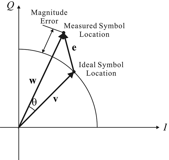
The EVM can be measured for every symbol time, as shown in Figure 9.66, and calculating the RMS (root mean square) value enables the evaluation of the degree of distortion. Thus, EVM is defined as shown in Equation (9.58).
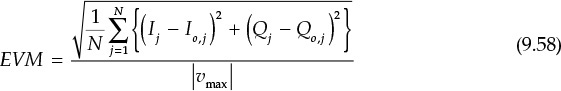
Here, Ij and Qj are the I and Q values measured at the j–th symbol time and Io,j and Qo,j are the ideal I and Q values. Also, vmax represents the value of the maximum vector magnitude of the ideal constellation point.
Figure 9.67 shows the measurement of the EVM. A spectrum analyzer with the EVM measurement utility is necessary for the EVM measurement. First, the reference constellation points are identified from the input reference signal, and then the EVM obtained with Equation (9.58) is measured by connecting the power amplifier’s output to the spectrum analyzer.
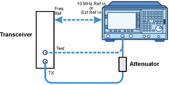
Figure 9.67 EVM measurement.10 The test signal is measured first and becomes the reference of the constellation plot. Then, the power amplifier’s signal is connected to the spectrum analyzer, which then evaluates the EVM with the built-in utility.
10. Agilent Technologies, Inc., Agilent Technologies ESA-E Series Spectrum Analyzers Modulation Analysis Measurement Personality, E4402-90071, 2002.
We have discussed that the required transmission bandwidth can be reduced using the IQ modulation. Another method to reduce the bandwidth is to use a low-pass filter, which converts the harmonic-rich bit waveform shown in Figure 9.64 into a smooth waveform. However, a simple analog lowpass filter generates ISI (intersymbol interference). When the bit waveform in Figure 9.64 is viewed as a superposition of independent square waveform bits, the analog low-pass filter’s output waveform for a bit overlaps with that of another bit, which causes problems in the decision of bits. Usually, the impulse response waveform of an analog low-pass filter disappears at t = ∞. Thus, the response of each bit overlaps, which results in an error in bit value at the sample time or the decision time, denoted as • in Figure 9.64.
Thus, a filter giving the impulse response
h(nTb) = 0 n ≠ 0
is required. As an example, the following impulse-response waveform in Equation (9.59) gives a value of 0 at t = nTb and it does not affect other adjacent bits.

The spectrum of this impulse response H(f) is given by Equation (9.60) and is called a raised-cosine filter. The α here is called the roll-off factor; its value is selected between 0 < α < 1, and 0.5 is usually used.
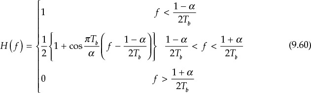
Figure 9.68 shows the plots of h(t) and its frequency response H(f) given by Equations (9.59) and (9.60). In that figure, when a digital-bit waveform is passed through a raised-cosine filter, the bandwidth of the transmitted signal is determined as approximately 1/Tb.
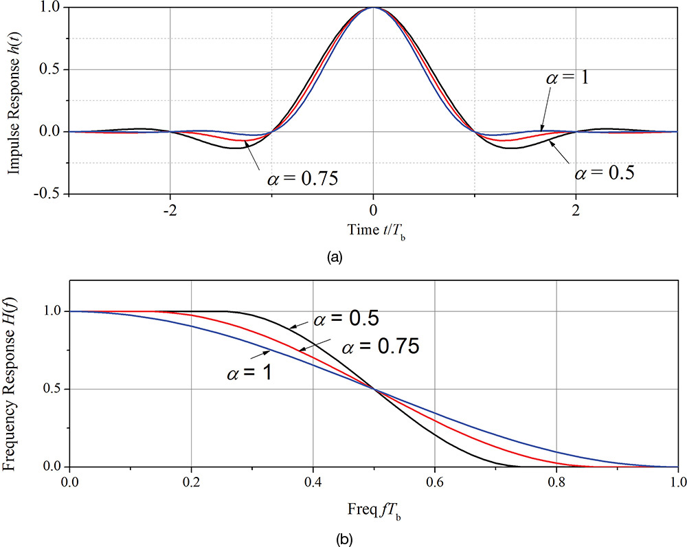
Figure 9.68 Raised-cosine digital filter: (a) impulse response, and (b) frequency response. Note that h(t) is zero for t = nTb. The bandwidth of the low-pass raised-cosine filter is about 1/(2Tb).
9.6.2 Envelope Simulation
Most digital modulated signals in digital communication systems can be expressed as shown in Equation (9.61).
The complex amplitude or phasor A(t) is called an envelope and is assumed to be a slowly varying waveform compared to the carrier, while signal x(t) can be viewed as a sine wave with the time-varying envelope as its amplitude. An example of the waveforms is shown in Figure 9.69.
Figure 9.69 Example of a modulated signal in the time domain. The signal can be represented by the product of the time-varying envelope and carrier.
Figure 9.70 shows this signal behavior in the frequency domain. Here, the sine-wave envelope signal is chosen. The signal can be considered as a sine wave having amplitude A1 at time t1; the spectrum for the signal at time t1 appears on the right side of Figure 9.70. Similarly, at time t2, the signal can be considered as a sine wave having amplitude A2. Thus, the modulated digital signal given by Equation (9.61) can be seen as a carrier whose amplitude is slowly varying with time in the frequency domain.
Figure 9.70 Spectrum of an amplitude-modulated waveform in the frequency domain. The carrier power in the frequency domain slowly varies with time.
Figure 9.71 shows the concept of the approximate circuit analysis for the envelope-modulated input signal. First, harmonic balance simulation is performed for the input sine wave with constant amplitude V(t1) at sample time t1. The resulting output can be represented by harmonics and the amplitude of the fundamental frequency becomes A(t1), as shown in Figure 9.71. Here, A(t1) is called the envelope for the fundamental carrier and other envelopes for other harmonics can be similarly defined. The amplitude A(t1) is the approximate envelope of the time-varying output signal that corresponds to the time-varying input envelope signal. Through sequential harmonic balance simulations (also called envelope simulation), the envelope of each harmonic is obtained from the simulation results. Thus, the time-domain waveform of the envelope can be observed. Note that the envelope can be interpreted as a time-varying phasor. Furthermore, by expanding the envelope waveform in a Fourier series, the spectrum of each envelope can be seen in the frequency domain. Envelope simulation is used for analyses such as determining the ACPR of a power amplifier, the transient response of an oscillator, the tracking response of a PLL (phase locked loop), and so on. The details of the envelope simulations can be found in the ADS manual.
Figure 9.71 Envelope simulation concepts. The spectrum of the time-varying envelope can be obtained through FFT.
Open the QAM_16 in the ADS examples/Tutorial/ModSources_prj directory and plot the I(t) and Q(t) waveforms. Also, plot the waveform after it passes through the raised-cosine filter. In addition, plot the constellation as well as the spectrum of the modulated waveform. Finally, plot the probability distribution of the time-varying output power of the modulated signal.
Solution
Figure 9E.19 shows the opened view of the QAM_16 file.
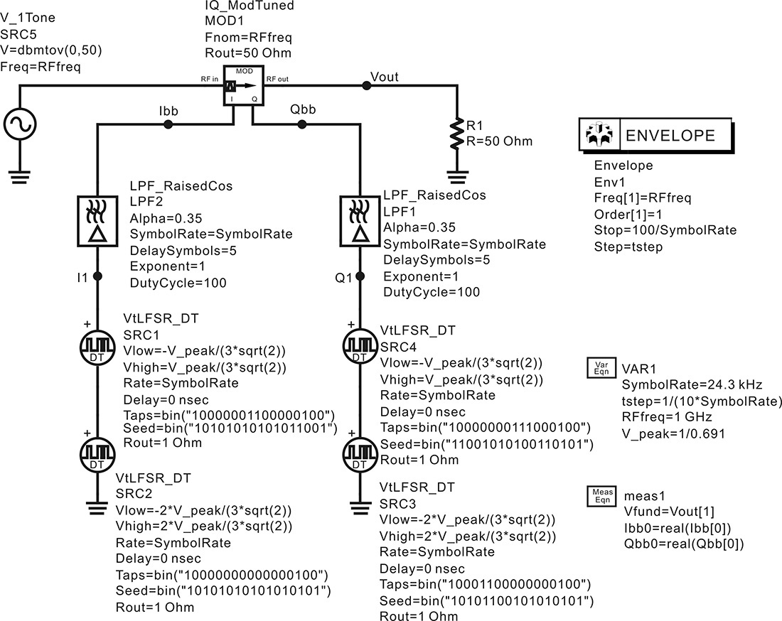
Figure 9E.19 A 16-QAM signal generation. The baseband sources SRC1, SRC2, SRC3, and SRC4 generate random bipolar digital signals. SRC1 and SRC4 are for LSB while SRC2 and SRC3 are for MSB. The two-sum digital signals in the I and Q channels are filtered by the low-pass raised-cosine filter with a bandwidth of the symbol rate. The IQ modulator MOD1 modulates the filtered digital signals using RF carrier V_1Tone of power 0 dBm. Actually, the IQ digital signals should be generated by serial-to-parallel data conversion and DAC; however, for simplicity in simulation, they are generated by the sum of the MSB and LSB digital signals. Although the power of the RF carrier is set to 0 dBm, the average modulated power is not 0 dBm. To make the power level 0 dBm, the digital signal amplitude V_peak is adjusted for 0 dBm average power.
In practice, the baseband I(t) and Q(t) signals for a 16 QAM signal is obtained by serial-to-parallel data conversion followed by digital-to-analog conversion. For a serial digital-bit stream input, two serial bits are paired into a two-bit parallel data by a serial-to-parallel data converter. Through the serial-to-parallel data conversion, a pair of two-bit parallel data corresponding to the I(t) and Q(t) signals can be generated. Each of the two-bit parallel data are then converted to an analog signal through a digital-to-analog converter (DAC). However, baseband I(t) and Q(t) signals are directly generated by removing the serial-to-parallel converters and the DACs in QAM_16 in Figure 9E.19. The values of MSB (most significant bit) and LSB (least significant bit) are specified as
The factor 3(2)½ is for normalization. When the maximum vector magnitude of the constellation is set to 1, the projection of the MSB onto the I-axis has a magnitude of 1/3(2)½. Therefore, I1 in Figure 9E.19 represents the sum of the two signals that correspond to the MSB and LSB. The Q(t) signal Q1 is similarly constructed. As the MSB and LSB signals must have random distributions, a digital feedback method called Tap and Seed is used to generate a random distribution.
The reason for setting the variable V_peak is to set the average power of the IQ-modulated signal to 1. Since the modulated signal x(t) from Equation (9.57) can be expressed as Equation (9.62),
the power of signal x(t) is proportional to (I(t) + Q(t))½. The power varies according to the random IQ modulation signals. The average power of an IQ-modulated signal must be set to 1. The value of V_peak is set to 1/0.691 for this purpose. The value of V_peak must be readjusted when a different random signal, say PRBS (pseudo-random binary sequence), is employed.
The generated baseband IQ signals pass through the raised-cosine digital filters and are converted into smooth waveforms in the time domain. Here, the exponent of the raised-cosine filter is 1 and the roll-off factor is set at 0.35, giving a 0.35 roll-off factor raised-cosine filter. Next, both smoothed I(t) and Q(t) signals are applied to the modulation inputs of an IQ modulator. The RF input signal is a sinusoidal voltage source. The source voltage corresponding to a power of 0 dBm under a 50-Ω load condition is set using the function dbmtov(·). The symbol rate in the variable block named VAR1 is set to 24.3 kHz, which is equal to the symbol rate of the raised-cosine filter.
The envelope simulation setting is similar to the transient simulation setting. The time step tstep is set to 10 times the symbol rate. Stop time is set to 100/SymbolRate, which corresponds to 100 symbols. The voltages defined as Ibb and Qbb are the filtered baseband signal, and a Measurement Expression is used to view Ibb and Qbb at the output. In the case of HB simulation, since baseband signals correspond to DC signals, the outputs are obtained by setting real(Ibb[0]) and real(Qbb[0]). Figure 9E.20 shows the waveform before and after it passes through the raised-cosine filter. In Figure 9E.20, the waveform after passing through the filter is delayed by 5 symbols and it has become considerably distorted compared to the input waveform. However, the values at a sample time, which are marked as •, have not been affected.
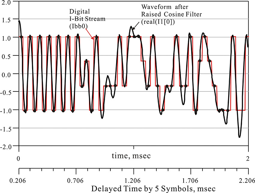
Figure 9E.20 Waveforms before and after passing through the raised-cosine filter (RCF). Although the RCF-filtered waveform is significantly distorted, it has exactly same value as the I(t) at the sample time. The RCF-filtered waveform is drawn along the bottom time axis and is delayed by 5 symbols, 2.056 msec.
To draw the constellations, the equations shown in Measurement Expression 9E.3 are entered in the display window. The Rotation here is entered to rotate the constellation points and, as the value is currently set to 0, it does not affect the constellation plot.
![]() time_pts=indep(Vfund)
time_pts=indep(Vfund)
![]() tstep=time_pts[1]-time_pts[0]
tstep=time_pts[1]-time_pts[0]
![]() Rotation=0
Rotation=0
![]() delay=0.5/Symbol_Rate[0]-1.5*tstep
delay=0.5/Symbol_Rate[0]-1.5*tstep
![]() Vrotated=Vfund*exp(j*Rotation)
Vrotated=Vfund*exp(j*Rotation)
![]() Vreal=real(Vrotated)
Vreal=real(Vrotated)
![]() Vimag=imag(Vrotated)
Vimag=imag(Vrotated)
![]() Traj=vs(Vimag,Vreal)
Traj=vs(Vimag,Vreal)
![]() Const=constellation(Vreal, Vimag, Symbol_Rate[0], delay)
Const=constellation(Vreal, Vimag, Symbol_Rate[0], delay)
Measurement Expression 9E.3 Equations inserted to obtain the constellations
The variable Vfund in Figure 9E.19 is defined as the envelope of the fundamental carrier frequency. Thus, the real part of Vfund corresponds to the I(t) signal while the imaginary part corresponds to the Q(t) signal. The trajectory is drawn using the variable Traj shown in Figure 9E.21. The trajectory is a continuous locus of time between I(t) and Q(t), including I and Q values at sample times. To draw the constellation plot, the sample time must be determined, which will result in the constellation points showing minimized jitters. The sample rate is basically equal to the symbol rate but the starting sample time should be determined for minimum jitters in the constellation points. The delay variable in Measurement Expression 9E.3 is inserted in order to optimally set the sample time. For the selected delay, the jitters of the constellation points are minimized and will appear as shown in Figure 9E.21. For the QPSK, the function for determining the optimum sample time exists in ADS, but because the optimum sample time is usually not given, it is determined by trial and error. It can be seen in Figure 9E.21 that 16 constellation points appear at the normal positions.
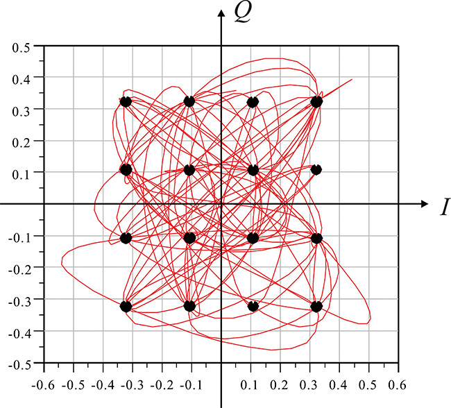
Figure 9E.21 Constellation plot. The trajectory is plotted by Traj and the constellation plot is drawn by Const in Measurement Expression 9E.3. The dots that represent the value at the sample time are at the exact constellation points of 16 QAM.
Next, we need to plot the spectrum of the load voltage Vout shown in Figure 9E.19. In order to obtain the envelope spectrum, the envelope at the fundamental carrier frequency should be converted in a Fourier series. Thus, the equation shown in Measurement Expression 9E.4 is entered in the display window. Vfund is the envelope at the fundamental carrier frequency and the function fs(∙) converts Vfund into a Fourier series.
![]() Spectrum=dBm(fs(Vfund,,,,,“Kaiser”))
Spectrum=dBm(fs(Vfund,,,,,“Kaiser”))
Measurement Expression 9E.4 Equation for obtaining the spectrum of the output voltage
The spectrum is shown in Figure 9E.22. Since the symbol rate in Figure 9E.19 has been set to 24.3 kHz, the spectrum is almost 0 at frequencies beyond the symbol rate. Most of the spectral powers can be observed to be gathered within ± 24.3 kHz. An ACPR calculation is often required for the envelope spectrum, for which the equations shown in Measurement Expression 9E.5 are entered in the display window.
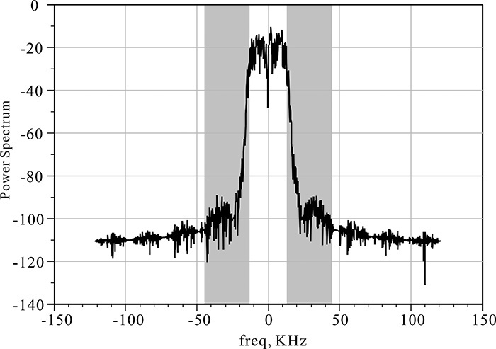
Figure 9E.22 Spectrum of the fundamental frequency envelope. Most of the spectral powers appear within the bandwidth determined by the symbol rate. The shaded frequency bands are the adjacent upper and lower channels. The leakage power to adjacent channels appears, although it is small, and it is specified using the ACPR metric, which calculates for the selected high- and low-side bandwidths.
![]() mainlimits={-16.4 kHz, 16.4 kHz}
mainlimits={-16.4 kHz, 16.4 kHz}
![]() UpChlimits={mainlimits+30 kHz}
UpChlimits={mainlimits+30 kHz}
![]() LoChlimits={mainlimits-30 kHz}
LoChlimits={mainlimits-30 kHz}
![]() Main_Channel_Power = channel_power_vr(Vfund, 50, mainlimits, “Kaiser”)
Main_Channel_Power = channel_power_vr(Vfund, 50, mainlimits, “Kaiser”)
![]() TransACPR=acpr_vr(V_fund, 50, mainlimits, Lochlimits, UpChlimits, “Kaiser”}
TransACPR=acpr_vr(V_fund, 50, mainlimits, Lochlimits, UpChlimits, “Kaiser”}
Measurement Expression 9E.5 Equations entered in the display window to calculate ACPR
The variable mainlimits in Measurement Expression 9E.5 represents the bandwidth. The variable UpChlimits represents the bandwidth moved up by 30 kHz, while the variable LoChlimits represents the bandwidth moved down by 30 kHz. The upper and lower channels are also shown in Figure 9E.22. The function that computes the power within the given bandwidth is channel_power_vr(∙) and is based on the voltage and resistance. Thus, Main_Channel_Power represents the power within the mainlimits bandwidth.
The ACPR, the ratio of the power in the main bandwidth to the powers in the adjacent bandwidths, can be determined by the repeated use of the channel_power_vr(∙)function described above. However, as there is a simple function acpr_vr(∙) in ADS, the ACPR can be determined by using the acpr_vr(∙) function shown in Measurement Expression 9E.5. The Trans_ACPR shown in that expression compares the power in the mainlimits to the powers in the LoChlimits and UpChlimits, and stores the results as Trans_ACPR(1) and Trans_ACPR(2), respectively, in dB. The values of Trans_ACPR(1) and Trans_ACPR(2) are –28.821 dB and –27.016 dB.
Finally, the power of the modulated signal varies with time and this leads to a probability distribution, which can be plotted using the pdf(∙) function of ADS. Here, the output power and the probability distribution are set as shown in the following equations. The resulting probability distribution is shown in Figure 9E.23.
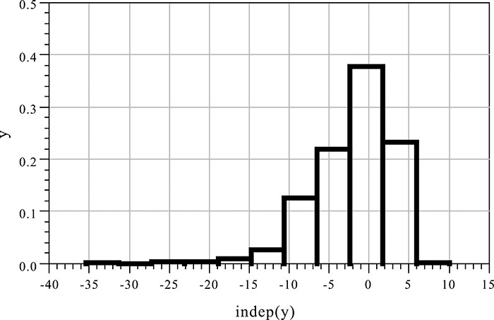
Figure 9E.23 Probability distribution of the modulated signal’s power. Since the average power level is set to 0 dBm using the variable V_peak, the power 0 dBm shows the highest probability.
![]() PdBm=10*log10(mag(Vfund)**2/(2*50))+30
PdBm=10*log10(mag(Vfund)**2/(2*50))+30
![]() y=pdf(PdBm)
y=pdf(PdBm)
Measurement Expression 9E.6 Equations for computation of the probability density function
In Figure 9E.23, the average output power is set to 0 dBm, which can be seen to show the highest probability.
9.6.3 Two-Tone and ACPR Measurements
In the past, the two-tone test was the most commonly used method for evaluating the linearity of power amplifiers. In this method, two CW inputs with the specified frequency spacing are applied to the power amplifier and the output spectrum of the amplifier is then measured. Figure 9.72 shows the measurement method conceptually. When a two-tone signal with a specified frequency spacing is applied to a power amplifier, two distorted signals with the same frequency spacing above and below the two input frequencies appear at the power amplifier’s output. In a communication system using frequency division multiplexing, the frequency spacing corresponds to the channel spacing. The distorted signals appear at the adjacent channels as a result of the power amplifier distortion and they become interference signals to users communicating on the adjacent channels. The distorted signals generally show a third-order relationship to the input power. Therefore, a distorted signal usually increases in proportion to the cube of the input power and has a slope of 3 in a log-log plot. The amplified signal, on the other hand, increases in proportion to the input power. Due to the difference in slope, the extensions of these two lines intersect at a point that is referred to as a TOI (third-order intercept). As an alternative description, the ratio of the amplified signal to the distorted signal is used and is referred to as an IMD3 (third-order intermodulation distortion). The definitions of TOI and IMD3 are shown in Figure 9.73.
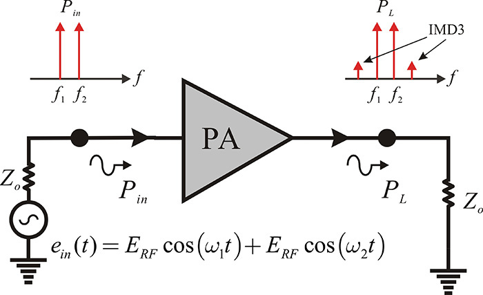
Figure 9.72 Two-tone measurement. Due to third-order nonlinearity, the IMD3 appears at the power amplifier output.
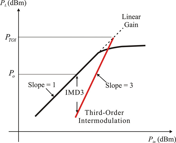
From Figure 9.73, the TOI and IMD3 are not independent and measuring the IMD3 determines the TOI as expressed in Equation (9.63).
Here, Po as a tone output power represents the power at which the IMD3 is measured.
For the power amplifier circuit designed in section 9.5, set the center frequency to 2.5 GHz, the input power per tone to 18 dBm, and the frequency spacing to 10 MHz. Calculate the IMD3 and the TOI. The reason for setting the power per tone to 18 dBm is to set the input power to 21 dBm because the sum of the two input powers of 18 dBm is 21 dBm. Note that the previously designed power amplifier has an output power of 36 dBm when the input power is 21 dBm. Plot the output tone power and the third-order distorted power for the input power change per tone from –10 dBm to 18 dBm.
Solution
After configuring the designed power amplifier circuit as a subcircuit, the ADS P_nTone signal source is used as the input source and the circuit is set up as shown in Figure 9E.24 to observe the two-tone response. In order to view the output tone power and third-order distorted power, after opening the Sweep tab of the Harmonic Balance simulation controller shown in Figure 9E.24, pwr_in is specified as the sweep parameter and adjusted from –10 dBm to 18 dBm in steps of 0.5 dB.
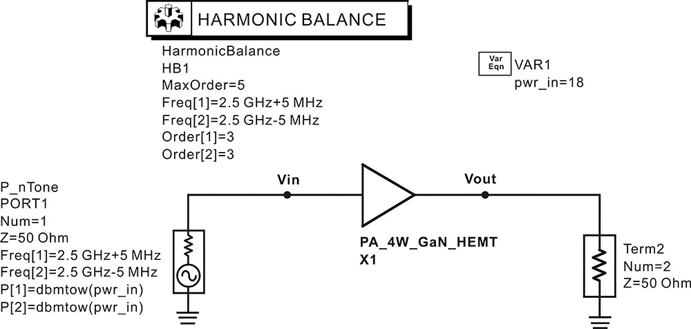
Figure 9E.24 Simulation schematic for the IMD3. Frequency spacing for two-tone simulation is set to 10 MHz. The tone power level is set to 18 dBm because the PA yields 36 dBm at a 21-dBm input power.
The calculated power spectrum at 18-dBm input power is shown in Figure 9E.25. Vout[56,::] corresponds to the output voltage for the input tone power of 18 dBm. The IMD3 in Figure 9E.25 can be seen to be approximately 16 dB. The combined output power of the two-tone signals is computed to be 35.343 (=32.343 + 3) dBm, which is about 1 dB less than the expected power. This is because the output power corresponding to the 1-dB difference is distributed into many spurious components.
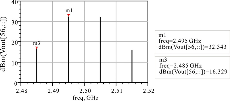
Figure 9E.25 Simulated output spectrum at input power 18 dBm. The 18-dBm input power that corresponds to the sweep index 56 IMD3 is about 16.329 dBm.
In addition, in order to calculate the TOI in accordance with Equation (9.63), the equation in Measurement Expression 9E.7 is entered in the display window, which gives a TOI = 40.35 dBm.
![]() TOI=(3*m1-m3)/2
TOI=(3*m1-m3)/2
The output tone power and the IMD3 power are shown in Figure 9E.26.
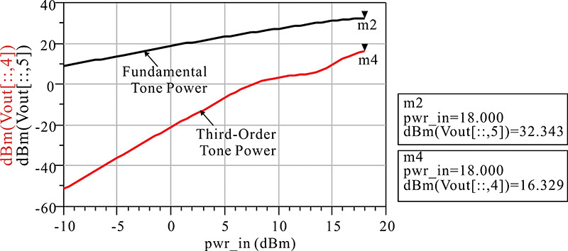
Here, freq[::, 4] corresponds to the frequency of the third-order distortion of 2.485 GHz and freq[::, 5] corresponds to the input frequency of 2.495 GHz. For an 18-dBm tone input power, the tone output power is 32.3 dBm and corresponds to the combined power of the two-tone output power, which is 35.3 dBm. As mentioned earlier, this is lower than the expected output power because a portion of the output power is distributed into many spurious components.
The previously explained two-tone method is the appropriate evaluation tool for the metric of power amplifier linearity used in communication systems employing frequency-division multiplexing. However, the two-tone method does not give direct criteria for power amplifier linearity in digital communication systems. The spectrum of digitally modulated signals is typically spread over a wide frequency range and the two-tone method does not provide a direct evaluation for the interference effects on other channels. As a result, in digital communication systems employing CDMA (code division multiple access), power amplifier linearity is evaluated by ACPR (adjacent channel leakage power ratio). ACPR can generally be defined as
However, although conceptually the same, the ACPR definition may depend on the type of communication system. In addition, various communication systems’ standards are usually referred to in the evaluation of the ACPR of a power amplifier.
The CDMA forward-link signal source in ADS is applied to the input of the power amplifier designed in section 9.5, as shown in Figure 9E.27. Set the input power level of the CDMA forward-link signal source to 12 dBm, which corresponds to a 9-dB back-off from the input power of 21 dBm that yields a 36-dBm output power. Determine the ACPR.
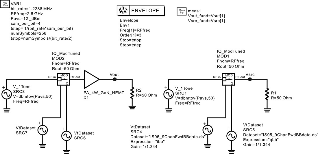
Figure 9E.27 Simulation schematic for calculating the ACPR. The right-hand side obtains the spectrum of the CDMA forward-link source.
Forward link refers to the link from the base station to the handset, while reverse link refers to the link from the handset to the base station. There is a difference between the two links because they use different modulation schemes. The left side of the schematic in Figure 9E.28 shows a CDMA forward-link signal source applied to the designed power amplifier circuit. The circuit at the right side of Figure 9E.27 is inserted for the analysis of the signal source.
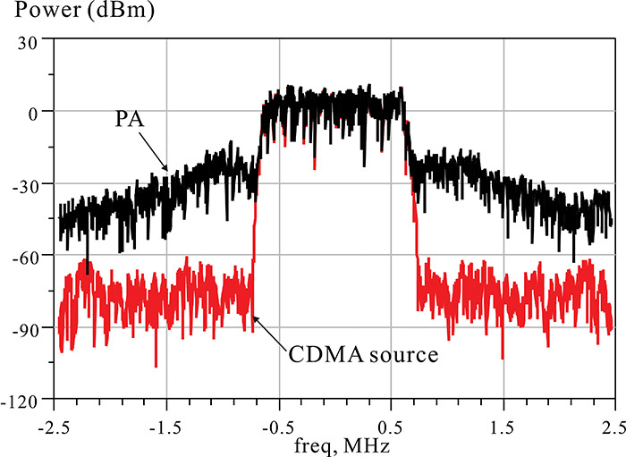
Figure 9E.28 Simulated output spectra. The upper trace is the PA output spectrum, while the lower trace shows the spectrum of the CDMA forward link source. The PA spectrum outside the bandwidth grows significantly.
In Korea, the center frequency of communication systems that employ a CDMA is 1.9 GHz but the center frequency of the designed amplifier is 2.5 GHz. Thus, the center frequency in this example is changed to 2.5 GHz. In addition, to improve the linearity in the designed power amplifier, the input power is set to a 12-dBm back-off of 9 dB from 21 dBm.
The signal shown in Figure 9E.27 represents the signal source modulated by a 1.288-MHz bit rate. The time step of the envelope simulation is defined to be one-quarter of the bit rate. This is the recommended parameter value in ADS. In addition, the number of symbols is set to 256 in order to be able to see all the variations of the signal source. Since the order is 3 in the Harmonic Balance controller, Vout in Figure 9E.27 shows three harmonics. To obtain the fundamental components of Vout and the signal source, Vout_fund=Vout[1], Vsrc_fund=Vsrc[1] are entered in the Measurement Expression shown in Figure 9E.27. Vout_fund and Vsrc_fund thus represent the time-varying envelopes of the fundamental carrier. The signal source and power amplifier output powers within the bandwidth can be calculated by summing the spectral powers within the bandwidth. The ADS function for this purpose is channel_power_vr(·). As explained earlier, this function calculates the power based on the voltage and resistance by summing the spectral powers within the bandwidth. The bandwidth mainCh in Measurement Expression 9E.8 is determined by the given bit_rate. The signal source and power amplifier output powers within the bandwidth can thus be calculated in dBm by entering the following equations in the display window:
![]() mainCh={-(1.2288MHz/2),(1.2288MHz/2)}
mainCh={-(1.2288MHz/2),(1.2288MHz/2)}
![]() PA_pwr=10*log10(channel_power_vr(Vout_fund,50, mainCh, “Kaiser”)+30
PA_pwr=10*log10(channel_power_vr(Vout_fund,50, mainCh, “Kaiser”)+30
![]() Src_pwr=10*log10(channel_power_vr(Vsrc_fund,50, mainCh, “Kaiser”)+30
Src_pwr=10*log10(channel_power_vr(Vsrc_fund,50, mainCh, “Kaiser”)+30
The calculated powers of the power amplifier output and signal source are 31.061 and 14.141 dBm, respectively. In the case of the signal source, the actual signal source power is approximately 2.141 dB larger than the input power set to 12 dBm. Therefore, the gain of the signal source must be reduced. Reducing the gain of the signal source by 1/1.72 results in a signal source power of 11.998 dBm, which is close to the desired input power level. Under this condition, the power amplifier shows an output power of 29.338 dBm. After making these settings and performing the simulation, the equations in Measurement Expression 9E.9 are entered in the display window to determine the signal source and the power amplifier’s output spectrums.
![]() Sp_src=dBm(fs(Vsrc_fund,,,,,“Kaiser”))
Sp_src=dBm(fs(Vsrc_fund,,,,,“Kaiser”))
![]() Sp_PA=dBm(fs(Vout _fund,,,,,“Kaiser”))
Sp_PA=dBm(fs(Vout _fund,,,,,“Kaiser”))
Here, the function fs(·)converts a time-domain function into the frequency-domain spectrum using a Fourier series. Thus, these equations represent the spectra of Vout_fund and Vsrc_fund. Figure 9E.28 shows the spectra obtained from the simulation.
From Figure 9E.28, the adjacent channel leakage power of the signal source is found to be low, while that of the power amplifier output shows a significant increase. This degrades the ACPR performance. As a result, the following equations in Measurement Expression 9E.10 are entered in the display window to calculate the ACPR defined for CDMA communication systems:
![]() UpCh={885 kHz, 915 kHz}
UpCh={885 kHz, 915 kHz}
![]() LoCh={-915 kHz, -885 kHz}
LoCh={-915 kHz, -885 kHz}
![]() ACPR=acpr_vr(Vout_fund, 50, mainCh, LoCh, UpCh,“Kaiser”)
ACPR=acpr_vr(Vout_fund, 50, mainCh, LoCh, UpCh,“Kaiser”)
Function acpr_vr(·) determines the ratio of the powers within the bandwidth and in the upper and lower sidebands. The resulting ACPRs of the power amplifier are –45.96 dBc and –44.03 dBc for the upper and lower sidebands, respectively. It is worth noting that the bandwidths of the upper and lower sidebands are set narrower than the signal bandwidth. The ratio of the signal bandwidth to the bandwidths of the upper and lower sidebands is
If the bandwidth ratio is normalized to 1, the ACPR will be degraded by 16.12 dB.
9.6.4 EVM Simulation
To some extent, the previously described ACPR can be used to assess whether a power amplifier is adequate for a digital communication system; however, the ACPR is still an indirect measure. The most direct method is to measure the BER (bit error rate) when the power amplifier is used in a digital communication system. However, the BER may be affected by the variety of components that constitute the digital communication system, making it difficult to estimate the degradation of the BER coming from the power amplifier alone. Another problem is that BER requires the analysis of more than 106 symbols to find the BER’s degree of degradation. Thus, the computation time for BER simulation increases to an intolerable level. In order to simulate BER efficiently, a DSP (digital signal processing) simulator, which is not discussed in this book, is used together with the envelope simulation. Co-simulation with DSP is an efficient method for BER analysis. Refer to the ADS documentation in reference 6 at the end of this chapter for details. An alternative method is to perform the EVM analysis discussed in section 9.6.1. After the demodulation of the received signal is completed, plotting I(t) and Q(t) at sampling times gives the constellation plot, which jitters around the normal constellation points of I(t) and Q(t) due to distortions in the power amplifier. The power amplifier’s suitability can be determined by looking at the degree of jitter in the constellation points. Of course, in this method as well, the contributions of other components in the communication system can appear, but only the power amplifier’s contribution can be found. In the measurement given by Equation (9.58), the EVM shows the relative jitters of a constellation reference point; thus, the degree of jitter in the constellation points due to the power amplifier can be found using EVM and thereby the suitability of the power amplifier can be determined.
Using the simulation results of the power amplifier circuit in the previous Example, obtain the EVM.
Solution
The same simulation schematic in Figure 9E.27 can be used. For the simulation results obtained from Example 9.12, the equations in Measurement Expression 9E.11 are entered in the display window to obtain the EVM.
![]() time_pts=indep(Vsrc_fund)
time_pts=indep(Vsrc_fund)
![]() tstep=time_pts[1]-time_pts[0]
tstep=time_pts[1]-time_pts[0]
![]() delay = sample_delay_qpsk(Vout_fund, bit_rate[0], 0, tstep)
delay = sample_delay_qpsk(Vout_fund, bit_rate[0], 0, tstep)
![]() data = const_evm(Vsrc_fund, V_fund, bit_rate[0], delay, 0, 0, 0)
data = const_evm(Vsrc_fund, V_fund, bit_rate[0], delay, 0, 0, 0)
The variable time_pts is defined using the independent variable of Vsrc_fund. Thus, time_pts becomes a time variable. Variable tstep is the time step in the envelope simulation. Entering the equations above can be avoided by specifying the output variable as tstep in the output tab of the envelope simulation controller. The optimum sample time may be between 0 and 1/bit_rate = 1/1.2288 MHz = 0.8138 μsec; however it is difficult to find the optimum sampling time manually, which minimizes the jitters of the constellation points. Thus, using the function sample_delay_ qpsk(·), the optimum sampling time can be obtained. The optimum sampling time obtained is 0.2035 μsec. It is also noteworthy that the optimum sampling time depends on the modulation schemes. Since the CDMA forward-link modulation is a QPSK, the optimum sampling time can be calculated using the sample_delay_qpsk(·) function. The function const_evm(•) calculates the EVM by comparing the reference constellation points with the measured constellation points. The EVM results are stored in data in Measurement Expression 9E.11. The output data[0] and data[1] represent the constellation plot and trajectory of the reference signal at the given sample time, while data[2] and data[3] represent the constellation plot and trajectory of the signal to be compared. The constellation plots of the reference signal and those of the signal for comparison are shown in Figure 9E.29, respectively. Next, data[4] shows the error with respect to time, and data[6] shows the value of the EVM as a percentage. The resulting value of data[6] is 3.84%. Small jitters are found to occur at the constellation points compared with the reference QPSK constellation points.
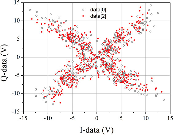
Figure 9E.29 Simulated reference (data[0]) and power amplifier output (data[2]) constellation plots. The function const_evm(·) gives the reference constellation plots as the output variable of index 0 and the constellation plots of comparison signal as the output variable of index 2.
The constellation points appearing at the origin of the IQ plane in Figure 9E.29 are due to QPSK modulation. In that modulation, transitions from (1,1) to (0,0) or from (0,1) to (1,0) cause the trajectory to pass through the origin in the IQ plane, which results in the constellation points near the origin in the plane. Such transitions make the value of the envelope 0 and cause a large amplitude change. Therefore, PAPR (peak-to-average power ratio) becomes larger, which causes problems in the efficient driving of the power amplifier. This can be solved using the π/4-DQPSK modulation scheme. Refer to references 2 and 5 at the end of this chapter for more details.
9.7 Composite Power Amplifiers
As mentioned previously, most power amplifiers distort the input signal to some degree. Thus, the linearity of a given power amplifier may be the key issue in determining its applicability in a communication system. Most power amplifiers have a satisfactory linearity at a low-output power level; however, significant distortion occurs as the output power approaches saturation. To avoid this problem in the past, it was common practice to use the power amplifier at an output power level backed off (by a certain amount) from the saturated power. Usually, a 3-dB back-off power level from the saturated power was widely used. However, with the use of digitally modulated signals today, a higher back-off output power level is required. The higher back-off output power level is very unsatisfactory, considering the cost-effectiveness of the active device. RF methods such as predistorter and feed-forward techniques are commonly used to improve the linearity. Another method is based on recent advances in digital signal processing techniques that can decompose the input signal to the power amplifier into envelope- and phase-modulated carriers. The power amplifier is then set to amplify only the phase-modulated carrier while the envelope controls the amplifier’s power supply, thereby improving the amplifier’s linearity and efficiency. This technique is called an EER (envelope elimination and restoration). This method will be summarized in this section.
In addition, the efficiency of the power amplifier generally improves as the output power level approaches saturation; however, communication systems employing digitally modulated signals are mostly operated at low power. In addition, the power amplifier is rarely operated at its maximum output power. In this case, as the power amplifier is used mainly at the output power level with low efficiency, the amplifier’s efficiency significantly drops. Thus, a power amplifier with high efficiency at a wide input power range is required and one such amplifier is the Doherty. The operation of the Doherty amplifier will be briefly discussed in this section.
9.7.1 Predistorters
Figure 9.74 shows a power amplifier with a predistorter.
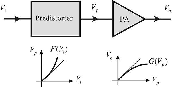
Figure 9.74 Concept of predistorter. The predistorter that compensates for the power amplifier’s saturation helps to improve the amplifier’s linearity.
In Figure 9.74, Vi, Vp, and Vo represent the voltage amplitudes of the fundamental frequency. The typical Vo–Vp characteristic of a power amplifier is also shown in Figure 9.74. The output voltage departs from the straight line as the input voltage increases and enters saturation. If the output voltage Vp of the predistorter increases as Vi increases, as shown in Figure 9.74, the entire input-output characteristic of the system will show linearity. As a result, the linear characteristic can be improved. Figure 9.75 shows the method of obtaining the required input-output characteristic of the predistorter for a linear power amplifier. In Figure 9.75(a), the power amplifier has an output power PL,1 for an input power Pin,1 (point A). In order to align this to the straight line, the output power PL,2 corresponding to point B must appear at the output. The output power PL,2 appears at the output for an input power Pin,2 instead of Pin,1, corresponding to point C. Therefore, for an input power of Pin,1, the predistorter should produce Pin,2. By repeating this process, the predistorter required for the linear power amplifier can be obtained and the linear output power range of the power amplifier can be increased up to the saturation point.
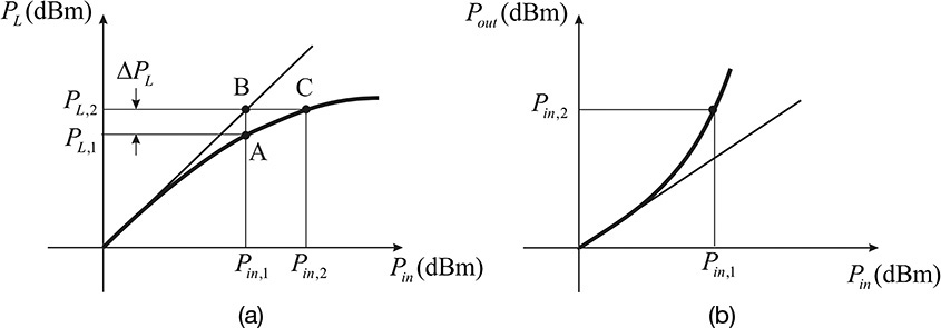
Figure 9.75 (a) Input and output characteristic of a power amplifier and (b) input and output characteristic of a predistorter. Using the PL–Pin plot of the PA, the desired Pout–Pin characteristic of the predistorter can be computed.
In the previous explanation, three questions must be considered:
1. Is it possible to implement such a predistorter with the specified input-output characteristic?
2. The method in Figure 9.75 is possible only when the input-output characteristic of the power amplifier is assumed to be purely resistive. Can this method still be applied when the input-output characteristic of the power amplifier is not purely resistive?
3. When configured in this way, is the linearity improvement truly achieved?
For the first question, various configurations for the predistorter are possible. For example, it can be implemented using a diode. Assuming the diode to be a purely nonlinear resistive device, it can be considered as an open circuit for a low-input power level, and as an approximate short circuit for a higher input power. Thus, using this property of the diode, the predistorter can be constructed using a well-known branch-line coupler, as shown in Figure 9.76.
Figure 9.76 A predistorter using a branch-line coupler. For a small input power, the two diodes can be approximated as open and the small input power appears at the output due to mismatch by RA. However, for a large input power, the two diodes approximately operate as short and the output power is almost equal to the input power due to reflection by the two diodes.
If RA is close to the port impedance of the branch-line coupler, the predistorter provides a linear-attenuated output power due to a small mismatch by resistor RA. Here, the diode is approximated as an open circuit because the RF input power level is low. Thus, the input-output characteristic is considered to be approximately linear. On the other hand, as the diode comes close to being a short circuit for a high RF input power, total reflection occurs from the diode and the sum of the two reflected powers appears at the output. This combined power will be close to the input power level. Thus, the attenuation is high when the input is low and the input-output characteristic is linear. On the other hand, when the input power level is high, the input-output characteristic shows a gain closer to 1. Thus, an appropriate input-output characteristic for the predistorter can be obtained. By adjusting the values of the devices in Figure 9.76, a predistorter having the required characteristic of Figure 9.75(b) can be designed. There are a variety of predistorter circuits and more details about them can be found in reference 2 at the end of this chapter.
For the second question, the distortion of power amplifiers requires further analysis. In the explanation above, by viewing the distortion of the power amplifier as purely resistive, the output voltage of the power amplifier vL in terms of the input voltage can be written by Equation (9.64).
When the input is a sinusoidal voltage given by vin = V1cosωt, by substituting this into Equation (9.64), the fundamental component of VL = Fund(vL(t)) can be rewritten as Equation (9.65).

Here, depending on the sign of the coefficient a3, the input-output characteristic shown in Figure 9.75(a) can be obtained. However, in general, the power amplifier does not take the form of Equation (9.64). It is commonly known that a time delay appears at the third-order term. Therefore, Equation (9.64) can be rewritten as Equation (9.66).
Thus, substituting the sinusoidal input vin = V1cosωt, and rearranging the fundamental component, it can be written as Equation (9.67).
In this case, the previous resistive-predistorter design method may not work due to the differences in the phases of the fundamental and third-order distortion terms. However, the predistorter used in combination with a phase-shifter can improve the linearity of the power amplifier. This Solution is somewhat complicated, but is theoretically possible by expanding the input-output relation of the power amplifier in the form of Equation (9.66). Reference 2 at the end of this chapter can be consulted for more information.
The third question can be proved using the two-tone method. By substituting a two-tone signal into Equation (9.66) and expanding the equation, the third-order term can be removed and the linearity is clearly improved; as a result, the linearity for other modulation signals will also be improved. An ACPR improvement by 10–20 dB has reportedly been achieved, as shown in Figure 9.77. This method is simple but widely used for power amplifier linearization, and the literature currently describes several other methods.
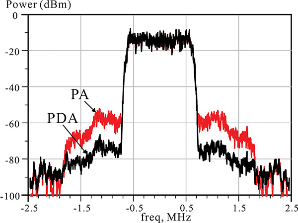
Figure 9.77 ACPR improvement of a power amplifier with a predistorter for digital modulation signal. The digital modulation signal is a IS95 forward-link signal. The spectra of the PDA (predistorted power amplifier) and power amplifier alone are compared. The adjacent power level is reduced by about 20 dB.
Given that the input-output characteristic of a power amplifier is expressed as vL = a1vi – a3(vi)3, where a1 = 10 and a3 = 0.109a1, design an appropriate predistorter. In addition, compare the input-output characteristics of the power amplifiers with and without the designed predistorter. In addition, compare the output powers of the two power amplifiers for a two-tone input of a tone power Pin = 10 dB.
Solution
Suppose that the input-output characteristic of the predistorter is vp = vi + b3(vi)3 and substituting this into vi,
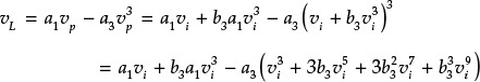
The third-order term must be removed, which results in b3 = a3/a1. This is configured through the VCVS (voltage-controlled voltage source) in ADS, as shown in Figure 9E.30. The simulated Pout–Pin characteristic is shown in Figure 9E.31. From Figure 9E.31, the power amplifier with the predistorter is found to show an improved 1-dB compression point compared with the original power amplifier.
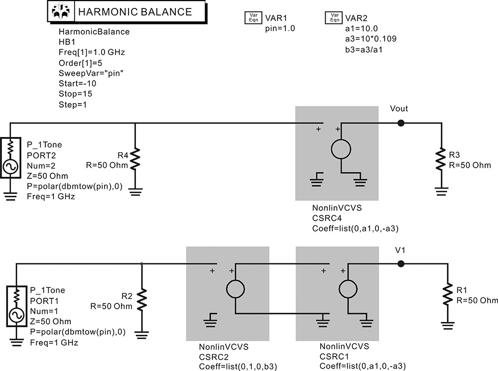
Figure 9E.30 Comparison of the input-output characteristics of the power amplifiers with and without predistorters. The top circuit models PA while the bottom circuit models PDA.
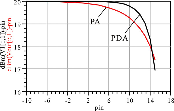
Figure 9E.31 Comparison of the simulated gain characteristics. From the plot, we can find the 1-dB compression point is increased in the case of the PDA.
Next, the simulation is carried out for the two-tone input signal with a center frequency of 2.5 GHz, a frequency spacing of 10 MHz, and a tone power of 10 dBm. The two simulated spectra for the power amplifier and the power amplifier with the predistorter are shown in Figure 9E.32. The IMD3 of the power amplifier with the predistorter in Figure 9E.32 is found to be improved by about 20 dB.
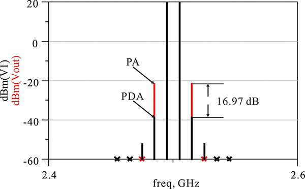
The linearity of the power amplifier is clearly improved in this example. However, it should be noted that the ACPR is somewhat poorer due to the contribution of the higher-order terms of the predistorter when the input power is not sufficiently backed off, especially in the case of digitally modulated signals such as CDMA.
9.7.2 Feedforward Power Amplifiers (FPA)
The basic concept of a feedforward power amplifier is to remove the distortion signal IMD3 that appears at the output of the power amplifier by adding an inverted distortion signal. When a two-tone signal is applied to the power amplifier’s input, distorted signal components appear at the power amplifier’s output due to the third-order distortion, as shown in Figure 9.78. By adding a signal whose magnitude is equal and the phase is 180° out of phase to the distortion signal, the distortion signal will disappear from the output and only the amplified components of the input signal will appear at the output.
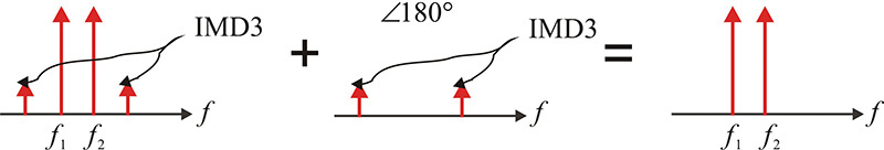
Figure 9.78 Concept of a feedforward power amplifier. The 180° out-of-phase IMD3 signal is generated and added to the PA output. Consequently, the IMD3 signal at the PA output disappears and linearity is improved.
The feedforward power amplifier is the implementation of this concept and is shown in Figure 9.79.
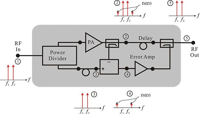
In Figure 9.79, when a two-tone signal is applied to ![]() , the amplified two-tone signal with the IMD3 appears at the output of the power amplifier,
, the amplified two-tone signal with the IMD3 appears at the output of the power amplifier, ![]() . In contrast, a distortion-free two-tone signal with an appropriate delay appears at
. In contrast, a distortion-free two-tone signal with an appropriate delay appears at ![]() . Assuming the delay line offers a phase delay such that the two two-tone signals at
. Assuming the delay line offers a phase delay such that the two two-tone signals at ![]() and
and ![]() have a phase difference of 180°, the resulting sum of the two signals appearing at
have a phase difference of 180°, the resulting sum of the two signals appearing at ![]() will be a pure IMD3 signal, as shown in the figure. Since the magnitude of the IMD3 signal is generally small, after being sufficiently amplified by the error amplifier, the two signals are combined at the power amplifier’s output. Thus, an amplified two-tone signal alone appears at the output of the power amplifier at
will be a pure IMD3 signal, as shown in the figure. Since the magnitude of the IMD3 signal is generally small, after being sufficiently amplified by the error amplifier, the two signals are combined at the power amplifier’s output. Thus, an amplified two-tone signal alone appears at the output of the power amplifier at ![]() , as shown in the figure. In order to make the phase difference of 180° between the two IMD3 signals, a delay line is inserted at the output of the power amplifier.
, as shown in the figure. In order to make the phase difference of 180° between the two IMD3 signals, a delay line is inserted at the output of the power amplifier.
Thus, the feedforward power amplifier can be experimentally designed using a two-tone input. There may be a disadvantage to this method in that the linearity performance is easily degraded by environmental changes because the adjusted condition to eliminate the distorted signal depends on the conditions of many components. In addition, since the condition is satisfied for selected two-tone input frequencies, the IMD3 elimination condition can also be broken when the frequency changes. Therefore, the bandwidth of the feedforward power amplifier can, in principle, only be a narrow one. In general, this type of amplifier is reported to show more improvement in linearity in a narrow bandwidth than does a predistorted power amplifier.
9.7.3 EER (Envelope Elimination and Restoration)
In 1950, the EER method was proposed by Kahn; in it, instead of directly amplifying the amplitude-modulated signals, the power amplifier amplifies a CW signal, and the power amplifier’s DC supply varies according to the amplitude-modulation signal, thereby improving the amplifier’s efficiency. Generally, the power amplifier shows better efficiency when a constant-amplitude square-wave input is applied. In addition, the higher the input power, the better the improvement in the efficiency. Therefore, by using EER, a dramatic improvement in the efficiency of the power amplifier can be achieved.
However, unlike conventional amplitude modulation, both the amplitude and phase of a carrier changes in modern digitally modulated signals. It is not easy to separate the amplitude-modulation and phase-modulation components. However, using digital signal processing, as shown in Figure 9.80, the modulation signal can be separated into the signals that require amplitude and phase modulations. The phase modulation is independently performed for the sinusoidal input and is applied to the power amplifier’s input. Thus, the power amplifier amplifies only the phase-modulated signal. On the other hand, the DC supply of the power amplifier varies according to the envelope signal and, using this type of amplification, the efficiency of the power amplifier can be improved.
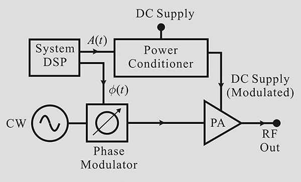
Figure 9.80 EER block diagram. The modulation signal is first decomposed into the amplitude and phase. The decomposed phase then modulates the CW signal and the phase-modulated signal is amplified by the PA. Thus, the PA operates in the high-efficiency region. The amplitude modulation is carried out using a DC power supply modulation.
In the case of a fast modulation signal, the EER structure is not easy to implement because the DC supply of the power amplifier generally changes slowly. The power amplifier usually requires a large current, from a few amperes to several tens of amperes, and a DC supply voltage from as much as a few volts to typically several tens of kV. Therefore, varying this amount of power supply voltage according to the modulation signal is not an easy task. In addition, because the DC voltage for a power amplifier is generally supplied through a bypass capacitor, that capacitor significantly limits the high-frequency modulation signal.
9.7.4 Doherty Power Amplifier
Figure 9.81 shows the probability distribution of the output power of a power amplifier in a handset employing CDMA (code division multiple access). The power amplifier is driven for linear amplification from –25 dBm to 25 dBm, and the maximum output power is set to be 25 dBm. Note that, for the most part, the output power level in the power range of –5 dBm–5 dBm is used and the frequency using the maximum output power of 25 dBm is very low. Generally, the maximum efficiency is shown near the maximum output power of 25 dBm, at which the efficiency is about 30–50% and the efficiency rapidly falls with a decrease in the output power, which makes the power consumption increase considerably.
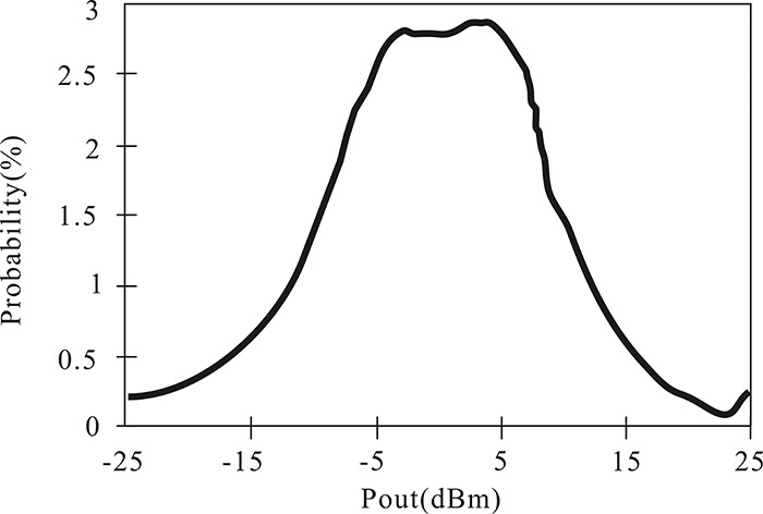
Figure 9.81 Probability distribution of CDMA (drawn after the reference).11 The maximum power level of the PA is about 25 dBm but most of the PA’s usage is at about a 0-dBm power level. As a result, the PA operates at low efficiency.
11. G. Hanington, P-F Chen, et al., “High-Efficiency Power Amplifier Using Dynamic Power-Supply Voltage for CDMA Applications,” IEEE Transactions on Microwave Theory and Techniques 47, no. 8 (August 1999): 1471–1476.
Figure 9.82 shows the efficiencies of a class-B power amplifier and Doherty amplifier with respect to input power. The x–axis is scaled in decibels. In the case of the class-B power amplifier, the efficiency rapidly increases with respect to the input power. Therefore, when a class-B power amplifier is employed in a system having the output-power probability distribution shown in Figure 9.81, the power amplifier will operate at low efficiency for most of the time. In contrast, the Doherty amplifier maintains efficiency at maximum output power within a significant input power range even when the input power is low. Thus, when the operation requires better efficiency for a wide range of input power, the Doherty amplifier appears to be the ideal choice. A multistage Doherty amplifier can be used to further improve the range of this efficiency. Refer to reference 2 at the end of this chapter for more information.
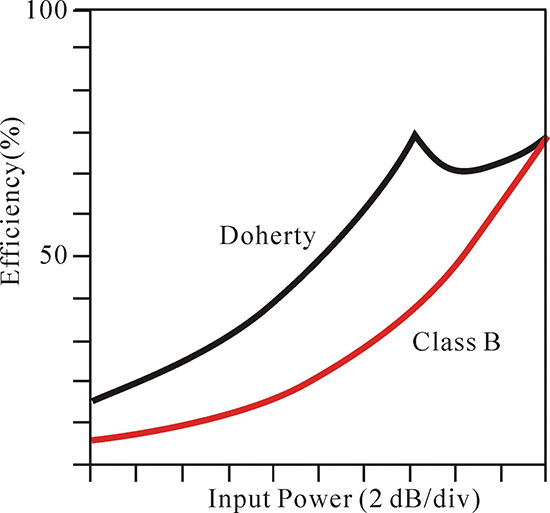
Figure 9.82 Comparison of the efficiencies for Doherty and class-B power amplifiers with respect to input power. The Doherty PA maintains high efficiency down to the 6-dB input power level.
Figure 9.83 shows the structure of the Doherty power amplifier. Two active devices are used in the power amplifier; the device used as “Main” is biased as class-B using the DC supply voltage Vbm; the device marked as “Peaking” is usually biased as class-C by adjusting the DC voltage Vbp. In addition, all the transmission lines used in the input and output are one-quarter-wavelength long. The two active devices used in the Doherty amplifiers may be different due to their costs or specifications; however, for this discussion it is assumed that both devices are the same.
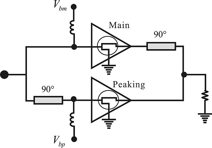
Figure 9.83 Doherty power amplifier. “Main” is a class-B power amplifier while “Peaking” is a class-C power amplifier.
Figure 9.84 shows the normalized drain currents versus input voltage for the devices “Main” and “Peaking,” which operate in class-B and -C, respectively. The drain current waveform of the class-B power amplifier has a sinusoidal-tip shape. The drain current Im in Figure 9.84 represents the fundamental component of the sinusoidal-tip-shaped waveform. A plot of Ip versus the input voltage can be similarly interpreted. The drain current Im linearly increases from 0 with respect to the input voltage because the device “Main” is biased as class-B. However, in the case of Ip for the device “Peaking,” the drain current Ip does not flow below a certain level of the input voltage because it is biased as class-C. The current Ip begins to increase with respect to the input voltage beyond the threshold voltage. In Figure 9.84, the “Peaking” device is so biased in class-C such that no output current flows below Vin = 0.5. In addition, denoting the maximum values of Im and Ip as IM and IP, respectively, the normalized drain currents Im and Ip by IM and IP are shown in Figure 9.84. It is also assumed that IM = IP. Thus, denoting the normalized input voltage Vin as x(0 < x < 1), Im and Ip can be expressed as shown in Equations (9.68) and (9.69).

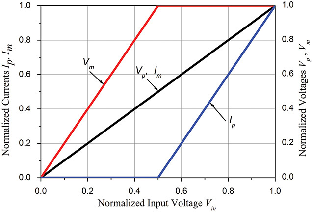
Figure 9.84 The “Main” and “Peaking” output voltages and currents versus the input voltage in the Doherty amplifier. This plot shows the typical characteristics of a 6-dB Doherty PA.
In order to analyze the combined output of the “Main” and “Peaking” devices in Figure 9.84, the equivalent circuit of the Doherty amplifier’s output from Figure 9.83 is drawn in Figure 9.85. The current sources Im and –jIp in Figure 9.85 represent the currents arising from the drains of the “Main” and “Peaking” devices, respectively. The drain current of the “Peaking” device is phase-delayed by 90° due to the phase delay of the input voltage, as shown in Figure 9.85.
Figure 9.85 Model of the Doherty amplifier output. Im represents the class-B half-wave current source of the “Main” device while Ip represents the class-C sinusoidal tip waveform of the “Peaking” device. The phase factor –j appears as a result of the quarter-wavelength transmission line.
The transmission line is represented by ABCD parameters as expressed in Equation (9.70).
From Equation (9.70), it can be seen that Vp = –jZoIm. Thus, as shown in Figure 9.84, the drain voltage Vp of the “Peaking” device has the same dependence on the input voltage as Im. The drain voltage Vp reaches the maximum value for Im = IM, and the maximum voltage of Vp is denoted as VM. Then, the magnitude of Vp normalized by VM can be plotted against the input voltage, which is the straight line of Im shown in Figure 9.84. Using Equation (9.70) again, V1 can be expressed as Equation (9.71).

Because Ip = 0 for x < 0.5, there is no contribution of Ip up to x = 0.5 in Equation (9.71). Setting (Zo)2/R to reach the maximum output voltage VM at x = 0.5, the drain voltage Vm of the “Main” device will reach maximum voltage VM at x = 0.5, as shown Figure 9.84. Since the “Peaking” device is in the off state, the efficiency of the “Main” device becomes the efficiency of the Doherty amplifier below x < 0.5. For x > 0.5, the “Peaking” device turns on and the drain current Ip flows. The voltage Vm changes due to the contribution of the current Ip and generally becomes a piecewise line. As the signs of the two terms in Equation (9.71) are different, they are found to cancel out each other. If the further increase by Im is exactly cancelled by Ip for x > 0.5, the drain voltage Vm of the “Main” device maintains the maximum output voltage VM at the normalized input voltage of 0.5. Thus, the plot of Vm appears, as shown in Figure 9.84. The cancellation of the two terms in Equation (9.71) is done to make the two terms have the same slopes for x. Since the slope of Ip is 2 for x, (Zo)2/R should be equal to 2Zo in order to cancel out each other. Thus, the relationship in Equation (9.72) is satisfied.
Because Zo = 2R in Equation (9.72), the efficiency of the “Main” device when operating as a class-B amplifier decreases for x > 0.5; however, the efficiency of the “Peaking” device when operating as a class-C amplifier increases as x increases. As a result, the Doherty amplifier maintains an approximately constant efficiency in the range of 0.5 < x < 1. The efficiency of the Doherty amplifier can be calculated from the Fourier series of class-B and class-C amplifiers explained in section 9.4.1. Since Figure 9.84 represents the amplitude of the fundamental component, the DC current component can be calculated using Equations (9.8) and (9.9a). The DC components of the “Main” and “Peaking” devices Im,0 and Ip,0 are expressed in Equations (9.73) and (9.74).
Here, the conduction angle is θ = cos-1(0.5). Thus, setting the DC drain supply voltage to VDD = 1, the normalized DC power consumption can be obtained with Equation (9.75).
The RF output power is determined by computing the power supplied by the two current sources of Figure 9.85. The RF output power is given by
From Equation (9.76), the efficiency is calculated as shown in Equation (9.77).
The DC power consumption computed using the DC current calculated from Equations (9.73) and (9.74) and the RF power calculated from Equation (9.76) are shown in Table 9.13.
Figure 9.86 is a plot of the calculated efficiencies in Table 9.13. Considering that the Doherty amplifier is normally used in the high-efficiency range starting from the normalized input voltage Vin = 0.5, it means that the Doherty amplifier in Figure 9.86 provides high efficiency up to 6-dB back-off input power. The peak of the efficiency at Vin = 0.5 can be moved by adjusting the conduction angle; using this method, a Doherty power amplifier with various ranges of back-off input power can be achieved.
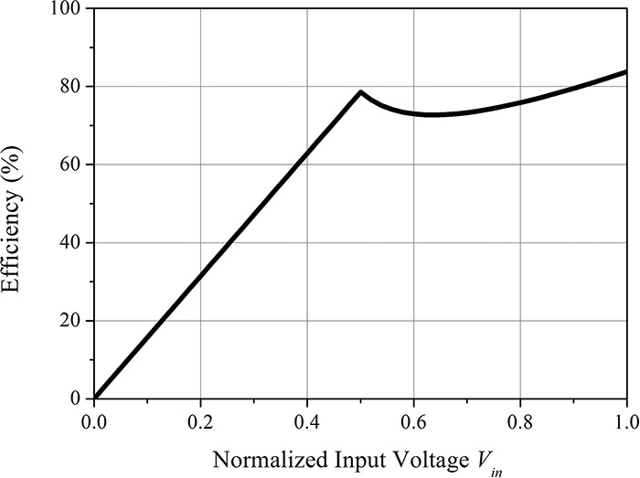
Figure 9.86 The calculated efficiency of the Doherty amplifier. High efficiency is maintained down to Vin = 0.5.
Using the half-wave current source, calculate the efficiency and output power of the Doherty power amplifier in Figure 9.85 with ADS.
Solution
The equivalent circuit of the output in Figure 9.85 consists of two half-wave current sources, which can be implemented using Equations (9.8) and (9.9). Figure 9E.33 shows the “Main” and “Peaking” half-wave current sources implemented by using those equations. Since the output of the “Peaking” amplifier has a 90° phase delay at the fundamental frequency fo, the phase delay is implemented using the pd(x) function that provides the phase delay of n × 90° at the n-th harmonic frequency. In addition, the two current sources are made to provide the same peak current values of 1 A and the conduction angle of the “Peaking” current source is set to θ = cos–1(0.5).

Figure 9E.34 shows the simulated waveforms of the current sources. The “Main” current source has the half-wave shape and its maximum value of 1 A is shown in Figure 9E.34. On the other hand, the “Peaking” current source has a phase delay of 90° compared with the “Main” current source, and its maximum value is also 1 A as expected. The conduction angle can be found from the width of the sinusoidal-tip-shaped waveform, and it is estimated to be about half of the “Main.” Thus, the conduction angle can be found to be θ = cos–1(0.5).

Figure 9E.34 Class-B and class-C simulated output current waveforms. The voltage VC is delayed by a phase of 90°.
Using the current sources thus obtained, the equivalent circuit of the Doherty amplifier’s output can be configured as shown in Figure 9E.35.
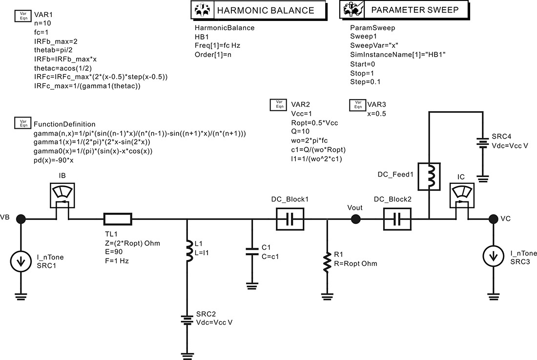
Figure 9E.35 Simulation schematic of the Doherty amplifier’s output. L1 and C1 are parallel resonant at the fundamental frequency. SRC1 is the half-wave current source, while SRC3 is the current source of the sinusoidal-tip-shaped waveform.
First, in Figure 9E.35, IRFb_max is set to 2. IRFb_max corresponds to the maximum peak value of the “Main” current source that has the half-wave shape. The value of Im in Figure 9.84 is the value of the fundamental amplitude when the half-wave-shape current is expanded into a Fourier series. The value of Im is one-half of the half-wave peak value. Thus, since IRFb_max = 2, the maximum value of Im is set to 1 A. Similarly, Ip in Figure 9.84 is the fundamental amplitude of the “Peaking” current source when the “Peaking” current is expanded into a Fourier series. The ratio of Ip to the peak value of the “Peaking” current source is γ1(θ). To make the maximum value of Ip to 1 A, the peak value IRFc_max of the “Peaking” current source is set to IRFc_max = 1/gamma1(thetac).
The variable x represents Vin in Figure 9.84, which corresponds to the fundamental amplitude of the input voltage. The change of Im for Vin is set to IRFb_max*x, by which the “Main” current varies in proportion to Vin. The “Peaking” current source can be also made to vary according to Vin. To implement Ip for Vin in Figure 9.84, Ip is set to IRFc_max*(2*(x–0.5)*step(x–0.5)) because its slope is 2 and its non-zero value appears at the value of above x = 0.5.
L1 and C1 in Figure 9E.35 constitute a parallel resonant circuit and its Q is set to 10. Using Equation (9.72), the transmission line impedance is set to Z = 2 * Ropt. The value of Ropt can be determined from the Doherty amplifier characteristics in Figure 9.84. When Im is 0.5 A, the drain voltage of “Main”, Vm, should be 1 V. Using Vm = Im(Zo)2/Ropt in Equation (9.71), 0.5 × (Zo)2/Ropt = 4Ropt × 0.5 = 1. Thus, it can be found that Ropt = 0.5 Ω. After the settings, it must be verified whether or not the circuit of Figure 9E.36 has the Doherty amplifier characteristics shown in Figure 9.84. The values of Im, Ip, Vm, and Vp are computed and plotted for Vin as shown in Figure 9E.36. The plot is found to show the Doherty amplifier characteristics in Figure 9.84.
Figure 9E.36 Simulated output current and voltage characteristics of the Doherty amplifier. Here, B stands for class-B and C stands for class-C. VC[::,1], VB[::,1], IC.i[::,1], and IB.i[::,1] are the fundamental voltages and currents for the sweep variable x.
The following equations in Measurement Expression 9E.12 are entered in the display window to compute the efficiency, which is plotted as shown in Figure 9E.37. It can be seen that the efficiency in Figure 9E.37 is the same as that computed in Figure 9.86.
![]() Pdc=mag(SRC2.i[::,0]+SRC4.i[::,0])
Pdc=mag(SRC2.i[::,0]+SRC4.i[::,0])
![]() Pout=0.5*mag(Vout[::,1])**2/Ropt[0]
Pout=0.5*mag(Vout[::,1])**2/Ropt[0]
![]() eff=Pout/Pdc*100
eff=Pout/Pdc*100
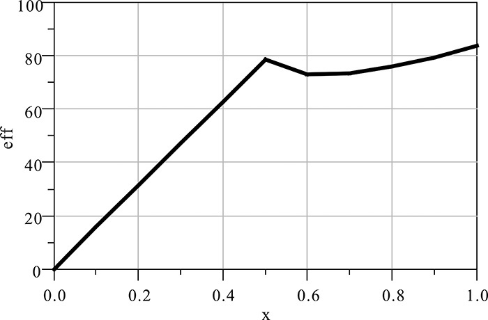
Figure 9E.37 Simulated efficiency for the sweep variable x of the Doherty amplifier. The simulated efficiency is found to be equal to that in Figure 9.86.
In addition, in order to know the maximum current capability of the active devices, the output waveforms of the “Main” and “Peaking” current sources are plotted with Vin as a parameter. The variations of the currents are shown in Figure 9E.38. In the case of the “Main” amplifier in Figure 9E.38(a), a maximum current capability of 2 A is required, while in the case of the “Peaking” amplifier operating in class-C, a maximum current capability of 2.5 A is required. The waveform of the output voltage Vout with Vin as a parameter is shown in Figure 9E.38(b); the output voltage is close to a sinusoidal waveform due to the effect of the parallel resonant circuit, as expected.
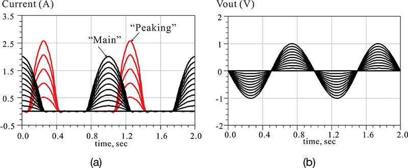
Figure 9E.38 (a) Class-B and class-C current waveforms and (b) output voltage Vout with respect to input
9.8 Summary
• The power amplifier (PA) is a key component that determines the transmitting power level of a transmitter. The design of the PA is fundamentally different from that of an LNA. The load impedance is selected to meet the output power, efficiency, harmonics, and distortion.
• The active devices such as GaN HEMT and LDMOSFET that are widely used for PAs are introduced. GaN has a wide bandgap and good thermal conductivity, which leads to a high breakdown voltage and a high power dissipation capability. As a result, a GaN HEMT is an appropriate device for a high-power amplifier.
• The Si LDMOSFET is a device with a breakdown voltage that is improved through drain engineering. However, due to the low electron mobility of Si, its use is primarily limited to applications with frequencies below 4 GHz.
• The optimum load impedance of an active device is experimentally obtained from a load-pull measurement setup that employs impedance tuners. Alternatively, the optimum load impedance can be obtained through a load-pull simulation when the large-signal model of an active device is available. In the load-pull simulation, harmonic impedances should be taken into consideration.
• Power amplifiers can be classified into class-A, -B, -C, -D, -E, and -F. A class-A PA provides high linearity; however, its efficiency is limited to 50% or less. A class-B PA eliminates the stand-by power consumption of the class-A PA and its efficiency is below 78.5%. Moving the operating point further from the pinch-off results in the class-C PA provides a higher efficiency than does the class-B PA; however, from the output power point of view, the power capability of the active device is not fully exploited.
• Class-D and -E PAs operate with a transistor as a switch and their efficiency can reach 100%. However, they lose the amplitude information. A class-E PA employs the detuned resonator circuit. Using the class-E PA, the drain or collector voltage does not show an abrupt transition or possible device damage, and an efficiency drop can be avoided.
• A class-F PA uses multiple resonators in the load to flatten the drain voltage. The maximally flat and maximum efficiency waveforms for limited harmonics are derived. They can be used to estimate the efficiency and optimum resistance of a class-F PA.
• A design example of a class-F PA using the TriQuint GaN HEMT model is demonstrated. The design follows these steps:
1. Stabilize the device
2. Obtain the optimum source and load impedance extraction using load-pull simulation
3. Implement the input matching circuit and a class-F load matching circuit using lumped-element matching circuits
4. Replace the lumped-element matching circuits with the physical layout components
5. Tune the implemented matching circuits through EM simulation
6. Verify the EM-simulated matching circuits
• Power amplifier evaluation methods and specifications for linearity are presented. The two-tone, ACPR, and EVM methods are described.
• A power amplifier’s linearity can be improved by building a composite PA. Predistorter, feedforward, and EER techniques are used to improve PA linearity.
• The high-efficiency range of a power amplifier can be extended by using a Doherty power amplifier. Using a simplified example, we demonstrate that the amplifier’s high-efficiency range can be extended.
• The power amplifier is a key component of a communication system and it is constantly attracting the interest of many researchers. Because power amplifier design is a field in which new concepts are continuously emerging, the readers should keep abreast of recent research results.
References
1. A. Howard, Load Pull Simulation Using ADS. Available at ADS directory: ADS_Home/examples/RF_Board/LodaPull_prj/LoadPullPres.pdf, 2002.
2. S. C. Cripps, Advanced Techniques in RF Power Amplifier Design, Boston: Artech House, Inc., 2002.
3. A. Grebennikov and N. O. Sokal, Switchmode RF Power Amplifiers, Amsterdam: Elsevier, 2007.
4. TriQuint semiconductor. TriQuint EEHEMT model implemented in ADS and AWR for TQT 0.25 um 3MI GaN on SiC process 1.25 mm discrete FET. April, 2009.
5. S.C. Cripps, RF Power Amplifiers for Wireless Communications, Boston: Artech House, Inc., 1999.
6. Agilent Technologies, Advanced design system 2009U1. Available at http://www.keysight.com/en/pd-1612226/ads-2009-update-1?cc=US&lc=eng, 2009.
Problems
9.1 Instead of the following variable declaration for the impedance tuner, use the step(•) function and implement the LoadTuner.
![]() global Impedance Equations
global Impedance Equations
;Tuner reflection coefficient
LoadTuner=LoadArray[iload]
LoadArray=list(0,rho,fg(Z_l_2),fg(Z_l_3),fg(Z_l_4),fg(Z_l_5))
iload=int(min(abs(freq)/RFfreq+1.5,length(LoadArray)))
fg(x)=(x-Z0)/(x+Z0)
9.2 Prove that the optimum load resistance value of a class-C power amplifier is
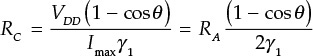
Then, normalizing the output power by the maximum output power of a class-A amplifier, prove that the following ratio is obtained.
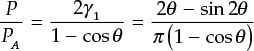
9.3 (ADS problem) Using the output circuit of the class-B power amplifier shown in Example 9.5, and fixing the load resistance value as the resistance value that gives maximum output power, plot the output power versus the input power. In the plot, consider the input power as the output power of the fundamental frequency. Compare this result with the results of Figure 9.25 and discuss the reasons for the difference.
9.4 (ADS problem) Consider the BJT of the voltage-switching class-D amplifier shown in Figure 9P.1 as an ideal switch; using ADS, show that the output voltage VL appears as a sinusoidal voltage. Set the Q of the series resonant circuit to be more than 10.
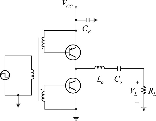
Figure 9P.1 Class-D push-pull amplifier for problem 9.4
9.5 (ADS problem) In the single-ended class-D amplifier circuit shown in Figure 9.26, simulate the circuit using ADS with the DC block capacitor replaced by a high Q-series resonant circuit. Explain why the result is different from that of problem 9.4.
9.6 Prove Equation (9.32).
9.7 The harmonic impedance Zn of the class-E amplifier can be expressed by inspection as shown below. Explain why. Another way to express this is for Zn to expand vn(t) and in(t) into a Fourier series and Zn can then be determined from the ratio of the Fourier series of vn(t) and in(t) at the same frequency.
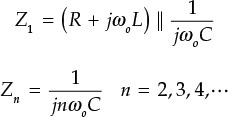
9.8 Figure 9P.2 is a class-E amplifier. For operating in the optimum condition, the following relationship must be satisfied (see reference 3, above).
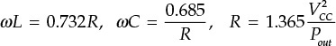
Then, setting fo = 1, Pout = 1, and VCC = 1, plot the waveforms of v(t), i(t), and vout(t).
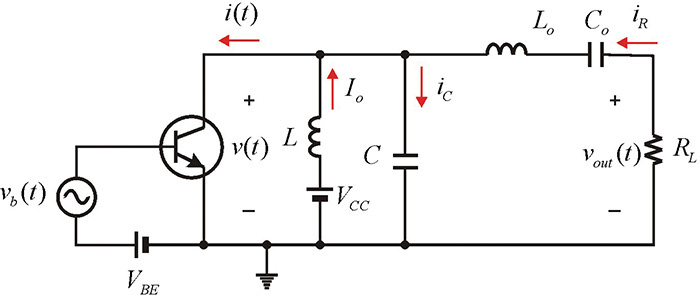
9.9 Prove that the value of b that satisfies Equation (9.39) is b = 0.1667.
9.10 Calculate the power capability, Mp, of the class-E amplifier in Figure 9.35. Compare this with the power capability of the ideal class-F amplifier.
9.11 For the following amplifier in Figure 9P.3, given that power supply voltage VCC = 10 V, and the maximum current Imax = 1 A, determine the optimum impedance, Ropt, for maximum efficiency using Tables 9.4, 9.5, and 9.6.
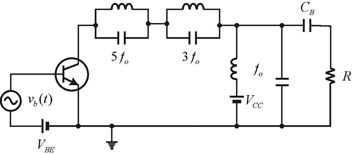
9.12 In the following circuit in Figure 9P.4, given that the Lo–Co has a high-Q and resonates at the frequency ωo and that it has the following settings for the output matching circuit,12
12. A.V. Grebennikov, “Effective Circuit Design Techniques to Increase MOSFET Power Amplifier Efficiency,” Microwave Journal 43, no. 7 (July 2000): 64–72.
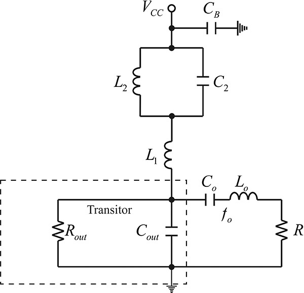
Calculate the maximum efficiency.
9.13 (ADS problem) The circuit of Figure 9P.5 is an example of an ideal class-F amplifier. By considering the output of the active device as a switch, plot the waveforms of v(t), i(t), and vout(t). Now given that the L1 – C1 resonates at the fundamental frequency fo, set a high value for Q and then simulate.
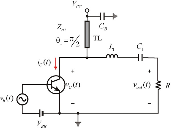
9.14 Discuss the π/4-DQPSK modulation scheme, and explain why PAPR (Peak to Average Power Ratio) in this scheme can be improved.
9.15 A pre-distorter with the input-output characteristics given by vp=vin+b3(vin)3 is to be used to linearize the power amplifier represented by the input-output characteristics given by vL = a1 vp – a3(vp)3. In order to linearize the amplifier, prove that b3=a3/a1. With such a pre-distorter, the output voltage characteristic of the power amplifier is represented by the 5th, 7th, and 9th distorted terms; determine the coefficient of the 5th term.
9.16 For a power amplifier and a predistorter modeled by vL = a1 vp(t)–a3(vp(t–τ))3, and vp = vin(t)–b3(vin(t–τ’))3 respectively, find a relation for a sinusoidal input to eliminate the third-order term at the amplifier output.
9.17 In the pre-distorter with vp = vin(t)–b3(vin(t–τ’))3, the third order term design requires the conditioning of amplitude and phase. When only the third-order term can be separately extracted, the design of the pre-distorter is made easy, which is called a “cuber” in reference 2. Propose the block diagram to extract the third-order term of the predistorter.
9.18 The most general approach for modeling the power amplifier will be the recently developed X-parameter method. Search X-parameters on the Web.
9.19 (ADS problem) In this chapter, the 6-dB back-off Doherty amplifier was explained, which maintains a high efficiency even at 6-dB back-off power. By a similar concept, a 10 dB back-off Doherty amplifier is also possible. Calculate the efficiency characteristics of this amplifier.