
Chapter 11. Phase-Locked Loops
11.1 Introduction
The direct application of most microwave oscillators, previously described in Chapter 10, to a communication system is seldom possible because their phase noises are generally not low enough. The phase noise is associated with frequency jitters in the time domain. As the phase noise of the microwave oscillator is typically high, the frequency jitter also increases significantly with time. The large-frequency jitter prevents the direct use of the microwave oscillator in a communication system. In addition, the microwave oscillator’s phase or frequency in a communication system is often modulated and then that modulated signal is transmitted or received. Thus, the microwave oscillator’s phase noise also limits the phase or frequency modulations necessary for communication.
A crystal oscillator is known to be the most stable oscillator to date and most communication systems require a phase noise as low as that provided by the crystal oscillator. However, it is not possible to fabricate crystal oscillators beyond a few hundred MHz. In contrast, microwave oscillators can be fabricated for high-frequency applications albeit with poor phase noise. The comparison of the phase noises of a 10-GHz VCO (voltage-controlled oscillator) and 10-MHz crystal oscillator (its frequency is multiplied by a factor of 1000 to obtain 10 GHz) is shown in Figure 11.1.

Figure 11.1 Phase noise of a PLL. The phase noise output for an optimally set loop bandwidth follows the minimum between the phase noise of a 10-GHz VCO and that of the crystal oscillator whose frequency is multiplied by a factor of 1000 to attain a frequency 10 GHz.
In that figure, the optimum frequency source may be one that has the phase noise of the crystal oscillator for a low offset frequency, while it follows the phase noise of the VCO for a high offset frequency. The optimum phase noise characteristic is shown by a solid line in the figure. The frequency source with the optimum phase noise characteristic in Figure 11.1 can be implemented using a PLL (phase-locked loop). In addition, a frequency source whose frequency increases or decreases with a specified frequency step (usually referred to as a channel) is usually required in communication systems. This type of frequency source is referred to a frequency synthesizer that can be configured using a PLL. In this chapter, the configuration and basic operation of a PLL will be discussed.
11.2 Configuration and Operation of a PLL
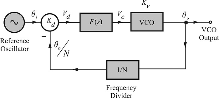
The configuration of a PLL is shown in Figure 11.2. The reference oscillator is usually a crystal oscillator that oscillates at a fixed frequency and provides the reference frequency. The phase of the reference oscillator is represented by θi, while that of the VCO is represented by θv. The phase noise of the VCO is represented by θn, which is shown as a separate noise source added to the phase of the VCO. Therefore, the output phase of the VCO is expressed in Equation (11.1).

Figure 11.2 PLL configuration; the phase noise of the VCO is represented by an additive noise source θn. The PLL output is θo.
Since the oscillation frequency of the VCO, ωv, varies according to the tuning voltage Vc, it can be expressed using θv with Equation (11.2).
Expressing Equation (11.2) in a Laplace transform gives Equation (11.3).
Here, Kv is termed the tuning sensitivity of the VCO, and its unit is [rad/sec·V]. The phase detector in Figure 11.2 is a device that converts the phase difference between the two input signals into a voltage and its proportionality constant is termed a phase detector constant Kd. Thus, denoting the output voltage of the phase detector as Vd, we obtain Equation (11.4).
The dimension of Kd is thus [V/rad]. Note that the output voltage of the phase detector is a slow time-varying voltage close to the DC voltage. The low-pass filter connected to the phase detector is called the loop filter and its function is to remove the harmonics that appear in the phase detector. F(s) represents the transfer function of the loop filter.
In order to examine the operation of the PLL in Figure 11.2, first consider the case of F(s) = 1, and θn = 0, which results in Vc = Vd. Assuming that the steady state is reached, the tuning voltage Vc of the VCO is no longer considered to vary with time. If Vc varies with time, then the assumption of the steady state would be violated. Therefore, the output voltage of the phase detector Vd does not vary with time. Thus, the phase error θε at the steady state is expressed in Equation (11.5).
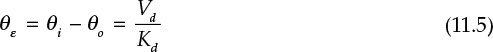
Under the steady state condition, since Vd is a DC voltage that no longer varies with time, then differentiating both sides of Equation (11.5) gives Equation (11.6).
Thus, when F(s) = 1, the frequency of the VCO is found to be equal to that of the reference oscillator; however, it should be noted that the reference oscillator and the VCO have a phase difference given by Equation (11.5). Initially, the frequencies of the VCO and reference oscillator are different prior to reaching the steady state and a tuning voltage proportional to the phase difference is then formed that drives the frequency of the VCO to a value equal to that of the reference oscillator. As a result, the tuning voltage of the VCO should be established to make the frequency of the VCO equal to the frequency of the reference oscillator and the phase error defined by Equation (11.5) inevitably occurs when F(s) = 1.
This phase error can be removed by implementing F(s) with an integrator. However, even with the integrator, the frequency of the VCO should not be time-varying at the steady state and subsequently the tuning voltage, Vc, of the VCO does not become time-varying. Since the tuning voltage Vc in Figure 11.2 is the output of the integrator, that output is therefore constant and independent of time at the steady state. Thus, the input of the integrator must be zero. If that input is not zero, then by integrating the non-zero input with respect to time, the output will consequently vary with time.
When the input is positive, the output of the integrator increases with time while it decreases with time when the input is negative. As a result, the integrator output will vary with time. Since the integrator output is the tuning voltage Vc, that tuning voltage varies with time, which violates the assumption of a steady state. Therefore, by simply inserting an integrator into the PLL circuit, the phase error given by Equation (11.5) becomes 0, that is, θε = 0. As a result, when an integrator is used as a loop filter, not only the phases but also the frequencies of the two oscillators are made equal. The VCO is thus synchronized with the frequency and phase of the reference crystal oscillator.
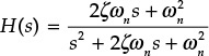
Next, we examine the phase noise of the PLL’s output (and also the VCO’s output). Here, setting K = Kd Kv, the PLL output θo is computed as shown in Equation (11.7).

Here, H(s) represents the closed-loop gain of the PLL. Since the output phase noise consists of two independent noises θi and θn, the PLL output phase noise can be written as Equation (11.8).
In general, since the closed-loop transfer function H(s) → 1 when s → 0 and H(s) → 0 when s → ∞, H(s) thus shows the characteristic of a low-pass filter. The phase noise of the PLL output from Equation (11.8) follows the phase noise of the reference oscillator within the bandwidth of H(s), while it follows the phase noise of the VCO outside the bandwidth of H(s). That is, the expression above can be approximately written as Equation (11.9).

Thus, the phase noise of the PLL’s output can be determined using Equation (11.8). This is plotted as shown in Figure 11.3.

Figure 11.3 Phase noise of the PLL’s output. Within the loop bandwidth, the phase noise of the PLL follows that of the reference oscillator, while it follows the VCO’s phase noise outside the bandwidth.
A PLL is configured using a 10-MHz crystal oscillator and a 10-GHz VCO, each having the phase noise shown in Table 11E.1.

The frequency of the 10-MHz crystal oscillator is multiplied by 1000 and it is used as the reference oscillator. The closed-loop transfer function is expressed as
Plot the phase noise of the PLL output for ζ = 0.707, fn = 1 kHz, and 10 kHz (ωn = 2πfn).
The phase noise of the PLL output is computed using ![]() and is shown in Figure 11E.1.
and is shown in Figure 11E.1.

Figure 11E.1 PLL output phase noise. When the loop bandwidth is smaller than the intercept point of the two phase noises, then the PLL phase noise floor in the loop bandwidth is raised.
The bandwidth BW of H(s) is defined by (BW) = ωn/(2π). From Figure 11E.1, the phase noise of the PLL output follows the phase noise of the crystal oscillator below the bandwidth, as expected, and it follows the phase noise of the VCO above the bandwidth. Note that the phase noise floor rises for a small bandwidth such as 1 kHz. Therefore, a bandwidth of approximately 40 kHz, which is the intersection of the two phase noise curves, is appropriate for obtaining the optimum phase noise. As in the example, the PLL bandwidth (BW) can be selected for the optimum phase noise; however, the BW is sometimes determined by considering both spurious attenuation and lock time.
The phase noise of a 10-MHz OCXO (oven-controlled crystal oscillator) and that of a 100-MHz VCXO (voltage-controlled crystal oscillator) are shown in Table 11E.2. It is necessary to phase-lock the VCXO to the OCXO (its frequency multiplied by 10) using a PLL. Determine the optimum bandwidth and the approximate phase noise characteristic of the phase-locked VCXO.

Solution
In order for the frequencies of the OCXO and VCXO to be equal, it is necessary to multiply the frequency of the OCXO by 10. Denoting the phase noise of the OCXO as LOXCO(f), then the phase noise multiplied by a factor of 10 is
LOCXO(f) + 20 log 10 = LOCXO(f) + 20
The phase noise of a 100-MHz OCXO is shown in the second column of Table 11E.3. In addition, for the purpose of comparison, the phase noise of the 100-MHz VCXO is shown in the third column. Then, using an ideal loop filter that yields |H(s)| = 1 inside the loop bandwidth while |H(s)| = 0 outside the loop bandwidth, the phase noise output of the phase-locked VCXO is found by selecting the minimum of the two phase noises in the second and third columns. A plot of the phase noises of the 100-MHz OCXO and of the VCXO in Table 11E.3 are shown in Figure 11E.2. Both the phase noises can be seen to be equal at an offset frequency of 100 Hz, which is thus the optimum loop bandwidth. In addition, the minimum of the two phase noise curves in the figure becomes the phase noise output of the phase-locked VCXO.


Figure 11E.2 Phase noises of a 100-MHz VCXO and a 100-MHz OCXO with respect to offset frequency. The optimal loop bandwidth for the PLL phase noise is about 100 Hz.
To configure the PLL in Figure 11.2, the frequencies of the VCO and of the reference oscillator must be equal. This is practically impossible to achieve as it is common for the reference oscillator’s frequency to be low, while the VCO’s is usually high. The problem can be solved by using a frequency multiplier or frequency divider in the PLL. The frequency divider is often used to configure the frequency synthesizer. Two configurations of the PLL using the frequency divider are shown in Figure 11.4.
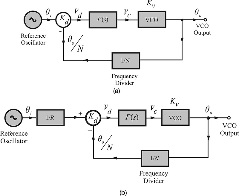
Figure 11.4 Frequency synthesizers; the frequency of the reference oscillator is (a) undivided and (b) divided by R
The operations of the two PLLs can be explained using the steady-state concept. Assuming the loop filters in Figure 11.4(a) and 11.4(b) are implemented using a kind of integrator, the output voltage of the phase detector will be zero in the steady-state. Thus, in the case of the frequency synthesizers shown in Figure 11.4(a), Equation (11.10) is satisfied.
The output frequency of the PLL can be obtained by differentiating Equation (11.10) with respect to time, which results in ωo = Nωi. Thus, the PLL output frequency can be obtained by multiplying the frequency of the reference oscillator by N. In addition, from Equation (11.9), the output phase noise is equal to the phase noise of the reference oscillator (multiplied by N) in the loop bandwidth, while it is equal to the phase noise of the VCO outside the loop bandwidth.
In the case of the reference oscillator shown in Figure 11.4(b), whose frequency is R-divided, Equation (11.11) is written by the same method as
Therefore, by varying the frequency division ratio, a frequency corresponding to integer multiples of the frequency step ωi/R becomes the output frequency. At the same time, the phase noise of the reference oscillator multiplied by N/R is obtained inside the loop bandwidth, while outside the bandwidth, the phase noise of the VCO is obtained.
Calculate the output frequency of the PLL with the configuration shown in Figure 11E.3.

Solution
Assuming a steady state, the output of the phase detector is 0 and the frequencies of the two input signals of the phase detector are equal. Therefore, the output frequency of the mixer becomes
fIF = 8 × 124 MHz
and the output frequency of the VCO is
fv = fIF + 34.3 = 35.292 GHz
11.3 PLL Components
The key components in a PLL include a VCO (voltage-controlled oscillator), a loop filter, a phase detector, and a frequency divider. Since we have already discussed the VCO in Chapter 10, in this section we will focus on the phase detector and frequency divider.
11.3.1 Phase Detector
In the past, due to the limitations in semiconductor manufacturing technology, it was not possible to fabricate high-speed logic circuits. DBMs (doubly balanced mixers) were widely used as high frequency phase detectors. However, thanks to recent technological breakthroughs, high-speed logic circuits can be fabricated for use as high-frequency phase detectors. The detailed configuration and characteristics of a DBM will be discussed in the next chapter. In this section, although the DBM is not widely used as a phase detector, we will briefly discuss the characteristics of a DBM phase detector and compare it with the high-speed phase detectors that use logic circuits. A DBM phase detector is shown in Figure 11.5.

The output voltage vIF(t) of the DBM in Figure 11.5 can be written as Equation (11.12).
It should be noted here that vIF(t) in Equation (11.12) is independent of the LO signal amplitude, VREF. This is possible when the amplitude VREF of the LO signal in Figure 11.5 is sufficiently large. As a result, the output vIF(t) is proportional only to the RF signal amplitude, VRF. Also note that vIF(t) is composed of two components: the frequency up-converted and down-converted components. However, only the down-converted components are used as the output of phase detector. Thus, when the frequencies of the LO and RF signals are equal, the output of the phase detector is expressed in Equation (11.13),
which is proportional to the cosine of the phase difference between the two signals. Therefore, the output of the DBM phase detector acts as shown in Figure 11.6.

Figure 11.6 Output voltage of a DBM phase detector. The positive slope appears around 3π/2 and the negative slope around π/2. Depending on the VCO’s tuning characteristics, the slope of the phase detector can be chosen.
From Figure 11.6, the output of the phase detector has a period of 2π for the phase difference between the two signals, and it has a positive slope in the range of +180°-+360°. Therefore, phase-locking is possible for the phase difference in the range of +180°-+360°, but the linear range appears in a narrow range around 270°. The output voltage of the phase detector is 0 when the phase difference is 270°, and thus the reference signal and the VCO synchronize with the phase difference of 90° when a DBM phase detector is used in a PLL. As is obvious from Equation (11.13), the disadvantage of the DBM phase detector is that the linear range occurs only in a limited range of the phase difference. Also, because the phase detector constant is proportional to the RF amplitude, the RF amplitude should be kept constant to preserve the phase detector constant given by the Kv = KLVRF constant.
A 500-MHz reference oscillator with a power of 10 dBm and a 500.010-MHz signal with a power of 0 dBm are applied to the LO and RF inputs of the DBM phase detector. At the phase detector’s output, a peak-to-peak voltage of 100 mV and a 10-kHz sinusoidal waveform appear when measured with an oscilloscope. What is the value of the phase detector constant Kd?
Solution
A 10-kHz sinusoidal waveform and a 100-mV peak-to-peak voltage can be expressed as Vpcos(ωt + φ1), where Vp = 50 mV. Thus, from Equation (11.13), Vbpeak = Vp, and Vbpeak = 50 mV. When the frequencies of the two signals are made equal, and the phase difference between the two signals is set to 90°+φ, the phase detector output becomes Vd ≅ Vbpeakφ. Thus, Kd = Vbpeak and Kd = 50 mV/rad is obtained.
The DBM phase detector operates as a linear phase detector for a small phase difference. The linear range of the phase detector can be significantly increased by implementing the phase detector that uses logic circuits, and a typical example is the Exclusive OR (XOR) phase detector shown in Figure 11.7.
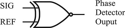
As shown in Table 11.1, the XOR gives the logical output for the two logical signal inputs. Consider the supply voltage VCC and 0 (GND) as the logic values that correspond to H (logic high) and L (logic low), respectively. Therefore, the XOR output yields H (VCC) for the logic inputs pairs (H, L) or (L, H). When two waveforms with the same frequency are applied to the inputs of the XOR, the XOR output waveform appears, as shown in Figure 11.8. When the XOR is viewed as a phase detector, its output is the average DC voltage of the output waveform also shown in Figure 11.8.

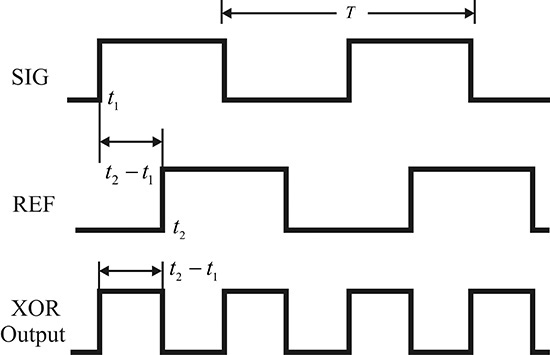
Figure 11.8 Output waveform of an XOR phase detector. The time average or DC component of the XOR output is proportional to the phase difference between SIG and REF.
From Figure 11.8, the output waveform shows two pulse tips per period T. The width and amplitude are t2 - t1 and VCC, respectively. Thus, the average DC voltage can be expressed as Equation (11.14a).

Here, θ corresponds to the phase difference between the two signals, and the phase detector constant is given by
Therefore, the XOR phase detector gives an output that is proportional to θ and has a phase detector constant given by Equation (11.14b).
When the two inputs applied to the XOR phase detector have a phase difference of less than 180°, the output voltage increases in proportion to the phase difference, as shown in Figure 11.9. Conversely, when the phase difference is greater than 180°, the phase detector output decreases as shown in Figure 11.9. From that figure, phase detector voltage Vd,1 arises for two phase difference values θ1, and θ2. An XOR phase detector does not have a one-to-one correspondence with the phase difference. The reason for this phenomenon is that the two pulse tips occur per period as a result of the XOR’s operation. Therefore, the XOR phase detector can be used as a phase detector with a positive slope for a phase difference range of 0° < θ < 180°.

Another type of phase detector can be constructed that uses a sequential logic circuit, as shown in Figure 11.10. The phase detector in that figure is usually referred to as a PFD (phase frequency detector). The PFD can be configured with various sequential logic circuits.
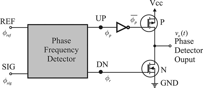
Figure 11.10 PFD (phase frequency detector) circuit. When the UP signal is high, the PMOS (p-type MOS) is on and the output voltage is high. When the DN is high, the NMOS (n-type MOS) is on and the output voltage is low. Otherwise, both MOSs are open and the output voltage is VCC/2 (a high impedance state).
If the reference signal (REF) is leading when compared to the comparison signal (SIG), as shown in Figure 11.11(a), the UP output of the PFD in Figure 11.10 climbs to H at the rising edge of the REF signal and falls to L at the rising edge of the SIG. Conversely, if the comparison signal is leading when compared to the REF signal, as shown in Figure 11.11(b), the DN output climbs to H at the rising edge of the SIG and falls to L at the rising edge of the REF signal. In addition, when the UP is in the H-state, the DN shows no change even at the rising edge of SIG. Similarly, when the DN is in the H-state, the UP shows no change even at the rising edge of REF.
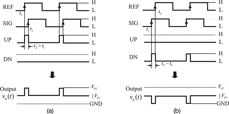
Thus, for the UP and DN outputs, the phase detector output voltage vo(t) will appear as shown in Figs. 11.11(a) and (b), respectively. Note that in the absence of input, vo(t) stays at one-half of the supply voltage. In this state, the external circuit is also cut off from the PFD circuit and is said to be in a high impedance state.
Thus, for input waveforms of the same frequency, the PFD yields a pulse tip only once in a period, as shown in Figure 11.11. Since the phase detector output is the average DC voltage of vo(t), it can be expressed as Equation (11.15)

and the output is proportional to θ. This is shown in Figure 11.12.

Figure 11.12 Phase detector voltage of PFD with respect to phase difference. The PFD has a one-to-one correspondence between the phase detector voltage output and the phase difference.
Note that the phase detector output is at its maximum when the phase difference between the two waveforms is 360º; also note that the phase detector voltage has a one-to-one relationship with the phase difference in the range of 0°-360°. In addition, compared with the other phase detectors previously discussed, the PFD is found to operate as a linear phase detector for a wide range of phase difference.
Note that the PFD output appears as a voltage. When the output of the phase detector is a voltage, an ideal integrator for the loop filter is difficult to implement with passive components. Thus, a current drive circuit is inserted at the end of the PFD shown in Figure 11.13. The circuit in that figure provides a constant current Ip flowing toward the load when the UP is H, whereas the constant current Ip flows from the load when the DN is H. With such a configuration, the phase detector voltage Vd of Equation (11.15) is converted to a current Id and the relationship between the phase detector output current and the phase difference is written as Equation (11.16).

Figure 11.13 PFD circuit with a charge pump. The charge pump circuit makes the constant current flow out of the phase detector output when the UP is high. In contrast, the constant current flows into the phase detector output when the DN is high.
The current drive circuit is called a charge pump. Modern phase detectors are configured by connecting a charge pump to the PFD and the phase detector then provides a current proportional to the phase difference. With this type of configuration, the tuning voltage of the VCO becomes the phase detector current multiplied by the impedance of an external loop filter (Vc = IdZ(s)), which drives the VCO. The integrator can thus be implemented with a simple capacitor. By easily connecting a capacitor to the phase detector in Figure 11.13, the tuning voltage becomes the integral of the phase detector current. However, in the case of the voltage-type phase detector, an integrator cannot be implemented with a simple capacitor.
What is the phase detector constant when the output current Ip in the Do output of Figure 11.13 is 5 mA?
Solution
As described earlier, the PFD provides a voltage output proportional to the phase difference and that voltage output is converted to a current output using a charge pump. However, the output of a typical phase detector is accompanied by a noise floor that can cause problems in the detection of the phase difference. Usually, the larger the frequency division ratio becomes, the smaller the phase noise of the frequency divided by the output of the VCO. The smaller divided phase noise is then applied to the input of a phase detector, which may be less than the noise floor of the phase detector. If the divided phase noise of the VCO is less than that noise floor, the output of the phase detector is simply its own background noise and the desired phase difference cannot be obtained.
The noise floor of a PFD phase detector is usually presented as a specification of the phase detector and an example of the PFD noise floor is shown in Figure 11.14. In that figure, when the comparison frequency increases, the noise floor of the phase detector also increases. The specification of the phase detector is usually defined as the phase detector noise at a comparison frequency of 1 Hz. Therefore, at a comparison frequency of fr, the noise floor of the phase detector can be empirically expressed as

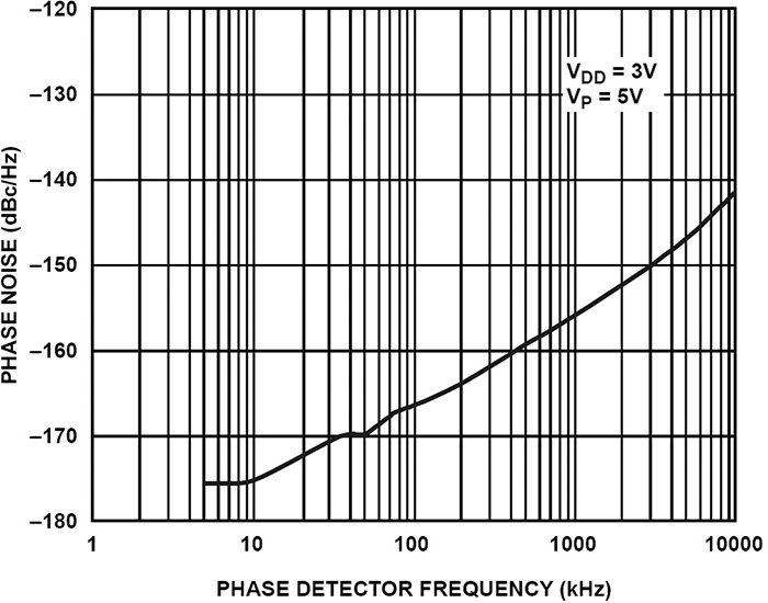
Figure 11.14 Noise floor of the phase detector. (Source: Analog Devices, RF PLL Frequency Synthesizers ADF4110/4111/4112/4113, August 2012.)
The empirical Equation (11.17) can be verified using Figure 11.14, in which the noise floor of the PFD at a comparison frequency of 10 kHz and 100 kHz is about -175 dBc/Hz and -165 dBc/Hz, respectively. Because of this, the PFD noise floor increases by 10 dB due to a decade change of the comparison frequency. Equation (11.17) clearly shows the computed decade change of the noise floor. Therefore, when the noise floor at an arbitrary comparison frequency is known, then the noise floor at all other comparison frequencies can be determined using Equation (11.17).
To examine the effect of the phase detector noise floor, consider the case in which the frequency of the VCO is divided by N in order to lower the VCO frequency to the comparison frequency. Denoting the phase noise of the VCO as φv(f), the divided phase noise of the VCO is φv(f)/N2. Also, denoting the noise floor of the phase detector as φPD, the phase detector provides an output proportional to the phase difference for the frequency-divided VCO input when the phase noise of the VCO is greater than φPD; this is given by
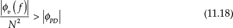
For noise levels lower than the value given by Equation (11.18), the phase detector comparison function is disabled. Equation (11.18) can then determine the offset frequency fm of the VCO. Since the phase noise of the VCO increases as the frequency offset approaches 0 below fm, the phase detector provides an output proportional to the VCO phase noise, while the phase detector provides an output corresponding to its noise floor above fm. In addition, as the division ratio N in Equation (11.18) gets larger, the phase detector provides an output proportional to the VCO phase noise for only a narrow range of the offset frequency.
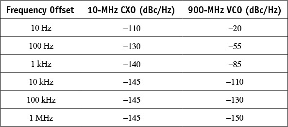
A 900-MHz frequency synthesizer must be configured using a 900-MHz VCO and a 10-MHz crystal oscillator, both of which have the phase noise values shown in Table 11E.4. The normalized noise floor of the phase detector used in the PLL at 1 Hz is -210 dBc/Hz and the comparison frequency is 50 kHz. Calculate the bandwidth of a loop filter that is appropriate for the optimum phase noise output; also calculate the output phase noise of the 900-MHz frequency synthesizer. In addition, compare the output phase noise in this Example when the phase detector has no background noise.
Solution
Denoting the phase noise of the 10-MHz reference oscillator, which is a function of the offset frequency f, as L(f), the phase noise at the comparison frequency of 50 kHz is L(f) + 20log(0.05/10). This is shown in the second column of Table 11E.5. Similarly, the phase noise of the VCO can be calculated by dividing its frequency by the comparison frequency of 50 kHz. The phase noise of a 50-kHz VCO is shown in the fifth column of Table 11E.5.
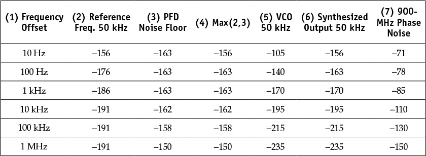
Also, since the noise floor of the given phase detector at 1 Hz is -210 dBc/Hz, the noise floor of the phase detector at the comparison frequency of 50 kHz can be calculated from Equation (11.17), from which a noise floor of -163 dBc/Hz is obtained. The noise floor value corresponds to the case in which the frequency offset is 0. The noise floor values are shown in the third column of Table 11E.5. The noise floor value appears to be constant up to the frequency offset of 1 kHz, which is not far from the comparison frequency, but the noise floor values significantly change above a frequency offset of 10 kHz.
The phase noise of the reference oscillator is independent of the phase detector noise floor. The maximum of the reference oscillator’s phase noise and phase detector’s noise floor becomes the new reference phase noise that is shown in the fourth column. Therefore, the phase noise synthesized by the PLL is obtained by comparing the newly defined reference phase noise and the VCO phase noise at 50 kHz. The minimum of the newly defined reference phase noise and the VCO phase noise becomes the phase noise of the frequency synthesizer. Comparing columns 4 and 5, the intersection is found to occur between 100 Hz-1 kHz. Thus, setting the loop bandwidth to approximately 100 Hz-1 kHz will give the optimum results. The synthesized phase noise at 900 MHz is thus calculated using the synthesized phase noise at 50 kHz by multiplying the latter by n = 900/0.05 = 18,000. This is shown in the last column of Table 11E.6.
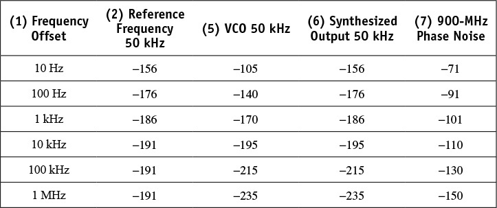
In contrast, in the absence of the background noise in the phase detector, the values of the phase noise can be calculated in the same way as in Example 11.2. This is summarized in Table 11E.6. From that table, due to the effect of the phase detector noise floor on the frequency synthesizer, a difference of about 20 dB can be seen to occur between the frequency offset of 100 Hz-1 kHz.
11.3.2 Frequency Divider
Most frequency dividers are implemented using digital counters. In this section, we will explain a frequency divider that is based on the operation of digital counters; however, the discussion will not include details of the digital counter circuits. The operation of a frequency divider is shown in Figure 11.15. When the VCO input shown in that figure is applied to the frequency divider’s input, the frequency divider shows changes only at the rising edges of the VCO waveform. When the rising edge is detected, toggling from a previous state to another state occurs. That is, the frequency divider changes to the “high” state if it was in the “low” state and vice versa. Through the toggling operation, the VCO frequency divided by 2 appears as an output, as in the second waveform shown in Figure 11.15. In addition, with continuous repetition of the process, waveforms whose frequencies are divided by 4, 8, 16, and so on, can be obtained. In this operation, the toggling is assumed to occur only at the rising edge of the VCO waveform. However, for some digital circuits the toggling can occur at the falling edges of the input and the frequency divider can be implemented with that falling-edge toggling.

Generally, there are two types of frequency dividers: a fixed divider (with a fixed division ratio such as /2, /4, /8, and so on, as shown in Figure 11.15) known as a prescaler and a programmable divider whose division ratio can be determined by a program (i.e., a programmable divider or counter). The fixed divider generally operates up to high frequencies, while the programmable divider that is required for a PLL operates at low frequencies.
Thus, in order to divide the high-frequency output of the VCO, a high-speed fixed divider is first placed in the frequency divider’s chains, as shown in Figure 11.16, and the programmable divider follows the fixed divider. However, as shown in that figure, due to the fixed divider, it is not possible to implement a frequency synthesizer that successively increases with a frequency step of the comparison frequency fr. That is, when a frequency divider chain is built using the fixed P-divider and the programmable M-divider, the frequency that can be synthesized is fo = PMfr (M = 1,2, ...). Thus, the frequency step of the frequency synthesizer becomes Pfr.

In contrast, for the high-speed fixed P-divider, it is possible to change the division ratio between P and P + 1 based on the control signal. This type of counter is called a dual modulus counter. Using a P/P + 1 dual modulus counter, the output frequency step of the frequency synthesizer can be lowered to fr. Generally, the output frequency of the frequency synthesizer with a frequency step of fr can be expressed as
fo = Nfr = (MP + A) fr
where M and A are integers and represent the quotient and remainder, respectively, when N is divided by P. This can be rewritten as
Thus, based on Equation (11.19), the division ratio of N is accomplished by dividing the VCO signal A– times by P + 1, and then dividing (M - A) times by P.
For a 4/5 dual modulus counter, determine M and A for the consecutive numbers 960, 961, and 962. Also, determine the number that is divided by 4 and the number that is divided by 5.
Solution
960 = 4 × 240 + 0, M = 240, A = 0; thus divided by 4, 240 times
961 = 4 × 240 + 1, M = 240, A = 1; thus divided by 4, 239 times and by 5, 1 time
962 = 4 × 240 + 2, M = 240, A = 2; thus divided by 4, 238 times and by 5, 2 times
To implement the right side of Equation (11.19), the divider chain is configured as shown in Figure 11.17. Then, one period of the square wave is generated after N cycles of the VCO input; that is, the frequency of the VCO can be divided by a general integer N, not by the integer multiples of P. The A-counter and M-counter of Figure 11.17 are programmable dividers, and the division ratios of M and A are initially determined by built-in registers. In addition, the division ratio of the dual modulus counter in Figure 11.17 is initially set to P + 1.
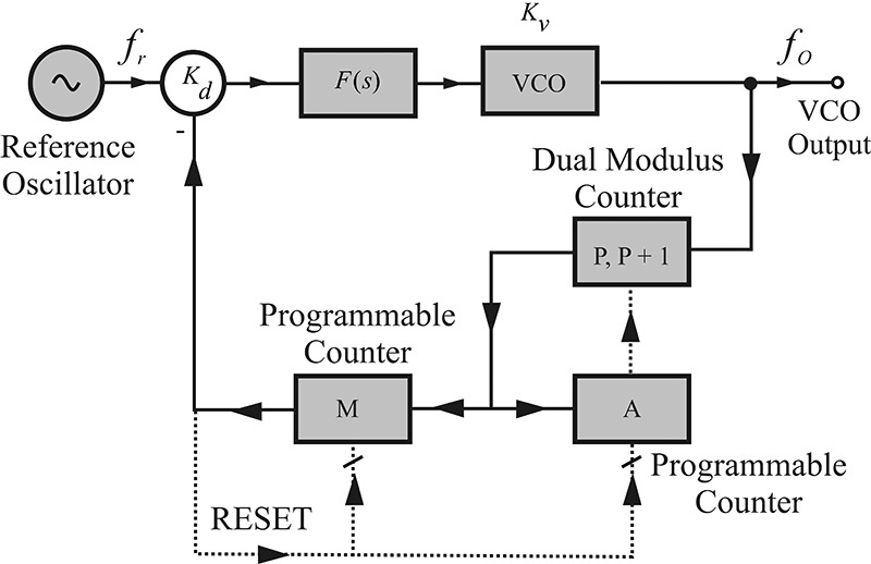
From Figure 11.17, the VCO frequency divided by P + 1 is concurrently applied to the input of the A- and M-counters. When the A-counter completes A times of division, the A-counter generates the control signal (usually the rising edge occurring after counting is completed); the division ratio of the dual modulus counter is then set to P and no further division is performed in the A-counter. Thereafter, only the M-counter operates. Thus, for the rest of VCO cycle, the VCO frequency divided by P is the input to the M-counter, which then divides the input (M - A) times. Similarly, the M-counter generates the “RESET” control signal when the division is completed and the M- and A-counters and the dual modulus counter return to their original states by the “RESET” control signal. After this, the operation explained above is repeated. As a result, the frequency of the VCO is divided by N = (M- A)P + A(P + 1). That is, after N cycles of VCO output, one period of the square wave is generated. Therefore, the frequency divider then divides the VCO output frequency by an arbitrary integer N.
A fractional frequency divider can be configured by adding some structures to the architecture of the integer frequency divider shown in Figure 11.17. That is, when the division ratio is changed to N = 100, 100, 100, 101, it corresponds to an average division of 100.25. As a generalization, suppose that, among total F cycles, a signal frequency is divided by N + 1 for K cycles and then divided by N for the remaining (F - K) cycles. The average division ratio M* becomes,
which gives the same effect as dividing the signal frequency by a fraction. It should be noted that the integer K is less than F. The average frequency of the divided output obtained by this division is obviously equal to the VCO frequency divided by M*, but the instantaneous frequency varies with time. The reason for implementing the fractional frequency divider in this way is that the frequency divider basically cannot perform fractional division and only integer division is possible. Thus, denoting the comparison frequency as fr, the synthesized output frequency of the VCO fo can be expressed in Equation (11.20).

The implementation of Equation (11.12) depends on the periodic implementation of N + 1. Increasing the division ratio from N to N + 1 is done by increasing the division ratio of the A-counter by 1 from Equation (11.19). In addition, the periodic increment of the A-counter by 1 is accomplished by connecting the output of the M-counter (after the VCO input is divided by N or an N + 1 rising edge is generated) to the input of a separate counter (accumulator), which is made to generate K carries in F cycles. The carries then periodically increase the division ratio of the A-counter by 1. As described above, the implementation of 100,100,100,101 is done by implementing the accumulator as a 2-bit counter. The 2-bit counter generates a carry as
0, 1, 2, 3↑0, 1, 2, 3↑... (1 carry is generated every 4 cycles)
When overflow occurs, the carry is generated. By passing it on to the A-counter, the A-counter is incremented by 1. Therefore, because the carry generation is accomplished with the accumulation of the rising edge outputs of the M-counter, the 2-bit counter is called the accumulator. The detailed architecture of the accumulator can be found in commercial application notes.1
1. Texas Instruments, Fractional/Integer-N PLL Basics, SWRA029, August 1999. Available online at www.ti.com/lit/an/swra029/swra029.pdf.
From the phase noise point of view, implementing the division ratio as a fraction has several advantages. First, it is not necessary to set the comparison frequency to be equal to the frequency step of the frequency synthesizer; the comparison frequency can be set to a higher frequency; for example, to make a frequency synthesizer of 890 MHz with a frequency step of 50 kHz using an integer divider, the comparison frequency must be fr = 50 kHz. Thus, the division ratio becomes N = 890/0.05 = 17,800. In contrast, for F = 16, the comparison frequency fr = 50 × 16 = 800 kHz and the division ratio NF becomes

In addition, note that the ratio between the integer and the fractional divider is N/NF = 16. Due to the lowering of the division ratio by 20log(16) = 24 dB, the effect of the phase detector noise floor can be reduced by 24 dB according to Equation (11.18), assuming the noise floor of the phase detector is constant irrespective of the comparison frequency. Thus, the fractional frequency divider eliminates the need to divide the VCO frequency by a large number N and the phase detector noise floor contribution is significantly reduced. As a result, the phase detector noise floor may not be considered in the output phase noise of the frequency synthesizer. Also, because the comparison frequency is high, the loop filter bandwidth of the PLL can be made wider, giving the advantage of a faster lock time.
A 900-MHz frequency synthesizer with a frequency step of 50 kHz must be configured using the 10-MHz reference oscillator given in Example 11.6. Compare the output phase noises of two frequency synthesizers: one uses the integer frequency divider and the other uses the fractional frequency divider with Fraction = 16.
Solution
The phase noises of the reference oscillator and VCO at the comparison frequency of 800 kHz (16 × 50 kHz) in the fractional frequency synthesizer can be computed in the same way as in Example 11.6. In addition, the noise floor of the phase detector at 800 kHz is similarly computed. This is shown in Table 11E.7, where the optimum loop bandwidth of the fractional frequency synthesizer appears to be between 1–10 kHz. The phase noise of the VCO at a frequency of 800 kHz is also calculated and is shown in the sixth column of Table 11E.7. By using the computed results, the phase noise of the fractional frequency synthesizer at 900 MHz is given in the last column.

N and K of the fractional frequency synthesizer can now be determined. Since
then N = 1125 and K = 0. However, note that the frequency step becomes 0.8 MHz/16 = 0.05 MHz because F = 16. Thus, the frequency synthesizer can increase the frequency by a frequency step of 0.05 MHz (i.e., 50 kHz) when K is increased successively. The comparison of the phase noise of the fractional synthesizer with that of the integer frequency synthesizer in Example 11.6 is shown in Figure 11E.4. The phase noise of the fractional frequency synthesizer shows an improvement by approximately 10 dB in the offset frequency range of 10 Hz–1 kHz. The improvement is due to the reduced contribution of the phase detector noise floor compared with the integer frequency synthesizer.

Figure 11E.4 Comparison of the phase noises of the fractional and integer frequency synthesizers. The fractional synthesizer provides a lower phase noise floor inside the loop bandwidth.
11.4 Loop Filters
11.4.1 Loop Filter
A loop filter, unlike other components used in a PLL, determines the overall operation and characteristics of the PLL. Therefore, it is necessary to discuss the loop filter by considering the PLL’s characteristics rather than by discussing the loop filter as a component. The loop filters are classified based on their component types and on the loop filters’ transfer functions because those filters directly affect the transfer function of a PLL.
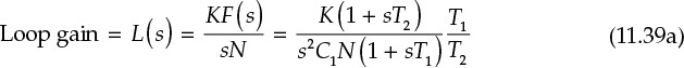
The architecture of a PLL is shown again in Figure 11.18. In that figure, because the PLL is structured as a feedback, it can be analyzed based on open-loop gain (simply referred to as loop gain). Denoting the transfer function of the loop filter by F(s), the open-loop gain L(s) is obtained as with Equation (11.21).

Note that F(s) has the highest order of sm+n–1 in the denominator because the VCO contributes 1/s to the denominator.
In addition, using the open-loop gain, the closed-loop gain can be expressed as Equation (11.22).

The classification of the loop filter is based on the highest order of the denominator of L(s), which is defined as the order of the loop filter. Therefore, for Equation (11.21), the order of the loop filter is m + n. In addition, even when the phase detector is directly connected to the VCO without the loop filter (in this case, F(s) = 1), the open-loop gain will have a term of s-1 due to the transfer function of the VCO. Thus, the order of the loop filter becomes a first order even when there is no loop filter in the PLL. Also, when a low-pass filter whose transfer function has a first-order denominator is included in the PLL, the order of the loop filter becomes a second order. The definition of the order may be different in other literature if the order is defined as the order of a loop filter alone.
In addition, the integration factor in Equation (11.21) is critical in determining the characteristics of the PLL, and its number is often used in the classification of loop filters. This is called the type of the loop filter. Equation (11.21) has the term sm in the denominator and the loop filter is thus referred to as type m. That is, the type indicates the number of ideal integrators included in the transfer function. The closed-loop gain H(s) of the PLL configuration in Figure 11.19 for a first-order loop filter is expressed as


Figure 11.19 Responses of the first-order loop filter: (a) frequency response and (b) tracking for a step phase change
Therefore, from Equation (11.23), the 3-dB bandwidth (the frequency at which the magnitude of the open-loop gain is 1/2½) is K/N. As a result, the loop bandwidth is K/N.
When a step phase change (θi = Δθru(t)) is applied to the input with the closed-loop transfer function in Equation (11.23), the output phase is

The inverse of the Laplace transform in Equation (11.24) can be written as

From Equation (11.25), the output phase at the steady state can be seen to be NΔθr for a step phase change of Δθr. Also note that the output frequency for a step frequency change follows the form of Equation (11.24) as expressed by Equation (11.26).
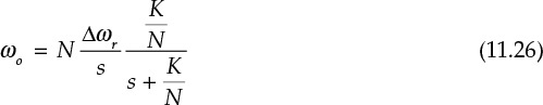
Thus, the output frequency tracks the step input frequency change as the output phase follows the step phase change. Figure 11.19 shows a first-order PLL frequency response and the output waveform for a step phase change.
Note that the phase detector output generates an error given by Equation (11.5) for tracking the step frequency change; however, the output frequency tracks the step frequency change without error. In the first-order PLL, the output is able to track the input frequency change that accompanies the phase error. In addition, as we saw in the previous explanation of phase detectors, not only the DC phase detector voltage, but also many of the comparison frequency’s harmonic components are present in the actual phase detector output. Since the first-order loop filter applies the phase detector output to the VCO without filtering the harmonics, many frequency-modulated spurious components appear at the VCO’s output due to those harmonics. Therefore, the first-order PLL is not commonly used due to its inability to remove the harmonics rather than because of the phase error problem.
11.4.2 Second-Order Loop Filters
The phase error and spurious components of the first-order PLL can, to some extent, be removed by configuring the PLL using a second-order loop filter. In order to remove the phase error, it is necessary to insert an integrator into the loop filter as previously explained. The second-order loop filter can be constructed by inserting an integrator in a first-order loop filter. The second-order loop filter transfer function can be expressed as

The first term in Equation (11.27) is the integration of the input and the second term is proportional to the input. Substituting Equation (11.27) into Equation (11.21), the open-loop gain can be obtained with Equation (11.28).

Thus, the closed-loop gain H(s) is obtained as expressed in Equation (11.29).
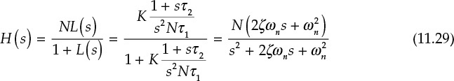
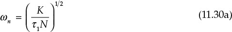
Here, ωn and ζ are called the natural frequency and damping ratio, respectively, of the second-order transfer function, and ωn and ζ are defined in Equations (11.30a) and (11.30b).

As s → 0, H(s) approaches N, and H(s) → 0, for s → ∞. Thus, the closed-loop gain H(s) has the frequency response of a low-pass filter. Its frequency response is shown in Figure 11.20 with ζ as a parameter. The bandwidth is approximately ωn, which varies slightly according to ζ. Calculating the 3-dB bandwidth results in Equation (11.31).

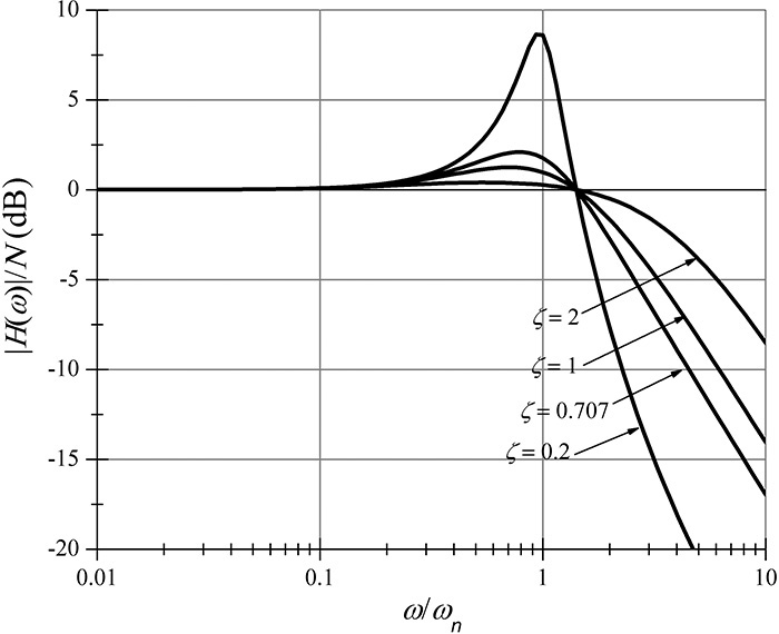
From Equation (11.31), the loop bandwidth is close to the natural frequency and varies according to the damping ratio ζ. Therefore, the approximate loop bandwidth can be considered the natural frequency. From Equation (11.28), the magnitude of the open-loop gain L(s) at the natural frequency ωn can be approximated as 1 by ignoring the term sτ2, which is generally small at ωn. Therefore, the natural frequency ωn is the frequency at which the magnitude of the open-loop gain becomes approximately 1.
Using the transfer function of Equation (11.29), the output phase for a step phase change is found to be

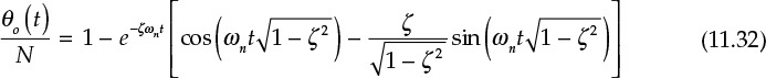
and θo(t) can be obtained from an inverse Laplace transform expressed in Equation (11.32).
The time response θo(t) is shown in Figure 11.21 with ζ as a parameter. Note that Equation (11.32) is the output phase change due to the step phase change, but as explained previously, the output phase change can be interpreted as the output frequency change for a step frequency change (ωi = Δωru(t)). The same response will be obtained for the output frequency ωo(t) for a step frequency change ωi = Δωru(t).
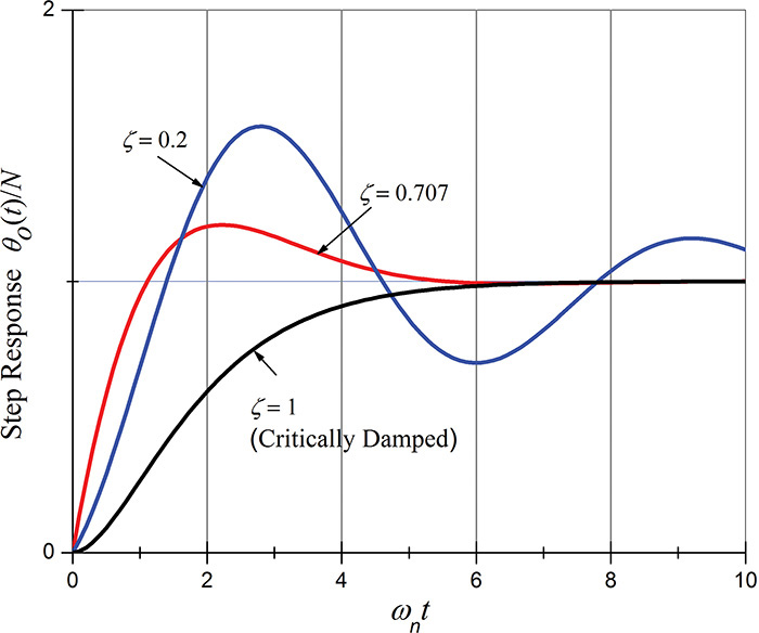
From Figure 11.21, at the steady state, the output phase tracks a step phase change that is irrespective of the damping ratio ζ. Thus, the output phase should track the input change as quickly as possible without overshooting it. From Figure 11.21, the optimal tracking can be observed for ζ = 0.707. The time taken to reach the steady state is known as the lock time. The lock time is defined as the time typically taken to reach within 5% of the steady state’s value. The lock time usually varies depending on ζ, but for ζ = 0.707, Equation (11.33) gives

Here ωn = 2πfn. Note that in the case of the second-order loop filter, due to the role of the integrator, the phase and the frequency track the input without phase errors for a step frequency change. Therefore, beyond the second order, because the VCO tracks the phase and frequency of the reference oscillator without error, the VCO can be viewed as a phase lock state in the truest sense.
From the results of the second-order loop filter described above, the loop bandwidth is approximately the natural frequency ωn and the optimal tracking for a step change can be achieved by selecting ζ = 0.707. The lock time thus obtained is the same as that given by Equation (11.33). As a result, the narrower the loop bandwidth ωn, the longer the lock time, whereas the wider the loop bandwidth ωn, the faster the lock time. Therefore, once the loop bandwidth is determined in the second-order loop filter PLL, the optimal lock time can be automatically determined. However, in order to make the lock time faster, the loop bandwidth cannot be set to be infinitely large. The loop bandwidth should be set to be less than the comparison frequency. If the loop bandwidth is greater than the comparison frequency, the equations previously derived will not hold. In the derivation, the phase detector output was assumed to be DC. However, in such a case, the loop filter is unable to sufficiently filter out the harmonics of the phase detector and, just as in the first-order loop filter, the harmonics of the comparison frequencies are transferred directly to the VCO. The phase detector output waveform will then severely frequency-modulate a VCO frequency, which gives rise to many unwanted spurious characteristics.
11.4.3 Implementation of a Second-Order Loop Filter
The circuit implementations of the second-order loop filter described above are shown in Figure 11.22. The circuit in Figure 11.22(a) is a second-order loop filter for the phase detector with a charge pump and the circuits in Figures 11.22(b) and 11.22(c) are the active and passive loop filters for the voltage output phase detector.

Figure 11.22 Second-order loop filters: (a) loop filter for the charge pump phase detector output and loop filters for the voltage phase detector output; (b) active and (c) passive loop filters
The loop gain of Figure 11.22(a) is expressed in Equation (11.34).

Thus, the ideal second-order transfer function can be implemented using only passive components. Also note that the transfer function of the loop filter F(s) is the impedance Z(s). In the case of Figure 11.22(b), assuming an ideal operational amplifier, Equation (11.35) gives us,

which also implements an ideal second-order transfer function. Since F(s) has a voltage–voltage relationship, the loop filter in Figure 11.22(b) can be applied to the voltage–output phase detector without a charge pump. In addition, because the loop filter uses an active device, it is called an active loop filter. In the case of Figure 11.22(c), F(s) is expressed in Equation (11.36)

and can be used as an approximate second-order loop filter.
11.4.4 Measurement of a PLL
The characteristics of a PLL frequency synthesizer include phase noise, spurious characteristics, and the transient response for a unit step frequency change. The phase noise and spurious characteristics can be measured with a spectrum analyzer and the transient response for a unit step change can be measured with an oscilloscope or signal analyzer.
The spurious characteristics can be obtained by measuring the output spectrum of the VCO with the spectrum analyzer, as shown in Figure 11.23. To measure phase noise, a spectrum analyzer is used, as explained in Chapter 10. When the phase noise utility is installed in the spectrum analyzer, the phase noise can be conveniently measured without the computation of the N/C ratio as described in that chapter.

Figure 11.23 Measurement of a frequency synthesizer. The spectrum analyzer is used to measure the phase noise of a PLL and the oscilloscope is used to measure the tracking response.
The unit step transient response can be obtained by measuring the tuning voltage Vc of the VCO with an oscilloscope, as shown in Figure 11.23. However, the tuning voltage is not a direct measurement of the VCO’s frequency even though it is proportional to the VCO’s frequency. The instrument that can directly measure the frequency change is the signal analyzer or modulation analyzer.2 Alternatively, the frequency change with respect to time can be measured by setting the spectrum analyzer SPAN to 0 Hz, as shown in Figure 11.23, and applying the trigger pulse that is synchronized to the unit step frequency change and to the external trigger input in the spectrum analyzer. With these settings, the spectrum analyzer shows the input power variation within the RBW (resolution bandwidth) of the specified center frequency versus time. Consequently, the measurement shows the frequency of the VCO with time and the lock time can be obtained by measuring the time taken to reach the steady-state frequency with an error of the RBW.
2. Agilent Technologies, E5052A Signal Source Analyzer, Advanced Phase noise and Transient Measurement Techniques, Application Note 5989-1617EN, October 2004.
Some examples of measurement results for a frequency synthesizer are shown in Figure 11.24. The output phase noise of the frequency synthesizer and the transient frequency response for a unit step frequency change are shown in Figures 11.24(a) and 11.24(b), respectively. As expected, the output phase noise tracks the phase noise of the VCO outside the loop bandwidth, whereas it follows the phase noise of the reference oscillator within the loop bandwidth. In Figure 11.24(a), the phase noise approximated by two straight lines can be seen to intersect at about 15 kHz and the loop bandwidth can be estimated to be about 15 kHz. Figure 11.24(b) shows the time response to a unit step frequency change. This is measured using a modulation analyzer; the lock time in the figure can be seen to be about 500 μsec.

Figure 11.24 (a) Measured phase noise of the phase-locked VCO and (b) lock time for a frequency jump from 865 to 915 MHz. The PLL parameters are reference frequency fref = 200 kHz, fo = 900 MHz, N = 4500, Kv = 2π × 20 (Mrad/V), and Kd = 5 mA/(2π) (rad/V). The loop filter order is fourth and its loop bandwidth = 20 kHz, and phase margin is φp = 45°.The lock time is about 153 μsec. Source: National Semiconductor Application Note 1001, An Analysis and Performance Evaluation of a Passive Filter Design Technique for Charge Pump PLL’s, July 2001.
Next, Figure 11.25 shows the spectrum of the frequency synthesizer measured by expanding the SPAN of the spectrum analyzer. The SPAN is set wider than the comparison frequency. Spurious characteristics can be seen to occur in addition to the synthesized frequency components. As mentioned earlier, the phase detector includes many harmonic components of the comparison frequency. The loop filter removes these harmonics to some extent, but when the filtering is not sufficient, the remaining harmonics modulate the VCO and spurs occur.

Figure 11.25 Spurs in the frequency synthesizer. The loop filter in Figure 11.24 is used. The spur level is measured to be about 74.7 dBc. Source: National Semiconductor Application Note 1001, An Analysis and Performance Evaluation of a Passive Filter Design Technique for Charge Pump PLL’s, July 2001.
To see these effects, by denoting the leakage voltage of the comparison frequency harmonics at the output of the loop filter as Vssin(ωmt), the VCO is FM modulated by this leakage voltage. This can be expressed with Equation (11.37).

In addition to the synthesized frequency, the output, the two frequency components ωc + ωm and ωc – ωm from the right-hand term of Equation (11.37) appear. Thus, spurs occur as shown in Figure 11.25 and it is necessary to lower the spur level by narrowing the loop filter. In the case where a fast lock time is required, the bandwidth should be set wider and the loop filter is then unable to sufficiently attenuate the comparison frequency harmonics appearing at the phase detector’s output. Consequently, this results in larger spurs at the VCO’s output. However, when the bandwidth is overly reduced so as to suppress the spurs, the lock time becomes longer. Higher-order loop filters may be used in such a situation.
11.4.5 Higher-Order Loop Filters
The second-order loop filter can track the frequency and phase of the reference oscillator, and it can be used as a basic loop filter for PLL configuration. However, when spurs are above the specified level, the second-order loop filter does not provide an alternative way to suppress spurs other than to narrow the loop bandwidth at the expense of the lock time. To some extent, the problems that arise between the lock time and the spurs can be solved by using a higher-order loop filter.
Note that a higher-order loop filter yields the transfer function of an open-loop gain that is higher than a third order. Generally, the PLL can become unstable for the open-loop gain transfer function with the third order and above. One way of resolving the PLL instability is to provide a phase margin or gain margin in the open-loop gain. The phase margin method is commonly used in a PLL. The design of higher-order loop filters depends in part on the type of the loop filter. In this section, we will discuss a design that is limited to a charge pump PLL loop filter. The higher-order loop filters are shown in Figure 11.26 and they are formed by modifying the second-order loop filters to give more attenuation at the comparison frequency harmonics. Figure 11.26(a) shows a third-order loop filter and Figure 11.26(b) shows a fourth-order loop filter.

Figure 11.26 Circuit implementation of charge pump loop filters: (a) the third order and (b) the fourth order
In Figure 11.26(a), R2 and C2 comprise the second-order loop filter. The impedance Z(s) of R2-C2 branch is expressed in Equation (11.38).

At lower frequencies, the impedance Z(s) is approximated by 1/sC2, which decreases as the frequency increases. However, at higher frequencies, the impedance becomes Z(s) ≅ R2. Thus, there is no attenuation of the harmonic leakage for a frequency higher than fc = 1/2πR2C2. By adding C1 in parallel to the R2-C2 branch, the harmonic leakage of higher frequency can be attenuated due to C1. For the fourth-order loop filter in Figure 11.26(b), an R3-C3 stage is added to the third-order loop filter. The R3-C3 stage has no effect at low frequency. However, at high frequency the R3-C3 stage functions as a low-pass filter thereby severely attenuating the harmonic leakage of the phase detector output. Note that the values of C1 and C3 added in the higher-order loop filters are basically small and therefore have little or no effect on the basic form of the second-order loop filter within the loop bandwidth. However, they are inserted to give more harmonics attenuation outside the loop bandwidth. Thus, within the loop bandwidth, the added components in the third-order and fourth-order loop filters have minimum effect on the basic form of the second-order loop filter; this effect appears outside the loop bandwidth and attenuates the high-frequency harmonic leakage of the phase detector output. In reality, however, the added components somewhat distort the response of the second-order loop filter and the effects of the added components must be taken into account when determining their values.
When the third-order loop filter in Figure 11.26(a) is used in the PLL with the integer frequency divider shown in Figure 11.18, the loop gain L(s) is expressed in Equations (11.39a)–(11.39c).
Therefore, the frequency response characteristics can be computed using Equation (11.40).
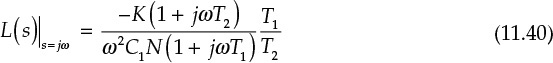
Generally, the phase of L(s) increases from -180° and then tends to decrease again as the frequency increases, as shown in Figure 11.27. Therefore, for stability, the loop gain must be 1 at the point where the phase is maximum, which then gives the maximum phase margin. The phase from Equation (11.40) is

Differentiating Equation (11.41) to obtain the frequency ωp at which φ(ω) is maximum, we obtain Equation (11.42).

Then, the frequency for the maximum phase margin ωp is given by

The frequency ωp can be defined as the loop bandwidth. This definition is somewhat different from that of the loop bandwidth ω3dB of the second-order loop filter, but it can be used to identify a newly defined loop bandwidth.
From Equation (11.43), T2 can be expressed in terms of ωp and T1 with Equation (11.44).

Denoting the phase margin as φp, the phase margin from Equation (11.41) is φp = φ (ωp) + 180°. Thus, substituting the result of Equation (11.44) into Equation (11.41), T1 can be obtained with Equation (11.45).

Then, once the loop bandwidth ωp and phase margin φp have been defined, the time constants T1 and T2 can be calculated from Equations (11.44) and (11.45).
In addition, in order to make φp of Equation (11.45) equal to the phase margin, for the determined T1 and T2, |L(jωp)| = 1. Thus,
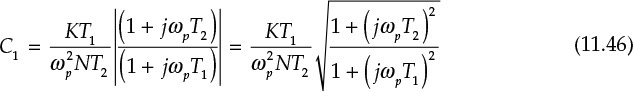
Since ωp, T1, and T2 have already been determined, the value of C1 can be calculated using Equation (11.46), from which R2 and C2 can be determined using Equations (11.39b) and (11.39c), and expressed in Equations (11.47) and (11.48).


In summary, for the given loop bandwidth ωp and phase margin φp, the two time constants T1 and T2 can be calculated with Equations (11.44) and (11.45). As a result, all the element values of the third-order PLL loop filter can be determined. The lock time of the third-order loop filter is similar to that of the second-order loop filter, and Tlock ~ 1/ fp (ωp = 2πfp).
The design of a frequency synthesizer of fo = 900 MHz requires the use of a third-order loop filter. The third-order loop filter must have a loop bandwidth of ωp = 2π × 10 kHz and a phase margin of φp = 45°. The comparison (or reference) frequency is fref = 200 kHz. The tuning sensitivity of VCO is Kv = (2π) × 20 Mrad/V. The phase detector constant is Kp = 5/(2π) mA/rad. Compute the element values of the third-order loop filter.
Solution
From the given values,
By substituting the values of the loop bandwidth and phase margin into Equation (11.45),

Substituting the N and time constants T1 and T2 calculated above in Equation (11.46),

Using the value of C1 and substituting C1 into Equations (11.47) and (11.48), the third-order loop filter element values can be obtained as shown in Figure 11E.5.


Substituting the calculated values into Equation (11.40), the frequency response of L(s) can be computed and is shown in Figure 11E.5. In that figure, when the loop gain is 0 dB (i.e., the loop gain = 1), the phase is -135°, which is away from -180° by 45° and the phase margin can be seen to be 45°.
For the parameters of the PLL given in Example 11.9, compute the third-order loop filter values using the equations in the ADS display window and graph its Bode plot for a frequency range of 10 Hz–10 MHz.
Solution
The PLL design in Example 11.9 occurs frequently in PLL design and requires only simple computations using a conventional calculator. This series of computations can be solved using the ADS display window without a calculator. Similar programs are available from the Web sites of PLL IC vendors.3
3. Refer to the Web site of Analog Devices at www.analog.com.
First, enter the equations that define the PLL parameters shown in Measurement Expression 11E.1 in the display window.
![]() Kv=20 M
Kv=20 M ![]() Kp=5m
Kp=5m ![]() fref=200k
fref=200k ![]() fo=900 M
fo=900 M ![]() fp=10k
fp=10k
![]() phi=45*pi/180
phi=45*pi/180
![]() N=fo/fref
N=fo/fref ![]() wp=2*pi*fp
wp=2*pi*fp ![]() K=Kv*Kp
K=Kv*Kp
Measurement Expression 11E.1 Definition of the PLL parameters in the display window
Note that expressions such as 20e6 and 5e-3 are not required and they can be stated using prefixes such as m, k, M, G, and so on. Next, determine the plot frequency range, which can be written as follows in Measurement Expression 11E.2:
![]() fstart=10
fstart=10 ![]() fstop=10M
fstop=10M ![]() n=20
n=20 ![]() Dec=log(fstop/fstart)
Dec=log(fstop/fstart)
![]() x=generate(0, Dec,n*Dec)
x=generate(0, Dec,n*Dec) ![]() f=fstart*10**(x)
f=fstart*10**(x) ![]() w=2*pi*f
w=2*pi*f ![]() s=j*w
s=j*w
Measurement Expression 11E.2 Definition of the parameters for the Bode plot in the display window
Here, n sets the number of the computing points per decade of frequency change. The variable Dec is the decade number of the frequency range set by fstart and fstop, and thus n*Dec number of points are computed. The function generate() generates a sequence from 0 to Dec with points given by n*Dec.
The two sets of equations given above are commonly required in PLL loop filter design. Now, the third-order loop filter values can be computed using the equations derived from Equations (11.44) to (11.48) and can be written as follows in Measurement Expression 11E.3:
![]() T1=(1/cos(phi)-tan(phi))/wp
T1=(1/cos(phi)-tan(phi))/wp ![]() T2=1/(wp**2*T1)
T2=1/(wp**2*T1)
![]() C1=K*T1/(wp**2*N*T2)*sqrt((1+(wp*T2)**2)/(1+(wp*T1)**2))
C1=K*T1/(wp**2*N*T2)*sqrt((1+(wp*T2)**2)/(1+(wp*T1)**2))
![]() C2=C1*(T2/T1-1)
C2=C1*(T2/T1-1) ![]() R2=T2/C2
R2=T2/C2
![]() L3=K*(1+s*T2)/(s**2*N*(C1+C2))*(1+s*T1))
L3=K*(1+s*T2)/(s**2*N*(C1+C2))*(1+s*T1))
Measurement Expression 11E.3 Loop filter element values and transfer function in the display window
The last equation is for the Bode plot. Using the listing column in ADS, the computed values can be found as
C1 = 2.332 nF, C2 = 11.26 nF, and R2 = 3.413 kΩ
These values are the same as those calculated in Example 11.9. In addition, the Bode plot of the open-loop gain L3 with the calculated values can be obtained as shown in Figure 11E.6. From Figure 11E.6, the determined third-order loop filter yields the exact desired loop bandwidth (where the loop gain is 1) and phase margin of 10 kHz and 45°, respectively.

Figure 11E.6 Frequency response of the open-loop gain of the third-order loop filter with the calculated element values
With the loop filter thus configured, it is not possible to know absolutely the magnitudes of the spurs. However, they are more attenuated than in the case of the second-order loop filter and the relative degree of their attenuation can be determined by comparing the open-loop gain with that of the second-order loop filter. When the spurs of the configured third-order loop filter are measured and are still found to be greater than the specifications shown in Figure 11.25, the spurs’ performance can be improved by employing a fourth-order loop filter, which is an extension of the third-order loop filter. In Figure 11.25, in order to make the spurs below the phase noise, an attenuation of approximately 10 dB is required. The 10-dB attenuation can be achieved by extending the third-order loop filter to the fourth-order loop filter in Figure 11.26(b). The transfer function of the additional R3-C3 stage is expressed in Equation (11.49).

Therefore, the required attenuation of the spurs at the comparison frequency fref, ATTN can be defined with Equation (11.50).
Using Equation (11.50), the time constant T3 can be calculated using Equation (11.51).

Adding R3-C3 to the third-order loop filter causes a slight change in its element values. The loop gain of the fourth-order loop filter can be approximately written as Equation (11.52).

Here, the time constants T1 and T2 are the same as those in Equations (11.39b) and (11.39c). This is similar to the transfer function of the third-order loop filter given by Equation (11.39a). Therefore, Equation (11.44) can be rewritten as Equation (11.53)

and the relationship between the loop bandwidth and phase margin is obtained with Equation (11.54.)

Thus, T3, T1, and T2 can be determined from Equations (11.51), (11.53), and (11.54). The calculated values T1, T2, and T3 can be substituted into L(s) of Equation (11.52). For the phase margin, |L(s)| must be equal to 1 at ωp. As in the third-order loop filter design, C1 can be obtained with Equation (11.55).

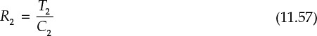
In addition, C2 and R2 can be calculated from the time-constant relationships using Equations (11.56) and (11.57).

Using these formulas, all the fourth-order loop filter element values can be determined. However, as T3 is expressed in terms of R3C3, there is a certain degree of freedom. The value of C3 should be set 10 times smaller than C1 because R3C3 must not affect C1. Thus, all the element values are accurately calculated, and the reader may refer to reference 3 at the end of this chapter for the exact values.
Using ADS, design the fourth-order loop filter for the PLL parameters given in Example 11.10, with an added parameter ATTN as
ATTN = 10 dB
Also, compare the open-loop gain of the fourth-order loop filter with that of the third-order loop filter.
Solution
The first two sets of equations in the ADS display window are the same as those in the third-order loop filter design. The difference is in computations for the element values. Using Equations (11.50)–(11.57), the equations for the element values can be written as follows in Measurement Expression 11E.4:
![]() ATTN=10
ATTN=10 ![]() T3=sqrt((10**(ATTN/10)-1)/(2*pi*fref)**2)
T3=sqrt((10**(ATTN/10)-1)/(2*pi*fref)**2)
![]() T1=(1/cos(phi)-tan(phi))/wp-T3
T1=(1/cos(phi)-tan(phi))/wp-T3 ![]() T2=1/(wp**2*T1)
T2=1/(wp**2*T1)
![]() C1=K*T1/(wp**2*N*T2)*sqrt((1+(wp*T2)**2)/(1+(wp*T1)**2))
C1=K*T1/(wp**2*N*T2)*sqrt((1+(wp*T2)**2)/(1+(wp*T1)**2))
![]() C2=C1*(T2/T1-1)
C2=C1*(T2/T1-1) ![]() R2=T2/C2
R2=T2/C2
![]() C3=C1/10
C3=C1/10 ![]() R3=T3/C3
R3=T3/C3
![]() L4=K*(1+s*T2)/(s**2*N*(C1+C2)*(1+s*T1)*(1+s*T3))
L4=K*(1+s*T2)/(s**2*N*(C1+C2)*(1+s*T1)*(1+s*T3))
Measurement Expression 11E.4 Loop filter element values and transfer function in the display window
Note that the open-loop gain L4 obtained with Equation (11.52) is not an exact one. The open-loop gain of the fourth-order loop filter is somewhat more complex than that given by Equation (11.52). In the computation of L4, the element values of C3 and R3 are not required; only the value of T3 is necessary. The value of C3 is set to C1/10 to make the effect of R3 - C3 branch small. The computed values of the elements are
C1 = 1.539 nF, C2 = 12.52 nF, R2 = 3.067 kohm, C3 = 0.153 nF, and R3 = 15.5 kohm
Figure 11E.7 shows the open-loop gain of the computed fourth-order loop filter. The open-loop gain magnitude is close to 0 dB and its phase margin is close to 45° at the loop bandwidth of 10 kHz. The Bode plot of the third-order loop filter open-loop gain is also included for comparison. The magnitude L4 should be lower than that of L3 by 10 dB at fref = 200 kHz. However, that difference is about 5 dB, which is smaller than 10 dB. The reason for the difference is because the loop filter calculation method relies on the previously explained approximation method. The method of finding exact values can be found in the end-of-chapter problems, or the programs that calculate the exact fourth-order loop filters are available on the Web sites of PLL IC vendors.

11.5 PLL Simulation in ADS
A PLL can be simulated using ADS. The synthesis of a loop filter by optimization and the simulation of the phase noise and transient response for a unit step frequency change is also possible in ADS; however, ADS cannot simulate the spurious characteristics. For that simulation, a mathematical model of the phase detector’s waveform at the steady state is required. The key factors of spur generation include the leakage current of the phase detector and the asymmetry of the charge pump current (see reference 3 at the end of this chapter). Currently, however, it is difficult to model these phenomena mathematically. As a result, accurately simulating the spur characteristics using ADS can be a problem. In this section, we will discuss loop filter synthesis and the simulation of phase noise and transient response in ADS.
As phase noise simulation is related to small-signal noise simulation, the phase noise simulation can be performed using an AC simulation, while the transient response requires an envelope simulation.
11.5.1 Loop Filter Synthesis
Examples of PLL simulation templates are in the DesignGuide of the ADS menu (DesignGuide/PLL). After the clicking the Menu command, the first pop-up window appears; then chose Select PLL Configuration. The second pop-up window for the PLL configuration will appear; in the Type of Configuration tab, choose Frequency Synthesizer and then select Loop Frequency Response in the Simulation tab. Next, choose Charge Pump in the Phase Detector tab and Passive 3 Pole in the Loop Filter tab. The design files named SYN_CP_FQ_P3P.dsn and SYN_CP_FQ_P3P.dds will be generated. Rename the generated design file as SYN_third. The design file contains three circuits: one for the closed-loop response, one for the open-loop gain, and one for the loop filter frequency response. Delete the two circuits for the closed-loop response and loop filter, and then modify the circuit as shown in Figure 11.28. There are two MeasEqns that are initially hidden. These can be shown by setting Parameter Visibility to Set All in the Component Options of the pop-up window.
Figure 11.28 Loop filter design using optimization. The voltage Vout_OL corresponds to the open-loop gain of the PLL. VAR2 sets the values of the PLL components and VAR4 sets the values of the loop filter. VAR5 defines the parameters for the PLL design objectives. The measurement equation meas1 computes the phase and magnitude of Vout_OL and defines the phase margin. Then, meas2 defines the variable names for the display window. In meas2, the defined variables that correspond to the closed-loop filter and the loop filter output voltages are deleted. Goals computes the values of the cost functions using the AC simulation result AC1. AC2 computes the frequency response of the open-loop gain for the frequencies given by SwpPlan1 when the optimization finishes.
In Figure 11.28, LinearPFD is a subcircuit built with a voltage-controlled current source (VCCS). The LinearPFD models the charge pump PFD explained in the previous section, which generates the current in proportion to the phase difference. Here, the phase difference is given by the voltage source. The LinearVCO is an integrator that is similarly modeled using two controlled sources. The LinearDivider also models the frequency divider using a VCVS (voltage-controlled voltage source). The previously mentioned component values of PLL are defined in VAR2. The element values of the loop filter are defined in VAR4.
In VAR5, the variable UnityGainFreq represents the loop bandwidth where the open-loop gain is 1. The variables Min_Phase_Margin and Max_Phase_Margin define the allowable values for the phase margin in optimization. The original schematic does not include the group delay. In that case, the phase of the open-loop gain may not be optimized at the phase peak frequency, which we do not want. Since the group delay is equal to 0 at the phase peak frequency, the allowable group delay limit is set using the variable GD_Limit, which is then used in Goal1 to optimize the group delay to 0. The meas1 defines the open-loop gain, phase margin, and group delay necessary for optimization. The meas2 is a declaration of the output variable for the display window. The original schematic includes more variables but they are deleted for simplification.
The goals from Goal1 to Goal3 are connected to the AC simulation AC1. The AC1 is modified to simulate three frequencies, from UnityGainFreq-Deltaf to UnityGainFreq+Deltaf. This is necessary to compute the group delay. The group delay GD defines the phase change with respect to frequency. Then, the loop filter can be designed using optimization to minimize the three goals. The optimization control Optim1 optimizes the loop filter element values to fit the goals. The AC simulation AC2 is not connected to the goals and it is used to compute the Bode plot of the open-loop gain after the optimization. The sweep frequency range of AC2 is specified in SwpPlan1. After the optimization finished, the Optim1 computes the Bode plot using AC2.
First, the loop filter element values are optimized for a 10-kHz loop bandwidth and a 45° phase margin using the PLL parameters given in Example 11.10. The phase margin is set to the range 45°– 46°. The OLgain is set to the range 0.99–1.01. The group delay GD is set to close to 0. The optimized element values are compared in Table 11.2.

Figure 11.29 shows the magnitude and phase of the optimized open-loop gain. The phase margin is close to 45° and the open-loop gain is close to 1 at the frequency of the 10-kHz loop bandwidth. The higher-order loop filter, such as the fourth-order loop filter, can be obtained using a similar optimization procedure.
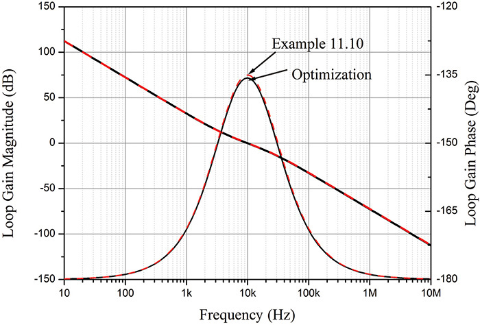
Figure 11.29 Comparison of the optimized open-loop gain with that computed in Example 11.10. The phase margin is close to 45° at 10 KHz and the difference is below 1°.
11.5.2 Phase Noise Simulation
The PLL phase noise simulation shown in Figure 11.30 can be set by selecting a PLL from the DesignGuide. Then, modify the loop filter as shown in Figure 11.30.

Figure 11.30 Phase noise simulation. In the simulation, voltages represent the phases of PLL components and the circuit is simulated using voltages. Reference oscillator is a noise voltage source whose spectrum is specified by the user as shown in the schematic. The component Charge_Pump generates the output current proportional to the difference of the two input voltages. The VCO produces the output voltage’s integrating input current and then the spectral noise voltage is added. LinearDivider is modeled using a VCVS (voltage-controlled voltage source).
In order to compare the results of Example 11.1 with the ADS simulation, the loop filter is set to be a second-order loop filter, as shown in Figure 11.30. The values of C1 and R1 of the second-order loop filter can be determined using the given fn = 1 kHz and fn = 10 kHz, and the damping ratio ζ = 0.707. From Equations (11.30a) and (11.30b), τ1 and τ2 can be determined as
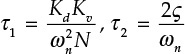
and from the values of τ1 and τ2, C1 and R1 can be computed as
The values of C1 and R1 are computed using the equation in ADS.
Then, since the noise floor of the frequency divider and phase detector were not considered in Example 11.1, a frequency divider and a phase detector without the noise floor should be selected. However, the phase detector without the noise floor is not available in ADS and thus the noise current is set to 0 to eliminate the effect of the noise floor. The frequency divider without the noise floor is available in ADS and the frequency divider is replaced with the new frequency divider in the default PLL simulation schematic. Next, it is necessary to input the phase noises of the reference oscillator and VCO. Instead of a tabular form, the phase noise requires an input as shown in Figure 11.30 that is represented by the 30 dB, 20 dB, and 10 dB slopes, and the noise floor. The phase noise values in Table 11E.1 are thus entered as shown in Figure 11.30.
The simulated phase noise is shown in Figure 11.31. The phase noise simulation results with respect to the loop bandwidth change are the same as those in Example 11.1. The phase noises of the VCO and reference oscillator multiplied by 1000 are also shown in Figure 11.31. These correspond, respectively, to PNTotal, PN_VCO_FreeRun, and PN_RefChain_FreeRun of that figure. They are calculated in the display window using the following equations in Measurement Expression 11.1:
![]() PN_VCO_FreeRun=10*log(0.5*VCO_FR.noise**2)
PN_VCO_FreeRun=10*log(0.5*VCO_FR.noise**2)
![]() PN_RefChain_FreeRun=10*log(0.5*RefChain.noise**2)
PN_RefChain_FreeRun=10*log(0.5*RefChain.noise**2)
![]() PNTotal=10*log(0.5*VCOout.noise**2)
PNTotal=10*log(0.5*VCOout.noise**2)
Measurement Expression 11.1 Definitions of phase noises in the display window
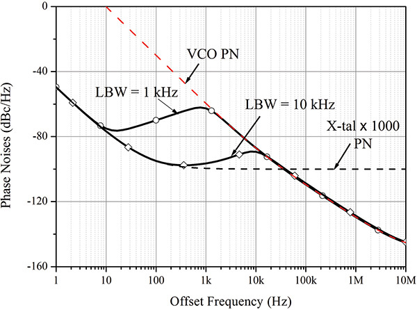
The calculated values in Figure 11.30 are the voltage values of the noise with respect to frequency. Note that because the simulation gives the noise simulation results, all the noise voltage variables in the previous equations have the noise extension. Of the computed noise voltages, VCO_FR.noise is not explicitly specified in the simulation schematic of Figure 11.30, but it is the value automatically calculated by the subcircuit VCO and stored in the dataset as VCO_FR.noise.
11.5.3 Transient Response Simulation
The simulation of a PLL’s transient response can be performed by selecting the ADS DesignGuide menu and then Transient Response Simulation in the pop-up window that appears. Also, in the course of selecting the loop filter, Passive 3 Pole must also be selected for the transient simulation. This automatically generates the default schematic window for the transient response simulation shown in Figure 11.32. In the autogenerated circuit, the loop filter is configured as shown in Figure 11.32. The loop filter element values in the schematic window are replaced by those of the third-order loop filter of Example 11.9: Kv, Kd, N, and the comparison frequency fref, which correspond to Kv, Id, N0, and Fref in Figure 11.32.

Figure 11.32 Transient response simulation. The terminal VCO is the undivided VCO output and the terminal freq outputs the undivided frequency values. The terminal vcon is the divided-by-(N + dN) output.
In that figure, it is necessary to understand the two components, VCO_DivideByN and PhaseFrequencyDetCP in order to be able to simulate the PLL’s transient response. PhaseFrequencyDetCP is the PFD with the charge pump explained earlier, and its input signal becomes the baseband signal, which is a time-varying waveform without a carrier. In Figure 11.32, the reference signal is set using a DC power supply and is made to vary with time using the following equation in Measurement Expression 11.2:
![]() Vref=2*pi*Fref*rem(time+0.25/Fref, 1/Fref)-pi,
Vref=2*pi*Fref*rem(time+0.25/Fref, 1/Fref)-pi,
Measurement Expression 11.2 Reference signal definition in the schematic window
Here, the rem(x, y) function represents the remainder when x is divided by y. Denoting 1/Fref = T, then f(t) = rem(time, 1/Fref) is a sawtooth waveform with a period T. Thus, 0 ≤ f(t) < T and multiplying f(t) by 2*pi*Fref results in Vref having a value 0 ≤ Vref < 2π. As a result of subtracting the last π term, f(t) becomes a sawtooth waveform having a value of -π ≤ Vref < π. The function f(t) also shifts to the left along the time axis by 0.25T. The function f(t) is shown in Figure 11.33. Therefore, despite being represented as a DC source, it is, in reality, a time-domain source.

The waveform in Figure 11.33 is fundamentally different from the PFD input waveform described earlier. However, because the PFD is a component that gives rise to a pulse-tip current proportional to the phase difference between the two input waveforms, the same result is obtained even though the input waveforms are different. In addition, the PFD changes at the rising edge of the input waveform. In the case of the sawtooth waveform shown in Figure 11.33, the rising edge corresponds to the time when the input sawtooth waveform crosses 0.5 V.
The output waveform of the VCO appears at the VCO terminal in the form of an envelope signal. The VCO frequency also appears at the frq terminal, which is the baseband signal. Note that the baseband signal’s unit is GHz, while the following Measurement Expression 11.3 expresses it in MHz:
![]() VCO_Freq_MHz=real(frq[0])*1e-3
VCO_Freq_MHz=real(frq[0])*1e-3
Measurement Expression 11.3 VCO frequency definition in the MeasEqn
Therefore, VCO_Freq_MHz shows the change of the VCO’s frequency (in MHz) with time. The output of the N–divided VCO in Figure 11.34 appears at the vcon terminal, which is also a baseband signal. The output waveform is also a sawtooth waveform that also represents a sawtooth waveform shifted to the left by 0.25T as in the case of the reference waveform. When the two inputs are applied to the input of the PhaseFrequencyDetCP, the output current of the phase detector appears, as shown in Figure 11.34. In that figure, the output current begins to rise at the rising edge of the reference signal, Vref (the point where Vref crosses 0.5 V), and falls at the rising edge of the input VCO (the point where vcon crosses 0.5 V).

In addition, the VCO frequency division ratio can be made to change from N to N + N_Step, which is achieved by applying a step function with step height N_step to the dN terminal of the VCO. Here, N_step is set to N_step = 400, which allows for easy viewing of the transient waveform, but a similar waveform appears even when N_step = 1. The next issue is that the unit frequency step change represents the reference signal frequency step change in the previous explanation of section 11.4.2. However, here, the division ratio of the frequency divider is changed. This will give the same results as the unit step change of the reference signal; that is, when the division ratio of the frequency divider is changed from N to N + 1 at t = 0, the input signal to the phase detector becomes
Thus, an increased step change of θi × (N + 1)-1 appears at the reference input of the phase detector. When the reference signal of the step change Dθi is applied, the phase detector experiences an increased step change of reference signal Dθi. Thus, from a phase detector point of view, the step increase in the division ratio is the same as the reference signal step phase change.
The simulation result is shown in Figure 11.35. In that figure, because N0 = 4500, the start frequency is N0 × Fref = 4500 × 200 kHz = 900 MHz. Also, since N_Step = 400, the frequency shift is N_Step*Fref = 400 × 200 kHz = 80 MHz. Figure 11.35 shows the VCO frequency settled at the steady state frequency of 980 MHz, which shows that the step change is tracked. In addition, because the bandwidth of the loop filter is set to 10 kHz, the lock time is
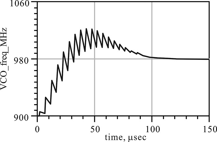
From Figure 11.35, Tlock is found to closely predict the lock time of the PLL. Many ripples appear because the loop bandwidth is not sufficiently narrow compared with the comparison frequency.
11.6 Summary
• A PLL is composed of a phase detector, loop filter, VCO, and reference oscillator. The phase detector provides the output voltage proportional to the phase difference of the VCO and reference oscillator, which is characterized by the phase detector constant Kd (Volt/rad). The VCO in the PLL can be characterized by the tuning sensitivity Kv (rad/sec/V).
• At the PLL’s steady state, the phase detector output voltage is constant and not time-varying. When the loop filter is above the second order, the phase detector output voltage is 0 at the steady state. This condition is used to find the VCO frequency at the steady state.
• Inside the loop bandwidth of the PLL, the phase noise of the VCO output follows that of the reference oscillator, while the phase noise of the VCO output as it is appears outside the loop bandwidth.
• Frequency dividers are used in a PLL to make the frequencies of the VCO and reference oscillator close; these frequencies are incident to the phase detector inputs. Frequency dividers are usually composed of a fixed divider and a programmable divider. Usually, the dual modulus counter is used as the fixed divider for consecutive dividing.
• Adding the accumulator to the divider composed of a dual modulus counter and a programmable divider, fractional dividing is possible and a fraction synthesizer can be constructed, which can reduce the in-band noise floor of the synthesizer.
• Phase detectors can be implemented using a DBM, Exclusive OR, and a phase-frequency detector (PFD). The phase detector characteristic of a PFD is linear and one-to-one for the phase difference 0–2p. When a charge pump circuit is added to the PFD, phase detector output becomes the current proportional to the phase difference, which makes for easy implementation of the loop filter that includes an ideal integrator.
• The loop filters can be designed using an open-loop gain. The second-order loop filter can be designed by setting ωn to be equal to a loop bandwidth and damping ratio ζ = 0.707. The open-loop gain of the third-order loop filter shows a phase peak. The third-order loop filter can be designed by setting the phase peak frequency to be equal to the loop bandwidth and setting the loop gain at this frequency to be equal to 1
• The fourth- and higher-order loop filters can provide spur attenuation. A higher-order loop filter can be designed by optimization.
• PLL simulation in ADS is possible and the process for simulating the phase noise and lock time of the PLL is presented.
References
1. F. M. Gardner, Phase-Locked Loop Techniques, 2nd ed. New York: John Wiley & Sons, Inc., 1980.
2. U. L. Rohde, Digital PLL Frequency Synthesizers: Theory and Design, Englewood Cliffs, NJ: Prentice-Hall, Inc., 1983.
3. D. Barberjee, PLL Performance, Simulation, and Design, 4th ed. Indianapolis, IN: Dog Ear Publishing, 2006.
Problems
11.1 (ADS Problem) From Example 11.1, take fn = 40 kHz and plot the output phase noise of the frequency synthesizer. Then, plot the phase noise using ADS.
11.2 Express the output phase noise, θo, of Figures 11.4(a) and 11.4(b) in terms of θi and θn.
11.3 Use Figure 11P.1 to solve the following problems:

(1) What is the phase noise at a 10-Hz offset frequency when a 10-MHz crystal oscillator is multiplied by 100? Compare this to the phase noise of 1-GHz DRO at a 10-Hz offset frequency.
(2) A 10-MHz crystal oscillator is used as the reference oscillator and it must phase lock at a 1-GHz DRVCO using a PLL. Obtain the optimum loop bandwidth BW. Then, plot the phase noise of the phase-locked DRVCO.
11.4 Use Figure 11P.2 to solve the following problems:
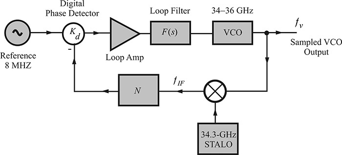
(1) From the figure, what is fv when N = 124?
(2) Calculate the output frequency fv when the frequency divider N is varied from 120–128.
11.5 Using Figure 11P.3, calculate the output frequency fo.

11.6 Using Figure 11P.4, solve the following problems:
(1) From the figure, what is fo?
(2) Calculate the output frequency when the frequency divider n varies from 160–660.
(3) Given the phase noise characteristics of the OCXO and VCXO that appear in Table 11P.1, determine the optimum bandwidth of the F2 loop filter.


11.7 Explain why the characteristics of the XOR phase detector are as shown in Figure 11.9.
11.8 Solve the following problems using Figure 11P.5:
(1) Given that the frequency of the VCO varies from 1.5 to 1.6 GHz when the tuning voltage is varied from 0 to 3 V, calculate the tuning sensitivity Kv in [rad/sec/V].
(2) Given that the PFD flows a current of 1.52 mA when the phase signal leads that of the reference signal, and conversely, that the PFD flows a current of -1.52 mA when the phase signal lags, as shown in Figure 11P.5, what is the phase detector constant Kd [A/rad]?
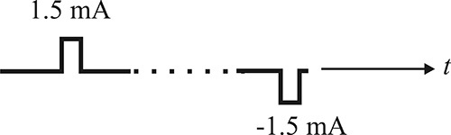
(3) For a reference oscillator with a frequency of 250 kHz, a PLL is built using the PFD in problem 11.8.2, above, the VCO with a frequency of 1.5 GHz from problem 11.8.1, above, and a frequency divider with a ratio N (N = 1500/0.25). Determine the open-loop gain of this PLL. Determine C2 and R2, shown in Figure 11P.6, to yield the bandwidth for the PLL of 10 kHz.
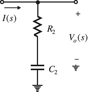
11.9 By referring to the spectrum analyzer’s manual and setting the SPAN to 0, explain the principles of measuring the time-varying power in an RBW.
11.10 For a given loop bandwidth ωc and a phase margin φ, calculate the exact values of the fourth-order loop filter using the appropriate software. Confirm the results using a Bode plot.
11.11 (ADS Problem) Given that the loop bandwidth is 10 kHz, the phase margin is 45°, the comparison frequency is 200 kHz, and fo = 900 MHz, after setting the phase detector constant for the tuning sensitivity of the VCO, as shown in Example 11.10, then calculate the element values of the second- and third-order loop filters and compare the loop gains.
11.12 (ADS Problem) In the simulation schematics shown in Figure 11.32, given that N0 = 4500, Fref = 200 kHz, and N_Step = 10, simulate the transient response after configuring the third-order loop filter with a loop bandwidth of 1 kHz.