
Chapter 10. Microwave Oscillators
Chapter Outline
10.4 Basic Oscillator Circuits
10.5 Oscillator Design Examples
10.7 Dielectric Resonator Oscillators (DRO)
10.1 Introduction
An oscillator is a circuit that generates a high-frequency sinusoidal waveform by converting DC energy delivered from a DC supply. Figure 10.1 shows the formation of an oscillation waveform in the oscillator, which can be divided into two phases: transient and equilibrium states. The amplitude of the sinusoidal waveform with a specific frequency component grows exponentially in the transient state. Then, after passing through the transient state, the waveform reaches the equilibrium state where the sinusoidal waveform with constant amplitude appears.
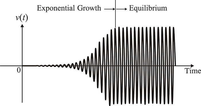
Thus, an oscillator design must determine whether or not the sinusoidal waveform with the desired frequency grows exponentially for a given circuit, as shown in Figure 10.1; it must then calculate the amplitude and frequency of the oscillation waveform at the equilibrium. For a given circuit, the condition necessary for a sinusoidal waveform with a specific frequency that will grow exponentially is called an oscillation start-up condition or simply oscillation condition. Since the signal level in an oscillation start-up is low, small-signal analysis can be used to examine the oscillation condition that tells whether or not the sinusoidal waveform with a specific frequency can grow exponentially. In contrast, since the signal level is not low enough at the equilibrium, large-signal analysis must be carried out. Therefore, the oscillation condition at equilibrium or simply the equilibrium condition should be described using large-signal parameters. Active devices such as transistors are generally nonlinear, and it is not possible to directly apply a linear circuit analysis concept, such as impedance or reflection coefficient, as a way to describe the oscillation at equilibrium. However, the level of harmonics in an oscillator circuit is generally low and large-signal impedance or gain can be defined by extending the concept of small-signal impedance or gain to describe the oscillation condition at equilibrium. This is explained in Appendix D.
In this chapter, we will discuss not only the oscillation start-up but also the equilibrium conditions. The large-signal impedance and reflection coefficient will be used to describe the equilibrium oscillation condition. Next, we will learn about the transformation of oscillator circuits and their design. The oscillation waveform is not an ideal sinusoidal waveform and its amplitude and phase vary randomly with time. The measurement technique and modeling of the randomly varying amplitude and phase will also be discussed in this chapter.
10.2 Oscillation Conditions
The small-signal oscillation (start-up condition) and large-signal equilibrium conditions of an oscillator circuit can be described in a number of ways. The reason for these various descriptions for the oscillation conditions is related to the ease of measuring the quantities that describe the oscillation conditions and it depends on the type of active devices that have evolved with advances in fabrication technologies. However, although the descriptions of the oscillation conditions may differ, they describe the same oscillation phenomena.
Earlier microwave oscillators were implemented using primarily one-port devices such as Gunn or IMPATT diodes. These oscillators can be decomposed into two parts, active device and load. The decomposed one-port network can easily be described using the impedance or reflection coefficient that can be measured directly. Thus, the one-port oscillation and equilibrium conditions that use the impedances or reflection coefficients are convenient for describing these one-port oscillators. As network analyzers are often used in microwave circuit measurements, the reflection coefficient is more direct and preferred for measurement than is the impedance. Thus, the one-port oscillation condition based on the reflection coefficient is a commonly used metric. The oscillation conditions in ADS are also based on the reflection coefficient. However, the impedance-based one-port oscillation conditions can still be applied to an oscillator circuit analysis after converting the reflection coefficient into the impedance.
Due to recent advances in microwave semiconductor technology, transistors such as the pHEMT or the HBT are primarily used in microwave applications instead of diodes such as the Gunn diode or the IMPATT diode. Thus, instead of the one-port oscillation condition, a technique based on an open-loop gain is more efficient. In other words, since the oscillator that uses transistors is, in general, implemented by a feedback network, the open-loop gain oscillation condition is obviously easy to apply. In this chapter, we will explain the open-loop gain conditions for the oscillator circuits that use transistors.
10.2.1 Oscillation Conditions Based on Impedance
10.2.1.1 Start-Up Conditions
In the oscillation condition analysis based on a one-port circuit, an oscillator can be viewed as a circuit composed of a one-port load and a one-port active part, as shown in Figure 10.2.
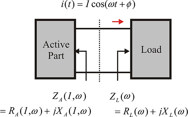
Figure 10.2 An oscillator circuit composed of a one-port load and the active part. The oscillator circuit is considered as the series connection of the one-port load and the active part.
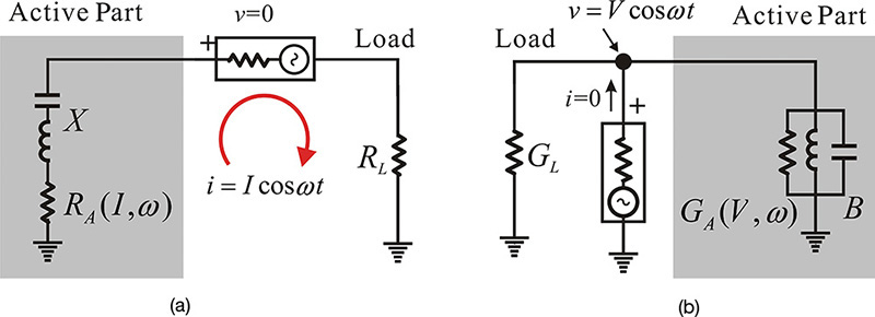
In the oscillator circuit, the active part represents the one-port network that includes an active device, such as the Gunn diode or an IMPATT diode, and has a negative resistance. In general, the impedance of the active device depends on the amplitude of the RF current I, as shown in Figure 10.2. Thus, ZA(I,ω) represents the large-signal impedance. The detailed explanation for obtaining the large-signal impedance, reflection coefficient, and gain using ADS or by measurement can be found in Appendix D. However, the load can be considered as a passive circuit that depends on frequency alone. The impedances of the active part and load can easily be measured using a network analyzer. Defining the impedance shown in Figure 10.2, the sum of the two impedances can be expressed as
Near the oscillation start-up point, the signal level is considered to be small, and since I ≅ 0, Equation (10.1) can be rewritten as Equation 10.2.
Let the frequency at which the imaginary part X (0, ω) = 0 be at ωo. Also, when R(0, ω) < 0 at ωo, the current I grows exponentially with time, which can be seen to satisfy the oscillation start-up condition. That is, in order to start the oscillation, the following conditions in Equations (10.3a) and (10.3b) must be satisfied, and their frequency-dependent variations are shown in Figure 10.3.
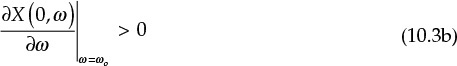
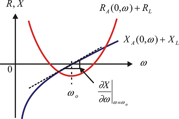
Figure 10.3 Series oscillation condition. The sum of the real part R < 0 and X = 0 at the oscillation frequency ωo. In addition, the slope of X with respect to frequency should be positive.
It must be noted that Equation (10.3b) can be interpreted as a series resonant condition and oscillation does not occur when the condition in that equation is not satisfied. This is the description of the oscillation condition in terms of impedance. A similar description can be obtained in terms of admittance. The load and active part in Figure 10.2 can be considered as a series connection. However, the connection can also be considered as a parallel connection, as shown in Figure 10.4. When viewed as a parallel connection, the voltage is common to both of the one-port circuits, whereas in the case of a series connection, the current is common.
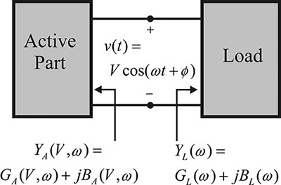
Figure 10.4 Oscillator circuit composed of a one-port load and the active part. The oscillator circuit is considered as the parallel connection of the one-port load and the active part.
The admittances of the active part and load are defined as follows:
YA(V, ω) = GA(V, ω) + jBA(V, ω)
YL(ω) = GL(ω) + jBL(ω)
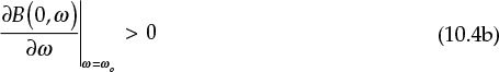
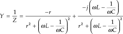
Denoting the sum of the admittances as Y = G + jB, then Equations (10.4a) and (10.4b),
express the similar start-up conditions that must be satisfied for the oscillation waveform to grow exponentially.
Note that the series oscillation condition in Equation (10.3) is the condition for the exponential growth of the RF current amplitude I, whereas the parallel oscillation condition in Equation (10.4) is the condition for the exponential growth of the RF voltage amplitude V when the active part and load are joined to form an oscillator. The series oscillation condition does not necessarily mean the exponential growth of V. Generally, the series oscillation condition described by the impedance does not satisfy the parallel oscillation condition described by admittance and vice versa. To investigate this, suppose that a fixed load (for example, Zo = 50-Ω load) is connected to the series resonating active part, as shown in Figure 10.5(a). Suppose that the sum of the active part and load impedances satisfies the series oscillation condition near the frequency ωo, X(ωo) = 0, -r + Zo < 0, and the slope is positive.
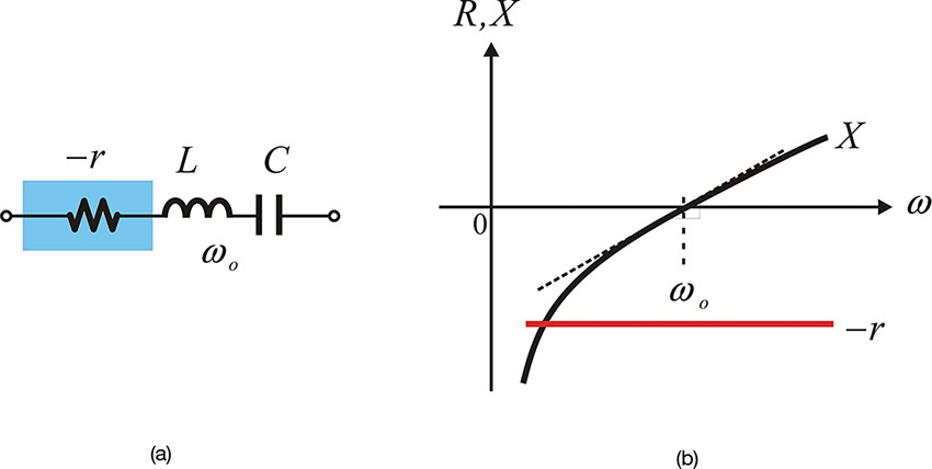
Figure 10.5 (a) Equivalent circuit of the active part and (b) the real and imaginary parts of the impedance for frequency
When the active part’s impedance is converted into admittance, the admittance of the active part becomes
The admittance Y can be drawn as shown in Figure 10.6.
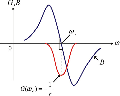
Figure 10.6 The admittance that corresponds to the impedance of Figure 10.5(b). Note that the slope of B with respect to frequency is negative at B = 0. Also, |G| < Yo, and parallel oscillation conditions are not satisfied as a result.
The sum of the real part of Y at ωo and the load conductance Yo becomes
That is, as the total conductance is positive and the result does not satisfy the parallel oscillation condition for which the RF voltage amplitude can grow exponentially. Thus, the series oscillation condition in Equation (10.3) does not provide the parallel oscillation condition given by Equation (10.4). Similarly, when the admittance that satisfies the parallel oscillation condition is converted into impedance, the converted impedance does not satisfy the series oscillation condition.
Note that the slope of B in Figure 10.6 can be seen to be negative. Thus, even when it shows positive conductance, if the slope of B at B = 0 is negative, it must be reinvestigated to determine whether or not the series oscillation condition is satisfied. Similarly, in terms of impedance, even though the total resistance R is positive, a point where X is 0 occurs, and if the slope of X is negative, it must be reinvestigated to determine whether or not the parallel oscillation condition is satisfied. Therefore, both oscillation conditions should be simultaneously investigated to check the oscillation condition. The reason for this is that the series oscillation condition describes the condition for the RF current amplitude I to grow exponentially, which is not the exponential growth condition of the RF voltage amplitude V.
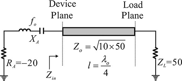
The active part of a series resonant oscillator connected to a load through a quarter-wavelength impedance inverter is shown in Figure 10E.1. To convert the load impedance of 50 Ω into 10 Ω, Zo of the impedance inverter is selected as Zo = (10 × 50)½ = 22.4 Ω. Discuss the oscillation condition at the load plane and the oscillation condition at the device plane in Figure 10E.1.
Solution
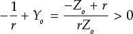
The load impedance seen from the active part is 10 Ω. A series resonant circuit is formed at the device plane and a series oscillation then occurs. Thus, the RF current amplitude with the resonance frequency will grow. Conversely, when the active part is seen from the load, the resistance at the resonance becomes Za = –(Zo)2/20 = –25 Ω, which is smaller than the load resistance. However, the impedance of the active part at the load side is given by Equation (10E.1).
The equation above means that the series connection is transformed into a parallel connection through the impedance inverter and a parallel resonance appears at the load side. Thus, since the real part of the active part is smaller than the load, it can be found to satisfy the parallel oscillation condition. Therefore, at the load side, a growth condition of the RF voltage is satisfied. In conclusion, by changing the reference plane, the series oscillation condition can be changed into the parallel oscillation condition.
The sum of the active part and load impedance R(0,ω) + jX(0,ω) is computed in Figure 10E.2. Explain where oscillations can occur and also discuss if further investigation is required to check the possibility of oscillation.
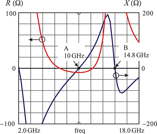
Figure 10E.2 Plot of the sum of the active part and load impedances. The series oscillation condition is satisfied at 10 GHz but the parallel oscillation condition may be satisfied at 14.8 GHz. The parallel oscillation condition should be checked again at 14.8 GHz.
Solution
From the figure, the possible point that satisfies the series oscillation condition described by the impedance is point A (10 GHz). However, oscillation is also possible at point B (14.8 GHz), which shows a parallel resonance. When the admittance satisfying the parallel oscillation condition is converted into an impedance, a positive resistance and negative slope appear at the parallel resonant frequency. Since the oscillation condition is investigated using the sum of the impedance alone, the possibility of satisfying the parallel oscillation condition at point B is not certain. Therefore, it is necessary to plot the sum of the admittance at 14.8 GHz (point B) to check the occurrence of a parallel oscillation.
10.2.1.2 Equilibrium Conditions
In Figure 10.2, when the equilibrium is reached, the amplitude of i(t), Io, becomes constant. Applying the KVL, we obtain Equation (10.5),
and since Io ≠ 0,
Rewriting Equation (10.6),
Thus, Equations (10.7a) and (10.7b) must be satisfied at equilibrium.
The ωo given by the oscillation start-up condition does not generally satisfy XA(Io,ω) + XL(ω) = 0. Thus, the oscillation frequency at equilibrium can be slightly different from the frequency determined by the oscillation start-up condition. In general, for a high Q circuit, the oscillation frequency primarily appears near the frequency determined by the oscillation start-up condition. Assuming that XA(I, ωo) does not vary with I, the RF current amplitude Io at equilibrium can be found by plotting the sum resistance R with respect to the RF current amplitude I. Figure 10.7 shows a plot of R(I,ω) for I. In Figure 10.7, the value of R at the small-signal I ≅ 0 is found to be negative. The RF current amplitude will increase exponentially, thereby increasing along the x-axis. Conversely, when I is larger than Io at the equilibrium point, since the value of R will be positive, the RF current amplitude decreases exponentially, thereby decreasing along the –x direction. As a result, equilibrium is attained at the point where the value of R is 0, that is, the point where the RF current amplitude is Io and thus a steady-state current amplitude appears.
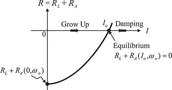
Figure 10.7 Plot of the series sum resistance with respect to the current amplitude I. For small I, I will grow exponentially because R < 0. In contrast, I will decrease because R > 0 for I > Io. Eventually the equilibrium is formed at Io.
In addition, the real and imaginary parts of the large-signal admittance at equilibrium condition, like the impedance equilibrium condition, are expressed in Equations (10.8a) and (10.8b), respectively.
Similarly, the oscillation frequency at the equilibrium given by Equation (10.8b) is slightly different from the oscillation frequency determined by the oscillation start-up condition. When BA(V,ωo) is assumed to be constant for the change of V, the equilibrium can be seen to be attained at an RF voltage amplitude Vo using reasoning similar to that for the impedance equilibrium condition.
10.2.1.3 Oscillation Start-Up and Equilibrium Condition Analysis Using ADS
Since it is necessary to calculate the sum of the series impedance in order to simulate a small-signal start-up oscillation condition using ADS, a port is inserted in series between the load and the active part, as shown in Figure 10.8(a). After the one-port S-parameter analysis, the impedance of ZA + ZL at the small-signal start-up oscillation can be obtained. However, the admittance YA + YL is obtained by inserting a port in parallel between the load and the active part, as shown in Figure 10.8(b), and then performing S-parameter analysis. Thus, to investigate the possibility of oscillation using the admittance or impedance obtained through S-parameter analysis, two S-parameter analyses should be simultaneously performed, as shown in Figure 10.8.
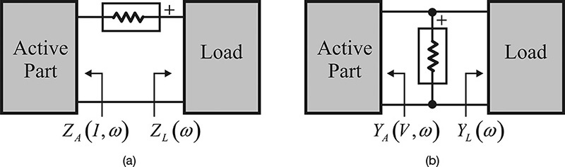
Figure 10.8 Simulation setup for checking the small-signal oscillation condition: (a) series and (b) parallel
Next, the large-signal equilibrium condition must be calculated in ADS to determine the exact oscillation frequency and amplitude. This is accomplished by connecting a large-signal port, as shown in Figure 10.9, and performing a harmonic balance simulation. For series oscillation, the circuit is connected, as shown in Figure 10.9(a), to determine the equilibrium oscillation point. For parallel oscillation, as shown in Figure 10.9(b), the circuit is connected to determine the equilibrium oscillation point.
From Figure 10.9(a), since the sum of the impedances at the series oscillation equilibrium point is 0, the voltage across the port becomes 0. In that case, the amplitude of the current flowing through the port will only be the RF current amplitude at equilibrium. In contrast, since the sum of the admittance becomes zero at the parallel-oscillation equilibrium point, the current flowing out from the port becomes 0 and thus the RF voltage amplitude across the port will be the amplitude of the voltage at equilibrium.
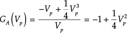
For the active device represented by the current–voltage relationship as
plot the conductance GA of the active device; then, by simulation, plot the total conductance G = GA + GL when GL = 0.2. In addition, obtain the voltage when the total conductance is 0 and verify that the voltage is the oscillation output voltage at equilibrium.
Solution
When a sinusoidal voltage is applied to the active device, the current is
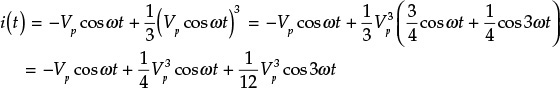
Thus, the large-signal conductance becomes
To confirm this by simulation, the given active device can be configured using an SDD (symbolically defined device), as shown in Figure 10E.3. In that figure, the parallel resonant circuit resonating at 1 GHz is connected in parallel with the SDD in order to set the oscillation frequency to 1 GHz. Since the parallel resonant circuit can cause problems at the DC operating point, a DC block is inserted in the parallel resonant circuit. After these settings and the simulation, the following equation in Measurement Expression 10E.1 is entered in the display window to plot the total conductance G, the result of which is shown in Figure 10E.4.
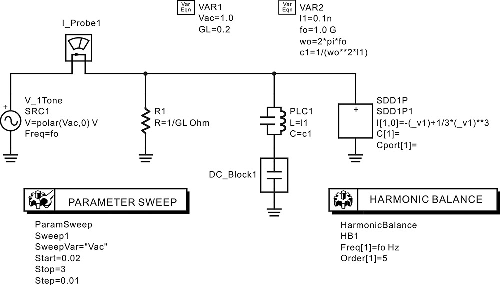
Figure 10E.3 Computation of the large-signal impedance for Vac. DC_Block1 is inserted so as not to disturb the DC bias.
![]() G=real(I_Probe.i[::,1])/Vac
G=real(I_Probe.i[::,1])/Vac
Measurement Expression 10E.1 Conductance G calculation
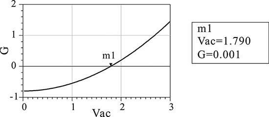
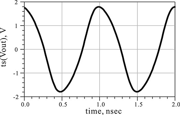
In Figure 10E.4, G is the same as the theoretically calculated conductance, which is found to be a parabola. In addition, the value of Vac where G is 0 can be seen to be approximately 1.8 V. Thus at the oscillation equilibrium, the RF voltage amplitude of 1.8 V will appear. To confirm this, OscPort, which will be explained in the next section, can be used to verify the value of Vac. The oscillation output voltage can be obtained by setting up the schematic shown in Figure 10E.5 and simulating it. The simulated waveform is shown in Figure 10E.6. The waveform in that figure shows a significant amount of distortion due to harmonics, but the amplitude of the oscillation waveform can be seen to be approximately 1.8 V.
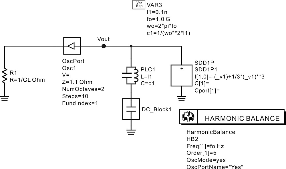
Figure 10E.5 Simulation schematic for the oscillation waveform. OscPort in the Harmonic Balance simulator is used to obtain the large-signal oscillation waveform of the oscillator circuit.
10.2.2 Oscillation Conditions Based on the Reflection Coefficient
10.2.2.1 Start-Up and Equilibrium Conditions Based on the Reflection Coefficient
The oscillation condition based on the reflection coefficient is widely used because it is easier to measure the reflection coefficient at high frequencies compared to the measurement of impedance. The oscillation condition based on the reflection coefficient is similar to the oscillation condition based on impedance discussed earlier. In Figure 10.10, the reflection coefficients of the active part and load are defined for the same reference impedance Zo, and their one-port reflection coefficients are ΓA and ΓL, respectively.
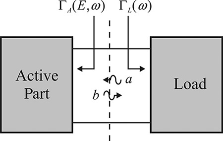
Figure 10.10 Oscillator circuit based on the reflection coefficient. ΓA and ΓL are the reflection coefficients defined with the same reference impedance. In the case of ΓA, it is also a function of |a| = E.
When the incident voltage a = E⋅cosωt corresponding to the available power of PA = ½E2 is applied from the load, the new reflected voltage from the load a’ after a round-trip between the active part and the load is expressed in Equation (10.9).
The reflected voltage a’ becomes a new incident voltage that again makes a round-trip between the active part and the load. Thus, for exponential growth, the following start-up conditions must be satisfied, as expressed in Equations (10.10a) and (10.10b).
Here, ΓA(0,ωo) represents the small-signal reflection coefficients of the active part. Equation (10.10a) is the condition that must be satisfied for the signal to grow through the repetition of round-trips, while Equation (10.10b) is the condition requiring that the phase remain unchanged when these round-trips repeat.
In addition, for the oscillation conditions given by Equations (10.10) to be stable, the slope of Equation (10.10b) for the frequency must be negative. This is expressed in Equation (10.11).
The example of the oscillation condition that satisfies Equations (10.10) and (10.11) is shown in Figure 10.11. The magnitude and phase of ΓAΓL that satisfy the oscillation condition are plotted in that figure, where it can be seen why the condition in Equation (10.11) is necessary. When the frequency is lower than the oscillation frequency, a positive phase occurs, and by repeated round-trips, the frequency increases as the phase continues to increase until it eventually approaches the oscillation frequency. In contrast, when the frequency is higher than the oscillation frequency, the phase becomes negative and, by repeated round-trips, the phase decreases continuously and eventually attains equilibrium at the frequency of oscillation. Thus, Equation (10.11) provides a stable oscillation.
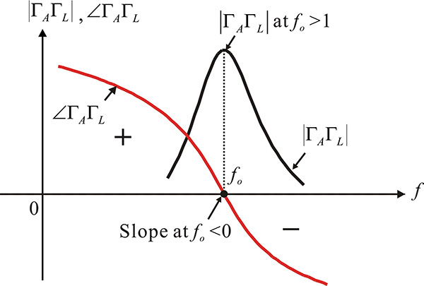
Figure 10.11 Plot of small-signal ΓLΓA, which can be represented by ΓLΓA (0,w). For oscillation at fo,|ΓLΓA (0,w)| > 1 and ∠ΓLΓA (0,w) = 0 at fo should be satisfied. Also, the slope of ∠ΓLΓA (0,w) with respect to frequency should be negative for stable oscillation.
It must be noted that the oscillation conditions given by Equation (10.10) obviously guarantee oscillation. However, oscillation can also occur under other conditions and thus the conditions given by Equation (10.10) are the conditions sufficient for oscillation. Furthermore, the conditions change when the reference impedance, used to measure the reflection coefficients of the active part and load, changes. This is summarized in Appendix F.
The plot of ΓLΓA(E,ωo) for E is shown in Figure 10.12. Similar to the impedance oscillation conditions described earlier, E will grow exponentially at the small-signal because |ΓLΓA(E,ωo)| > 1 and increases along the x-axis, while E decreases when E becomes greater than Eo. Therefore, the equilibrium is achieved at Eo. That equilibrium is expressed in Equations (10.12a) and (10.12b).

Figure 10.12 Plot of ΓAΓL with respect to the available power. For small E, E will grow through repeated round-trip because |ΓLΓA (0,w)| > 1. In contrast, E will decrease because |ΓLΓA (0,w)| < 1 for E > Eo. Eventually the equilibrium is formed at Eo.
In other words, at the equilibrium point, the magnitude of the product of the reflection coefficients due to continuous round-trips is 1 and its phase is 0°.
10.2.2.2 Circuit Implementation
The previously described oscillation condition based on the reflection coefficient can be implemented using a circulator, as shown in Figure 10.13.
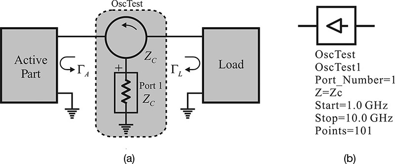
Figure 10.13 a) Measurement of ΓAΓL. The reflection coefficient seen from the port becomes ΓAΓL. (b) OscTest in ADS. Z represents the port impedance.
As shown in Figure 10.13(a), when the load and active part are connected to a broadband circulator with the reference impedance ZC, the reflection coefficient S11 at the port can be expressed as S11 = ΓAΓL. Note that the computed ΓAΓL depends on the reference impedance ZC of the port. The different port impedance will result in a different value for ΓAΓL. The oscillation condition based on the reflection coefficient is thus a function of the reference impedance ZC. The circulator and port in the shaded box shown in Figure 10.13(a) are already implemented as OscTest in ADS, as shown in Figure 10.13(b). The variable Z of OscTest represents ZC in Figure 10.13(a). The OscTest computes ΓAΓL for the frequency range that is specified as Start and Stop.
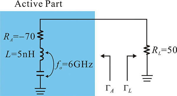
This Example considers a small-signal series oscillation circuit shown in Figure 10E.7. For the reference impedance of 100 Ω, calculate ΓAΓL and verify that this is the same as computed using OscTest whose Z is set to 100 Ω.
Solution
The magnitude and phase of S11 is computed using OscTest with Z = 100 Ω as shown in Figure 10E.8.
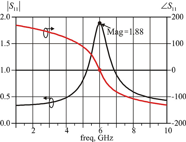
In that figure, |S11| at fo = 6 GHz is greater than 1, and the phase is 0°. In addition, the phase slope with respect to frequency can be seen to be negative. Thus, the oscillation conditions based on the reflection coefficient are satisfied.
On the other hand, calculating ΓAΓL at the oscillation frequency of 6 GHz,
which is the same as the value of mag(S11) shown in Figure 10E.8.
Notably, ΓAΓL = 0 when ZC is set at 50 Ω instead of 100 Ω, and the oscillation conditions in Equation (10.12) are not satisfied. However, this is the oscillation condition variation due to the change of ZC. The oscillator circuit in this example clearly oscillates although ΓAΓL = 0. Therefore, selecting the appropriate reference impedance makes it easy to check the oscillation condition. For more information, refer to Appendix F.
10.2.2.3 Equilibrium Based on the Reflection Coefficient
The oscillation start-up condition based on the reflection coefficient can be used to derive the large-signal equilibrium conditions. That is, irrespective of a parallel or series oscillation, the product of the reflection coefficients ΓAΓL must be 1 at equilibrium. Figure 10.14 shows the circuit measuring ΓAΓL, where the port is replaced by the large-signal port.
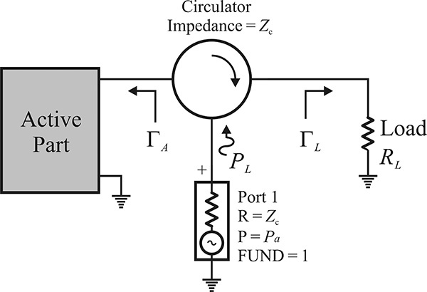
Figure 10.14 Computing method for a large-signal equilibrium in an oscillator. For a small signal, the oscillator circuit generates power and the port consumes the oscillation power; however, the port delivers the power to the oscillator circuit at a large-signal level. Thus, the equilibrium is formed when the dissipation power of the port is 0.
Denoting the available power from the port as Pa, the power delivered to the oscillator circuit from the port is Pa(1 – |ΓLΓA|2). Thus, when Pa is small, the delivered power becomes negative because |ΓLΓA| > 1. As a result, the port consumes the power rather than delivering it to the oscillator circuit. At equilibrium, the port is found to deliver no power to the oscillator circuit because |ΓLΓA| = 1. Therefore, the equilibrium point can be found by determining when the delivered power from the port PL becomes 0. Then, every voltage and current in the oscillator circuit at equilibrium can be obtained by calculating the currents and voltages of the oscillator circuit at the port power where delivered power from the port becomes 0.
Thus, to determine the large-signal equilibrium state using the reflection coefficient, the available power and frequency of the port is altered to yield |ΓAΓL| = 1. Then, using the determined port power and the frequency at equilibrium, every current and voltage inside the oscillator circuit can be calculated; in turn, this calculation can be used to determine the waveforms of every node in the oscillator circuit at equilibrium. These operations can be performed automatically in ADS, and this is usually done using the OscPort. That is, by performing the simulation using the OscPort in conjunction with the Harmonic Balance simulator (i.e., a simulation in which the large-signal available power of the port is varied to determine the oscillation power and frequency at equilibrium), the oscillation at equilibrium can be found. The OscPort is shown in Figure 10.15(b). Figure 10.15(a) shows the concept of OscPort in ADS. The oscillation at equilibrium can be obtained by using the HB simulator together with the OscPort shown in Figure 10.15(b).
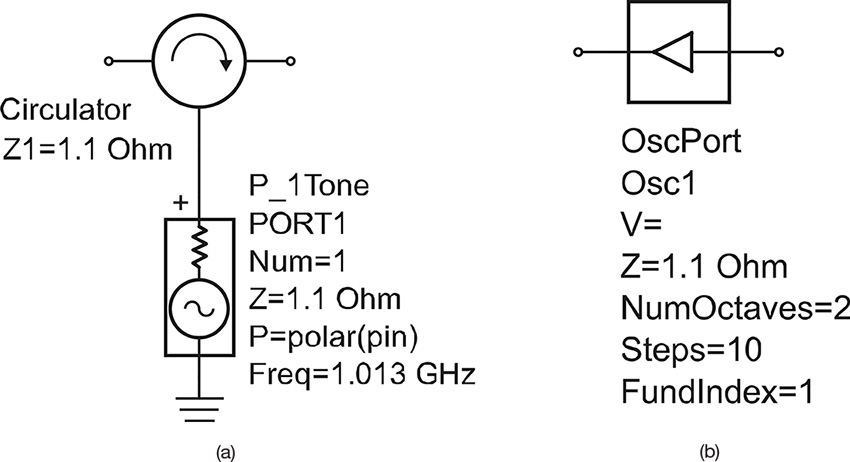
The Z of the OscPort in Figure 10.15(b) is the reference impedance of the circulator. FundIndex is the index of the estimated oscillation frequency in the HB simulator. It represents the simulation for the fundamental frequency, which in most cases is 1. Since the oscillation frequency at equilibrium differs from the estimated small-signal oscillation frequency, NumOctaves is specified to determine the frequency tuning range. When NumOctaves = 2, the oscillation frequency is sought for the frequency range that varies from 0.5 to 2 times the estimated frequency.
The diode admittance is denoted as YA = –G(A) + jB(A). Here, A represents the amplitude of the fundamental voltage. One diode has G(A) = g(0) – k1A and the other has G(A) = g(0) – k2A2, as shown in Figures 10E.9(a) and (b), respectively.
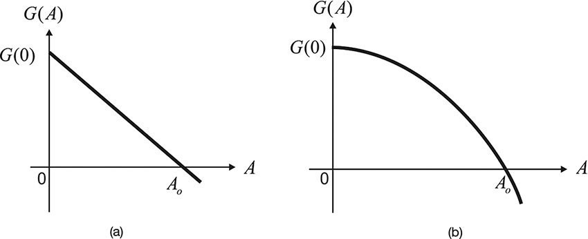
Figure 10E.9 G(A) with respect to voltage amplitude A: (a) linear decrease and (b) quadratic decrease
The load values giving maximum oscillation output power are known to be 1/3⋅G(0) and 1/2⋅G(0), for G(A) in Figures 10E.9(a) and (b), respectively. In Example 10.4, – G(A) = 1 – 1/4⋅A2. Thus, G(A) delivers the maximum oscillation output power to the load when the load conductance GL is equal to 0.5. Confirm this through simulation and calculate the maximum oscillation output power.
Solution
As mentioned earlier, the maximum oscillation power occurs at GL = 0.5 and since the amplitude at equilibrium must satisfy
it can be seen that A = (2)½. Thus, the maximum output power is
To confirm the oscillation output power for the change of GL, the harmonic balance simulation is performed using OscPort, as shown in Figure 10E.10. After simulation, the equation shown in Measurement Expression 10E.2 is entered in the display window to calculate the output power PL delivered to the load GL.
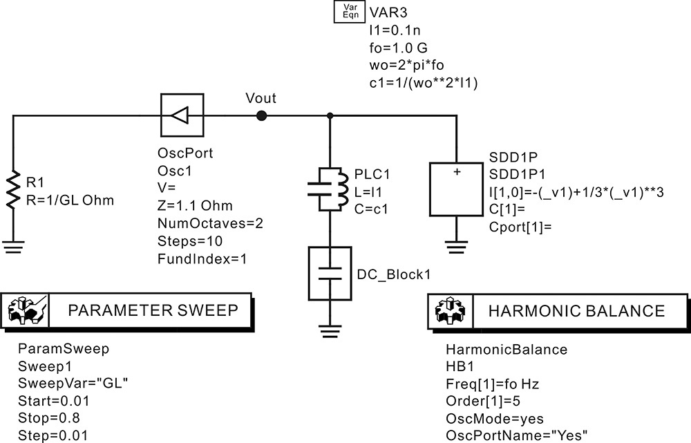
![]() PL=1/2*GL*mag(Vout[::,1])**2
PL=1/2*GL*mag(Vout[::,1])**2
Measurement Expression 10E.2 Equation for the delivered power to the load
The delivered power PL is shown in Figure 10E.11. As expected, the maximum output power is 0.5 W at GL = 0.5.
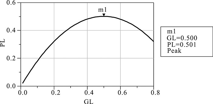
Figure 10E.11 Oscillation output power for the GL change. As expected, the maximum oscillation power 0.5 W is achieved at GL = 0.5.
10.2.3 Start-Up and Equilibrium Conditions Based on Open-Loop Gain
The one-port oscillation condition described earlier that uses the impedance or reflection coefficient is a direct method for analyzing oscillator circuits employing diodes, but not for analyzing oscillator circuits using transistors, which can be configured as oscillators using a feedback network. In the case of oscillators that use the feedback network, the description based on the one-port oscillation conditions generally makes it difficult to understand the role of the feedback network. Instead of the reflection coefficient or the impedance used in one-port oscillation conditions, the use of an open-loop gain makes it easy to understand oscillators that employ feedback. The open-loop gain also facilitates an understanding of the maximum output power condition and phase noise of oscillators using feedback. The open-loop gain is easily obtained when the reverse gain of a transistor is small, which enables the calculation of the open-loop gain in the direction of power delivery. However, at high frequency, the reverse gain is not small and it is not easy to calculate the open-loop gain due to the bidirectional properties of transistors. Recently published papers have revisited the calculation of the open-loop gain, taking the bidirectional properties into consideration.1, 2 Thus, the open-loop gain method will be widely used in the design of oscillators employing feedback.
1. M. Randall and T. Hock, “General Oscillator Characterization Using Linear Open-Loop S-Parameters,” IEEE Transactions on Microwave Theory and Techniques 49, no. 6 (June 2001): 1094–110.
2. R. Rhea and B. Clausen, “Recent Trends in Oscillator Design,” Microwave Journal, January 28, 2004.
10.2.3.1 Start-Up and Equilibrium Conditions Based on Open-Loop Gain
Figure 10.16 shows an oscillator configuration in which the output of the amplifier is fed back through a resonator. Here, the feedback loop is broken, which is done to obtain the open-loop gain.

Figure 10.16 Oscillator configuration with feedback network. To measure the open-loop gain, the feedback loop is broken. The test signal is applied to one port where the loop is broken and the open-loop gain is obtained by measuring the output appearing at the other port.
In the figure, the gain G(A,ω) of the amplifier can be considered to vary with the input signal amplitude A, and the transfer function of the resonator can generally be expressed as shown in Equation (10.13),
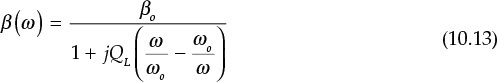
where βo is the transmission coefficient at the resonant frequency wo, and QL represents the loaded Q of the resonator. The open-loop gain L(A, w) is defined as Equation (10.14),
which is the output voltage per loop trip of the input signal. When a sinusoidal signal of A·cos(ωot) is applied to the input of Figure 10.16, a signal of L(A,ωo)⋅Acos(ωot) appears at the loop output. It must be noted that the output signal has the same phase as the input signal and only the amplitude varies. The output signal L(A,ωo)⋅Acos(ωot) is repeatedly applied to the input of Figure 10.16 when the loop is closed. If the loop gain |L(A,ωo)| > 1, the amplitude grows after every trip of the loop. Therefore, in order for the signal to grow as a small signal, |L(A,ωo)| > 1 at the frequency ωo with the phase 0°. Then, oscillation can be formed. This is called the Barkenhausen Criterion and can be expressed as shown in Equations (10.15a)–(10.15c).
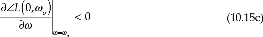
When the conditions above are satisfied, the amplitude grows by repeated feedback and oscillation can occur. The reason Equation (10.15c) must be satisfied is that when the frequency is lower than the resonant frequency, the phase of the open loop gain in Figure 10.17 becomes positive, and thus the phase grows positively for every trip of the loop. The continuous increase in the phase represents an increase in frequency, eventually approaching the resonant frequency. In contrast, when the frequency is higher than the resonant frequency, the phase of the open loop gain in Figure 10.17 becomes negative and decreases negatively for every trip of the loop, and the continuous decrease in phase represents a decrease in frequency, and thus approaches the resonant frequency. On the other hand, when the phase response of the open-loop gain is opposite of that given by Equation (10.15c), even when there is a small phase jitter, it will be away from the resonance frequency, and oscillation will not occur. Thus, Equation (10.15c) is an important criterion in determining the occurrence of oscillation.
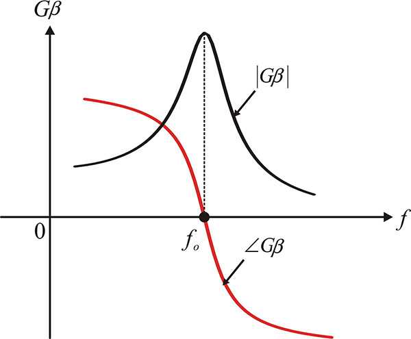
The typical small-signal open-loop gain L(0,ω) is shown in Figure 10.17. The frequency response characteristics shown in Figure 10.17 satisfy the conditions of Equation (10.15). Because the gain G(0,ω) is almost constant, the shape of the open-loop gain with frequency generally resembles the frequency response of the resonator given by Equation (10.13). The maximum value of the open-loop gain occurs at the resonant frequency ωo and decreases below and above the resonant frequency, as shown in Figure 10.17. Furthermore, the phase is 0° at the resonant frequency; the phase approaches 90° below the resonant frequency, while it approaches –90° above the resonance frequency.
The change of the open-loop gain according to the amplitude is plotted in Figure 10.18. For small signals (A ≅ 0), as the magnitude of the open-loop gain is greater than 1, the amplitude A increases exponentially. The open-loop gain is reduced due to the increase in A. In contrast, when the amplitude is greater than the equilibrium point, the amplitude decreases because the open-loop gain is less than 1. Eventually, the amplitude A reaches Ao at the point where the open loop gain is 1. Therefore, the oscillation frequency is determined by Equation (10.16)
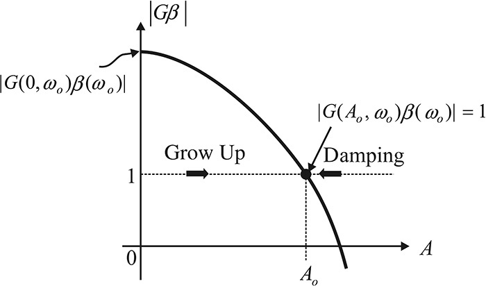
Figure 10.18 The open-loop gain for amplitude A. For small A, A will grow through repeated round-trips because |Gβ| > 1. In contrast, A will decrease because |Gβ| < 1 for A > Ao. Eventually, the equilibrium is formed at Ao.
and the oscillation amplitude Ao is determined by Equation (10.17).
10.2.3.2 Open-Loop Gain
Compared to the one-port method, the open-loop gain method is obviously more intuitive and easier to apply when investigating the oscillation condition for an oscillator circuit using a feedback network. The oscillator circuit using feedback can be represented conceptually, as shown in Figure 10.19(a). In order to calculate the open-loop gain of the oscillator circuit, that circuit is cut to break the feedback, as shown in Figure 10.19(b).
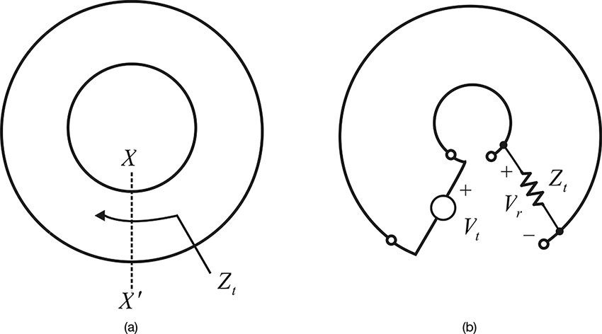
Figure 10.19 (a) Conceptual feedback network and (b) the open-loop network for calculating open-loop gain. The open-loop gain is equal to Vr/Vt.
The open-loop gain can be computed by applying a test source Vt and measuring the return voltage Vr at the load with the impedance Zt, which is equal to that looking into the source side prior to breaking the loop. However, it is generally difficult to find the impedance Zt at the cut plane. To this end, the feedback is considered as an infinite number of identical open-loop networks connected end to end. When the two-port S-parameters for the two-port open-loop network in Figure 10.19(b) are defined as Sij, the open-loop gain L can be expressed as Equation (10.18).

For L(ω) to satisfy the oscillation conditions in Equation (10.15), the open-loop network can oscillate when it is closed. In that equation, S11, S22, and S12 are generally small, and L(ω) is simplified as
From Equation (10.19), the oscillation condition is determined as
The feedback-type oscillator can easily be designed using Equations (10.20a) and (10.20b). The feedback-type oscillator is usually composed of cascaded two-port circuits. For example, the oscillator circuit in Figure 10.16 can be viewed as the cascaded connection of an amplifier and a resonator. Using the S-parameters of each block, the two-port S-parameters of the open-loop network can be obtained. Also, if each block is matched, the open-loop gain is simply the product of each block’s S21, and the oscillation frequency satisfying Equations (10.20) can be easily found. Once the open-loop gain satisfying Equation (10.20) at the oscillation frequency is obtained, the oscillator can be built up simply by closing the open loop. In addition, the large-signal equilibrium conditions can be obtained from the response of the open-loop gain for amplitude change, which can be computed using OSCPort in ADS.
The circuit shown in Figure 10E.12 is a Colpitts oscillator. Calculate its oscillation frequency by the open-loop gain method using ADS.
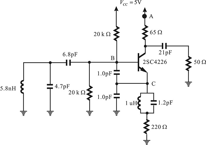
In the circuit shown in Figure 10E.12, the ground point is eliminated and a new ground point C is set at the transistor’s emitter. With the changed ground point, the input of the open loop is defined by the base emitter (B–C plane) of the transistor and the open loop is formed by breaking the oscillator circuit at the B–C plane, as shown in Figure 10E.13. The collector-emitter voltage and base current are determined in advance through DC simulation for the circuit in Figure 10E.12. In order to maintain the DC operating point of the transistor, the determined collector-emitter voltage and base current are supplied by a new DC current source and a voltage source, as shown in Figure 10E.13. After setting up the circuit, the S-parameter simulation is carried out.
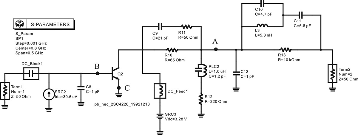
Figure 10E.13 Circuit for calculating the open-loop gain. First, DC analysis is carried out for the circuit shown here. Then, the computed base current and VCE are applied to bias 2SC4226, as shown in this figure. Finally, the circuit, which is cut along points B and C, is redrawn and the new ground point is set to point C.
After simulation, the equation in Measurement Expression 10E.3 is entered in the display window to compute and plot the open-loop gain.
![]() G=(S(2,1)-S(1,2))/(1-S(1,1)*S(2,2)+S(1,2)*S(2,1)-2*S(1,2))
G=(S(2,1)-S(1,2))/(1-S(1,1)*S(2,2)+S(1,2)*S(2,1)-2*S(1,2))
Measurement Expression 10E.3 Open loop gain calculation using the simulated S-parameters
The magnitude and phase of the open-loop gain are shown in Figure 10E.14. The oscillation frequency is approximately 827 MHz. To compute the large-signal oscillation frequency, the previously described OscPort is inserted in the oscillator circuit in Figure 10E.12. The calculated oscillation frequency confirms the obtained 827 MHz shown in Figure 10E.14. Note that the ground point was moved to the transistor’s emitter for calculating the open-loop gain, which made the calculation easy. This change to the ground point is frequently used in oscillator design and is called virtual ground technique.
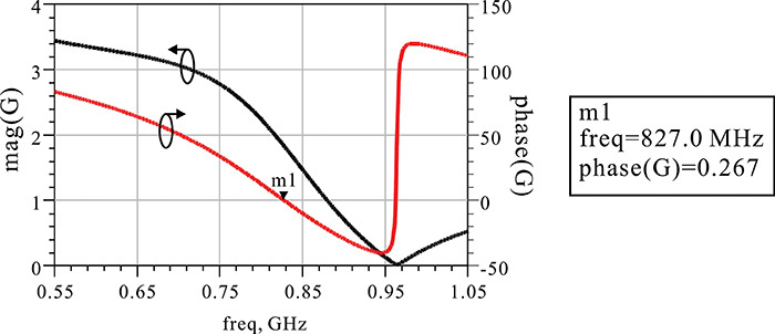
Figure 10E.14 Calculated open-loop gain. The phase of the open-loop gain crosses 0 at 827 MHz, at which the open-loop gain G > 1. Thus, the small-signal oscillation condition based on the open-loop gain is satisfied at 827 MHz.
10.3 Phase Noise
10.3.1 Spectrum of an Oscillation Waveform
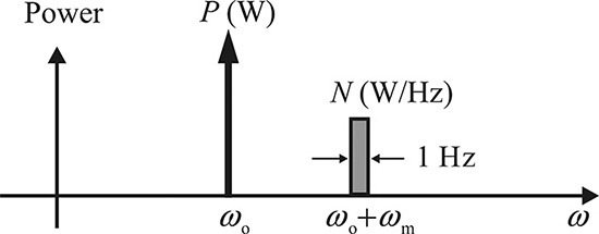
The output waveform of an oscillator is not a pure sine wave and its amplitude and phase fluctuate with time. Thus, denoting the oscillation output power across a 1-Ω resistor as P, the waveform can be expressed in time domain as shown in Equation (10.21).
Here, we assumed the power P across the 1-Ω resistor but it does not lose generality. The a(t) represents the fluctuation of the amplitude, and ϕ(t) represents the fluctuation of the phase in the time domain. The a(t) is called the amplitude modulation (AM) noise while ϕ(t) is called the phase noise of the oscillator.
Two major issues are associated with understanding amplitude and phase noises. The first is the mathematical model or mechanism of the amplitude and phase noises and the second is how to measure these noises. We will first discuss the measurement method and then the mathematical model of the phase noise will be explained.
When the waveform represented by Equation (10.21) is observed on a spectrum analyzer, the spectrum is usually similar to that shown in Figure 10.20. The spectrum analyzer can be thought of simply as equipment showing the spectral power of an input signal that is the output power of a narrow-band filter. The center frequency of the narrow-band filter moves with time while maintaining the user-specified resolution bandwidth (RBW). Thus, the spectrum analyzer shows the power within the RBW on the axis of the frequency. In displaying the power with the RBW, the spectrum analyzer averages the measured power within the RBW in a given amount of time. The VBW (video bandwidth) is used as a measure of time averages. Usually, because VBW is expressed as a frequency, it is the reciprocal of the average time and so it is smaller than the RBW. The spectrum shown in Figure 10.20 is measured for a span of 1 MHz at the center frequency of 35.349 GHz. Also, RBW = 10 kHz and VBW = 3 kHz. Thus, the spectrum in Figure 10.20 represents average power in the 10-kHz bandwidth over 1/3 msec.
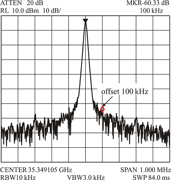
Furthermore, when Equation (10.21) is expanded, it can be considered as the superposition of the sinusoidal component of frequency ωo, whose power is P and a noise power. The sine wave power appears as the power of the center frequency component and the noise power has a distribution that is spread around the center frequency. Since the spectrum of the sinusoidal wave of frequency fo has the spectrum of Pδ(f – fo), a power P appears when fo is within the RBW, otherwise P = 0. In addition, the value of the sinusoidal power P does not change even when the RBW is changed; that is, whether the RBW is lowered or increased, the same power appears. However, it should be noted that noise density (noise power per bandwidth) is constant in the case of the noise. Thus, by lowering the RBW, the noise power measured within the RBW is lowered, whereas the noise power measured within the RBW is raised when the RBW increases.
In Figure 10.20, the ratio of the center frequency power (or the carrier power) to the noise power at a frequency offset of 100 kHz from the center frequency is measured to be about –60.33 dBc. Calculate the carrier to noise power ratio measured at a 100-kHz offset when the RBW is changed to 1 Hz. Also calculate the power when the RBW is changed to 1 kHz.
Solution
As the power of the center frequency is the sine wave power, it does not change even if the RBW is changed. However, the power at the 100-kHz offset is a noise power and thus changes when the RBW is changed. Since the power is –60.33 dB when the RBW = 10 kHz, then –60.33 dB/10 kHz = –100.33 dB/Hz. In addition, when the RBW is changed to 1 kHz, the power at the marker can be measured by the same method to be –70.33 dB.
The spectrum in Figure 10.20 represents the contribution of a sine wave’s output and noise. The noise power also comes from the combined effect of fluctuations in the amplitude and phase. However, for most oscillators, because the fluctuation effect coming from the amplitude is low compared to that coming from the phase, the spectrum noted above is generally known to occur due to phase fluctuation.
The following conceptual experiment can be thought of as the proof for the claim above of the phase noise dominance in the measured spectrum. That is, in order to eliminate the AM noise due to the amplitude fluctuation, the oscillator output is passed through a limiter and then the output is passed through a narrow bandwidth bandpass filter to remove harmonics. The resulting spectrum reflects only the phase fluctuation. However, in most cases, almost the same spectrum is obtained as a result of this experiment, which leads to the conclusion that the spectrum in Figure 10.20 is mostly due to the phase noise. In addition, because the AM noise can always be removed using the limiter and filter, the spectrum noted above is considered to represent the phase noise.
10.3.2 Relationship between Phase Noise Spectrum and Phase Jitter
To see the relationship between the spectrum shown in Figure 10.20 and the phase fluctuation, consider a part of the noise spectrum at a frequency offset of ωm from the center frequency and the sine wave output shown in Figure 10.21. The waveforms in the time domain can be expressed as
Expanding Equation (10.22) using the additive theorem of trigonometric functions and assuming that P >> N, v(t) can be written as
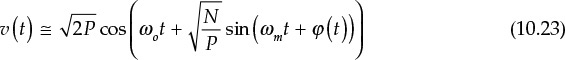
Thus, the carrier is found to be phase-modulated by the noise signal and its power is almost equal to the carrier power. Since the maximum phase deviation is (N/P)½, then the peak phase jitter becomes (N/P)½. Alternatively, the phase jitter can be determined using a phasor diagram. The carrier becomes the phasor that rotates counter-clockwise and the noise phasor is placed at the end of the carrier phasor, which becomes a rotating phasor with angular velocity ωm, as shown in Figure 10.22. Therefore, the maximum phase error for P >> N is obtained with Equation (10.24).
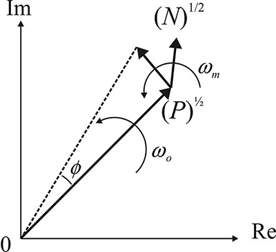
Figure 10.22 Phasor diagram of Equation (10.22). The carrier can be represented by the phasor that rotates counterclockwise with an angular velocity of ωo, while the noise signal in Equation (10.22) can be represented by the phasor at the end of the carrier phasor rotating counterclockwise with an angular velocity of ωm.
Thus, the phase fluctuation is a function of the offset frequency and the maximum phase jitter at the offset frequency of ωm is expressed in Equation (10.25).
Calculate the peak phase jitter when the carrier to noise power at a 100-kHz offset is –100 dBc/Hz.
Solution
Thus, the phase jitter = 10–5 rad.
10.3.3 Leeson’s Phase Noise Model
The phase noise of an oscillator can be qualitatively explained using a simple oscillator model shown in Figure 10.23. In general, an oscillator can be represented as a circuit composed of an amplifier and a feedback network, as shown in Figure 10.23. Here, the frequency dependence of the amplifier gain is imposed on the feedback network and the amplifier is assumed to have a constant gain. In addition, the transfer characteristic of the feedback network can generally be expressed as shown in Equation (10.26),
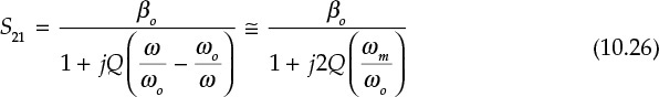
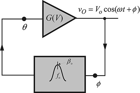
Figure 10.23 A simplified oscillator structure. The phase at the amplifier input is denoted by θ, while that of the amplifier output is denoted by ϕ.
where ωo represents the oscillation frequency and ωm = ω - ωo represents the offset frequency. Generally, the magnitude of the frequency response in Equation (10.26) is approximately constant, while the phase is approximated as a straight line that decreases linearly within the 3-dB angular bandwidth of BW = ωo/Q.
In the oscillator structure shown in Figure 10.23, the equivalent noise source N can be placed at the amplifier input; its frequency characteristic is shown in Figure 10.24. The F in Figure 10.24 represents the noise factor, which will be added to the oscillator signal.
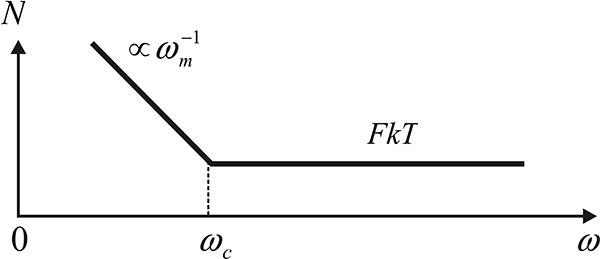
Figure 10.24 Noise at the amplifier input. The noise power at the amplifier input can be represented by FkT, which is explained in Chapter 4. At low frequency, the noise increases from FkT. The frequency ωc = 2πfc is called the corner frequency or flicker frequency.
Suppose that the oscillation signal is frequency-modulated by the noise signal shown in Figure 10.24 due to the nonlinearity of the amplifier. The frequency-modulated signal then appears at the output of the amplifier, which is the oscillator output signal. The peak frequency deviation of the frequency-modulated signal by the noise is denoted as Δω. Note that Δω is proportional to N shown in Figure 10.24. Then, the frequency-modulated signal is applied to the input of the feedback network, and the output of feedback network appears again at the input of the amplifier. When the oscillator output, which is frequency-modulated by the noise, is applied to the input of the feedback network, the frequency-modulated signal is transformed into a phase-modulated signal by the feedback network. The peak phase deviation Δθ of the phase-modulated signal is related to the peak frequency deviation as expressed in Equation (10.27).
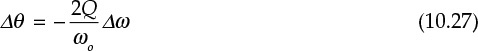
Thus, the phase-modulated signal with the peak phase deviation given by Equation (10.27) will appear at the input of the amplifier. Note that both Δω and Δθ are proportional to (N)½, shown in Figure 10.24. Since the peak phase deviation Δθ is proportional to (N)½, the single-sideband phase noise at the input of the amplifier can be plotted, as shown in Figure 10.25. Here, the carrier power at the amplifier input is denoted as P.
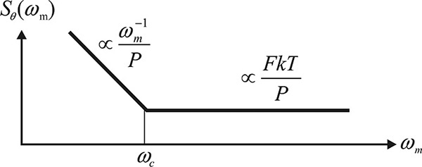
Figure 10.25 The phase noise at the amplifier input computed using the noise power shown in Figure 10.24
The phase noise of the amplifier input in Figure 10.25 can be written as Equation (10.28).
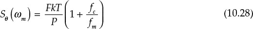
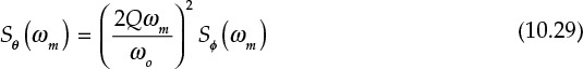
In addition, at the oscillator output, the peak frequency deviation Δω is related to the peak phase deviation Δϕ by Δω = ωmΔϕ. Using Equation (10.27), the relationship between the phase noise appearing at the amplifier input and the phase noise appearing at the oscillator output is expressed in Equation (10.29).
Also, outside the resonator bandwidth BW there is no such relationship, which is shown in Equation (10.30).
Therefore, combining Equations (10.29) and (10.30), the combined can be written as Equation (10.31).
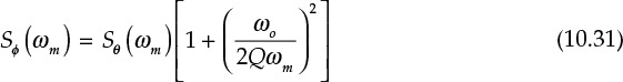
This is shown in Figure 10.26; that is, near the oscillation frequency, the phase noise decreases by ω–3 (30 dB/decade) and, after the 1/f noise disappears, the phase noise decreases by ω–2 (20 dB/decade). Then, outside the resonator’s bandwidth, it is proportional to the noise figure and shows a constant phase noise. It should also be noted that the higher the Q of the feedback network, the lower the phase noise.
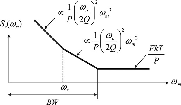
Figure 10.26 Phase noise of the oscillator. BW is the bandwidth of the feedback network. Outside the BW, the phase noise due to the white noise is given by FkT/P and it is increasing in proportion to ωm–2 inside BW. The phase noise further increases due to the flicker noise in proportion to ωm–3.
In conclusion, the phase noise S(fm) based on Leeson’s phase noise model can be expressed as
The Leeson’s phase noise model expressed in Equation (10.32) is an approximate description of phase noise. Note that the phase noise generation in an oscillator is basically a nonlinear phenomenon. However, the phase noise asymptotically approaches the Leeson’s phase noise model for higher fm. In addition, it should be noted that noise factor F of the amplifier in Equation (10.32) is seldom equal to the measured amplifier noise factor; for more information, see reference 3 at the end of this chapter. Noise factor F around the oscillation frequency is thought to be caused by the thermal noise and the DC bias-dependent shot noise. However, the DC bias-dependent shot noise generally becomes a function of the oscillating signal. As a result, it is modulated by the oscillating signal. Thus, it acts as a cyclostationary noise source in the oscillator, which makes F in Equation (10.32) differ from the measured amplifier noise figure. In addition, the flicker noise is also DC bias dependent and the flicker frequency fc in Equation (10.32) may also differ from the measured flicker frequency due to flicker-noise conversion dynamics. Recently, significant published research has focused on cyclostationary noises. However, a design for a low-phase noise oscillator to meet a given phase noise specification is still only a theory despite recent research on oscillator phase noises and the emergence of modern CAD simulators. We will present the experimental method to meet the design objective of the phase noise in the design of a DRO (dielectric resonator oscillator) in section 10.7.
The Leeson model is based on deduction and should be proven experimentally.3 The basic assumption is the frequency modulation by the noise at the amplifier input, namely the peak frequency deviation, is proportional to the noise frequency characteristic. This assumption has been experimentally verified by Pucel and Curtis, who measured the 1/f noise of the drain current of a GaAs FET under a given DC voltage. The fluctuation of the drain current ΔId2 observed with a spectrum analyzer is shown in Figure 10.27. Using the drain current fluctuation, the peak frequency deviation Δf2 of the oscillation output can be calculated. This peak frequency deviation is usually referred to as FM noise. In this case, the frequency dependence of the FM noise must be the same as that of the drain current noise since the FM noise is assumed to be proportional to the drain current noise. The measured and computed FM noises shown in Figure 10.27 are found to have the same frequency dependence as that of the drain current noise.
3. D. B. Leeson, “A Simple Model of Feedback Oscillator Noise Spectrum,” Proceedings of the IEEE 54, no. 2 (February 1966): 329–330.
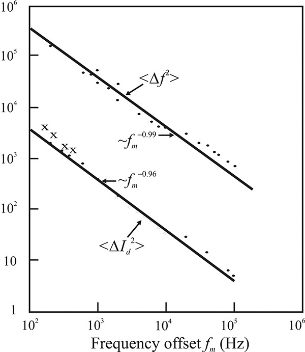
Figure 10.27 The Pucel experimental results of a GaAs FET 10-GHz oscillator phase noise.4 Baseband noise ΔId2 represents the measured drain current fluctuation in unit (nA2/Hz), while FM noise is measured in the unit (Hz2/Hz). Since the FM noise is directly proportional to the baseband noise as expressed in Equation (10.27), the FM noise should show the same dependence as in the baseband noise, and this clearly appears in the plot.
4. R. A. Pucel and J. Curtis, “Near-Carrier Noise in FET Oscillators,” IEEE MTT-S International Microwave Symposium Digest, (May 31–June 3, 1983): 282–284.
10.3.4 Comparison of Oscillator Phase Noises
It is often necessary to compare the performance of oscillators in terms of phase noise even though the oscillators generally have different oscillation frequencies. To compare the phase noises of two oscillators with different oscillation frequencies, the frequency of one oscillator must first be made equal to that of the other using frequency division or multiplication. First, we will examine the changes in phase noise resulting from frequency multiplication or division.
Suppose that the time-domain waveform of an oscillator is given by Equation (10.33).
Then, after the frequency multiplication by n, the resulting output waveform can be expressed with Equation (10.34).
Thus, the phase noise of the multiplied waveform can be expressed as Equation (10.35),
which represents a degradation of the phase noise by n2. As an example, the frequency of a 10-MHz crystal oscillator is multiplied by n = 1000 to give the frequency of 10 GHz. Since n = 1000, the phase noise increases by 60 dB.
In this way, the phase noises of various oscillators can be compared, as shown in Figure 10.28, where a crystal oscillator, a DRO (dielectric resonator oscillator), and a microstrip VCO (voltage-controlled oscillator) are graphed. Their oscillation frequencies are 10 MHz for the crystal oscillator, 1 GHz for the DRO, and 10 GHz for the microstrip VCO. The frequencies of the oscillators are first set to 10 GHz. Thus, the frequencies of the crystal oscillator and the DRO are multiplied by factors n = 1000 and 10, respectively. After the frequency multiplication, the phase noises are compared, as shown in Figure 10.28. From this figure, although the noise floor of the crystal oscillator is higher (as a result of multiplying the frequency by a factor of 1000), the phase noise at low frequency can be found to be the lowest compared to the other oscillators. This is followed by the DRO, and then the microstrip VCO, which has the poorest phase noise.
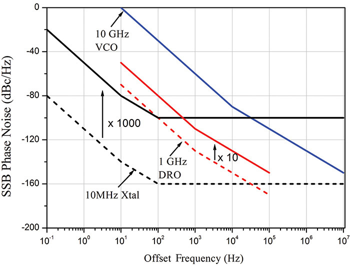
Figure 10.28 Comparison of the phase noises of various oscillators: a 10-MHz crystal oscillator, a 1-GHz DRO, and a 10-GHz VCO. All the frequencies are converted to the 10-GHz frequency.
At a 100-kHz frequency offset, a VCO with a center frequency of 10 GHz has a phase noise of -100 dBc/Hz, while another VCO with a center frequency of 35 GHz has a phase noise of -96 dBc/Hz. Compare the phase noises of the two oscillators.
Solution
To set the frequency of the 10-GHz VCO to 35 GHz, the required frequency multiplication factor is
The phase noise of the 10-GHz VCO after its frequency multiplication by n equals
Thus, the phase noise of the 10-GHz VCO is poorer than that of the 35-GHz VCO by 7 dB.
10.4 Basic Oscillator Circuits
10.4.1 Basic Oscillator Circuits
The possibility of oscillation for a given oscillator circuit was investigated in section 10.2. Now we will present the design of oscillator circuits that oscillate at a specified frequency. The design of an oscillator circuit can be carried out using basic oscillator circuits.
First, after removing the DC bias circuits and all the elements that have no effects at the RF in a given oscillator circuit, most oscillator circuits can be categorized into two configurations: series feedback oscillators, as shown in Figure 10.29, or parallel feedback oscillators, as shown in Figure 10.30. In Figure 10.29, the series feedback is achieved by jy, which delivers the transistor DS output to the GS input. In contrast, the parallel feedback shown in Figure 10.30 is achieved by jy, which delivers the DS output to the GS input. Three types of series feedback oscillator configurations and three types of parallel feedback oscillator configurations are shown in Figures 10.29 and 10.30, respectively.

Figure 10.29 Three series feedback oscillators. (a) The load is connected to the drain, (b) to the source, and (c) to the gate terminals.
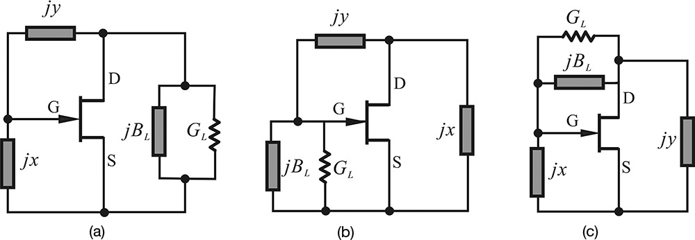
Figure 10.30 Three parallel feedback oscillators. (a) The load is connected to the drain, (b) to the gate terminals, and (c) to the feedback path.
The classifications for the three types of configurations in Figures 10.29 and 10.30 are based on where the loads are connected, whereas the feedback type can be found to be essentially the same for all three types. In addition, jx and jy in the figures represent the reactance of a capacitor or inductor in the series feedback configurations, while they represent the susceptance of a capacitor or inductor in the parallel feedback configurations.
The basic forms of the oscillator circuits in Figures 10.29 and 10.30 can be represented by an amplifier and a feedback network. The basic form of the series oscillator shown in Figure 10.29 can be converted into the T-type feedback network in Figure 10.31(a), and the basic form of the parallel feedback oscillator can be converted into the π-type feedback network in Figure 10.31(b).
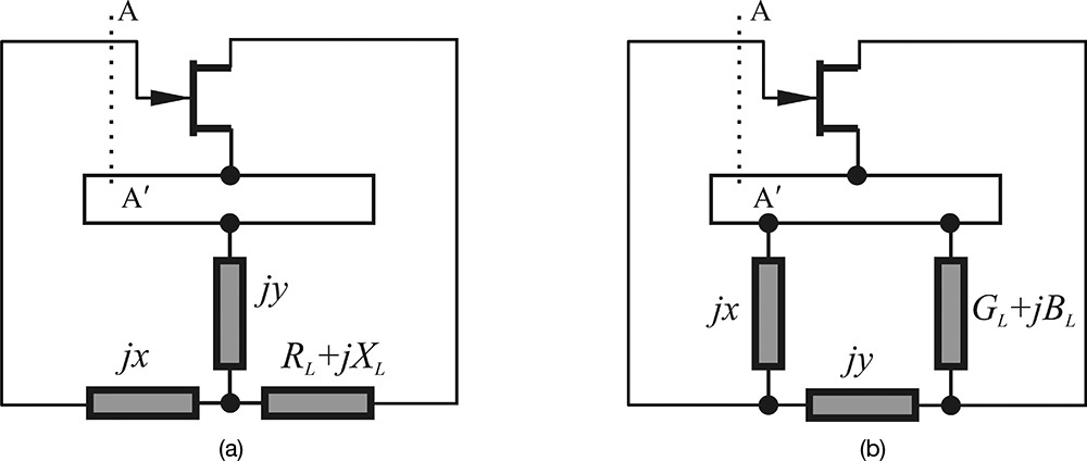
Figure 10.31 The conversion of the oscillator circuit into a feedback form. (a) T-type feedback network converted from the basic oscillator circuit in Figure 10.29(a) and (b) π-type feedback network converted from the parallel feedback oscillator in Figure 10.30(a)
The oscillation mechanism of the series or parallel configuration can be qualitatively understood by analyzing the feedback structure. First, for the series configuration of Figure 10.29(a), the reactance jx is replaced by capacitor C2, the feedback reactance jy is replaced by inductor L, and the load is replaced by a capacitor C1 and resistor r in series. In addition, since the input impedance of the transistor at high frequencies is generally low, by approximating it as short, the equivalent circuit of the transistor can be represented by a current-controlled voltage source, as shown in the shaded rectangle of Figure 10.32. The open-loop circuit can be obtained by cutting the FET input (the A–A’ reference plane in Figure 10.31) and reconfiguring the circuit. As the input impedance of the transistor is approximated as short, a shorted load can be connected where the cut occurs. To obtain the open-loop gain, a unit current source is applied to the transistor input of the open-loop circuit, which is shown in Figure 10.32. The open-loop gain is then the –Ir of Figure 10.32.

Figure 10.32 Open-loop circuit of the circuit in Figure 10.31(a). The gate-source plane is cut and the unit test current is applied.
Here, Equations (10.36a) and (10.36b) express the parallel impedance of L and C2.
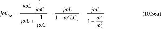
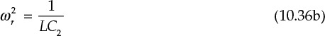
Thus, at frequencies lower than ωr, L and C2 in parallel are equivalently treated as an inductor Leq. In addition, since the current transfer function Ir/I becomes
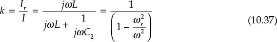
at frequencies lower than ωr, the phase of k becomes 180° and a phase inversion occurs, as expressed in Equation (10.37). In contrast, at frequencies higher than ωr, the phase becomes 0° and results in the disappearance of the phase inversion. It also is worth noting that k is a real number. In addition, the open-loop gain L is now expressed by Equations (10.38a) and (10.38b).
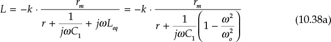
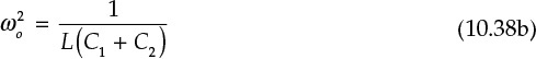
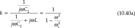
Since ωo < ωr, the open-loop gain is positive real at ω = ωo and therefore the phase of the open-loop gain is 0. The open-loop gain is
When the gain given by Equation (10.39) is greater than 1, oscillation can form. In the circuit, note that phase inversion occurs due to L||C2 and the oscillation frequency occurs at the resonant frequency of L||(C1 + C2). This is shown in Figure 10.33.

Figure 10.33 (a) Phase of k and (b) open-loop gain of the series feedback oscillator for the frequency
In the case of the parallel feedback oscillator in Figure 10.30(a), the oscillator circuit can be similarly implemented by replacing the reactance jx with a capacitor C2, the feedback reactance jy is replaced with an inductor L, and the load is replaced with a capacitor C1 and resistor R in parallel. Furthermore, the input impedance of the transistor at low frequencies is generally high; the equivalent circuit of the transistor can be approximately represented by a voltage-controlled current source, as shown in the shaded area of Figure 10.34. Similar to the previously discussed series-feedback-type oscillator, to obtain the open-loop gain, the circuit is cut at the transistor input and the open-loop circuit is drawn as shown in Figure 10.34, where a unit voltage source is applied to the input, and the open-loop gain is obtained by calculating the voltage Vr returning from the output to the input.
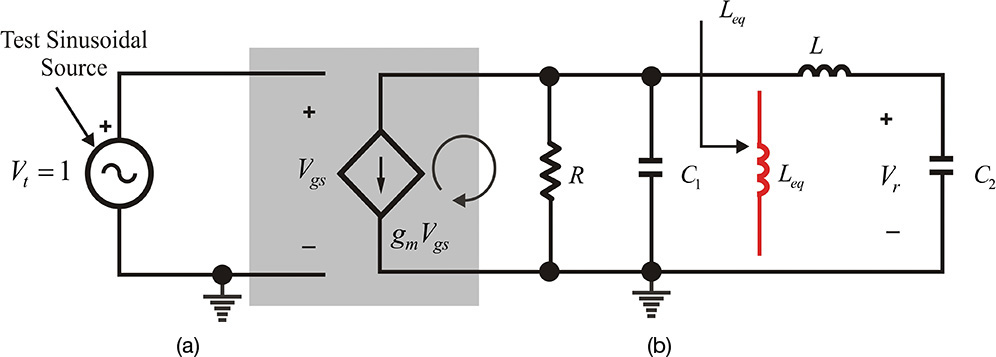
Figure 10.34 Circuit for calculating the open-loop gain of a parallel feedback oscillator circuit. The gate source in Figure 10.31(b) is cut and the test voltage is applied to calculate the open-loop gain.
From that figure, the voltage transfer function computed as k = Vr/Vo is given by Equations (10.40a) and (10.40b).
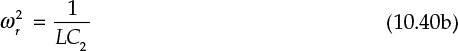
Thus, phase inversion appears for frequencies higher than ωr and disappears for frequencies lower than ωr. In addition, as in the case of series feedback, k is a real number. In addition, the open-loop gain is shown in Equations (10.41a) and (10.41b).
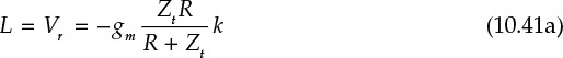
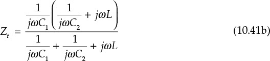
Thus, the open-loop gain is given by Equation (10.42).

Since the imaginary part of the denominator of the expression above must be 0 for oscillation to occur, the oscillation frequency
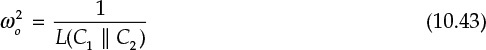
It can also be seen that ωo > ωr from Equations (10.40b) and (10.43). Substituting Equation (10.42) into the open-loop gain equation, the following condition must be satisfied for oscillation to occur:
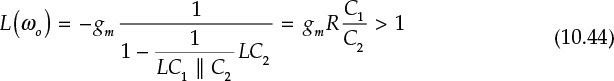
Thus, no oscillation occurs when the open-loop gain given by Equation (10.44) is less than 1. From that equation, the oscillation frequency is the resonant frequency of the overall LC resonant circuit seen from the output. Furthermore, since ωo > ωr, the value of k is found to be negative. That is, the oscillation frequency must always be higher than the frequency that causes the phase inversion. Because the amplifier is an inverting amplifier that has its own phase inversion of 180o, the k network should provide the phase inversion of 180o to restore the overall phase of the open-loop gain to 0º. This is shown in Figure 10.35.

Figure 10.35 (a) Phase of k and (b) open-loop gain of the parallel feedback oscillator for the frequency
10.4.2 Conversion to Basic Forms
The actual oscillator circuit is realized by applying DC voltage to the basic-form oscillator circuit that represents the equivalent circuit at the RF frequency. The actual oscillator circuit sometimes looks slightly different from the basic forms. However, most oscillators when simplified can be converted to the previously mentioned basic forms of the oscillator. Thus, for a given oscillator circuit, the design tasks first require the conversion of the oscillator circuit to one of the basic forms and then DC voltage must be applied to the selected basic form of the oscillator circuit. In this section, we will examine these tasks through some examples.
Figure 10E.15 represents a microstrip oscillator circuit. Simplify this circuit and convert it into the oscillator circuit’s basic form.

Solution
Removing the DC bias circuit portion of Figure 10E.15 results in the bottom-right circuit in Figure 10E.16.
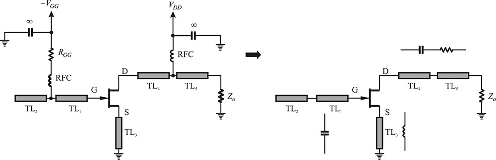
The circuit connected to the drain terminal can be seen as an RC series circuit at the oscillation frequency. Also, assuming the length of transmission line is short, the transmission line connected to the source can be seen as an inductor. In addition, the two transmission lines connected to the gate terminal can be considered as a capacitor and, by removing the ground, the microstrip oscillator circuit can be equivalently redrawn as the basic form of the series feedback oscillator in Figure 10.29(a).
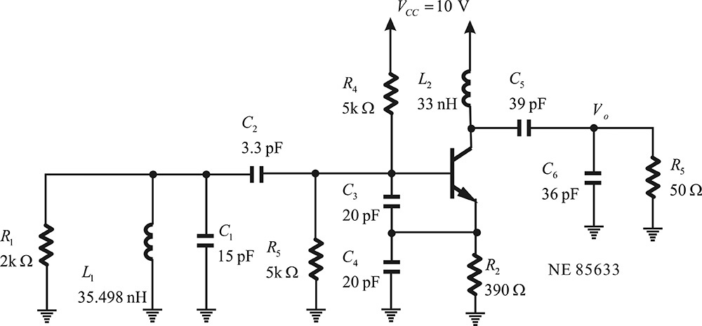
The circuit shown in Figure 10E.17 is a 200-MHz-band Colpitts oscillator.5 The S-parameters of transistor NE85633 at Vce = 3.5 V and Ic = 10 mA are used. Show that the circuit oscillates at 200 MHz using the open-loop gain. Then, using ADS, convert the circuit into a basic parallel feedback oscillator and calculate the values of the resulting admittance jx, jy and the load admittance GL + jBL at 200 MHz.
5. M. Randall and T. Hock, “General Oscillator Characterization Using Linear Open-Loop S-Parameters,” IEEE Transactions on Microwave Theory and Techniques 49, no. 6 (June 2001): 1094–1100.
Solution
After removing the ground point in Figure 10E.17 and moving the new ground to the transistor’s emitter, the S-parameter of NE85633 is inserted and simulated in ADS, as shown in Figure 10E.18, to confirm the open-loop gain at 200 MHz. To compute the open-loop gain, the oscillator feedback is cut at the base-emitter plane. Two ports are connected where the feedback loop is cut, as shown in Figure 10E.18.
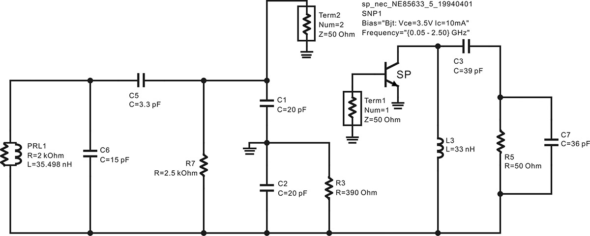
Figure 10E.18 Circuit for calculating the open-loop gain. The ground point is moved to the emitter and the oscillator is cut along the base emitter. After the breaking the loop, the oscillator circuit is redrawn. Note that the S-parameter data component for NE85633 is used.
After the S-parameter simulation, the equation in Measurement Expression 10E.3 is similarly entered in the display window to compute the open-loop gain G using the simulated S-parameters. The simulated open-loop gain G is shown in Figure 10E.19. From the phase of G, the oscillation condition is found to be satisfied at a frequency of approximately 200.9 MHz.
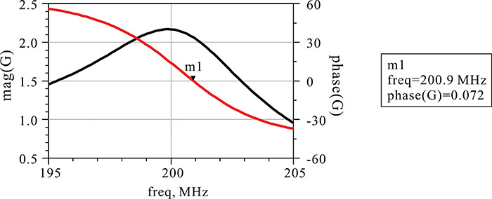
Figure 10E.19 Open-loop gain calculation result. The phase of the open-loop gain crosses 0 at about 200.9 MHz, at which |G| > 1 and the oscillation is possible.
The two-port parameter values of the oscillator circuit’s feedback network can be obtained by removing the transistor, as shown in Figure 10E.20. The two-port Y-parameters of the circuit shown in that figure can now be obtained. These parameters can be represented by the p-type circuit shown in Figure 10.31(b). Since it is a passive network, y11 + y12 corresponds to the admittance jx, and y22 + y12 corresponds to YL = GL + jBL, while jy corresponds to -y12 in the basic form of the parallel feedback oscillator. Therefore, the following equations shown in Measurement Expression 10E.4 are entered in the display window and the values of the admittances in Table 10E.1 are displayed in a list.
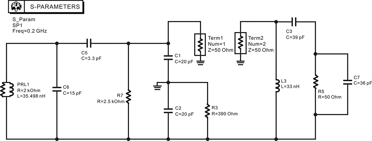
Figure 10E.20 Calculation of the two-port circuit parameters external to the oscillator. To obtain the Y-parameters of the feedback network, the BJT is removed and the Y-parameters are computed for the remaining network.
![]() jx=Y(1,1)+Y(1,2)
jx=Y(1,1)+Y(1,2)
![]() jy=-Y(1,2)
jy=-Y(1,2)
![]() YL=Y(2,2)+Y(1,2)
YL=Y(2,2)+Y(1,2)
Measurement Expression 10E.4 Equations for the feedback parameters x, y, and YL

In these equations, jy is an inductor and YL and jx are capacitors. However, note that jx and jy are not pure imaginary numbers because the collector terminal of the transistor in Figure 10E.18 is not connected to a ground but, instead, to a 33-nH inductor. Also note that the real part of jx is the largest and the load is connected to the base rather than the collector terminal.
For the basic parallel-type oscillator shown in Figure 10E.21, put the ground point at the collector and then implement the oscillator circuit by adding a DC bias.
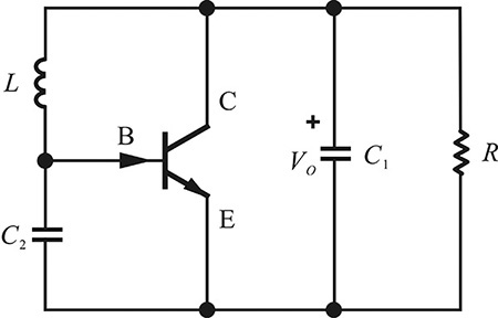
The oscillator circuit with the collector as a ground is called a Colpitts oscillator and it can be implemented as shown in Figure 10E.22.
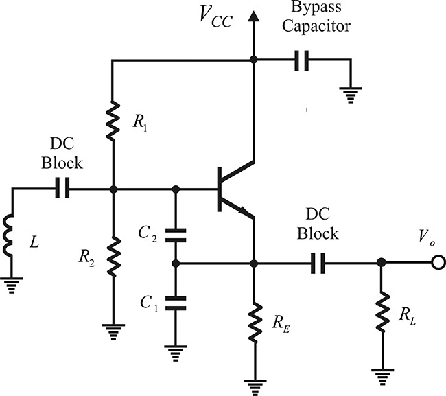
The collector DC voltage is supplied through the bypass capacitor and the oscillation output is obtained from the emitter terminal. The DC voltage to the base is supplied using the bias resistors R1 and R2. Furthermore, a DC block capacitor is inserted between the inductor and base to prevent the base from being grounded. The emitter current of the BJT can then be set by the resistor RE. In addition, the DC block capacitor is necessary to prevent the appearance of DC voltage at the output. The inserted resistors should provide higher impedances than those of the components around them at the oscillation frequency so as not to affect the RF signal at that oscillation frequency. The common collector implementation is easy and is thus widely used. The Colpitts oscillator circuits of Figures 10E.12 and 10E.17 are a type of common-collector oscillator circuit. In particular, in order to reduce the impact of the emitter bias resistor, the RFC may be used, as shown in Figure 10E.12. It should be noted that because the DC block capacitors and the RFCs inserted for the DC bias can be made to satisfy the oscillation conditions at other undesired frequencies, the appropriate values of the capacitors and the RFCs should be chosen so as not to satisfy the oscillation conditions at undesired frequencies. Instead of the common collector, the ground can be set as the emitter or the base. However, these kinds of configurations are not widely used due to the complexity of their implementations.
10.4.3 Design Method
Oscillator design from the impedance point of view is relatively simple; that is, the reference plane is set at the active part, which could be either Gunn or IMPATT diodes, and a series resonant load at the oscillation frequency is formed by adding a matching circuit to the 50-Ω load. The matching circuit must be designed such that the resistance looking into the load from the active part is smaller than the negative resistance of the active part. Alternatively, from the admittance point of view, a parallel resonant load is formed by adding a matching circuit to the 50-Ω load and the matching circuit must be designed such that the value of the parallel load is greater than the negative resistance of the active part.
The design concept from the impedance or admittance point of view can be similarly applied to the design of the series- or parallel-feedback-type oscillators. In the case of the series feedback type, the reference plane is set at the terminating reactance jx, as shown in Figure 10.36(a), and the active part is designed to satisfy the oscillation condition. For the purpose of simple design, the load ZL = RL + jXL is set as XL = 0, ZL = Zo, and the series feedback reactance jy that gives the appropriate negative resistance value can be found by varying jy. Now, denoting the impedance looking into the active part from the reference plane as Zin, the oscillation condition can be satisfied by setting the value of jx as x = –Im(Zin). Next, adding the DC bias circuits for the transistor completes the oscillator design. This design method is simple; however, when the gain of the transistor is not high, the negative resistance is not induced at the reference plane, which causes problems in oscillator design. In that case, the design can be accomplished by trial-and-error adjustment of the load impedance value ZL.
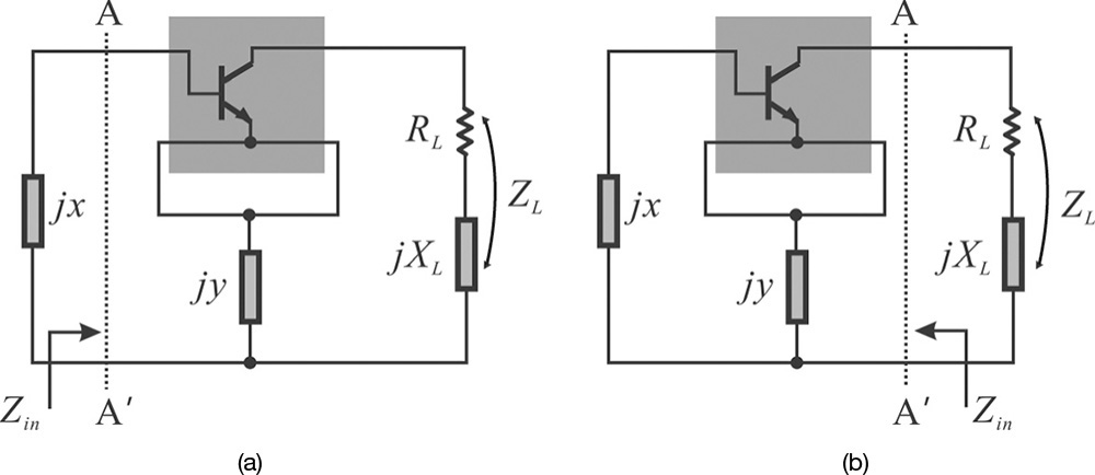
Figure 10.36 Design of a feedback-type oscillator: (a) jx reference plane and (b) load reference plane
Alternatively, the reference plane is set at the load, as shown in Figure 10.36(b).6 In addition, the reactance pair jx and jy are set to make the real part of the impedance Zin seen from the load ZL negative. The selection of jx and jy is possible when the contour of the real part of Zin is plotted in the (x, y) plane. The method of plotting these contours can be found in Appendix E and, by using this method, the (x, y) values giving negative resistance can be selected. Thus, for the selected (x, y) values, the impedance Zin seen from the load ZL can be calculated. The suitable load ZL for this Zin can then be synthesized using a matching network to satisfy the oscillation conditions. The real part of the load ZL must be less than the negative resistance of Zin, and ZL + Zin must be also designed to be series resonant at the oscillation frequency. The basic form of the parallel oscillator can be designed using both the admittance condition and a method similar to the design of the series oscillator’s basic form. This approach will be presented in the following section that deals with design examples. The mobile communication VCO will be designed following this approach.
6. M. Maeda, K. Kimura, and H. Kodera, “Design and Performance of X-Band Oscillators with GaAs Schottky-Gate Field-Effect Transistors,” IEEE Transactions on Microwave Theory and Techniques 23, no. 8 (August, 1975): 661–667.
The oscillator design based on the previously explained one-port method can easily determine oscillation frequency, but the determination of the oscillation frequency alone is not enough in designing an oscillator with two-port devices such as a transistor. For example, it will be impossible to know whether the transistor in the oscillator is set to give maximum gain or is set to give maximum output power. The oscillator design based on the two-port method can provide an improved design even though it is more complex than the one-port method.7
7. M. Q. Lee, S. J. Yi, S. Nam, Y. K. Kwon, and K. W. Yeom, “High-Efficiency Harmonic Loaded Oscillator with Low Bias Using a Nonlinear Design Approach,” IEEE Transactions on Microwave Theory and Techniques, 47, no. 9 (September 1999): 1670–1679.
First, consider the transistor shown in Figure 10.37 in an amplifier. For a given input power, the load impedance can be determined by the load-pull previously described in the power amplifier design in Chapter 9. The load impedance can be determined for maximum efficiency or for maximum output power. Then, the input voltage and current V1 and I1, and the output voltage and current V2 and I2 can also be determined. Using voltages and currents V1, V2 and I1, I2, the feedback network that yields V1 and I1 from the voltage and current V2 and I2 can be designed. The designed feedback network with the amplifier will form an oscillator that yields the designed frequency and output power of Posc = PL - Pin. Since a part of the output power PL is fed back to supply input power Pin in the oscillator circuit, Posc becomes PL – Pin.
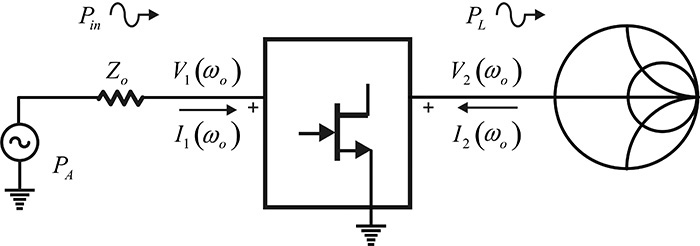
Figure 10.37 Determination of the input and output voltages and currents through the load-pull simulation
It is worth noting that the choice of the optimum source power level PA to give the maximum oscillation power is unknown. This requires the following iteration: for the chosen PA, the load impedance that maximizes PL can be determined through the conventional load pull. For the determined load impedance, PL - Pin can be plotted for PA. From the PL - Pin plot, the new optimum PA can be obtained. For that new PA, a new load impedance can be computed again through the load pull. Then, these steps are repeated to obtain the optimum load impedance that maximizes the oscillation output power.
Another problem can arise: In order to deliver the maximum input power to the input of the active device, the source and the input of the active device impedance must be conjugate matched. However, the large-signal input impedance of the active device is unknown until the load-pull simulation. Therefore, an initial value for the source impedance is determined using the small-signal S-parameters S11 and the load-pull simulation is then performed.
Using the determined voltages and currents V1, V2, I1, and I2, the feedback network should be designed to give the input and output voltages shown in Figure 10.38. With V1, V2, I1, and I2, the input power and oscillation output power are expressed in Equations (10.45a) and (10.45b).
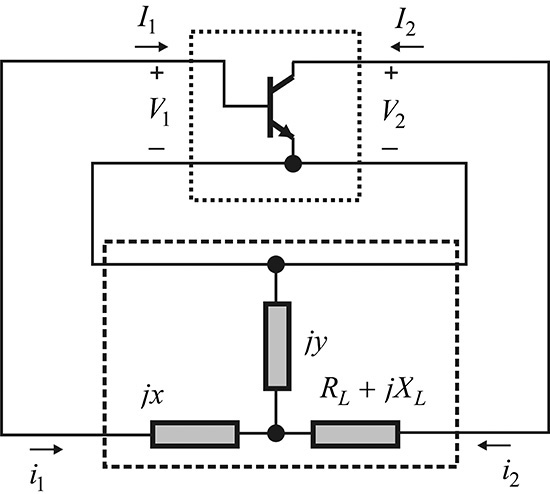
In addition, defining i1 = -I1 and i2 = -I2, as shown in the figure, and denoting the Z-parameters of the external feedback network as Ze, the terminal voltages V1, V2 can be expressed as Equation (10.46).
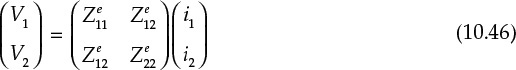
Now, Ze must be determined, because V1, V2, i1, and i2 have already been determined. The Z-parameters Ze for the T-type circuit are shown in Equations (10.47a)–(10.47c).
Thus, Ze has four unknowns that take the real and imaginary parts of ZL into consideration. Defining the new parameters expressed in Equations (10.48a)–(10.48d),
the values of x, y, and ZL can be determined as shown in Equations (10.49a)–(10.49c).
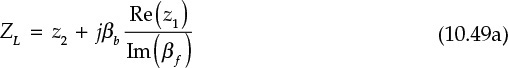
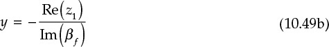
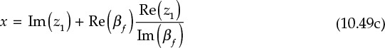
Similarly, in the case of a π-type feedback network, by defining the Y-parameters as Ye and following a similar process, the following parameters can be defined for the π-type feedback network, as expressed in Equations (10.50a)–(10.50d).
From these equations, the values for the feedback network can be determined with Equations (10.51a)–(10.51c) as follows:
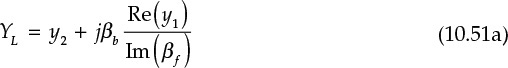
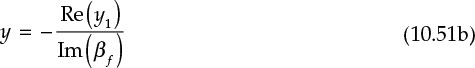
Note that the solutions for x, y, and ZL in Equation (10.49) make the open-loop gain equal to 1 at the large-signal condition. The gain at the maximum output power or large signal is generally lower than the small-signal gain. Thus, even when the open-loop gain is 1, the small-signal open-loop gain naturally becomes greater than 1 and does not cause major problems in oscillation start-up.
FHX35LG is a pHEMT and its large-signal model is available in the ADS library. The drain current IDS is about 4 mA at VDS = 2 V, VGS = -0.5 V. Design a self-bias circuit with a source resistor. Then, set up the load-pull simulation for the maximum oscillation power at the frequency of 2.5 GHz. Using the load-pull simulation results, determine the value of the series feedback network x, y, and ZL using Equations (10.48) and (10.49). Verify the series feedback network by simulating the oscillator built with the designed series feedback network.
Solution
VGS = -0.5 V is required for a drain current IDS = 4 mA. From this, VS should be 0.5 V when VG = 0. The value of the source resistance is thus Rs = 0.5/4 × 1000 = 125 Ω. This yields the source voltage of 0.5 V at a drain current of 4 mA. Since VDS = 2 V, a drain supply voltage should be 2.5 V. The self-bias circuit is shown in Figure 10E.23.
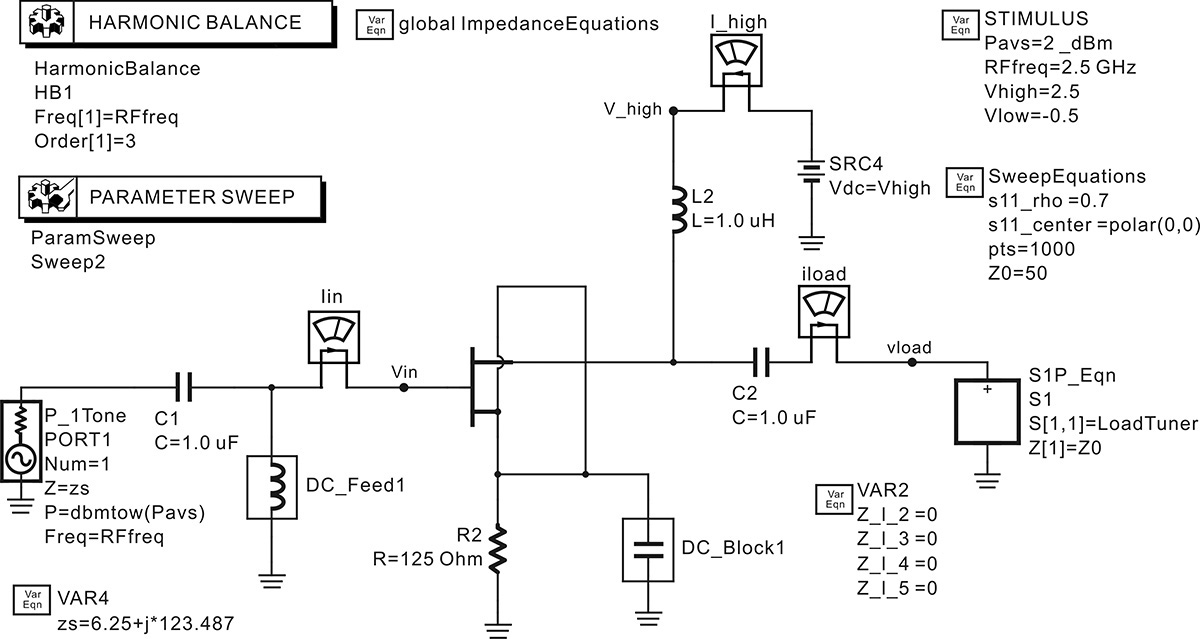
Figure 10E.23 Load-pull simulation schematic. The FET FHX35LG is self-biased to flow a drain current of 4 mA. The source impedance is determined to be the conjugate of S11. The harmonic impedances of the load are unknown and they are all set to 0.
The load-pull simulation circuit can be set up by modifying the load-pull schematic in section 9.3.2 of Chapter 9. The source impedance is set to the conjugate of S11. Its value is zs = 6.25 + j123.487 Ω. The harmonic impedances of the source should also be set to appropriate values. However, they are unknown and so all the harmonic impedance values are set to zs. The harmonic impedances of the load should also be appropriately set. All the harmonic impedances of the load from Z_l_2 to Z_l_5 are set to 0. Since the feedback network of the oscillator is a type of bandpass filter, the harmonic impedances can be approximated as short. Finally, the power level of the source must be set for the load-pull simulation. The source power level is initially set to 0 dBm. Figure 10E.24 shows the load-pull simulation results. From that figure, the maximum power level is about 7.95 dBm at the load impedance of 108.85 + j61.201 Ω.
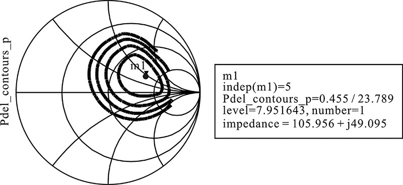
Figure 10E.24 Load-pull simulation results. At the load impedance of 105.956 + j49.095 Ω, the delivered power to the load is about 7.95 dBm.
Then, to plot Posc =PL - Pin, the simulation circuit shown in Figure 10E.25 is set up. To plot Posc = PL - Pin, the following equations in Measurement Expression 10E.5 are entered in the display window:
![]() PL_dBm=10*log(0.5*real(conj(vload[1])*iload.i[1]))+30
PL_dBm=10*log(0.5*real(conj(vload[1])*iload.i[1]))+30
![]() Pin_Watt=0.5*real(conj(Vin[1])*Iin.i[1])
Pin_Watt=0.5*real(conj(Vin[1])*Iin.i[1])
![]() Posc_dBm=10* log(0.5*real(conj(vload[1])*iload.i[1])-Pin_Watt)+30
Posc_dBm=10* log(0.5*real(conj(vload[1])*iload.i[1])-Pin_Watt)+30
Measurement Expression 10E.5 Equations for Posc = PL - Pin
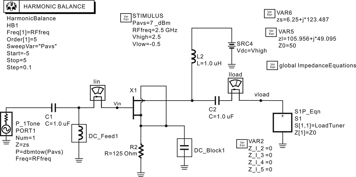
Figure 10E.25 Simulation schematic for determining the values of the oscillator’s series feedback network. Setting the load impedance that is determined from the load-pull simulation, the source power is varied to find the optimum oscillation power. The input and output voltages and currents at the optimum power are also computed to determine the oscillator feedback network.
Using the plot of Posc, the new source’s power level can be found. The 0 dBm source power that was initially chosen is now found not to yield maximum oscillation power. After iteration, the source power level is determined to be 2 dBm. Generally, the load impedance changes according to the change in the source power level. However, the load impedance is almost the same as that at the source power level of 0 dBm. The load impedance at the source power level of 2 dBm is found to be 105.956 + j49.095 Ω, which is shown in Figure 10E.25. The plot of the delivered power and oscillation power is shown in Figure 10E.26. The maximum oscillation power appears at the source power of 2 dBm and is 7.314 dBm. The delivered power to the load for Posc is 7.803 dBm.
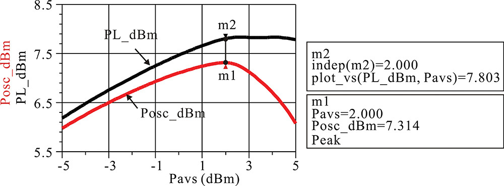
Figure 10E.26 Simulated PL and Posc. Posc = 7.314 dBm. At this power level, the values of the oscillator feedback network are determined.
To determine the series feedback network element values x, y, and ZL from the simulated output currents and voltages, the equations in Measurement Expressions 10E.6 and 10E.7 are entered in the display window. Measurement Expression 10E.6 is for the computation of the parameters z1, z2, βf, and βr in Equation (10.47). The index n in the first equation is the index of Pavs, which gives the maximum oscillation power. The outer index represents the harmonic number. Then, using the determined parameters z1, z2, βf, and βr from Measurement Expression 10E.6, the series feedback network element values of x, y, and ZL in Equation (10.48) can be determined by Measurement Expression 10E.7.
![]() n=find_index(HB.Pavs, indep(m1))
n=find_index(HB.Pavs, indep(m1))
![]() I2=-iload.i[n,1]
I2=-iload.i[n,1]
![]() I1=iin.i[n,1]
I1=iin.i[n,1]
![]() V1=Vin[n,1]
V1=Vin[n,1]
![]() V2=vload[n,1]
V2=vload[n,1]
![]() z1=-V1/I1
z1=-V1/I1
![]() z2=-V2/I2
z2=-V2/I2
![]() beta_f=(1+I2/I1)
beta_f=(1+I2/I1)
![]() beta_b=(1+I1/I2)
beta_b=(1+I1/I2)
Measurement Expression 10E.6 Equations for βf and βb
![]() ZL=z2+j*beta_b*real(z1)/imag(beta_f)
ZL=z2+j*beta_b*real(z1)/imag(beta_f)
![]() y=-real(z1)/imag(beta_f)
y=-real(z1)/imag(beta_f)
![]() x=imag(z1)+real(beta_f)*real(z1)/imag(beta_f)
x=imag(z1)+real(beta_f)*real(z1)/imag(beta_f)
Measurement Expression 10E.7 Equations for the feedback parameters x, y, and ZL
The computed results for x, y, and ZL are 143.76 Ω, -11.594 Ω, and 94.662 + j49.194 Ω, respectively. Figure 10E.27 shows the simulation schematic to verify the computed x, y, and ZL results.
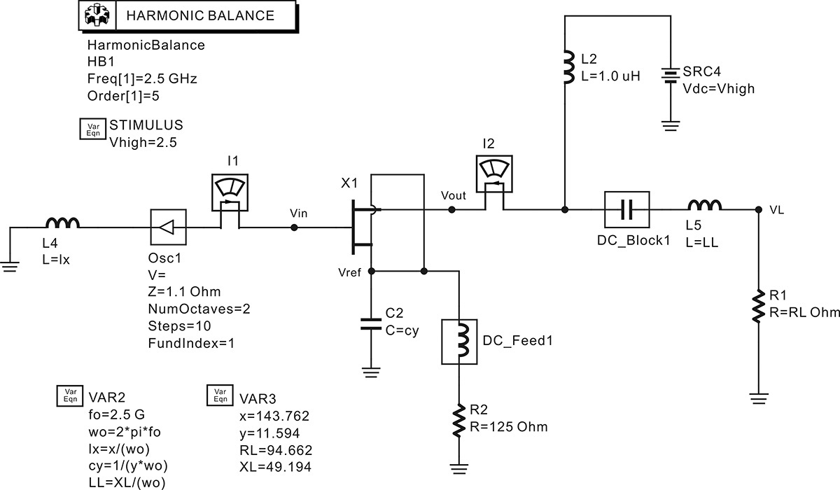
The simulated waveform and spectrum are shown in Figures 10E.28(a) and 10E.28(b). Figure 10E.28(a) is the simulated time-domain waveform of VL and Figure 10E.28(b) is the spectrum of VL. The oscillation output power is about 6.3 dBm. The value is less than the 7.3 dBm in Figure 10E.26. In addition, the oscillation frequency is 2.483 GHz, although it is close to 2.5 GHz. The difference in the oscillation power and frequency is due to the difference in the load impedances. The load impedance seen from the drain can be computed using (Vout - Vref)/(-I2). The harmonic impedances up to the three harmonics are computed as 105.962 + j47.695 Ω, 239.971 + j391.488 Ω, and 107.703 - j783.136 Ω, which are different from 94.662 + j49.194 Ω, 0 Ω, and 0 Ω. The differences of the harmonic impedances also make the drain voltage V2 in Figure 10.38 different. The ratio of V2 in the two simulations shown in Figure 10E.25 and Figure 10E.27 is about 1 dB, which explains the power difference of 1 dB. However, it can be seen that the result is fairly close to the expected value. It is possible to tune the values of x and y in order to obtain the exact oscillation frequency, but this tuning is not performed in this example.
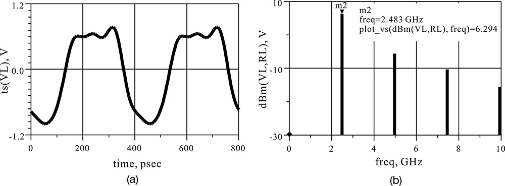
Figure 10E.28 (a) Oscillation waveform and (b) spectrum obtained through oscillator simulation. The oscillation power is smaller than the load-pull simulation given by 7.314 dBm. Note that the power is computed by dBm (VL, RL) because RL is not 50 Ω.
10.5 Oscillator Design Examples
10.5.1 VCO for Mobile Communications
Figure 10.39 shows the configuration of a voltage-controlled oscillator (VCO) used for mobile communications. The voltage-controlled oscillator has a size of 12 × 10 × 4 mm3, and a volume of approximately 4.8 cc. The smaller-size VCOs are still fabricated using the same technology shown in Figure 10.39. As can be seen in that figure, the VCO is composed of a metallic cover and a multilayer printed circuit board that is used to mount chip components. The metallic cover provides both electromagnetic shielding and ground. Therefore, the total weight of the VCO is determined by the multilayer printed circuit board and the thin metal cover, which makes the VCO lightweight. In addition, the terminals for DC power supply, oscillator output, ground, and frequency tuning for the VCO are formed by cutting in half the center of the multilayer printed circuit board’s through hole, which results in the half-plated cylindrical terminals. With the exception of the connection terminals, the bottom of the circuit board is coated with solder-resistant material. This provides electrical isolation and makes it possible for the PCB’s lines to pass through the bottom of the VCO when the VCO is mounted on the PCB.
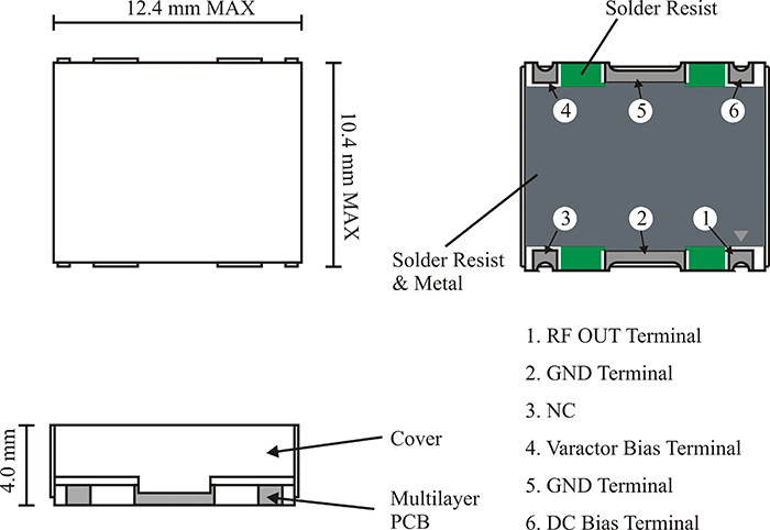
Figure 10.40 shows a cross-section of the multilayer PCB. The substrate is composed of three dielectric sheets of FR4 and the total thickness is 1.0 mm. Each dielectric has equal thickness. The first metal layer is for mounting components and the second metal layer is the ground for the first layer. The third metal layer is used for the RFC, strip-line resonator, and connection lines. The fourth metal layer is also the ground. Thus, the lines on the first layer are considered microstrip lines from the electromagnetic point of view, and the lines on the third layer become strip lines since they are surrounded by the ground planes. Note that except for the connecting holes, the lines on the first and third layers are electromagnetically isolated due to the second and fourth layers.
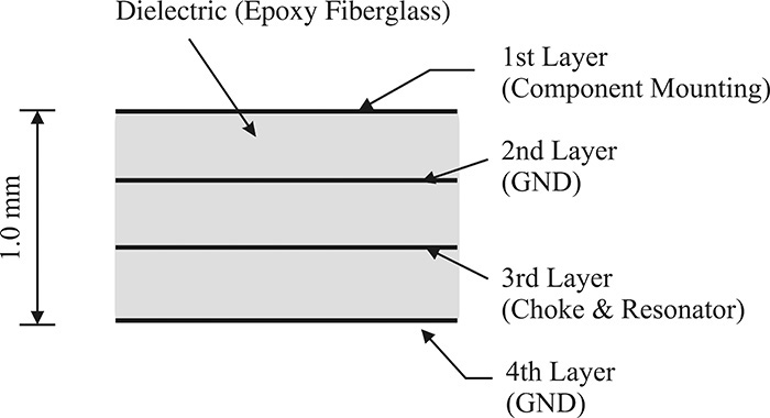
Figure 10.40 Configuration of a multilayer printed circuit board. Chip components are mounted on the first layer and the second layer acts as the ground for the first layer. Thus, the line on the first layer acts as a microstrip. The third layer is for the resonator and RFC, and the fourth layer is the ground. As a result, the lines on the third layer act as strip lines.
The VCO circuit used here is shown in Figure 10.41, where two transistors, Q1 and Q2, are connected in cascade. Transistors Q1 and Q2 share a common emitter current and the VCO consumes only about one-half of the DC current compared with other VCOs not using cascaded structures. However, a relatively low DC voltage is assigned between the collector emitter of transistors Q1 and Q2, and a low RF output power as well as significant distortions can occur, which is a disadvantage.

In Figure 10.41, resistors R1, R2, and R3 determine the DC base voltages of Q1 and Q2. Supply voltage is divided by resistors R1, R2, and R3. The DC voltage across resistor R3 is applied to the base of transistor Q1. From this DC base voltage, the emitter current of transistor Q1 can be controlled by varying the value of resistor RE. In addition, the emitter current of Q2 is equal to that of transistor Q1. As the impedances of resistors R1, R2, and R3 can be set higher than those of their surrounding components, their effects can be ignored at the oscillation frequency. Generally, in the frequency band of operation (800 MHz–2 GHz), the Q of a chip capacitor is generally higher than that of an inductor. Also, because of their small sizes, chip capacitors are primarily used to construct VCOs. An inductor is used for the RFC and a resonator is implemented using a shorted transmission line. The collector of transistor Q1 is connected to the ground through a bypass capacitor CB2, and the transistor Q1 operates as a common collector. The capacitor CE is a feedback capacitor that yields a negative resistance. When the value of the feedback capacitor CE is small, only the resistor RE is left at the emitter of Q1, which becomes a negative feedback circuit consisting of resistor RE. As a result, the negative resistance disappears. In addition, when the value of CE is too large, capacitor CE operates as a short. Thus, transistor Q1 operates as a common emitter and negative resistance is not induced. As a result, in order to induce negative resistance, the value of the feedback capacitor CE must be appropriate at the oscillation frequency. To select an appropriate value for CE, ignoring RE and Cc2, the impedance Zt looking into the base of the transistor Q1 can be written as Equation (10.52).

Here, Cbe1 and gm1 represent the base-emitter capacitance and transconductance of Q1. Oscillation is possible due to the induced negative resistance given in this equation.
The oscillation output appears across capacitor CE, which is applied to the base of transistor Q2 through capacitor Cc2. The transistor Q2 operates as a common emitter amplifier due to the bypass capacitor CB2. Thus, the oscillation output that appears across capacitor CE is amplified by transistor Q2, which is then delivered to the load. Chip inductor L1 connected to the collector of the transistor Q2 is an RFC and capacitors Cm1, Cm2 are for matching, which aims the maximum power delivery to the load. Thus, CE is set to generate a negative resistance at the operating frequency. Note that capacitor Cc2, connected to the input of transistor Q2, appears in parallel to CE and the contribution of Cc2 should be considered in the determination of CE. The lower the value of Cc2, the lower the power delivered to transistor Q2. In contrast, the larger the value of Cc2, the larger the power delivered to Q2; however, it causes distorted output to appear at the load.
The resonator in Figure 10.41 is composed of a shorted transmission line TL1, a capacitor Ct, and a varactor diode. The resonant frequency of the resonator is tuned through a varactor diode, whose tuning range is limited by Ct in series. Thus, the oscillation frequency’s tuning range can be adjusted by controlling capacitor Ct. The oscillation frequency tuning range is reduced compared with the direct oscillation frequency tuning using the varactor diode alone, but the Q of the resonator becomes higher due to Ct.
Capacitor Cc1 is added in series to the base of the transistor Q1, and the imaginary part of the impedance generated by the feedback capacitor CE can be changed. This makes it easy to tune out the inductance of the resonator at the oscillation frequency. As a result, the resonator and active part can be in series resonance at the oscillation frequency.
In summary, the function of the capacitor Ct is related to the oscillation frequency’s tuning range, the capacitors Cc1 and CE are associated with the oscillation formation, and Cc2 is related to the coupling of the oscillation power and delivery to the amplifier. Capacitor Cc1 and inductor TL1 determine the oscillation frequency of the oscillator. In particular, by varying the value of inductor TL1, it is possible, to some extent, to easily adjust the center of the frequency tuning range. Obviously, capacitor Cc1 does not change the negative resistance as it is connected in series but, when the impedance of the active part is converted to the admittance through series-to-parallel conversion, Cc1 gives a variation of negative conductance. Thus, by adjusting capacitor Cc1, the oscillation may disappear. Therefore, TL1 is efficient for tuning the oscillation center frequency; however, it is difficult to tune once fabricated. Sometimes, by connecting a small tunable patch pattern in parallel with TL1, an adjustment to the inductor value of TL1 is possible and the center of the frequency tuning range can be tuned to some extent.
Most of the capacitor values explained above are implemented using chip capacitors that are mounted on the PCB during fabrication and it is easy to modify their values. Thus, the exact values of the length and width of the lines are not required as they would be in the design of a microstrip oscillator. Therefore, to design the VCO for mobile communications, the function of each component should be understood and the range of values that satisfy the given specifications should be found through design or simulation.
Table 10.1 provides brief specifications of the VCO for mobile communications. The transistor 2SC4226 from NEC is adopted.
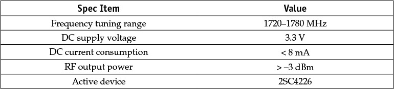
To design a VCO for mobile communications that satisfies the specifications above, the DC bias must first be set. The circuit of the active part is set up as shown in Figure 10.42 to determine the DC bias. All the capacitors used are implemented as chip capacitors and all the chip capacitors are replaced by a series RLC-equivalent circuit to include the parasitic components described in Chapter 2. In Figure 10.42, from a 3.3 V power supply, the base voltage of the oscillating transistor Q2 is
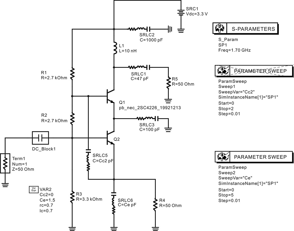
Figure 10.42 Simulation circuit for determining Ce and Cc2. First, the S-parameter simulation is performed at a fixed frequency of 1.7 GHz for the change of Ce, which is swept by Sweep2. The optimum value of Ce is determined from the Ce sweep. After the determination of the value of Ce, the value of Cc2 is then swept by Sweep1.
Thus, the emitter current is
The value of 11 mA is close to that of the DC current specification in Table 10.1. The exact value is determined through DC simulation. The calculated DC collector current is computed to be 6.45 mA at a supply voltage of 3.3 V. The resulting supply current is 6.83 mA, which satisfies the goal of 8 mA in Table 10.1.
Next, in order to operate the oscillating transistor (transistor Q2) in the common collector mode, the value of the DC block capacitor SRLC3 is set to 100 pF. The value of the bypass capacitor SRLC2 is set to 1000 pF. The value of the RF-output DC block capacitor SRLC1 is set to 47 pF, and no output matching circuit is used. In addition, RFC L1 is determined to be a 10-nH chip inductor (approximately 100 Ω at the oscillation frequency).
As mentioned earlier, the impedance Z = R + jX seen from port 1 should have negative resistance, and it is determined by the feedback capacitor Ce and coupling capacitor Cc2. To determine their values, first Cc2 is set to 0 and the impedance is calculated by varying Ce. The coupling capacitor Cc1 is replaced by the DC block and Z is plotted with respect to Ce.
The computed real and imaginary parts of Z are shown in Figure 10.43(a). The negative peak value of R occurs for Ce = 1.95 pF. To take the loading effect of Cc2 into consideration, Ce is initially set to 1.5 pF smaller than 1.95 pF and Cc2 is varied. As the value of Cc2 increases, the magnitude of R is reduced, as shown in Figure 10.43(b). Thus, Cc2 is set at 1.2 pF because the value of R begins to increase at the onset of 1.2 pF. The value of Cc2 is the maximum value that preserves the value of R determined by Ce. The maximum value of Cc2 is chosen to deliver the sufficient oscillation output power to the load. Note that the delivered power to the load is smaller for the smaller value of Cc2.
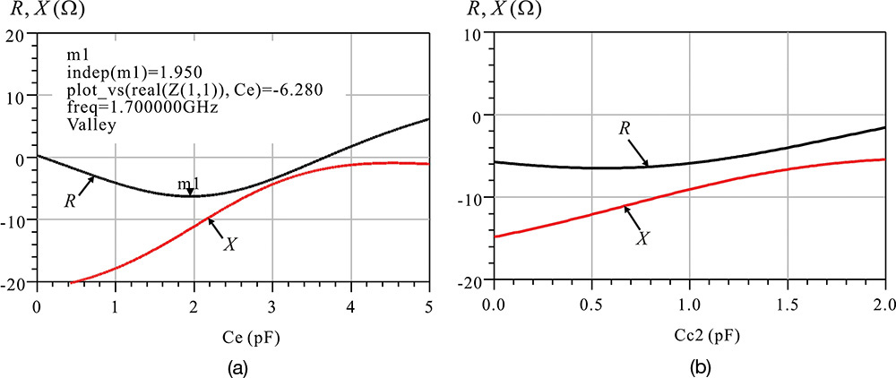
Figure 10.43 Simulated input impedance of the active part with Ce and Cc2 values as parameters. (a) The input impedance for Ce sweep; the negative resistance is maximum at Ce = 1.95 pF. (b) The input impedance for Cc2 sweep with fixed Ce; the value of Ce is determined to be 1.5 pF and Cc2 is swept. The value of Cc2 is determined to be 1.2 pF at the onset of the increasing resistance.
Next, a circuit must be set up to determine the oscillation frequency tuning range for the selected values of Ce and Cc2. The smv1235-079 varactor diode was used. The equivalent circuit of the smv1235-079 varactor diode is shown in Figure 10.44. Note that as the capacitance of the varactor diode at 0 V is large, the varactor diode will actually operate as a variable inductor. The equivalent circuit in Figure 10.44 is configured as a subcircuit. The oscillator circuit shown in Figure 10.45 is set up to determine the oscillation frequency tuning range.
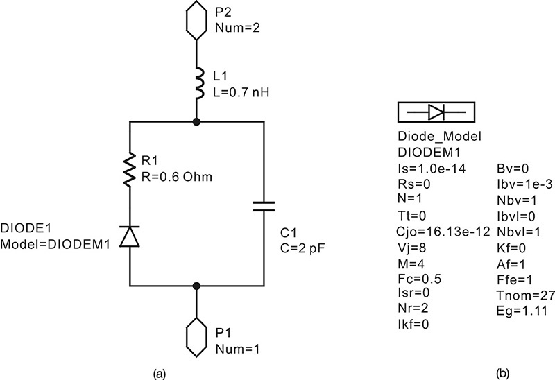
Figure 10.44 The equivalent circuit of the smv1235-079 varactor diode. Other diode parameters are not given and they are hidden.
As shown in Figure 10.45, the inductor in the resonator is set to 0.8 nH. The tuning voltage of the varactor diode is changed from 0 to 3.3 V, and the values of capacitors Cc1 and Ct are then adjusted. The oscillation center frequency is moved using Cc1 and the oscillation frequency tuning range is adjusted using Ct. Using the adjustment, the value of Cc1 is set to 4.7 pF and Ct is set to 3.9 pF. Figure 10.46 shows the simulated oscillation conditions using OscTest as well as the magnitude and phase changes of S11 with respect to frequency. From S11, the frequency tuning range is about 1.70–1.77 GHz, which is found to meet the specifications.
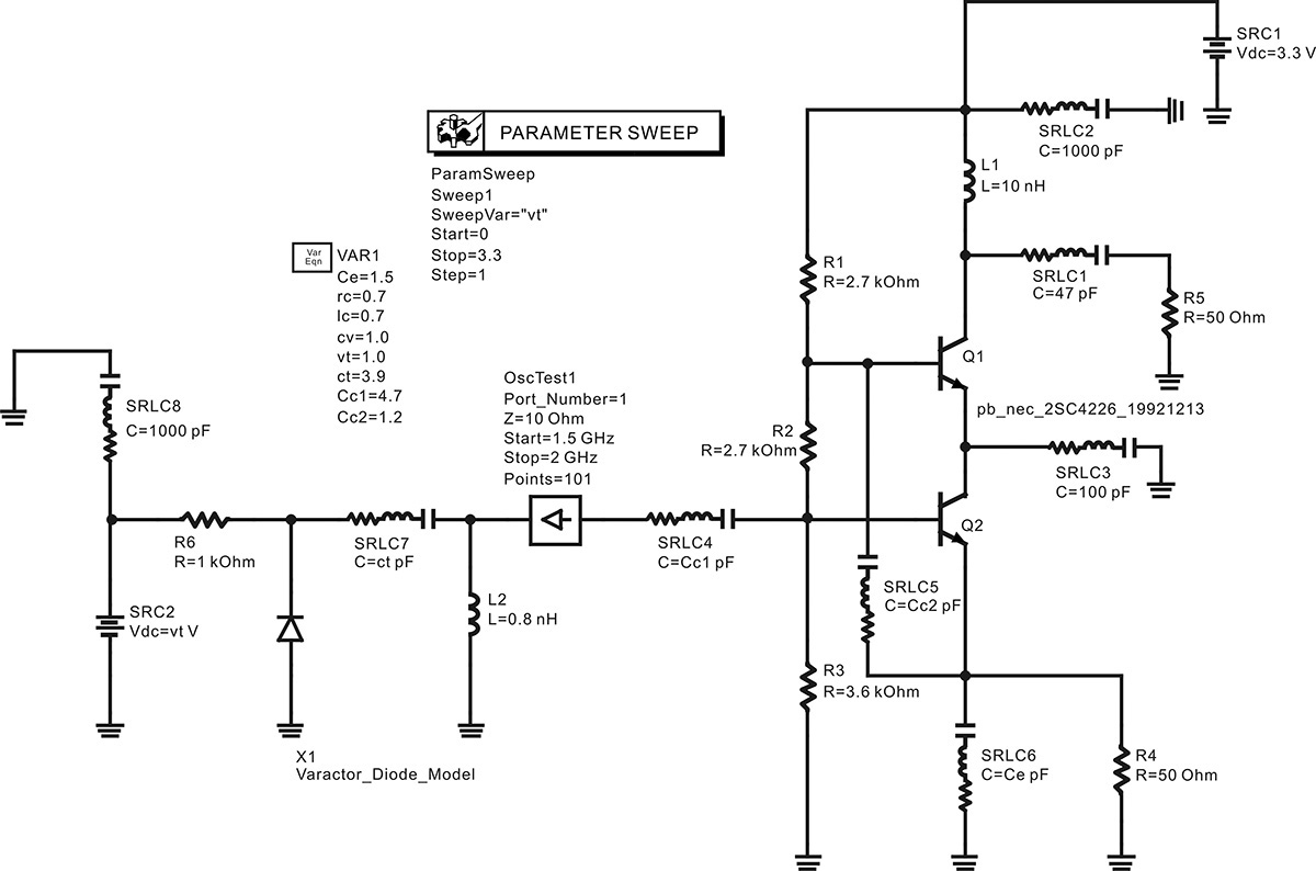
Figure 10.45 A VCO circuit for the simulation of the oscillation frequency’s tuning range. L2 is the resonator and is set 0.8 nH. The subcircuit X1 is the varactor diode that is shown in Figure 10.44. The capacitor Ct is used to tune the oscillation frequency’s tuning range.
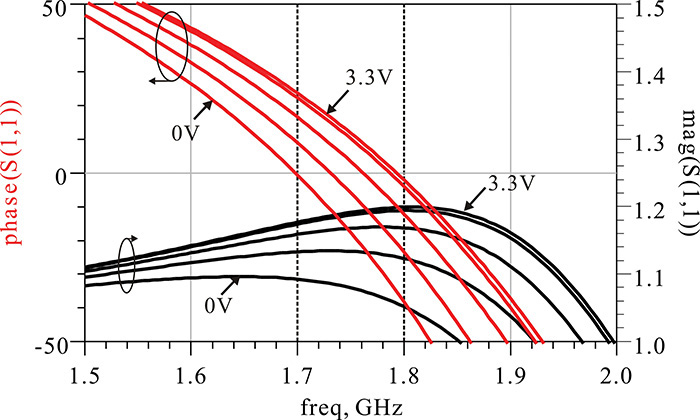
Figure 10.46 Frequency tuning range of the VCO circuit. The phase of S11 crosses 0 at a frequency range of 1.7–1.8 GHz and its |S11| > 1, which provides the oscillation frequency tuning range of 1.7–1.8 GHz.
Using the small-signal simulation, oscillation is found to occur and it covers the specified oscillation frequency’s tuning range. Next, the circuit shown in Figure 10.47 is built up and large-signal simulation is performed in order to determine the output power and frequency tuning range. The simulated oscillation frequency and power of the circuit are shown in Figure 10.48, where the output power range of -1.698 to -0.690 dBm is observed, which meets the desired specifications. The tuning voltage range of Vt that covers the desired oscillation frequency tuning range is approximately 0.6–2.8 V, as shown in Figure 10.48.
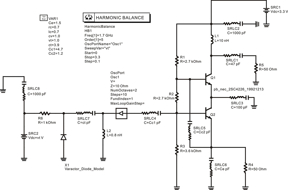
Figure 10.47 Circuit for a large-signal simulation. The OscTest in Figure 10.45 is replaced by OscPort for large-signal simulation.
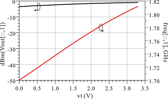
Figure 10.48 Oscillation frequency and output power variation with respect to tuning voltage Vt. The output power is about -3 dBm–0 dBm for the Vt change. The oscillation frequency changes from 1.70 to above 1.80 GHz for the Vt change.
In Figure 10.49(a), the time-domain waveforms are shown with the tuning voltage Vt as a parameter and the output waveform can be seen to be close to a sinusoidal waveform. The spectra of the oscillation waveforms are shown in Figure 10.49(b) and the second harmonic is found to be suppressed by approximately -20 dBc compared with the fundamental frequency.
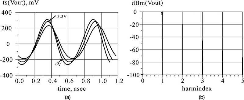
10.5.2 Microstrip Oscillator
The technique used in the design of the VCO for mobile communications described earlier is useful when components can be easily connected and removed by soldering. Since soldering can readily adjust the values of the components, the exact values of the components are not required in the design stage. Throughout the design stage, the designer should identify the role of each component and confirm that the oscillator’s fabrication will meet specifications. However, since the microstrip oscillator we will describe in this section is primarily composed of microstrip lines, it is not as easy to adjust those lines as it is in the mobile communications VCO. Thus, the exact dimensions of the microstrip lines are necessary in the design of a microstrip oscillator.
The microstrip oscillator can be designed using the impedance method in the design of the VCO for mobile communications described in the previous section. However, in this section we will demonstrate the design using the method from Example 10.13. The transistor employed for the design is a packaged pHEMT, FHX35LG (LG means low parasitic, hermetically sealed metal-ceramic package) shown in Figure 10.50. The large-signal model of the transistor is available in the ADS library. This section addresses the design of the oscillator using the large-signal model of the FHX35LG. Thus, the design can include both the oscillation frequency and the power. Typically, the large-signal model shows some errors, as discussed in Chapter 5, and these errors become larger as the frequency increases. Taking into consideration the error of the large-signal model, the oscillation frequency is set at 2.5 GHz, which is relatively low.
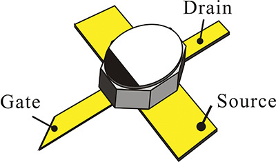
Figure 10.50 FHX35LG transistor package8
8. Fujitsu, FHX35LG/LP Super Low Noise HEMT, July, 1999.
10.5.2.1 Implementation of Microstrip Oscillator
The oscillator circuit shown in Figure 10E.27 in Example 10.13 is implemented using lumped elements such as inductors and capacitors. Therefore, to complete the microstrip oscillator, the lumped elements of Figure 10E.27 must be replaced with microstrip circuits that give the same impedance values at the oscillation frequency.
Figure 10.51(a) shows a microstrip circuit for replacing the inductor connected to the gate. The selected substrate has a thickness of 20 mil, a dielectric constant of 2.5, a loss tangent 0.0019, and a conductor thickness of 17.5 μm; the diameter of the via is fixed at 0.5 mm. To replace the inductor with a microstrip yielding the same impedance, the length of TL1, l1 is varied to obtain the same inductance value as that of the inductor. Taking the gate lead width of the package in Figure 10.50 into consideration, the width of TL1 is fixed at 0.8 mm. Figure 10.51(b) shows the result of the simulation. S11 represents the reflection coefficient with respect to the change of l1, and S22 is the reflection coefficient of the gate inductor lx. Thus, in Figure 10.51(b), the length l1 that gives the same value of reflection coefficient can be seen to be l1 = 14.88 mm.
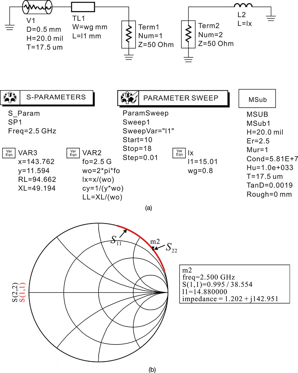
Figure 10.51 (a) The schematic for determining the microstrip length that gives the same impedance as the inductor and (b) simulation results. The length of about 14.88 mm gives the same impedance.
Figure 10.52(a) is a microstrip circuit implementation of the capacitor cy that is connected to the source terminal. The selected FHX35LG device has two source terminals. Thus, the capacitor cy in Figure 10.52(a) is configured as the parallel combination of the two microstrip circuits shown in that figure. In addition, the microstrip width is set wider than the width of the source terminal whose value is set to 1.2 mm. A self-bias circuit must also be included, but only in one circuit of the parallel combination. The point where the self-bias is connected is set 3.0 mm away from the source terminal. Note that the impedance seen from port 1 is not affected by the self-bias circuit at the oscillation frequency of 2.5 GHz. The two open microstrip stubs have almost the same impedances at 2.5 GHz because the lengths of those stubs are set to have equal lengths, l2. The length l2 is adjusted to make the impedance of the parallel combination equal to the impedance of cy.
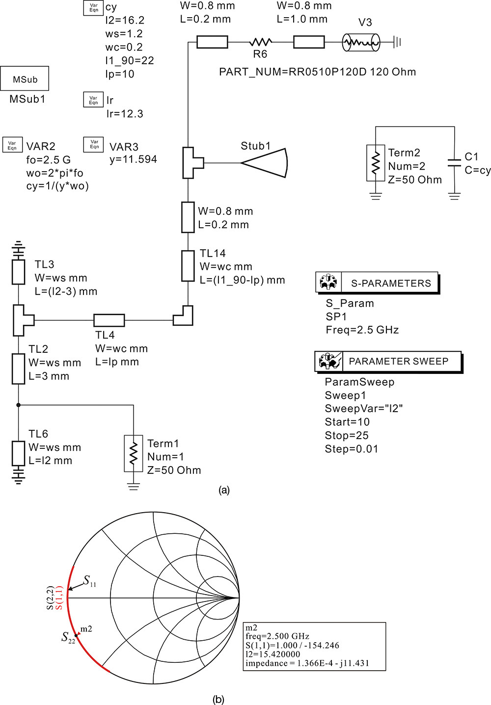
Figure 10.52 (a) Microstrip circuit implementation of the feedback capacitor and (b) simulation results. The length 15.42 mm gives the impedance of cy. In (a), TL2, TL3, and TL6 are the two stubs to implement cy, while other elements are the RFC and bias circuit elements. The radial stub length lr = 12.3 mm is determined using the separate simulation.
The RFC connected to the source terminal for the DC bias consists of a high-impedance microstrip with a length of about a quarter-wavelength and a radial stub. The width of the input terminal and angle of the radial stub are initially fixed at 0.8 mm and 70°, respectively. With the fixed width and angle, the length of the radial stub is set by separately simulating the radial stub’s impedance to make the input impedance 0 at 2.5 GHz. The length is calculated to be 12.3 mm. The width of the high-impedance microstrip operating as the RFC is set to 0.2 mm, and the length is set such that its electrical length is 90° at 2.5 GHz. The value is the l1_90 in Figure 10.52(a), which when computed with LineCalc is determined to be approximately 22 mm. The RFC microstrip line is bent at 90° to make the DC biasing easy while maintaining the value of the length l1_90. The shape is shown in Figure 10.52(a). In addition, the resistor used in the DC bias is implemented with a chip resistor from the ADS library, and the 120-Ω value is selected because the determined value of 125 Ω is not available in the ADS library. The simulation is performed by varying the length l2 and its results are shown in Figure 10.52(b). From that figure, when l2 = 15.42 mm, the impedance of the parallel combination is the same as that of the capacitor cy.
In the case of the load circuit, the impedance seen from the drain terminal should be implemented to have the impedance ZL = 94.662 + j49.194 Ω. This requires the synthesis of a matching network to transform the 50-Ω load into ZL. In addition, the load circuit must be implemented to include the DC block and DC supply circuit shown in Figure 10.53. Conceptually, this circuit can be configured by inserting a shunt inductor, as shown in Figure 10.53(a), where the inductor can be formed by connecting a bypass capacitor at the end of the high-impedance transmission line as shown in that figure. Thus, the DC supply can be applied through the bypass capacitor and the design of a separate DC supply circuit is not required. The DC block capacitor is implemented with a 100-pF chip capacitor. As explained in Chapter 2, the chip capacitor is not a pure capacitor. However, in order to show the operation of the circuit in Figure 10.53(a), the impedance of the chip capacitor is approximated to 0. When the impedance of the 100-pF DC block chip capacitor is considered to be 0, the shunt inductor moves the 50-Ω load at the origin of point B, as shown in Figure 10.53(b). The impedance at position B is then moved into the point of ZL through the clockwise rotation of the 50-Ω transmission line. The load circuit can then be implemented using the circuit shown in Figure 10.53(a).
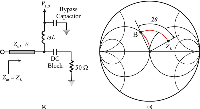
Figure 10.53 (a) Implementation of the load circuit and (b) matching in the Smith chart. Inductor L is used as a matching circuit element and it can also supply drain current at the same time. ZL is the desired impedance and it can be obtained by moving 50 Ω to point B by ωL and rotating B to ZL by the 50-Ω transmission line. In the matching, the DC block and bypass capacitors are assumed to be ideal.
Figure 10.54(a) shows the load circuit implemented with microstrip lines. The bypass capacitor for the DC power supply is implemented with a radial stub and a 100-pF chip capacitor. The radial stub has the dimensions used in the implementation of cy. In addition, a 100pF-chip capacitor is connected in parallel for the DC power supply. A microstrip with a width of 0.2 mm is used for the shunt inductor with a length of ll3 that is varied to provide the appropriate inductor value. The microstrip line is bent to minimize possible unwanted coupling to the cy circuit. The width of the 50-Ω microstrip is approximately 1.4 mm and its length is set to ll1 for optimization. A variable-length 50-Ω microstrip can also be inserted in front of the DC block chip capacitor. The length of this microstrip ll2 is optimized together with ll1 and ll3. Figure 10.54(b) shows the optimized impedance for the optimized dimensions shown in Figure 10.54(a). The impedance can be seen to be close to the desired design value of ZL = 94.662 + j49.194 Ω.
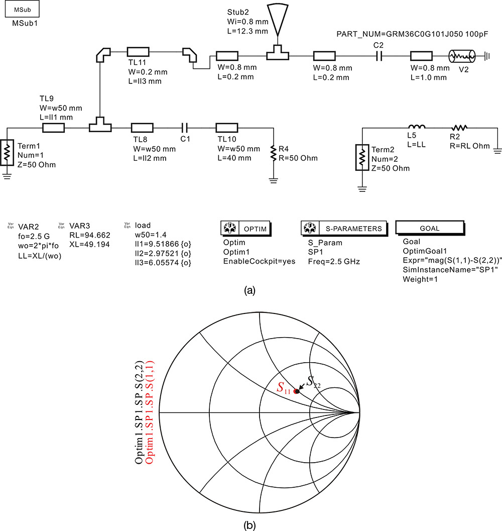
Figure 10.54 (a) Load configured with a microstrip circuit. The optimized values are in the variables of VAR named load. In (a), the line lengths ll1, ll2, and the stub length ll3 are varied. The length ll2 in the simulation is also set to vary taking into consideration the effect of the DC block capacitor C1. (b) The optimization results and S22 is the reference and S11 is optimized to match S22.
A large-signal oscillator simulation is performed using the lx and cy, and the load circuit is implemented with the microstrip lines. The simulation shows an oscillation frequency of 2.439 GHz and an output power of 5.593 dBm. These values are slightly different from those obtained in the circuit simulation in Example 10.13. However, as mentioned previously, this can be due to the difference in harmonic impedances.
10.5.2.2 EM Simulation
The previously implemented microstrip oscillator circuit accurately predicts the behavior of the actual oscillator; however, more accurate values can be determined through EM simulation. Therefore, EM simulation can also further refine the values previously determined in circuit simulation. The procedure is the same as that described in the previous section. In the case of the gate inductor lx, the layout is generated from the previous microstrip circuit using the ADS autolayout utility and l1 in the generated layout is specified as a variable for a newly defined layout component. By entering the layout component in the schematic window, the simulation can be performed in the schematic window similar to that shown in Figure 10.51(a). The value of l1 changes slightly and is found to be l1 = 14.9 mm.
Internal ports in Momentum are used for the simulation of the cy circuit connected to the source terminal. These ports can cause changes in the ports’ locations when the lengths of the transmission lines defined as variables change. There are several techniques for solving the port location changes. In this design, a fixed-length microstrip in a layer that has no function is used to connect the internal ports, thereby eliminating the changes in the locations of the ports due to the length changes. Also note that the accuracy of the ADS internal port is currently not well known. Using Sonnet for the EM simulation is recommended for greater accuracy. A length l2 = 15.5 mm is obtained through the EM simulation.
The lengths of the microstrip lines in the load circuit connected to the drain terminal are also determined in a similar way through optimization in the EM simulation. The computed values are obtained as ll1 = 9.0 mm, ll2 = 3.13 mm, and ll3 = 5.46 mm. The values obtained in the EM simulation can be seen to be significantly different from those obtained in the circuit simulation.
Figure 10.55 is the schematic of the oscillator whose dimensions are tuned through the separate EM simulations described above. The RFCs DCFEED1 and DCFEED2, and the DC block DC_Block1 in Figure 10.55 are used for computational efficiency. Without these RFCs or the DC block, the frequency of the EM simulation should be extended up to the DC, which significantly increases the computation time beyond what is acceptable and it also degrades the accuracy of the computation in the DC. However, it must be noted that these RFCs or the DC block inserted in the circuit have no effect on the computation at the DC. To this end, the frequency range of the layout components, such as lx and the load circuit, is set to 1–10 GHz. The simulation results are shown in Figure 10.56. Figure 10.56(a) shows the oscillation waveform obtained from the EM simulation, while the spectrum of the oscillation output is shown in Figure 10.56(b). The oscillation frequency and output power in Figure 10.56(b) are 2.461 GHz and 6.825 dBm, respectively. The values are close to those in the circuit design.
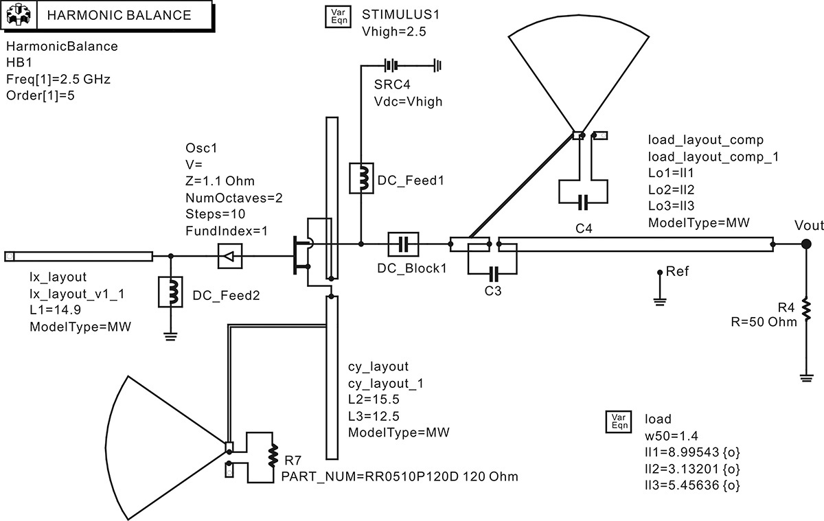
Figure 10.55 Large-signal simulation of a microstrip oscillator circuit using EM simulation. The variables in the layout components are separately determined through the EM simulation and their values are in the schematic. The circuit components such as DC_Feeds and DC_blocks are inserted for fast simulation.
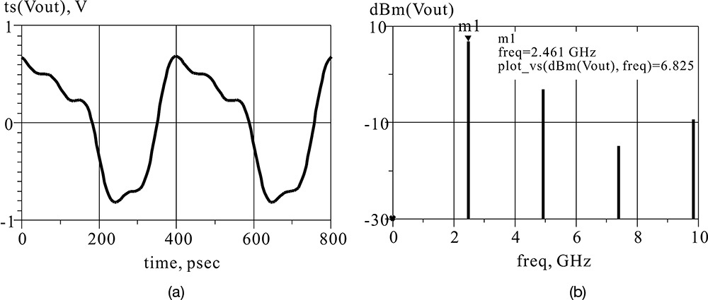
Figure 10.56 (a) Waveform and (b) spectrum from the EM simulation. Oscillation frequency and power are about 2.461 GHz and 6.825 dBm, respectively.
The oscillation frequency can be tuned to the design frequency of 2.5 GHz by varying cy or lx. When lx connected to the gate is varied, the oscillation frequency close to the desired oscillation frequency of 2.5 GHz can be obtained. Figure 10.57 shows the layout of the designed microstrip oscillator.
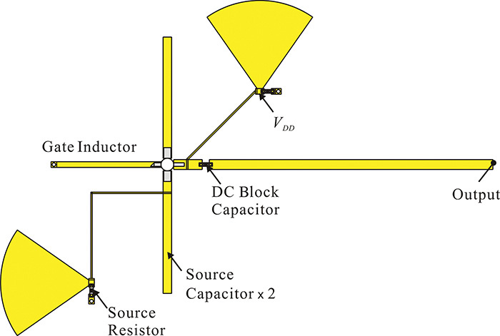
Figure 10.57 Microstrip oscillator circuit layout. VDD represent DC bias supply point. In the layout the coupling between the lines are not considered.
Using independent EM simulations, the layout of the microstrip oscillator shown here is determined by computing the variables of the layout components lx, cy, and the load circuit. This is done to simplify the calculation. Undesired coupling may exist between lx, cy, and the load circuit. The radial stubs of the load circuit and cy circuit in Figure 10.57 are quite close, which requires more accurate calculation. In addition, it can be seen that the bias circuit of the cy circuit and lx circuit are close and this can also cause unwanted coupling. To account for this coupling, the gate, drain, and source terminals of the FET must be set as internal ports, and the EM simulation of the external circuits lx and cy, and the load circuit together should be performed for those defined internal ports. However, since this simulation is not a new process, it can be done by following the previous EM simulation procedure.
10.6 Dielectric Resonators
10.6.1 Operation of Dielectric Resonator (DR)
A dielectric resonator (DR) consists of a dielectric material with a cylindrical form, as shown in Figure 10.58, that has a typical relative permittivity of εr = 30–100 and acts as a resonator due to the high dielectric constant. The dielectric material used for a DR generally has a low loss and the dielectric resonator usually has a Q higher than 103. The size of the dielectric resonator generally expands or shrinks according to temperature change. The size of the dielectric resonator is directly related to its resonant frequency and the temperature change causes the resonant frequency change. The dielectric constant also changes with temperature, which contributes to the change in the resonant frequency as well. Defining the thermal expansion coefficient and temperature coefficient of the dielectric resonator’s dielectric constant as αL and τε, respectively, the temperature drift in the resonant frequency, εf, is expressed in Equation (10.53).
The temperature coefficient of the dielectric constant and the thermal expansion coefficient are dependent on the dielectric material used in the dielectric resonator, and by setting the temperature coefficient of the dielectric constant to compensate for the thermal expansion coefficient, the temperature drift of the dielectric resonator’s resonant frequency can be minimized. As a result of recent studies of dielectric resonator materials, most commercially available dielectric resonators available today are designed to make the resonant frequency’s temperature drift almost zero.
Similar to other resonators, several resonant modes are possible in a dielectric resonator and the fundamental mode with the lowest resonant frequency has the electric field distribution shown in Figure 10.59.
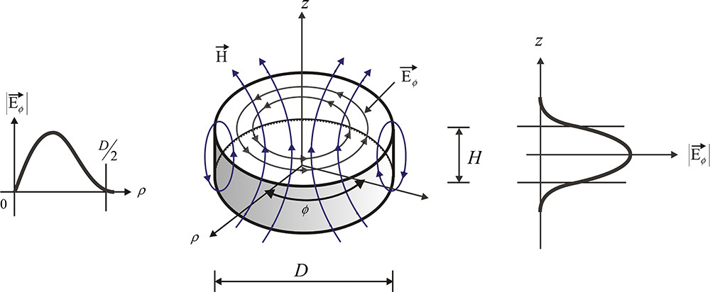
Figure 10.59 The electromagnetic field patterns in a dielectric resonator. The left plot shows the electric field intensity along the ρ-axis. The right plot shows the electric field intensity along the z-axis.
For the cylindrical ρφz coordinate system shown in Figure 10.59, the circumferential electric field appears along the φ-direction and is denoted as Eφ. The distribution of Eφ for the z-axis shows a peak value at z = 0, and it rapidly decays, moving away from z = 0, as shown in the figure. The distribution of Eφ for ρ-axis is 0 at ρ = 0 and it shows a peak value inside the dielectric resonator. The field Eφ also rapidly decays outside of the dielectric resonator. Thus, when the z direction is taken as the propagation direction, the field is said to be in a transverse electric (TE) mode because the electric field exists only in the transverse plane of the propagation direction. The distribution of the electric field Eφ can be represented by a mode number that represents the standing waveform in each axis. The mode number in the ρ-axis is close to 1 and in the φ-axis it is 0 since there is no standing wave. The mode number in the z-axis is represented by δ since a complete standing wave is not established. Thus, the resonant mode in Figure 10.59 is called the TE10δ mode.
On the other hand, the shape of the magnetic field primarily occurs as it passes through the dielectric resonator, as shown in Figure 10.59, which is generated by the time-varying electric field Eφ according to Maxwell’s equations. Note that the electric field inside the dielectric resonator is small and can be approximated as 0 as εr → ∞ according to Maxwell’s equations; otherwise, an infinite magnetic field occurs, which is impractical. Consider the case where the external magnetic field penetrates the dielectric resonator, as shown in Figure 10.59. The electric field Eφ is then generated according to Faraday’s law of electromagnetism. The induced electric field Eφ again generates a magnetic field that occurs in a direction that cancels the incident magnetic field. Since the dielectric resonator is not a magnetic material, its relative permeability can be considered to be 1, and the finite electric field Eφ is induced. Then, the magnetic field generated by the finite-induced electric field Eφ becomes ∞ due to εr → ∞ as the generated magnetic field is proportional to the relative permittivity εr, which is unacceptable. As a result, the magnetic field inside the dielectric resonator is therefore close to 0. Otherwise, a small incident magnetic field can cause an infinite magnetic field in the opposite direction. This phenomenon of the electromagnetic field in the dielectric resonator is similar to that of an eddy current electromagnetically generated in a conductor. Therefore, the magnetic field with z-direction at the surface of the dielectric resonator can be approximated as zero.
The dielectric resonator with the properties previously described is usually coupled to the microstrip shown in Figure 10.60. The microstrip’s magnetic field is incident to the dielectric resonator in the z-direction as shown in that figure and the magnetic field that penetrates the dielectric resonator becomes almost 0 at the resonant frequency of the dielectric resonator. In order to make the magnetic-field lines penetrate the dielectric resonator vertically, the resonator must be positioned higher than the substrate on which the microstrip is placed. To achieve this effectively, a separate spacer is inserted beneath the resonator, as shown in Figure 10.60, which makes the possible magnetic-field lines penetrate the resonator vertically. The magnetic field corresponds to the microstrip current and since the magnetic field at the resonant frequency of the dielectric resonator is 0, the microstrip current will be zero. As a result, the microstrip will be open circuited at the plane where the microstrip is coupled with the dielectric resonator.
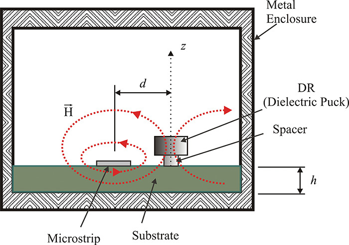
Figure 10.60 Coupling a dielectric resonator to a microstrip. The dielectric resonator is coupled by the magnetic field of the microstrip.
The circuit shown in Figure 10.61(a) represents the dielectric resonator coupled to a microstrip and its equivalent circuit can be represented as shown in Figure 10.61(b). When the distance d in Figure 10.61(a) is small, the coupling between the dielectric resonator and the microstrip becomes tight and the magnetic field of the microstrip is significantly affected by the resonator. On the other hand, when the distance is large, the coupling between the dielectric resonator and the microstrip becomes loose, and the effect of the resonator almost vanishes. Note that the length l in Figure 10.61(a) represents the plane where the microstrip is most tightly coupled to the dielectric resonator and the magnetic field is considered to be 0. Since the magnetic field is 0, the current is also 0 and the microstrip line is thus open circuited at the length l. The circuit in Figure 10.61(a) is represented by the equivalent circuit shown in Figure 10.61(b). Here, the transformer n represents the degree of coupling between the dielectric resonator and the microstrip, which is a function of d and the parallel resonant circuit Lr–Cr–Rr represents the dielectric resonator. The circuit in Figure 10.61(b) can be transformed into the circuit shown in Figure 10.61(c). The impedance seen from the transformer port connected to the microstrip line is a parallel resonant circuit and the circuit in Figure 10.61(c) can then be obtained. It should be noted that the resonance frequency of the circuit in Figure 10.61(c) is the same as that in Figure 10.61(b). However, the values of R, L, and C differ from those of Rr, Lr, and Cr. The value of resistor R reflects the degree of coupling between the dielectric resonator and the microstrip, which is a function of d.
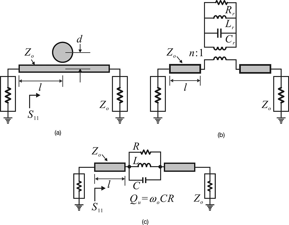
Figure 10.61 (a) Dielectric resonator circuit, (b) equivalent circuit, and (c) simplified equivalent circuit
Setting l = 0 in the circuit of Figure 10.61(c), the locus of S11 with frequency can be plotted as shown in Figure 10.62(a) with d as a parameter. The dielectric resonator has a negligible effect on the microstrip line for frequencies outside the resonant frequency; consequently, the impedance seen from the port is close to Zo = 50 Ω and appears at the origin of the Smith chart. However, the impedance seen from the input port at the resonant frequency becomes Zo + R and this is represented by point A on the Smith chart in Figure 10.62(a). In addition, this point depends on the coupling between the microstrip and the dielectric resonator. When the coupling is very tight, R → ∞, and the impedance appears at a point ∞ of the Smith chart. Therefore, when the coupling is very tight, the impedance seen from the port at the resonant frequency is close to infinity.
Figure 10.62 (a) Frequency response of S11 (l = 0) with respect to the change of d (d3 < d2 < d1) and (b) the tightly coupled S11 (d3) with respect to the change of l
For the tightly coupled dielectric resonator (d3), Figure 10.62(b) shows the change of the S11 locus with the length l as a parameter. The locus rotates in a clockwise direction as l increases. Thus, denoting the electrical length at the resonant frequency as θ(l), the peak reflection coefficient Γin (l) of S11 in Figure 10.62(a) is obtained by rotating ΓA by 2θ(l), as expressed in Equation (10.54).
Note that any reactance jX around the unit circle of the Smith chart can be implemented by varying the length l. In addition, the implemented jX that uses the dielectric resonator only appears near the resonant frequency and rapidly approaches Zo as the frequency slightly away from the resonant frequency. The narrow-band implementation of jX is important in oscillator design. To emphasize its importance, the circuit is redrawn in Figure 10.63(a) where the dielectric resonator is placed at a distance θ away from the port and the S11 locus is shown in Figure 10.63(b). In the circuit configuration of Figure 10.63(a), the impedance seen from the port behaves as the open-circuited transmission line with an electrical length of θ near the resonant frequency, as shown in Figure 10.63(b), and the impedance becomes Zo at other frequencies. Thus, the oscillation condition can be satisfied only at the resonant frequency. At other frequencies, the oscillator circuit is generally stabilized because the impedance seen from the port is close to Zo and the oscillation condition is not satisfied except at the resonant frequency. As a result, the undesired oscillation condition at other frequencies can be easily avoided.
Figure 10.63 (a) A circuit of the DR coupled to microstrip and (b) its S11 locus apart from θ. By varying θ, all the reactance in the Smith chart can be implemented.
10.6.2 Extraction of the Equivalent Circuit of a DR Coupled to a Microstrip
In this section, we look at the method for extracting the values of the equivalent circuit for a dielectric resonator coupled to a microstrip. Denoting the impedance of the parallel resonant circuit in the circuit of Figure 10.61(c) as Zp, S11 is expressed in Equation (10.55),

where
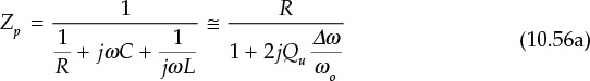
In Equations (10.56a)–(10.56c), Qu is the unloaded Q of the dielectric resonator. Substituting Zp into Equation (10.55) and rewriting it, we obtain Equations (10.57a)–(10.57c).
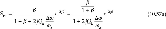
Figure 10.64 shows the plot of |S11| with respect to frequency.
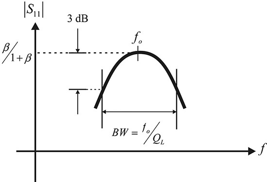
From Equation (10.57a), the peak value of |S11| occurs at the resonant frequency fo. Since the peak value at the resonant frequency is β/(1 + β), β can be obtained from the measured peak value. As a result, the value of R can be obtained using Equation (10.57b). Furthermore, from the measured 3-dB bandwidth in Figure 10.64, the loaded Q, QL, can be found as expressed in Equation (10.58).
Thus, Qu, the unloaded Q, can be determined by substituting β and QL into Equation (10.57c). From the computed Qu, the value of C can be determined using Equation (10.56c). Finally, the value of L can be obtained from the resonant frequency fo and C using Equation (10.56b). Therefore, all the component values of the equivalent circuit can be determined using the frequency response of |S11|.
Figure 10E.29 shows the frequency response of |S11| for a dielectric resonator coupled to a microstrip. In that figure, fo = 10 GHz, |S11|max = -7.06 dB, and BW = 90 MHz. Calculate the values of the microstrip circuit’s equivalent circuit that is coupled to the dielectric resonator in Figure 10.61(c).
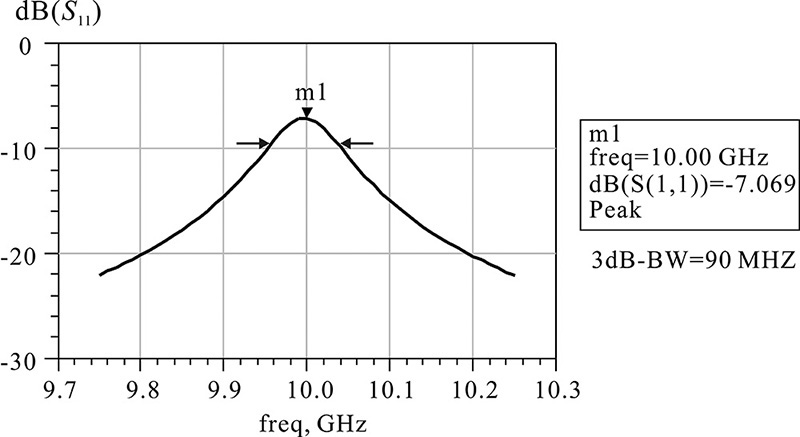
Figure 10E.29 Frequency response example of the dielectric resonator coupled to the microstrip circuit
Solution
From |S11|max = -7.06 dB, β can be obtained as
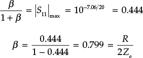
From β, the value of R can be obtained as
R = 800Ω
From BW = 90 MHz and resonant frequency fo = 10 GHz, QL and Qu can be obtained as
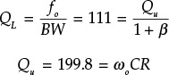
Thus,
The value of L is also obtained from ωo as
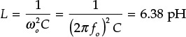
Therefore, the values of the components in the equivalent circuit that yield the given frequency response are as follows:
R = 80Ω, C = 39.73 pF, L = 6.38 pH
In Example 10.14, the equivalent circuit of the dielectric resonator coupled to microstrip is extracted using its S-parameters. The S-parameters can be obtained by measurement or from the 3D-simulation of the dielectric resonator coupled to a microstrip. The programs developed by vendors of dielectric resonators can also be used to compute the values of the equivalent circuit in Example 10.14.9
9. One of these programs can be found on the website for Trans-Tech, www.trans-techinc.com.
10.7 Dielectric Resonator Oscillators (DRO)
We saw in the preceding sections that a microstrip oscillator can be designed by replacing the capacitors and inductors of the basic series feedback oscillator by open- or short-circuited microstrip lines. There are several ways of designing a DRO (dielectric resonator oscillator) but the simplest method is to replace one of the capacitors and one of the inductors with a dielectric resonator coupled to a microstrip circuit as previously described. Another method is to use the dielectric resonator as a feedback resonator circuit. This section will discuss these two design methods.
In addition, we will present an oscillator design that meets the given phase noise design objective. The phase noise generation in an oscillator is basically a nonlinear phenomenon. The near carrier phase noise is primarily generated as a result of a nonlinear conversion of the low-frequency noise sources in an oscillator’s components. This has been confirmed by significant recent research; see reference 3 at the end of this chapter for more information. However, the design of a low-phase noise oscillator to meet a given phase noise specification is still theoretical despite current research and the emergence of modern CAD simulators. In addition, the low-frequency noise models of active devices for phase noise simulation are not available for most CAD simulators and they should be prepared by designers. Rather than the design that uses phase noise simulation, we will present an experimental design method that meets the phase noise design’s objective based on Leeson’s formula. The measured phase noise of the prototype oscillator makes it possible to estimate the Q of the resonator which meets the phase noise design objective using Leeson’s formula. In this section, we will show that the desired phase noise can be achieved through the reconfiguration of the resonator to yield the estimated Q.
10.7.1 DRO Design Based on Replacement
In Example 10.13, we showed how to compute the feedback circuit element values x, y, and ZL. The circuit at which the dielectric resonator is coupled to a microstrip, shown in Figure 10.63, can be used to replace x or y in the feedback circuit elements, which enables us to build the DRO. This type of DRO is called a reflection-type DRO.
Using the feedback circuit element values x, y, and ZL obtained in Example 10.13, design a 2.5-GHz DRO. The dielectric resonator coupled to a microstrip circuit (DR circuit) has Qu = 3000 and QL = 40.
Solution
In Example 10.13, the values of x and y can be implemented by an inductor and a capacitor, respectively. Note that the gate should be grounded at the DC. When x is implemented using the DR circuit, the gate terminal is connected to the ground through the 50-Ω resistor. Since the gate current is 0, the gate voltage is still 0 and the same self-bias circuit can be used without change. In contrast, when y is implemented by the DR circuit, a DC block capacitor is necessary so as not to disturb the self-bias circuit set by the source resistor RS. In addition, since y should be implemented using two parallel connections, it is difficult to implement y using the DR circuit. Thus, the replacement of x by the DR circuit is the preferred method.
Figure 10E.30 is the simulation schematic for determining the length θ in Figure 10.63.
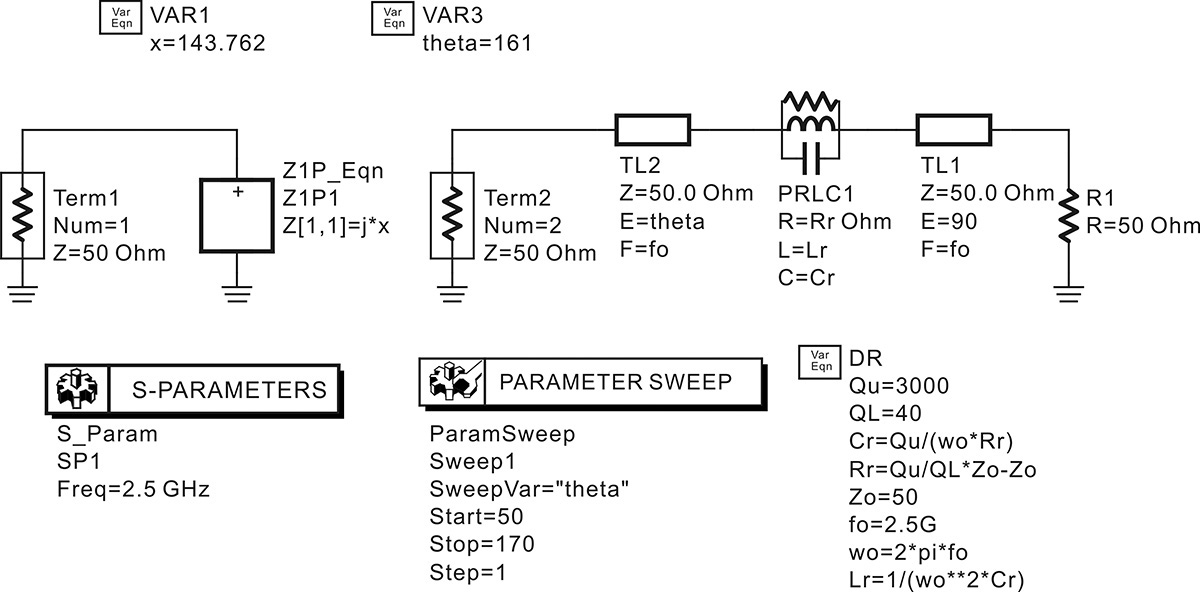
First, using the given Qu and QL, the values of R, L, and C can be computed using
These equations are included in a VAR named DR. The x is implemented using the equation component in ADS shown at the left of Figure 10E.30. The length q can be found by sweeping theta, which gives the same value of x. Figure 10E.31 shows S11 and S22. From that figure, the value of theta that gives the value of x is 161°. Now, replacing lx by the DR circuit in Figure 10E.30, the simulation can be performed. The simulated voltage waveform and spectral power are shown in Figures 10E.32(a) and (b), respectively. The oscillation frequency and power are 2.499 GHz and about 2.9 dBm, respectively. Although the oscillation close to 2.5 GHz is achieved, the oscillation power is significantly reduced from 6.3 dBm.
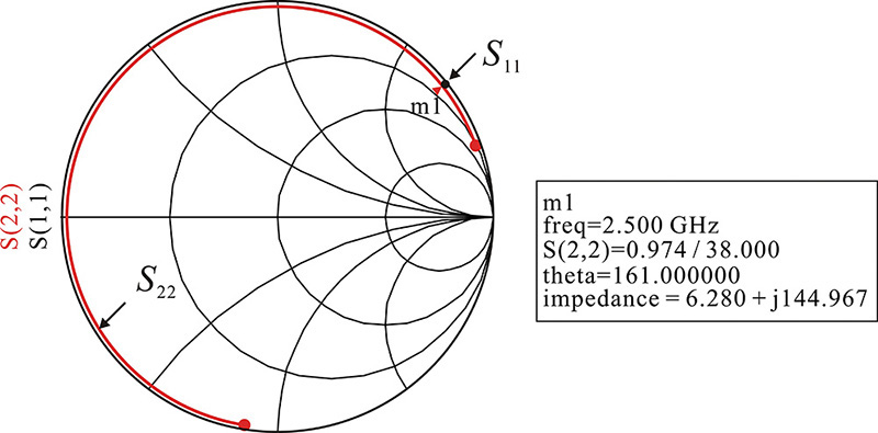

Figure 10E.32 (a) Simulated waveform and (b) spectral power of the DRO that is implemented by replacing x with the DR-coupled microstrip circuit
The reason for the reduced oscillation power is due to the loss of the DR circuit. This circuit cannot be considered as pure reactance but one that has loss. The loss can be found from the S-parameter shown in Figure 10E.31. The real part of the DR circuit is 6.28 Ω.
The disadvantage of this DRO design is that it may not take full advantage of the high Q of the dielectric resonator. Note that the loss of the dielectric resonator coupled to the microstrip circuit is small for a large value of β according to Equation (10.57a). This large value of β lowers the value of QL in Equation (10.57c). Consequently, the phase noise performance of the DRO that is related to QL is diminished. Thus, the design that takes advantage of the high Q of a dielectric resonator requires that the loss of the DR circuit be taken into account.
10.7.2 Dielectric Resonator Oscillator Design Using Feedback
10.7.2.1 Design Theory
An alternate way to design a DRO is to use the closed-loop configuration shown in Figure 10.65.10 The dielectric resonator is used in the resonator shown in that figure. Here, the amplifier provides a sufficient loop gain, the oscillation frequency is adjusted using the phase shifter, and the output power is obtained by coupling a part of the oscillation power in the loop.
10. B. I. Son, H. C. Jeong, and K. W. Yeom, “Design of a Low Phase Noise Voltage Tuned DRO Based on Improved Dielectric Resonator Coupling Structure,” Asia-Pacific Microwave Conference Proceedings, Kaohsiung, Taiwan (December 4–7, 2012): 1121–1123.
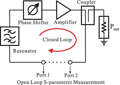
The open-loop gain L(ω) given by Equation (10.18) can be obtained from the open-loop S-parameters of the cascade chains of the resonator, the phase shifter, and the amplifier. Usually, each component in Figure 10.65 is designed to have a small reflection in order to avoid a mismatch between the components. Thus, S11 and S22 of the open-loop S-parameters can be assumed to be small. In addition, the reverse gain S12 is small due to the amplifier’s properties. Assuming S11, S22, and S12 are small, Equation (10.59) can be derived.
From Equation (10.59), the oscillation condition can be rewritten as Equations (10.60a) and (10.60b).
To design an oscillator based on the open-loop gain method, the S-parameters for the open loop are measured. Then, when Equations (10.60a) and (10.60b) are satisfied at a desired oscillation frequency, the oscillator can simply be formed by closing the open loop.
From a design point of view, the phase shifter, amplifier, and resonator are independently designed in advance and the designed components are connected in cascade to form the oscillator. Denoting the S-parameters of the phase shifter, amplifier, and resonator as Sϕ, SA, and SR, respectively, the open-loop gain S21 can be expressed as Equation (10.61).
Therefore, in order to satisfy the oscillation conditions given by Equation (10.60), |S21| has to be set greater than 1 and the phase of S21 should satisfy Equation (10.62).
Typically, the sum of the phases does not satisfy Equation (10.62). In this case, the oscillator can be designed by adding a 50-Ω transmission line with the appropriate electrical length to satisfy Equation (10.62). In addition, the group delay of the open-loop gain can be obtained by differentiating Equation (10.62) with respect to frequency, and the group delay of the open-loop gain becomes the sum of each component’s group delays. However, as the group delay of the resonator is dominant, the group delay is determined by that of the resonator. Thus, the resonator must be designed to have the group delay that satisfies the design goal of the oscillator. This method is useful and efficient not only for theoretical design but also for the experimental design of an oscillator.
The oscillation frequency can be tuned using the phase shifter. The oscillation frequency occurs where the phase of S21 is 0 and the zero of the phase S21 changes by the phase shifter. Typically, the amplifier and phase shifter in Figure 10.65 have broadband characteristics and only the resonator has narrowband characteristics. Thus, the frequency response of the open-loop gain appears similar to that of the resonator, as shown in Figure 10.66. Given that a phase shifter has a maximum phase shift of ±Δθ, the phase shift of ±Δθ is found to correspond to frequencies f1 and f2 from Figure 10.66. Thus, an electrical frequency tuning range of Δf = f2 - f1 is obtained by tuning the phase shifter. The slope of the phase of the open-loop gain at the center frequency fo becomes the group delay and is defined by
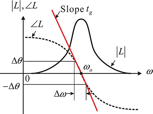
Figure 10.66 The frequency response of the open-loop gain. The dotted line represents the phase and solid line represents the magnitude of the open-loop gain. The slope of the phase at the center frequency is the group delay.
Using Equation (10.63), the electrical frequency tuning range Δf becomes Equation (10.64).
Here, Δθ is expressed in degrees. Thus, the higher the group delay, the narrower the electrical frequency tuning range becomes.
However, the Leeson’s formula for the phase noise S(fm) is rewritten as Equation (10.65).
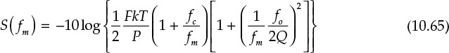
Here, fm and fc represent the offset and flicker frequencies, and P and F represent the oscillation output power and noise figure of the amplifier, respectively. The Q in Equation (10.65) becomes the QL of the open loop gain, and QL is expressed in terms of the group delay as Equation (10.66).
Therefore, the phase noise is improved as the group delay increases and this improvement is quite obvious from Equation (10.65).
Suppose that a phase noise of S1 (dBc/Hz) is obtained when the oscillator shown in Figure 10.65 is formed with a group delay of tg1. Assume that the group delay of the resonator is improved to a larger value tg2, but other oscillator components remain the same. Then, the electrical frequency tuning range that results will be reduced by tg2/tg1, while the phase noise of the newly designed oscillator S2 (dBc/Hz) will be improved, as expressed in Equation (10.67).
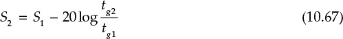
Thus, the phase noise can be systematically improved using the open-loop method. In conclusion, from Equations (10.64) and (10.65), the electrical frequency tuning range and the phase noise are found to have a trade-off relationship and the group delay of the open-loop gain is found to be a key parameter of that trade-off relationship.
In the derivation of Equation (10.67), we assumed that fc, P, and F are invariant for the resonator change. However, the two values of F and fc in Equation (10.65) for the resonator change may not be exactly equal. Although the identical insertion loss is assumed for the two resonators, the harmonics of the two DROs differ and this results in different noise conversions. However, assuming that the harmonic signals are small and ignoring the harmonic contributions in the noise conversion, the two values of F and fc in Equation (10.65) can be approximated to be equal.
10.7.2.2 DRO Components
An amplifier layout for the HMC313 from Hittite is shown in Figure 10.67.11 The schematic shown in Figure 10.67(a) is the recommended circuit in the datasheet and Figure 10.67(b) shows the layout. The points marked with • in Figure 10.67(b) represent the wafer-probe contact pads that enable two-port S-parameter measurement using on-wafer probing. All the chip DC block capacitors in Figure 10.67(b) have a value of 100 nF and the bypass capacitor CT2 is a 0.33-uF-chip tantal capacitor.12 From the datasheet, the magnitude and phase of S21 are 17 dB and -75°, respectively, for a DC bias of 5 V and DC current of 47 mA.
11. Hittite, HMC313, GaAs InGaP HBT MMIC amplifier, available at www.hittite.com.
12. American Technical Ceramics, ATC 500S, ATC 545L capacitor, available at www.atceramics.com.
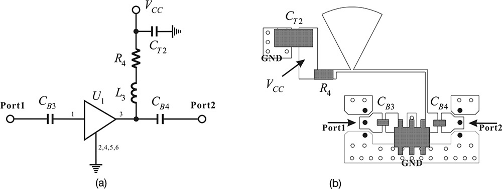
Figure 10.67 (a) Amplifier schematic where U1 = HMC323, R4 = 0, CT3 = 0.33 μF, L3 is a one-quarter-wavelength choke, and CB3 and CB4 are 100-nF high-frequency DC block capacitors; (b) amplifier layout.
Figure 10.68 shows the measured results and datasheet values of S21. The measured results can be seen to have a gain of 16.1 dB and a phase of approximately 52.5° within the frequency band of interest. The measured gain, S21, is close to the value from the datasheet, but the phase is found to show a significant difference. The phase difference is due to the effects of the 50-Ω microstrip line lengths inserted for mounting the DC block capacitors and the HMC313. However, it can be seen that the gain of the amplifier is sufficiently high to compensate for the insertion losses of the resonator, phase shifter, and output coupler.

Figure 10.68 Comparison of the measured amplifier gain with that given in the datasheet for the HMC313. The dotted line is also from the datasheet. The two gains are close but a significant difference appears in the phase.
Figure 10.69(a) shows the phase shifter circuit.13 In that figure, L1 and L2 are implemented using the identical varactor diodes, the SMV1245 from Skyworks, Inc.14 This diode is series resonant due to packaging inductance and the series resonant frequency is approximately 1.5 GHz. Therefore, when used near the oscillation frequency of 5.3 GHz, the varactor diode acts as a variable inductor. The two varactor diodes are biased by resistors R1, R2, and R3. The reason for using these resistors in the DC bias is that they can remove the parasitic resonance phenomenon that occurs when using an RF choke. Capacitors CB1 and CB2 are 100-nF high-frequency DC block capacitors. Thus, when the DC block and the DC bias resistor are removed, this circuit becomes a traditional all-pass filter and the capacitors C1 and C2 can be determined from Equations (10.68a) and (10.68b).
13. L. Chen, R. Forse, A. H. Cardona, T. C. Watson, and R. York, “Compact Analog Phase Shifters Using Thin-Film (Ba,Sr) TiO3 Varactors,” IEEE MTT-S International Microwave Symposium, Honolulu, HI, (June 3–8, 2007): 67–670.
14. Skyworks, SMV1245-011 varactor diode, available at: www.skyworksinc.com.
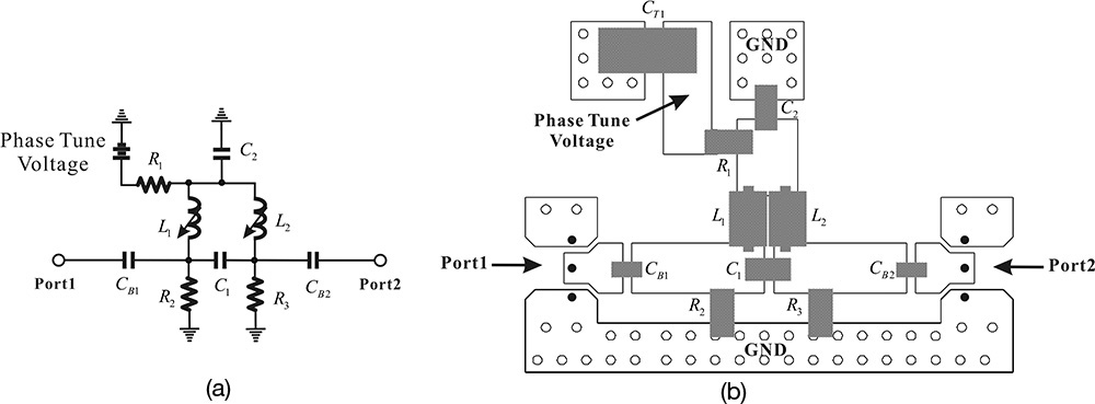
Figure 10.69 (a) Phase shifter circuit: L1 and L2 are varactor diodes, resistor R1 = R2 = R3 = 1 kΩ, capacitor values are C1 = 0.3 pF, C2 = 0.4 pF, CT1 = 0.33 μF, and CB1 and CB2 are high-frequency 100-nF DC block capacitors; (b) phase shifter layout.
Here, ωo and Zo represent the oscillation frequency and 50 Ω, respectively.
The computed values of C1 and C2 are approximately 0.3 pF and 1.2 pF, respectively, and based on these values, the capacitor values can be tuned in ADS simulation to achieve a phase shift of 70°. The value of C2 is adjusted to 0.4 pF, while the value of C1 is similar to the computed value 0.3 pF. Figure 10.69(b) shows the layout of the phase shifter circuit. Wafer-probe pads are inserted in the phase shifter layout to enable the independent S-parameter measurement of the phase shifter as in the case of the amplifier. The wafer-probe pads are shown as • in Figure 10.69(b). The phase shift is measured to be about 72° with respect to the varactor diode tuning voltage. The varactor diode tuning voltage varies between 0–10 V. The return loss varies according to the varactor diode DC tuning voltages. All the return losses are below 10 dB within the oscillation frequency band, which does not cause a serious mismatch in a cascade connection to other components.
10.7.2.3 Prototype Resonator
Figure 10.70 shows a resonator configured using a dielectric resonator, which is Murata’s DRD107UC048.15 At the frequency of 7 GHz, the resonator has parameters such as εr = 37.7 and Qu = 6800. The resonant frequency of the dielectric resonator with a metal-box enclosure can be adjusted from 4.96 to 5.40 GHz. The substrate is RO4350, which has a permittivity of εr = 3.66 and a thickness H = 30 mil.16 The spacer in Figure 10.70 is composed of a ceramic material and has a thickness of 1.016 mm and a relative permittivity of εr = 4.5. The resonance frequency can be adjusted within a frequency range of 100 MHz using the tuning screw that is fixed on the ceiling of the metal-box enclosure. The structure shown in Figure 10.70 is analyzed using Ansoft’s HFSS to obtain the desired resonant frequency of 5.3 GHz by adjusting the tuning screw.17 The detailed dimensions that yield the resonant frequency of 5.3 GHz are shown in the caption of Figure 10.70.
15. Murata, DRD107UC048 dielectric resonator available at: www.murata.com.
16. Rogers Corp. RO4000R series high-frequency circuit materials available at: www.rogerscorp.com.
17. SpragueGoodman, GRRB70504SN10 dielectric resonator tuners available at: www.spraguegoodman.com.
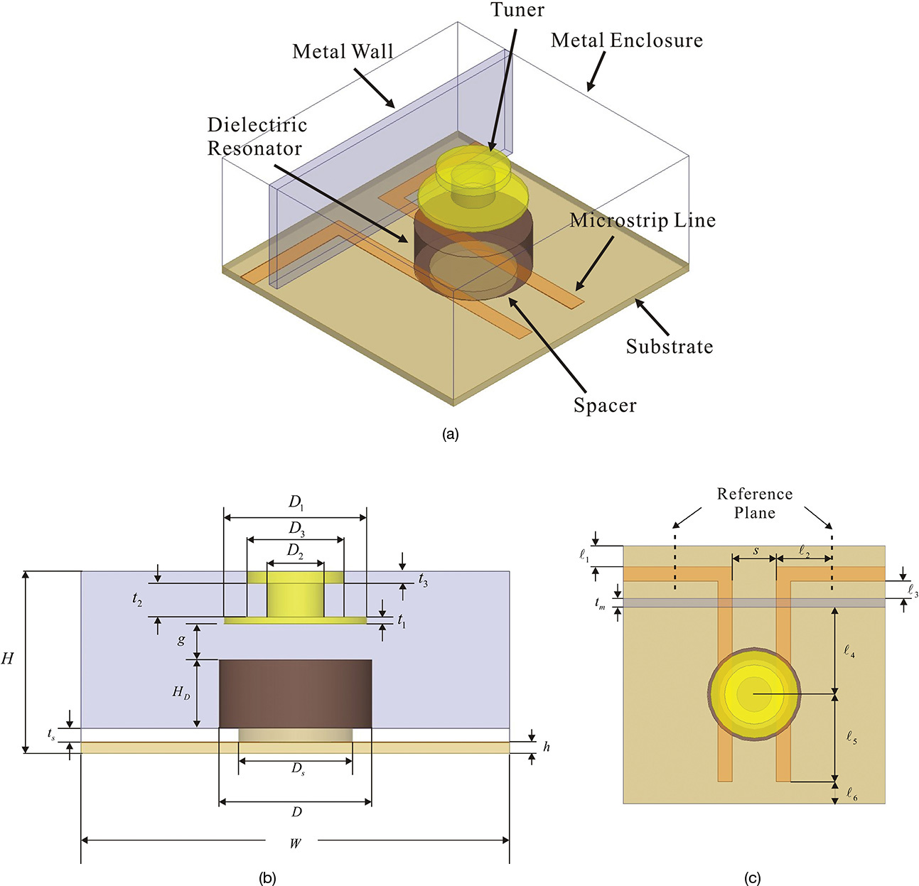
Figure 10.70 (a) Resonator structure; (b) front view dimensions: W = 30, H = 12.762, h = 0.762, Ds = 8.001, ts = 1.016, D = 10.75, HD = 4.77, g = 2.514, t1 = 0.5, t2 = 2.35, t3 = 0.85, D1 = 10, D2 = 4, D3 = 6.8; and (c) top view dimensions: l1 = 2.36, l2 = 6.5, l3 = 2.0, l4 = 10.0, l6 = 2.5, d = 5.6, w = 1.64 (all units are in mm).
The designed resonator is fabricated and measured. The measured group delay can be derived using the slope of the phase against frequency and the value is measured to be 2.3 nsec as in the simulation. Using the group delay, QL can be computed from Equation (10.64) and the value is calculated to be 38.3. In addition, the electrical frequency tuning of about 84.5 MHz is estimated from Equation (10.62) when the phase shifter with a phase shift of ± 35° is employed in the oscillator.
10.7.2.4 Prototype DRO
Figure 10.71 shows the layout of the prototype oscillator that includes each of the separately designed and measured components. It can be seen from Figure 10.71 that the layout is designed to allow the independent S-parameter measurement of each block such as the resonator, amplifier, and phase shifter using a wafer probe. After measurement is carried out for each component, the components are connected in cascade by soldering 0-Ω resistors for R5, R7, R8, and R9 in Figure 10.71. Using this method, a closed-loop oscillator can be formed. The 50-Ω microstrip lines l1 and l2 in Figure 10.71 are deliberately inserted to make the phase of the open-loop gain to be an integer multiple of 360° at the oscillation frequency of 5.3 GHz. The oscillation output is obtained through capacitor C3. After disconnecting one of the resistors R5, R7, R8, or R9 in Figure 10.71, the open-loop gain can be measured using wafer probes by placing those probes on the disconnected wafer-probe pads. In the open-loop gain measurement, a 50-Ω coaxial termination is connected to the oscillation output terminal.
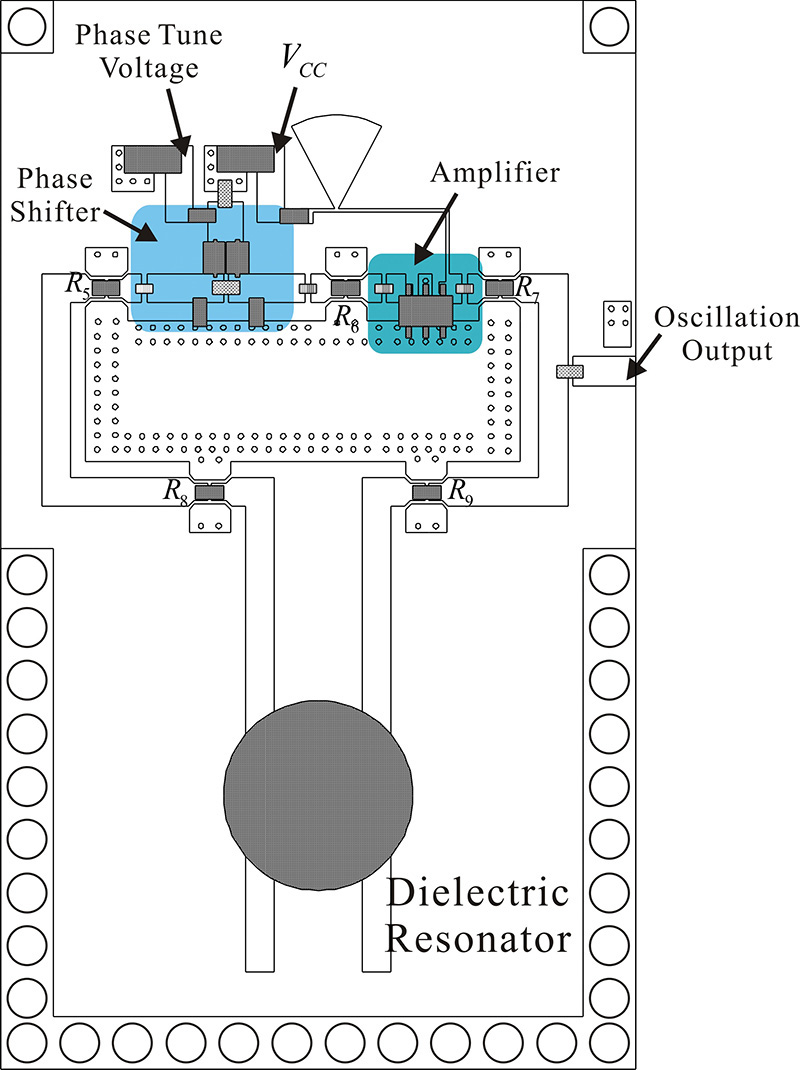
Figure 10.71 The prototype dielectric resonator oscillator layout (44 × 72 mm2). Resistors R5, R6, R7, R8, and R9 are 0-Ω resistors for connection.
Figure 10.72 shows the measured open-loop gain using an Agilent E8358A network analyzer. The phase tune voltage is set to 6 V, which corresponds to about the center value of the DC phase tune voltage range, which also corresponds to about the center frequency of the oscillator. The magnitude of the open-loop gain, S21, is greater than 0 dB at the center frequency of 5.3 GHz, and the phase can be seen to be 0° at a frequency of 5.313 GHz. Therefore, the oscillation frequency can be expected to occur at 5.313 GHz, which is close to 5.3 GHz. The group delay can be obtained by calculating the slope at the frequency where the phase is 0°. Thus, the group delay is
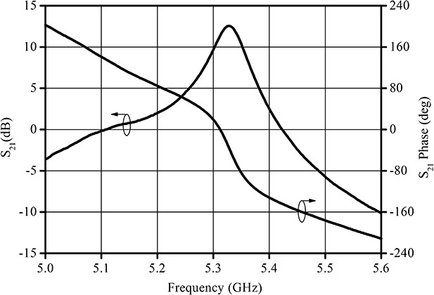
Figure 10.72 The measured open-loop gain (the DC phase tune voltage of the phase shifter is set to 6 V).
The characteristics of the DRO can be measured with a spectrum analyzer; however, for more precise measurements, an Agilent E5052A signal source analyzer is used for the measurement. The electrical frequency tuning range is measured to be 99 MHz (5.264–5.363 GHz) at the phase tune voltage change of 0–10 V. The electrical frequency tuning range can be computed from the group delay, which is obtained from the open-loop gain measurement. From Equation (10.62), the electrical frequency tuning range is calculated to be
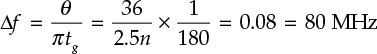
Note that the electrical frequency tuning characteristic appears to be the same as the phase shifter’s phase tune characteristic from Equation (10.62). Thus, the closer that phase tune characteristic is to a straight line, the more linear the electrical frequency tuning characteristic appears to be. Therefore, in order to have a linear frequency tuning characteristic, a phase shifter with a linear phase tune characteristic is required.
Figure 10.73 shows the phase noise characteristics measured with the E5052A signal analyzer from Agilent Technologies.18 Figure 10.73(a) shows the phase noise characteristic at the center frequency of 5.3 GHz when the phase tune voltage is about 6 V. In that figure, the phase noise is about -111 dBc/Hz at the offset frequency of 100 kHz. Figure 10.73(b) shows the phase noise when the phase tune voltage is varied with the offset frequency fixed to 100 kHz. From the figure, even though the oscillation frequency is changed, the phase noise remains constant. Note that when the phase tune voltage is changed, the phase of the open-loop gain changes; however, the group delay does not change because it is chiefly determined by the resonator. As a result, regardless of the change in the phase tune voltage, a constant phase noise is displayed due to an approximately constant group delay. Usually, when the resonant frequency of the resonator is tuned using a frequency tuning device, such as a varactor diode, the Q of the resonator varies according to the resonant frequency change. Therefore, when the resonant frequency of the resonator is directly tuned using a frequency tuning device, the phase noise varies according to the variation in the oscillation frequency. However, when the oscillation frequency is tuned using a phase shifter, the Q of the resonator does not change and a constant phase noise is obtained regardless of the oscillation frequency tuning.
18. Agilent Technologies, 5989-6389EN, Agilent E5052B signal source analyzer, 10 MHz to 7, 26.5, or 110 GHz, 2007 available at: www.agilent.com.
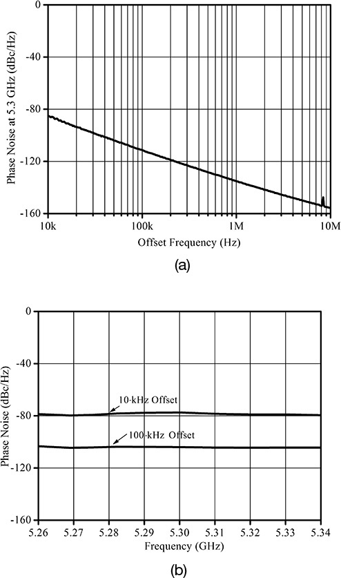
Figure 10.73 Frequency tuning characteristics of the fabricated DRO: (a) phase noise characteristics at an oscillation frequency of 5.3 GHz, and (b) phase noise at an offset frequency of 10 kHz and 100 kHz when the phase tune voltage is varied
10.7.2.5 Low Phase Noise DRO
There are often many applications that require further improvement in phase noise rather than in the wide electrical frequency tuning range. Suppose that the basic configuration of the oscillator is unchanged. Then, from Equations (10.63) and (10.64), it can be found that the increase in group delay leads to a narrower electrical frequency tuning range and improved phase noise. The improvement in phase noise due to an increased group delay can be estimated using Equation (10.67). Thus, when the design objective is set to a phase noise of -130 dBc/Hz at a 100-kHz offset frequency, the group delay of a resonator with more than 50 nsec (approximately 20 times improvement in the group delay of the previous DRO) is based on Equation (10.67).
Figure 10.74 shows a resonator configured with a dielectric resonator identical to that shown in Figure 10.70. The group delay of the resonator primarily depends on the distance (D) between the microstrip and the center of the resonator, and the length extension (L) of the microstrip from the center of the dielectric resonator, as shown in Figure 10.74. The width of the microstrip line can also be a variable but the width is fixed to that of the 50-Ω microstrip shown in Figure 10.70.

Figure 10.75(a) shows the change of group delay with respect to D and L. The group delay of Figure 10.75(a) is related to the coupling between the dielectric resonator and the microstrip. Note that the coupling between them is magnetic. For a strong magnetic-field incident on the dielectric resonator from the microstrip, the coupling is high, while it is low for a weak magnetic-field incident. As D increases, the magnetic-field incident becomes weaker and the coupling becomes low. Note that the high coupling of the microstrip makes the loaded Q, QL decrease from the Qu of the dielectric resonator. Thus, QL increases as the coupling becomes lower, thereby increasing group delay because QL = πfotg. As a result, the group delay increases with the increase of D. The group delay variation with respect to L can be understood from the current standing wave pattern. Since the end of the microstrip line is open, the current is a maximum at point P when point P is placed away from the microstrip end by a quarter wavelength (L = 7.4 mm). Thus, the coupling by the microstrip’s magnetic field is maximum and the group delay is minimum at L = 7.4 mm. The group delay increases when L increases or decreases from a quarter wavelength because the current corresponding to the magnetic field at point P decreases when L is away from a quarter wavelength. Consequently, the group delay increases with the increase of D and is lowest near L = 7 mm, as shown in Figure 10.75(a).
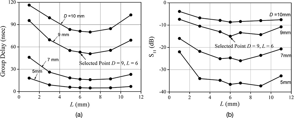
Figure 10.75 Simulation results of a resonator: (a) group delay and (b) return loss. The results are computed using AnSoft’s HFSS.
In the DRO design, since the return loss and insertion loss depend on D and L, not only the group delay but also the return loss and the insertion loss should be considered simultaneously. A high insertion loss requires a high-gain amplifier. In that case, an amplifier with an impractically high gain is required to cause oscillation even though the group delay is high. In addition, when the return loss is small, the open-loop gain cannot simply be expressed as S21 due to the mismatch between other components such as the phase-shifter and the amplifier. As a result, the mismatch must be taken into account in the design process, which in turn makes the design difficult.
Figure 10.75(b) shows the variation of |S11| that is similar to the variation of the group delay in Figure 10.75(a). As D increases, a smaller power from the microstrip is delivered to the dielectric resonator. Thus, most of the power is not delivered to the other port but rather is reflected. This makes |S11| high as D increases. Since |S11| is high, the insertion loss increases. Therefore, the increased group delay necessarily accompanies both a larger insertion loss and smaller return loss. The distance D = 9 mm and the length L = 6 mm are chosen. The resulting group delay is 53 nsec, dB(S11) < -10 dB, and dB(S21) = -2 dB. Using Equation (10.65), the expected phase noise for the determined D and L is -132 dBc/Hz, and the electrical frequency tuning range is calculated to be 5 MHz. Compared to the previous DRO design, the phase noise at an offset frequency of 100 kHz is computed to be improved by approximately 26 dB and the frequency tuning range is reduced by about 1/20.
Figure 10.76 is a photograph of the DRO with the newly designed resonator. In this photograph, only the resonator has been changed and the remaining parts are basically the same as in the previous DRO circuit.
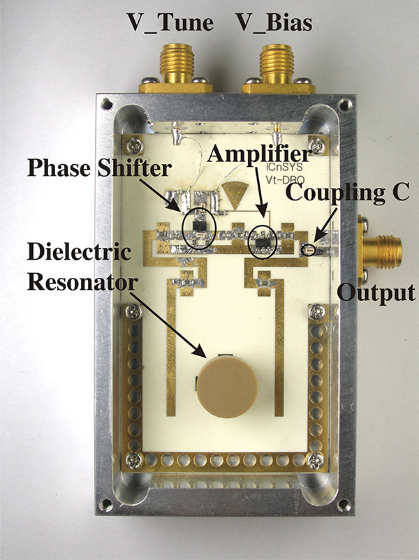
Figure 10.77 shows the measured results for the newly designed DRO using Agilent’s E5052A signal analyzer. The measured electrical frequency tuning range is found to be approximately 5 MHz at a phase tune voltage of 0–10 V. An output power of approximately 4.5 dBm is measured at a phase tune voltage of 6 V. The phase noise against the frequency offset is shown in Figure 10.77 and the phase noise at a frequency offset of 100 kHz is measured to be -132.7 dBc/Hz. This result can be seen to be close to the phase noise predicted using the group delay. Similar to the prototype DRO, the phase noise with respect to oscillation frequency at a constant frequency offset is observed to be almost flat. This is the advantage of the loop-type DRO where the oscillation frequency is controlled using the phase shifter.
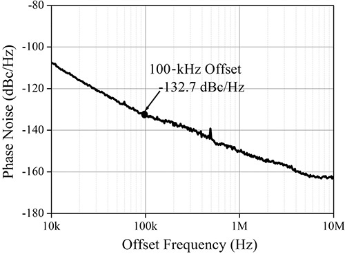
Figure 10.77 Measured phase noise of the fabricated low phase noise DRO employing the improved resonator at a phase tuning voltage of 6 V
10.7.3 Comparison between the Two DRO Design Methods
We have so far investigated two design methods. One design is for a DRO that uses a dielectric resonator in the feedback network of the oscillator; the other design is the reflection-type method (discussed in section 10.7.1) that replaces the reactance x or y with a dielectric resonator coupled to a microstrip circuit. In terms of phase noise, one does not have an advantage over the other. From the design point of view, the phase noise of the reflection type may not be systematically improved and this type also does not provide a systematic way to tune an oscillation frequency. On the other hand, the feedback type is easy to design and its phase noise and electrical frequency tuning range can be systematically improved.
10.8 Summary
• Whether or not a circuit oscillates can be checked using the small-signal oscillation conditions. Oscillation conditions can be described using impedances, reflection coefficients, and open-loop gain; however, they all give the same results for oscillation start-up.
• The oscillation power and frequency can be determined using the large-signal oscillation condition or the equilibrium conditions described using large-signal impedances, reflection coefficients, or open-loop gain.
• The amplitude and phase of an oscillation waveform fluctuates with time. The amplitude fluctuation is specified using AM noise and that of the phase is specified using phase noise.
• The phase noise spectrum can be determined using the ratio of noise to carrier power measured at a given frequency offset. The spectrum analyzer or other devices such as a signal analyzer or specially built equipment can be used to measure the phase noise.
• Phase noise is basically a nonlinear phenomenon; however, phase noise can be empirically described by Leeson’s phase noise model. The near carrier phase noise is primarily dependent on the flicker noise of an active device in an oscillator.
• The simplified oscillator circuits at the RF are generally converted into two types of basic oscillator circuits: the series-feedback- and the parallel-feedback-type of oscillators. An oscillator circuit can be designed by modifying the basic oscillator circuits and adding DC bias circuits.
• An oscillator circuit yielding the desired oscillation frequency can be designed using the oscillation conditions. The design of an oscillator circuit for mobile communication is demonstrated as an example.
• The design of a microstrip oscillator circuit that provides optimum output power and the desired oscillation frequency is demonstrated. The microstrip oscillator that provides optimum power is designed using the synthesis of the feedback network derived from the load-pull simulation results.
• The operation of a dielectric resonator is introduced. In addition, the extraction of the equivalent circuit for the dielectric resonator coupled to a microstrip line is explained.
• The design of a DRO that meets the phase noise objective is demonstrated. First, the prototype DRO is designed and its phase noise performance is evaluated. Then, from the evaluated phase noise, the Q of the resonator in the DRO can be determined. Once the resonator is determined, the desired phase noise can be achieved.
References
1. G. D.Vendelin, A. M. Pavio, and U. L. Rohde, Microwave Circuit Design Using Linear and Nonlinear Techniques, New York: John Wiley & Sons, Inc., 1990.
2. W. P. Robins, Phase Noise in Signal Sources, London: IEEE Press, 1984.
3. A. K. Poddar, U. L. Rhode, and A. M. Apte, “How Low Can They Go? Oscillator Phase Noise Model, Theoretical, Experimental Validation, and Phase Noise Measurements,” IEEE Microwave Magazine, vol. 14, no. 6, pp. 50–72, September–October 2013.
4. D. Kajfez and P. Guillon, Dielectric Resonators, Dedham, MA: Artech House, Inc., 1986.
5. U. L. Rhode, A. K. Poddar, and G. Bock, The Design of Modern Microwave Oscillators for Wireless Applications: Theory and Optimization, New York: John Wiley & Sons, Inc., 2005.
Problems
10.1 Using the circuit shown in Figure 10P.1 and given that the oscillation equilibrium conditions are satisfied at the reference plane A–A’, prove that the oscillation equilibrium conditions are satisfied even when the reference plane is changed to B–B’. In other words, demonstrate that the oscillation equilibrium is established everywhere in the circuit regardless of the reference plane.
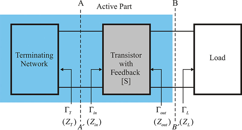
Figure 10P.1 The circuit for Problem 10.1
10.2 Using the circuit shown in Figure 10P.2, determine S11 in a polar format for the circuit at a frequency of 10 GHz.
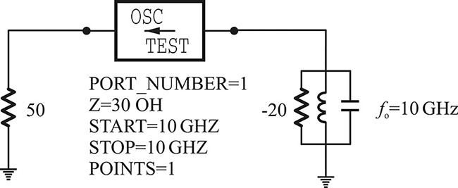
Figure 10P.2 The circuit for Problem 10.2
10.3 (ADS problem) Configure the series oscillating circuit of Example 10.4 in ADS and investigate the effect of the reference impedance on the oscillation condition by varying the reference impedance Z of OscTest for 10, 60, and 110 Ω.
10.4 From the measured spectrum shown in Figure 10P.3, in the following measurement determine the phase noise at a 100-kHz offset from the center frequency; also, calculate the maximum phase deviation ϕ from this offset frequency.
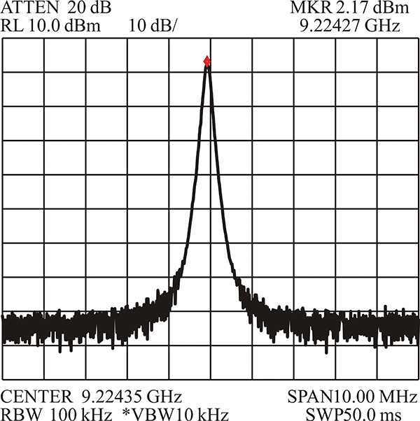
Figure 10P.3 The measured spectrum for Problem 10.4
10.5 Figure 10P.4 shows an oscillator circuit operating at 500 MHz–2 GHz. Simplify this circuit to the basic parallel feedback oscillator circuit and calculate the oscillation frequency and the values x, y, and YL of this parallel feedback oscillator circuit.
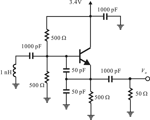
Figure 10P.4 The circuit for Problem 10.5
10.6 A dielectric resonator is used as the bandpass structure shown in Figure 10.76. When the measured QL for |S21| has the insertion loss of IL (dB) at the resonance frequency, prove that the unloaded Q, Qu can be computed as
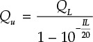
10.7 In the circuit shown in Figure 10P.5, assuming that the impedance of the active part changes linearly with the amplitude of RF current, perform the following tasks:
Figure 10P.5 The circuit for problem 10.7
(1) Set the load impedance value to give maximum output power and calculate the values of L1 and L2 to give this value.
(2) Given that the LD of the active part in Figure 10P.5 is to be replaced using a dielectric resonator coupled to a microstrip, as shown in Figure 10P.6 below, determine the value of θ. Assume the DR is strongly coupled to the microstrip.
10.8 (ADS problem) Using the large-signal model of transistor NE42484, perform the load-pull simulation at 5 GHz at VDS = 2 V and VGS = -0.45 V, which yields about IDS = 20 mA. Determine the feedback circuit that gives optimum output power. Then, verify the output power using ADS.