
Chapter 1. Microwave Integrated Circuits
Chapter Outline
1.1 Classification of Microwave Integrated Circuits
1.2 Microwave Circuits in a Communication System
1.1 Classification of Microwave Integrated Circuits
An active microwave circuit can be defined as a circuit in which active and passive microwave devices such as resistors, capacitors, and inductors are interconnected by transmission lines. At low frequencies, the transmission lines are a simple connection; however, at microwave frequencies they are no longer just simple connections and their operation becomes a complicated distributed circuit element. As a result, a microwave integrated circuit’s classification is based on the fabrication method of the transmission lines used for interconnection.
There are various types of transmission lines in microwave integrated circuits; some common examples are waveguides, coaxial, and microstrip lines. Figure 1.1 shows the transmission lines used in microwave circuits. Although there are special cases of microwave integrated circuits that are composed of coaxial lines and waveguides, in most cases the microwave integrated circuits are formed using planar transmission lines. Therefore, the content of this book is restricted to microwave integrated circuits formed using planar transmission lines, examples of which are microstrip, slot line, and co-planar waveguide (CPW), as shown in Figure 1.2. These planar transmission lines are frequently used in the large-scale production of microwave circuits and generally form the basic transmission lines for microwave circuits.

Figure 1.1 Some common transmission lines used in microwave circuits: (a) coaxial line, (b) rectangular waveguide, and (c) microstrip line

Figure 1.2 Some common planar transmission lines used in microwave circuits: (a) microstrip, (b) slot line, and (c) CPW (co-planar waveguide). They are explained in Chapter 3.
The implementation of planar transmission lines on substrates can be classified into two basic groups: monolithic and hybrid integrated circuits. In monolithic integration, the active and passive devices as well as the planar transmission lines are grown in situ on one planar substrate that is usually made from a semiconductor material called a wafer.
Figure 1.3 shows an example of monolithic integration. Figure 1.3(a) is a photograph of the top side of a wafer and Figure 1.3(b) shows a single monolithic microwave integrated circuit; the identical circuits are repeatedly produced on the wafer in Figure 1.3(a). The monolithic microwave integrated circuit in Figure 1.3(b) is found to contain active and passive devices, and planar transmission lines. The monolithic integration provides a compact-sized circuit and eliminates a significant amount of assembly when building a component or a system. Especially because size is of critical importance in most recent RF systems, monolithic integration is frequently employed to provide a compact component. An advantage of monolithic integration is that it is well suited for large-scale production, which results in lower costs. A disadvantage is that monolithic integration takes a long time to develop and fabricate, and small-scale production results in highly prohibitive costs.
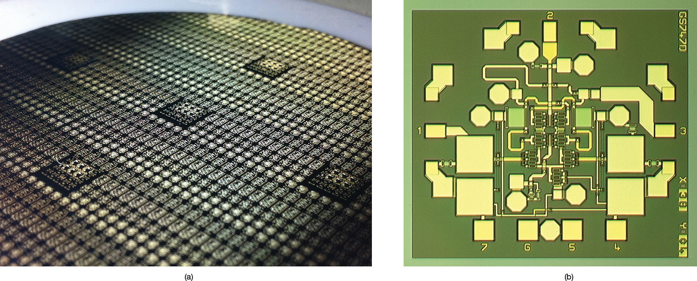
Figure 1.3 Monolithic integration: (a) a wafer and (b) a monolithic microwave integrated circuit on the wafer (28 GHz GaAs pHEMT Gilbert cell up-converting mixer; refer to Chapter 12).
Hybrid integration is a fabrication method in which the transmission lines are implemented by conductor patterns on a selected substrate with either printing or etching, and active and passive devices are assembled on the patterned substrate by either soldering or wire bonding. When implementing transmission lines by conductor patterns on a substrate, careful consideration must be given to the substrate material and the conductor material for the transmission lines because these materials can have significant effects on the characteristics of transmission lines. Hybrid integration is thus classified into three types based on the method by which the lines are formed on the substrate: a printed circuit board (PCB), a thick-film substrate, and a thin-film substrate.
Figure 1.4 shows an example of how connection lines are formed on a PCB substrate. Both sides of the dielectric material are attached with copper cladding that is then etched to obtain the desired conductor patterns. For PCB substrate materials, epoxy fiberglass (FR4), teflon, and duroid are widely used. FR4 substrate (a kind of epoxy fiberglass) can be used from lower frequencies to approximately 4 GHz, while teflon or duroid can be used up to the millimeter wave frequencies, depending on their formation. Generally, all these materials lend themselves to soldering while wire bonding for an integrated circuit assembly is typically not widely used. Furthermore, compared with other methods that will be explained later, a PCB can result in lower costs; its fabrication is easy and requires less time to produce. In addition, production on a small scale is possible without the use of expensive assembly machines; it is easy to fix and could also be used in large-scale production, and is thus widely used.
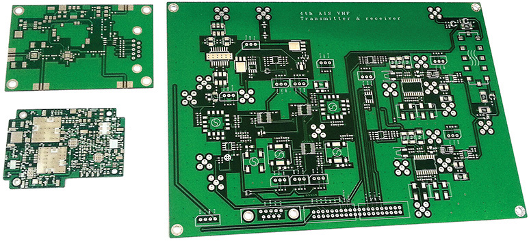
Figure 1.4 A photograph of epoxy fiberglass PCBs. The PCBs on the left are for the X-band and 2 GHz frequency synthesizers using the phase locked loop. The PCB on the right is for the VHF automatic identification system, which has a similar block diagram shown in Figure 1.7. The power amplifier is implemented in a separate block.
Thick-film substrates are produced by screen-printing techniques in which conductor patterns are formed by pushing conductive paste on a ceramic substrate through a patterned screen and then firing printed conductor patterns. The substrate is called thick film because the patterns formed by such techniques are generally much thicker than those formed using thin-film techniques. As a benefit of using screen-printing techniques, multiple screen printings are possible. Dielectric or resistor patterns can also be formed by similar screen-printing techniques using dielectric or resistor pastes. Using an appropriate order of multiple screen printings, it is also possible to form capacitors and resistors on the ceramic substrate. Since the ceramic substrate is more tolerant of heat, it is easy to assemble active devices in the form of chips. On the other hand, considering the lines and patterns formed by this process, the pattern accuracy of thick film is somewhat inferior compared to that of thin film. The costs and development time, on a case-by-case basis, are somewhere between those of the PCB and thin-film processes. Recently, however, the integration based on thick-film technology has become rare because its cost and pattern accuracy are between the PCB and thin-film technology, while thick film is widely used to build multifunction components. A typical example is the package based on LTCC (low-temperature co-fired ceramics) technology.1 Multilayer ceramics and structuring are possible in LTCC technologies. Figure 1.5 shows a photograph of thick-film patterned substrates fabricated using the thick-film process.
1. Refer to Barry LTCC, LTCC Surface Mount T/R Module, at www.barryind.com.

Figure 1.5 A photograph of substrates fabricated by the thick-film process. Identical circuits can be arrayed for efficient production. This circuit is for the mobile communication VCO presented in Chapter 10.
The thin-film technique is very widely used in the fabrication of microwave circuits for military and microwave communication systems. In the case of the thin-film process, a similar ceramic substrate material used in thick film is employed, but compared to the thick-film substrate, a fine surface-finish substrate is used. The most widely used substrate is 99% alumina (Al2O3). Other substrates such as fused silica, quartz, and so on are possible for conductor-pattern generation based on thin-film technologies. The pattern formation on the substrate is created with a photolithographic process that can produce fine tracks of conductor patterns similar to those in a semiconductor process. Since the thin-film substrate is also alumina as in the case of a thick-film substrate, the assembly of semiconductor chips using wire bonding is possible. Thin film compared with PCB and thick film is more expensive, and due to the requirement of fine tracks, a mask fabrication is necessary and the process generally takes longer. Passive components such as resistors and air-bridge capacitors can be implemented using this process. In addition, integrated circuits produced by the thin-film process require special wire bonders and microwelding equipment for assembly. Compared to the monolithic integration process, the thin-film process tends to be cheaper in terms of cost, but compared to MMIC, the assembled circuit using the thin-film patterned substrate is difficult to characterize precisely because of unknown or poorly described parasitic circuit elements associated with the assembly methods such as wire bonding and die attach. Before the emergence of MMICs (monolithic microwave integrated circuits), thin-film technology was the conventional method for building microwave-integrated circuits (MICs). Figure 1.6 is a photograph of thin-film circuits fabricated with the thin-film technique.

Figure 1.6 A photograph of substrates produced by the thin-film process. From top left to bottom right, they are filter, phase shifter, power amplifier (presented in Chapter 9), path-switching circuit by assembly, power divider, and 50 Ω lines.
The choice of integration method depends on the application and situation, taking into account several factors mentioned previously, such as the operating frequency of the integrated circuit, the types of semiconductor components (chip or packaged), the forms of the passive components, large-scale fabrication costs, and method of assembly. These factors should all be considered when selecting the optimum method of integration. For a description of microwave-patterned substrate fabrication, assembly with wire bonding and soldering, and packaging, see reference 1 at the end of this chapter. The book provides general information about microwave-circuit fabrications. Table 1.1 provides a comparison of the hybrid integrations described previously.

Now we will consider the application of the planar transmission lines such as microstrip, slot, and CPW to the monolithic and hybrid integration technologies. Microstrip lines are the most widely used transmission lines for both monolithic and hybrid integration technologies. In microstrip lines, the top conductor pattern is usually connected to the ground by a through hole or a via hole. Thus, the back-side process for the through-hole or via-hole fabrication is essential to building a circuit based on microstrip lines. This back-side process is inconvenient especially in the monolithic integration. In hybrid integration, the holes can be fabricated through simple mechanical drilling for a PCB case and through laser or ultrasonic drilling for thick- and thin-film cases. Then, plating the fabricated holes completes the fabrication of a through or via hole. However, to fabricate via holes in monolithic integration, a wafer that typically has a normal thickness of about 600 μm should be polished down to about 100 μm thickness. Current technology does not support via-hole fabrication beyond 100 μm. In Figure 1.2, we can see that the CPW and slot lines do not need the back-side metallic ground and they eliminate the need for any additional back-side metallization process. The CPW is very helpful in monolithic integration and is widely used to build MMICs without vias. However, the discontinuities of CPWs are not well understood compared to those of microstrip lines and the integration based on a CPW is not as popular as that based on a microstrip. The various discontinuities of microstrip and slot lines, CPWs, and planar transmission lines are covered in reference 2 at the end of this chapter.
1.2 Microwave Circuits in a Communication System
Microwave integrated circuit classification has been discussed previously. The microwave integrated circuit was classified according to the method of implementing the planar transmission lines for the purpose of connecting active and passive devices. The functions of microwave integrated circuits vary greatly and we will now consider several important microwave integrated circuits, the designs of which will be discussed in later chapters. Some examples of these circuits are low-noise amplifiers (LNA), power amplifiers (PA), oscillators, mixers, directional couplers, switches, attenuators, and filters, among a host of other microwave-integrated circuits. Among these, directional couplers, switches, attenuators, filters, and so on, are basically passive microwave circuits, although they are very widely used. Thus, they are not covered in this book because they are considered to be outside its scope. In addition, although components such as switches, variable attenuators, phase shifters, and other control circuits are important and are composed of semiconductor devices, they are generally not regarded as the basic building blocks of a wireless communication system. Therefore, this book will only cover low-noise amplifiers, power amplifiers, oscillators, and mixers, which are the most widely used circuits in the construction of wireless communication systems. The basic design theory of these circuits as well as the devices related to them will be explained in this book.
As an example of a wireless communication system, Figure 1.7 shows a block diagram of an analog cellular phone handset (Rx frequency is 869–894 MHz and Tx frequency is 824–849 MHz).2 A general transceiver used for the transmission and reception of analog signals (usually voice) has a similar block diagram that is shown in Figure 1.7. A weak RF signal with a typical power level of about –100 dBm (0.1 nW) received from an antenna first goes through a filter called a diplexer and the signal is received only in the receiver frequency band. The filtered signal is too weak for direct demodulation or signal processing, and a low-noise amplifier (LNA) with a gain of 20–30 dB is required to amplify the received signal. Too much gain may cause distortion and an LNA with a gain of 20–30 dB is usually employed. Chapter 8 provides a detailed explanation of the design of an LNA.
2. Refer to AMPS (Advanced Mobile Phone System) standard.
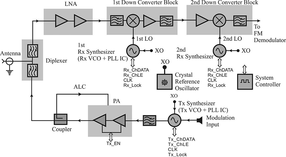
Figure 1.7 A block diagram of an analog mobile phone handset (AMPS standard). Tx_EN stands for Tx enable and ALC stands for automatic level control. Tx_ and Rx_data are required to set the programmable frequency dividers in Tx and Rx synthesizers. LE stands for Load Enable. When LE is high, the digital channel data are loaded to the corresponding programmable frequency divider in PLL IC. Synthesizers are explained in Chapter 11. Lock signal indicates that the synthesizer using PLL is in a locked state.
Next, because the received signal frequency is so high, the first mixer shown in Figure 1.7 translates the carrier frequency to a lower frequency band called first IF (intermediate frequency). A double-conversion superheterodyne receiver is more widely used than a single-conversion super heterodyne receiver in a communication system. The filter in front of the first mixer again suppresses both the image frequency signal and other signals at the outside of the receiving frequency band. Since multiple users in service are using the same frequency band, multiples of other user signals generally coexist with the signal in the first IF. Intermodulations among the multiple signals are one of the crucial issues in mixer design. Chapter 12 describes the typical topologies of various mixers for suppressing such spurious signals. In order to filter out possible spurious signals that appear at the first mixer output, the signal is passed through a narrow bandpass filter that has a bandwidth of about the signal bandwidth. The first IF filter removes many unwanted spurious signals although it may not be completely sufficient. The first IF output is converted again through the second mixing. Now the center frequency of the second IF is low enough, the highly selective filter is available, and the spurious signals can be sufficiently suppressed through the second IF filter. In addition, the signal frequency is low enough and can be demodulated for the recovery of the original signal. The demodulator is an FM demodulator and is almost the same as the FM demodulator that is commercially popular.
Note that the mixer requires the input signal from a local oscillator (LO) for the translation of the signal frequency to the IF. The two LO signals are supplied from the two Rx-synthesizers and each Rx-synthesizer consists of a voltage-controlled oscillator (VCO) and a commercial PLL (phase-locked loop) IC (integrated circuit). Since the frequency of most VCOs is not stable enough to be used in such communication systems, the frequency of a VCO must be stabilized using a stable crystal oscillator (XO in Figure 1.7) with a typical temperature stability of 2 ppm (parts per million) and a phase-locked loop (PLL). Furthermore, the LO frequency should be moved up and down according to the base station commands. Such frequency synthesis and stabilization can be achieved by a phase-locked loop (PLL). To build a frequency synthesizer using PLL, the VCO frequency as well as the crystal oscillator frequency must be divided by appropriate programmable frequency dividers in the PLL IC. The signals CLK, Rx_ChDATA, Rx_ChLE, and Rx_Lock, shown in Figure 1.7, are the digital signals between the PLL IC and the system controller. The clock signal CLK is used for the timing reference signal that is generated by the system controller using the crystal oscillator. Rx_ChDATA sent from the controller represents the digital data to set the programmable frequency dividers. The signal Rx_ChLE selects the corresponding programmable divider for Rx_ChDATA to be loaded among several frequency dividers in the PLL IC. When phase lock is achieved, the PLL IC sends the signal Rx_Lock to the system controller to inform the phase lock completion. The two Rx synthesizers are necessary for the double-conversion superheterodyne receiver. The commercial PLL IC generally includes the necessary components to achieve the phase lock for two VCOs in a single PLL IC. Thus, the LO signal for the second conversion is similarly synthesized using a single PLL IC. The design of the Tx and Rx VCOs in Figure 1.7 as well as the other microwave VCOs are described in Chapter 10, while the PLL’s operation is explained in Chapter 11.
In the transmission operation, the modulation input signal (usually voice) goes to the modulation input of a Tx synthesizer. The Tx synthesizer is similarly composed of a VCO and a PLL IC. Through the PLL IC, the desired carrier center frequency is similarly synthesized as in the Rx synthesizer. The digital signals CLK, Tx_ChDATA, Tx_ChLE, and Tx_Lock are similarly interpreted as in the Rx synthesizer. The modulation signal has a generally higher frequency than the PLL loop bandwidth and thus can modulate a VCO without the effects of a PLL. Therefore, the frequency-modulated (FM) signal appears at the Tx synthesizer output with the synthesized carrier frequency. The modulated signal then passes through the bandpass filter that removes unnecessary or spurious signals. The average output power level of the modulated signal is generally low; thus, in order to obtain the desired RF power output level, the signal must be amplified by a power amplifier (PA) whose typical maximum output power level is about 1W. The function ALC (Automatic Level Control) is generally built in to control the transmitting power level. When a user is close to the base station, the transmitting power level is set to low; otherwise, it is set to high for a better quality of communication. The PA output signal is then passed through a diplexer without affecting the receiver and radiated via the antenna. A power amplifier is important in this type of communication system because it consumes most of the DC power supplied from a battery. Furthermore, because a power amplifier operates in large-signal conditions, significant distortion arises. In Chapter 9, we will discuss the design and linearity evaluation of a power amplifier.
Given the preceding discussion, the key circuits in building a communication system are a low-noise amplifier, a power amplifier, oscillators, and mixers. With that in mind, this book will discuss in detail the design and evaluation method of these circuits.
1.3 Summary
• Microwave integrated circuits can be classified according to the fabrication method of the patterned substrate and in terms of monolithic and hybrid integration. Hybrid integration can be further classified into integrations based on PCB, thick film, and thin film. In the selection of integration, one type cannot be said to be superior to the other; the choice is made depending on the application and given situation, and by taking into consideration several factors such as cost, time, pattern accuracy, and assembly.
• Among active microwave circuits, the most commonly used building blocks for wireless communication systems or other systems, such as repeaters, transponders, and radars, are amplifiers, oscillators, and mixers.
References
1. T. S. Lavergetta, Microwave Materials and Fabrication Techniques, Dedham, MA: Artech House, Inc., 1984.
2. K. C. Gupta, Microstrip Lines and Slot Lines, 2nd ed. Dedham, MA: Artech House, Inc., 1996.
Problems
1.1 A waveguide generally has lower line loss than a microstrip. An SIW (substrate integrated waveguide) can be considered as the planar version of a waveguide. How is an SIW configured using a substrate?
1.2 Find the TR (transmission and receiving) module example built using a LTCC on the Web site www.barryind.com.
1.3 How is the ALC in Figure 1.7 constructed?
1.4 Refer to the FM demodulator IC SA605, which is used to demodulate an FM signal. Explain how the FM signal is demodulated using its block diagram.
1.5 Refer to the Web site of vendors of PLL IC such as Analog Devices Inc. or other companies. Explain the synthesizer data bus shown in Figure 1.7.
1.6 How can the PLL be modulated? Explain how to set the PLL loop bandwidth by taking the bandwidth of a bandlimited modulation signal into consideration.