J
jack A socket containing a number of spring-loaded contacts which mate with the corresponding contacts of a plug inserted in the jack. The contacts within the jack can be arranged to make or break particular circuits when the plug is inserted as shown in the graphical symbols in Figure J.1. Plugs and jacks are extensively used in telephone switchboards and in broadcasting to permit rapid connections to be made to equipment or circuits.
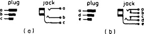
Figure J.1 (a) A three-pole plug and jack connecting two wires and earth and (b) a break-jack. At (b) the contact between a and b and between c and d is broken when the plug is inserted
jamming Deliberate transmission of radio signals to interfere with the reception of other signals.
jitter General term for sudden irregular departures from the ideal value of a parameter such as the phase, amplitude or pulse duration of a signal. In TV signals jitter can cause errors in synchronising and these can lead to erratic movements in the displayed picture.
JK bistable A bistable circuit with two inputs labelled J and K. When the J input is at its logic-1 state, the output (see Figure J.2) takes up its logic-1 state. When the J input is at its 0-state it has no effect on the output. When the K input is at its logic-1 state the output takes up its 0-state, but when the K input is at its logic-0 state it has no effect on the output.

The behaviour of the J and K inputs is thus similar to that of the R and S inputs of an RS bistable but the JK bistable has the advantage that if logic-1 signals are applied simultaneously to the two inputs the output is predictable. In fact every time the simultaneous logic-1 inputs are applied the output of the bistable goes to the complementary state.
Johnson noise Same as thermal noise.
Joint Photographic Experts Group (JPEG) A standard for the storage of true-colour bitmaps such as those obtained from colour photographs using a scanner. The JPEG standard uses Fourier Transform technology to sacrifice fine detail selectively in order to reduce the storage requirements. The degree of compression, however, is controlled by the JPEG file creator who chooses a quality factor expressed as a percentage. At high settings there is little detail loss, although worthwhile space savings may be made; at lower settings deterioration in image quality is more visible and there are greater space savings. Results vary with subject matter, but for many photographs a quality setting of 87 per cent results in a JPEG file about 10 per cent of the size of the original uncompressed bitmap with imperceptible deterioration in image quality at normal magnifications. A purpose-designed integrated circuit is available which decodes JPEG images considerably faster than a computer can. See also MPEG.
Joule effect The heating effect generated by an electric current in a conductor by virtue of its resistance. Joule’s law states that the rate of heat generation is proportional to the square of the current.
joystick A control capable of movement in two mutually-perpendicular directions. Such a control may be used to adjust the position of the cursor of a VDU.
jump In computing, the transfer of control to a different area in memory. This contrasts with the processor’s normal sequential execution of the instructions held in memory.
junction In a semiconductor device a transition region between two regions of different types of conductivity, e.g. a pn junction is the transition region between a p-region and an n-region.
When a pn junction is forward biased as indicated in Figure J.3(a), the p-region being positive with respect to the n-region, a considerable current crosses the junction. This current is carried by majority carriers, i.e. holes from the p-region (which move to the right) and electrons from the n-region (which move to the left). This forward current increases rapidly with increase in applied voltage.

Figure J.3 (a) Movements of majority carriers in a forward-biased pn junction and (b) movement of minority carriers in a reverse-biased junction
If, however, the battery is reversed the majority carriers move away from each other leaving the junction region deficient in carriers: it is then known as a depletion layer. The only current which crosses a reverse-biased junction is a very small one composed of minority carriers, electrons from the p-region (which move to the right) and holes from the n-region (which move to the left). This small leakage current is largely independent of the applied reverse voltage.
junction diode A pn junction employed because of its unilateral conductivity. Such diodes are extensively used for rectification, detection and in digital circuitry. The graphical symbol for a junction diode is given in Figure J.4.
![]()
Figure J.4 Graphical symbol for a diode. The end marked + is that which goes positive when the diode conducts
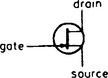
junction-gate field-effect transistor (JUGFET) A field-effect transistor in which the gate forms a pn junction with the channel. A simplified structure of an n-channel JUGFET is given in Figure J.5. It consists of a crystal of n-type silicon with ohmic contacts provided by highly-doped (n+) regions near the two ends: these provide the source and drain connections to the external circuit. A region of p-type conductivity is formed (e.g. by diffusion) between the ohmic contacts: this provides the gate connection.

Figure J.5 Simplified diagram showing the structure of an n-channel junction-gate field-effect transistor
Current flowing longitudinally between the n+ regions is carried by the free electrons of the n-type channel. The number of electrons available to act as charge carriers is, however, dependent on the gate bias. The more negative (with respect to the source voltage) the gate is made the greater is the area of the depletion layer surrounding the p-region and the smaller the number of electrons available to carry the longitudinal current. In fact the channel can be cut off completely by a sufficiently-great reverse bias on the gate, the depletion layer then occupying the whole of the cross section of the channel.
Because the pn junction is reverse-biased during normal operation of the FET the transistor has a very high input resistance. The channel of a JUGFET may have more than one gate. A connection to the substrate can also provide a second input terminal although it is not usually as sensitive as the normal gate terminal. JUGFETs operate in the depletion mode and the graphical symbol for an n-channel device is given in Figure J.6.
junction transistor A transistor containing a pn junction in its structure. This definition includes a junction-gate field-effect transistor but the term is generally used to mean a bipolar transistor as opposed to a field-effect transistor.