N
NAND gate (NOT-AND gate) A logic gate which gives a logic-0 output when, and only when, all the input signals are at logic 1. It may be regarded as an AND gate followed by a NOT or logic negating stage as suggested by the graphical symbol shown in Figure N.1. See logic level.
natural air cooling Same as convection cooling.
natural frequency Of an oscillatory system, the frequency of free oscillations. Thus it is the frequency at which the system oscillates when shock-excited. A system can have more than one natural frequency and the natural frequency of an antenna is the lowest frequency at which it resonates without the addition of inductance or capacitance.
natural period The reciprocal of the natural frequency.
n-channel metal-oxide-semiconductor (NMOS) A form of construction for logic monolithic integrated circuits using n-channel field-effect transistors. These have the advantage over PMOS of higher speed of operation (the charge carriers, being electrons, have higher mobility than holes) and have largely replaced PMOS.
Near Instantaneous Compression and Audio Multiplex (NICAM) A digital coding system for the inclusion of sound or data signals within a television broadcast transmission. The signal, typically two-channel stereo, is quantised to 14 bits and compressed to 10 bits. Left- and right-channel data is sent alternately in blocks of 32 11-bit (10 data bits plus one parity bit) words, each lasting 1 ms and containing, with control and framing codes, 728 bits. The NICAM carrier is quadrature modulated by the interleaved and scrambled binary data and transmitted at low level adjacent to the normal f.m. sound carrier.
negate In logic to perform the NOT operation. Thus an AND gate followed by a negating operation becomes a NOT-AND or NAND gate. The symbol for negation is shown in Figure N.2.
negative AND gate Same as NAND gate.
negative feedback (NFB) Feedback in which the signal returned to the earlier stage in the amplifier opposes the input signal at that point. Negative feedback has the effect of reducing the gain of that portion of the amplifier included within the feedback loop. It also improves the linearity and makes the frequency response more level.
Negative feedback has an effect on the output impedance of that stage of the amplifier from which the signal is derived and on the input impedance of the stage at which it is re-introduced. The effect on output impedance depends on whether the feedback signal is proportional to the output voltage (see voltage feedback) or to the output current (see current feedback). The effect on input impedance depends on the way in which feedback signal is re-introduced into the amplifier: if it is connected in series with the input signal it increases input impedance; if it is connected in parallel with the input signal it reduces the input impedance.
Negative feedback is extensively used in the design of electronic equipment. It can be used to give an amplifier a required value of gain, a required value of linearity, a required shape of frequency response (by making the feedback path frequency-discriminating) and required values of input and output impedance. These properties are obtained by suitable choice of passive components in the feedback circuit and they are therefore independent of the properties of the active devices contained within the feedback loop—a very useful feature in the mass production of electronic equipment.
negative image An image in which white areas are reproduced as black and black areas as white as in a negative photographic film. The effect can occur in TV images, when, for example, the picture tube has low emission.
negative logic A computer or data processing system in which the more negative of the two voltages selected as the logic levels is designated the 1 state.
negative modulation In TV transmission amplitude modulation in which increased picture brightness results in decreased carrier amplitude. This is the system of modulation used in the British 625-line and in most of the world’s television systems.
negative OR gate Same as NOR gate.
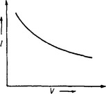
negative resistance Property of a device in which an increase in applied voltage brings about a decrease in the current through it. The current-voltage characteristic for such a device has a negative slope as shown in Figure N.3. Electron tubes can be operated so as to produce a region of negative resistance (see dynatron). A semiconductor example with a similar region is the tunnel diode. A most useful property of a negative-resistance device is that a simple oscillator can be made by connecting a parallel resonant circuit across it.
NEITHER-NOR gate Same as NOR gate.
neon tube A gas discharge tube containing two electrodes and filled with neon at low pressure. When a voltage exceeding the ionisation voltage is applied between the electrodes a discharge occurs giving a characteristic red glow. Such tubes are used in neon signs and as indicators in electronic equipment. When the discharge occurs the voltage across the electrodes remains constant and the tube can therefore be used as a voltage reference. The graphical symbol for a neon tube is given in Figure N.4.
neper The basic unit of a logarithmic scale used to express ratios of voltages, currents and analogous quantities. The neper is based on the use of natural logarithms and is named after their inventor, John Napier. Two voltages V1 and V2 are related by n nepers when loge(V1/V2) = n. The number of nepers is simply the natural logarithm of the voltage ratio.
In conditions of equal impedance (as is usual for input and output quantities in telecommunications) a voltage or current ratio is equal to the square root of the corresponding power ratio. Hence
By extension, this formula may be applied when the power ratio is not the square of the ratio of the corresponding voltages or currents. It is then important to specify the convention adopted and to indicate the sphere of validity of the usage. The neper may by used to express levels of quantities such as voltage and current in the same way as the decibel.
(1) A system of inter-connected components chosen and arranged to give specific electrical characteristics. A network containing no source of power is termed passive and one containing one or more sources is known as an active network. If the values of the components forming the network are dependent on the current in them the network is termed non-linear but if the values are independent of current the network is linear.
(2) In computing two or more computers connected together to facilitate the exchange of data. Computer networks are generally classified as local area networks if the computers concerned are located on the same premises or as wide area networks if they are on separate premises and the connection requires the use of telecommunications lines. See local area network, wide area network.
network transfer constant Same as image transfer constant.
neutralisation Use of a balancing network to counteract the feedback between the input and output terminals of an active device which occurs via the internal capacitance. The internal feedback causes instability when input and output circuits are tuned to the same frequency and neutralisation is used to enable, for example, transistors in radio receivers to give stable IF amplification. A typical circuit is given in Figure N.5: the neutralising capacitor Cn is adjusted to cancel the effect of the collector-base capacitance.

neutrodyne A method of neutralisation developed by Hazeltine in the USA.
neutron An elementary atomic particle with no charge and similar mass to the proton. It is a constituent of all atomic nuclei except that of hydrogen.
n-gate thyristor A thyristor which is switched to the on-state by a negative signal applied between gate and anode, the gate being a connection to the n-region nearest the anode. It is normally a reverse-blocking thyristor, i.e. one which cannot be switched to the on-state when the anode is negative with respect to the cathode. The graphical symbol for the n-gate thyristor is given in Figure N.6.
nickel-cadmium cell A secondary cell in which the anode consists of a mixture of nickel oxide and hydroxide, the cathode is of cadmium and the electrolyte is of potassium hydroxide. Its properties are similar to those of the nickel-iron cell. It is widely used in portable electronic equipments.
nickel hydride cell A type of dry battery used in some portable equipment, which offers approximately twice the capacity of nickel cadmium cells.
nickel-iron cell A secondary cell in which the anode consists of a mixture of nickel oxide and hydroxide, the cathode is of iron and the electrolyte is of potassium hydroxide. This is an alternative to the lead-acid cell and has the advantage that the nickel-iron cell will operate satisfactorily at temperatures as low as −30°C. On the other hand it is more expensive than the lead-acid cell and its EMF is only 1.2 V.
Nipkow disk Mechanical scanning device used in early experiments in TV. It consists of a disk containing a number of apertures arranged on a spiral path. The scene to be televised is illuminated by light which passes through these apertures so that, as the disk revolves, the scene is scanned. Light reflected from the scene is picked up by photocells the output of which is the required picture signal. The system was used in the BBC 30-line television experiments in the late 1920s.
(1) In a network a point where three or more elements are connected (internal node) or where signals are applied to or withdrawn from an element (external node). For example the network shown in Figure N.7 has six nodes, two internal and four external. External nodes are alternatively known as terminals.

(2) Of a standing wave, a point or plane at which a specified variable has a minimum value. Thus nodes on a transmission line are points at which voltage or current is a minimum. For a bowed string nodes are points at which the amplitude of vibration is a minimum. See antinode.
noise In general any unwanted signals within the useful frequency band of a communications system which tend to obscure the wanted signal. This is a wide definition and embraces a variety of man-made noises such as mains hum, signals from other channels arising from inadequate selectivity or poor image rejection, cross modulation, etc; it also includes naturally-generated signals arising from lightning flashes. Signals from such causes are better termed interference so that the term noise is reserved for signals which arise in components and active devices and are known as random noise. Such signals are termed noise because they are heard as undesired sound when reproduced by an acoustic transducer but the term is retained for signals which cause spurious detail on the screen of a cathode ray tube.
Random noise from components is known as thermal noise or Johnson noise and from active devices is known as shot noise and partition noise. Even if all sources of man-made noise can be eliminated there still remains random noise and the level of this noise determines the amplitude of the weakest signal which can be successfully transmitted through a communications system. Wanted signals must exceed the noise level by a margin which ensures that the noise does not impair the intelligibility of the signal unduly or the enjoyment of the programme. Thus the noise level and the signal-to-noise ratio are two important properties of a communications system.
noise factor (or noise figure) Of a device, a measure of the noise it introduces. More specifically it is the ratio of the signal-to-noise ratio at the output of the device to the signal-to-noise ratio at the input and is usually expressed in dB. An ideal, i.e. noise-free, device thus has a noise factor of unity (0 dB).
noise generator A device for generating a standard noise signal which can be used for the measurement of noise factor. In such generators the shot noise in a saturated diode is often employed as the primary source of noise.
noise limiter In a radio or TV receiver a circuit used to reduce the effect of impulsive noise signals on the sound or picture output. Typically the circuit includes a series diode which is situated at the output of the detector and is so biased that it remains conductive for all normal amplitudes of sound or video signals but becomes non-conductive, so interrupting the wanted signal, for the duration of any noise pulse exceeding a pre-determined amplitude. The resulting interruptions are normally so brief that their subjective effect is negligible.
noise temperature At a given pair of terminals and at a given frequency the temperature of a resistance which gives the same noise power per unit bandwidth as the noise to be measured. The standard reference temperature for noise measurement is 290°K.
non-composite colour-picture signal (US) In TV the signal which comprises full colour-picture information including the colour burst but excluding the synchronising signals.
non-composite signal (US) Same as picture signal.
non-conjunction gate Same as NAND gate.
non-equivalence gate Same as exclusive-OR gate.
non-linear circuit element A circuit element for which the significant property is dependent on the current flowing through it or the voltage across it. An example is a non-linear resistance.
non-linearity distortion General term embracing all the forms of distortion which result from non-linearity of the input-output characteristics of a system, equipment or component, e.g. amplitude distortion, harmonic distortion and intermodulation distortion. The significant feature of non-linearity distortion is that it is dependent on signal amplitude.
non-linear network See network.
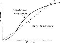
non-linear resistance A resistance for which the current is not directly proportional to the applied voltage. Such a resistance may have a current-voltage characteristic of the form shown in Figure N.8. For comparison the characteristic for a linear resistor (i.e. one which obeys Ohm’s law) is shown as a dashed line.
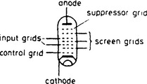
nonode An electron tube with seven grids between cathode and anode. The first grid (nearest the cathode) is a control grid, grids 2, 4 and 6 are screen grids 3, 5 and 7 are suppressor grids. The arrangement is shown in Figure N.9. The tube was used in FM receivers as a self-limiting phase-difference discriminator and grids 3 and 5 are fed with FM signals from the primary and secondary windings of an IF transformer. The control grid is given a steady bias and suppressor grid 7 is connected to cathode to suppress tetrode kink. The three screen grids are commoned and connected to a low voltage such as 30 V. The limiting action stems from the use of suppressor grids as input electrodes. The signals swing the anode current between zero and the value set by the control-grid bias. Increase in the amplitude of the input signals can produce no corresponding increase in anode-current swing.
non-volatile A term used to describe any form of memory which retains the data it is storing when the equipment is switched off or loses its power supply for some other reason. Under these circumstances the contents of normal RAM is lost. Examples of non-volatile memory include battery-backed RAM and various forms of EPROM.
NOR gate (NOT-OR gate) A logic gate which gives a logic-0 output when one or more of the input signals is at logic 1. It may be regarded as an OR gate followed by a negating stage as shown by the graphical symbol in Figure N.10. See logic level.
Norton’s theorem If an admittance Y’ is connected between any two points of a linear network the voltage across it is given by I/(Y + Y′), where I is the short-circuit current and Y is the admittance measured between the points before Y′ was connected.
NOT-AND gate Same as NAND gate.
NOT-BOTH gate Same as NAND gate.
notch filter A bandstop filter for which the stop band is extremely narrow. Such filters are used for reducing interference which is confined to a single frequency (e.g. heterodyne interference) or to a narrow band of frequencies. The frequency response for a notch filter is illustrated in Figure N.11.

NOT gate A logic gate with a single input and a single output, which gives a logic-0 output when the input is at logic 1, and a logic-1 output when the input is at logic 0. It is often termed a logic negator or inverter.
npin transistor A type of bipolar transistor in which the base and collector regions are separated by a region of intrinsic material.
npn transistor See bipolar transistor.
NTSC colour television system A compatible colour TV system pioneered by the National Television Systems Committee in USA in which the luminance signal is transmitted by amplitude modulation of the vision carrier and two chrominance signals are transmitted simultaneously by quadrature modulation of a subcarrier, the total bandwidth being the same as that of a black-and-white system using the same line standards. A colour burst is included in the back porch to facilitate decoding of the colour subcarrier.
This is the system used in USA and a number of other countries. The PAL system used in UK and a number of other countries is a development of the NTSC system. See PAL and SECAM systems.
n-type semiconductor An extrinsic semiconductor in which the free-electron density exceeds that of the hole density. Thus the negative charge carriers outnumber the positive charge carriers and current flowing through such materials is due to movement of negative charge carriers.
nuvistor Miniature electron tube of rigid construction with small electrodes and electrode clearances designed for high reliability.
Nyquist diagram Of a feedback amplifier a graph in rectangular coordinates showing the real and imaginary components of the ratio μ/β, where μ is the gain of the amplifier and β is the fraction of the output voltage fed back. Such a diagram, if plotted for a very wide frequency range, can be used to predict whether the amplifier will be stable.