
Chapter 11
AC–DC–AC Converters for Distributed Power Generation Systems
Marek Jasinski, Sebastian Stynski, Pawel Mlodzikowski and Mariusz Malinowski
Faculty of Electrical Engineering, Warsaw University of Technology, Warsaw, Poland
11.1 Introduction
Indirect AC–DC–AC converters consist of two connected voltage source converters (VSCs) as presented in Figure 11.1. The AC–DC–AC is a connection through a DC-link of two single-phase, three-phase, or multiphase AC circuits with different voltage amplitude ![]() , frequency
, frequency ![]() , or phase angle
, or phase angle ![]() . The major application of AC–DC–AC converters is in adjustable speed drives. However, recently, these converters have begun to play an increasingly important role in distributed power generation systems (DPGSs) and sustainable AC and DC grids.
. The major application of AC–DC–AC converters is in adjustable speed drives. However, recently, these converters have begun to play an increasingly important role in distributed power generation systems (DPGSs) and sustainable AC and DC grids.
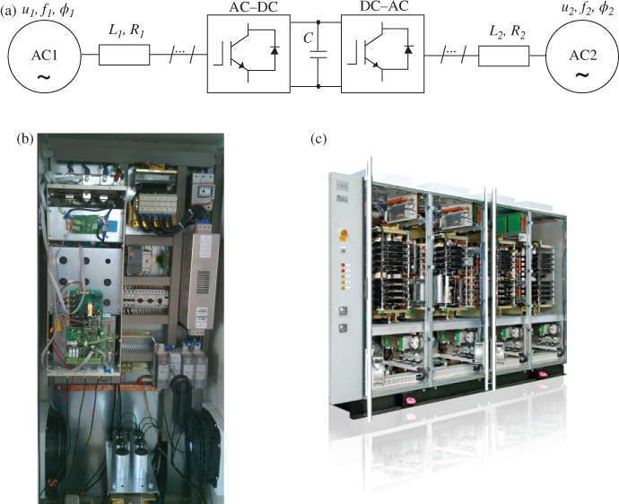
Figure 11.1 AC–DC–AC indirect converter (a) general block scheme (b) photo of commercially available AC–DC–AC converters manufactured by TWERD type: MFC810ACR, (c) photo of commercially available AC–DC–AC converters manufactured by ABB type: PCS6000 [1 2]
There are several possibilities for an AC–DC–AC converter configuration [1–21]. In this chapter, only the most promising bidirectional topologies are presented and discussed. Recently, bidirectional AC–DC–AC converters are available on the market for different voltage levels [1 2].
Both parts of the converter (i.e., AC–DC and DC–AC) can be controlled independently. However, in some cases, there is a need for improving the control accuracy and dynamics. Therefore, it is useful to use an additional link between both control algorithms, which operates as an active power feedforward (APFF). The APFF gives information about the active power on one side of the AC–DC–AC converter to the other side directly, and consequently, the stability of the DC voltage is improved significantly.
11.1.1 Bidirectional AC–DC–AC Topologies
There are several configurations possible for three-phase to three-phase AC–DC–AC full-bridge converters, which can connect two AC systems. The most popular is a two-level converter, as shown in Figure 11.2(a), which is used mostly in low voltage and low-power or medium-power applications, for example, adjustable speed drives. On the other hand, three-level diode-clamped converters (DCCs) [11–12] and flying capacitor converters (FCCs) [4 6, 7] (Figure 11.2(b and c)) are becoming increasingly popular, but usually in the medium-voltage range for medium- and high-power applications [4], for example, marine propulsion, renewable energy conversion, rolling mills and railway traction. There are several advantages of multilevel converters, such as lower voltage stress of components, low current and voltage, total harmonic distortion factor and reduced volume of input passive filters. The main differences among the mentioned multilevel topologies are as follows [4]:
- DCC is the most popular topology and needs fewer capacitors. However, for higher voltage levels, it requires serially connected clamping diodes, which increases the losses and switching losses. In addition, for higher voltage levels, the DC capacitor voltage balancing cannot be achieved with classical modulations.
- FCC is less popular because it needs initialization of the FC voltage, and higher switching frequency is required (greater than 1.2 kHz, whereas for high-power applications the switching frequency is usually between 500 and 800 Hz) in high-power applications because of the FC limits, that is, capacitance versus volume.
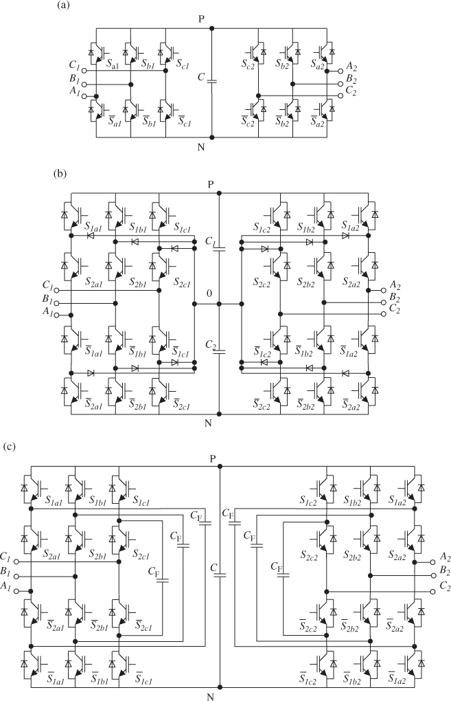
Figure 11.2 Fully controlled three-phase/three-phase, transistor-based AC–DC–AC converter: (a) two-level (2L-3/3), (b) three-level DCC (3L-DCC-3/3) and (c) three-level FCC (3L-FCC-3/3)
Another group of AC–DC–AC converters are simplified topologies obtained by reducing the number of power electronic switches [8–10]. These attempts were based on the idea of replacing one of the semiconductor legs with a split capacitor bank and connecting a one-phase wire to its middle. In simplified topology, the lower number of switching devices, compared with that of a classical three-phase converter, corresponds to a reduced number of control channels and insulated-gate bipolar transistor (IGBT) driver circuits. Thus, connecting a three-phase AC system to a single-phase AC system is possible by using a single-standard three-leg integrated power module as the AC–DC–AC converter, as shown in Figure 11.3(a).
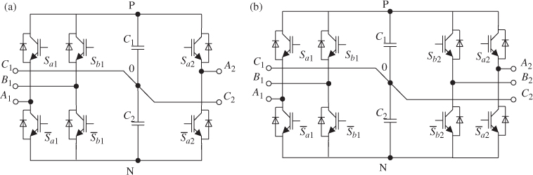
Figure 11.3 Simplified AC–DC–AC converters: (a) two-level three-phase/one-phase (S2L-3/1) and (b) two-level three-phase/three-phase (S2L-3/3)
The same concept can be used to simplify an AC–DC–AC converter by connecting one three-phase system to another using only one additional leg, as is shown in Figure 11.3(b). Despite the advantages of these solutions, there is a necessity to develop new modulation techniques and to keep the DC voltage significantly high in order to maintain all nominal phase-to-phase converter voltages, which places higher voltage stress on the converter semiconductor devices.
This problem can be solved by application of a three-level DCC. When this technology was emerging in industry, not a single integrated power module product for three-level devices was available. Today, manufacturers are selling easy-to-use integrated half-bridge power modules with clamping diodes. New compact devices make it easier to improve the topology with a split capacitor in the DC-link. Thus, the improved topology of a simplified AC–DC–AC converter is shown in Figure 11.4, for applications of three-phase to single-phase, as well as for three-phase to three-phase systems. The first topology is dedicated only to low-power applications, whereas the second is devoted to low- and medium-power applications.
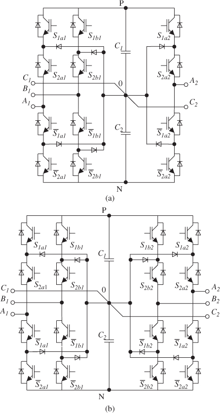
Figure 11.4 Simplified DCC AC–DC–AC converters: (a) three-phase/one-phase (S3L-DCC 3/1) and (b) three-phase/three-phase (S3L-DCC 3/3)
The simplified three-level DCC has several advantages compared with that of a simplified two-level topology [13]: reduction of machine torque pulsations (mechanical stress in cases where generator/motor application is decreased), additional zero vectors, and reduction in size of passive filters on the AC side.
11.1.2 Passive Components Design for an AC–DC–AC Converter
This section is devoted to the methods of passive components of an AC–DC–AC converter design. Among them, there are input filters (L or LCL), DC-link capacitors, and flying capacitors (FCs), which have a significant impact on the size, weight and final price of the AC–DC–AC converter.
11.1.3 DC-Link Capacitor Rating
In the literature, many design procedures [17–20] for DC-link capacitors are presented, where the minimum capacitance value is designed to limit the DC-link voltage ripple at a specified level. With the assumption of a balanced three-phase system and of ideal power electronics switches, the DC capacitor current can be expressed as:
where ![]() is the capacitance of a DC capacitor,
is the capacitance of a DC capacitor, ![]() is the DC voltage,
is the DC voltage, ![]() is the DC current,
is the DC current, ![]() is the load DC current,
is the load DC current, ![]() are letters of AC circuit phase,
are letters of AC circuit phase, ![]() and
and ![]() are the AC circuit phase instantaneous current and switching states at the appropriate phases, respectively, and
are the AC circuit phase instantaneous current and switching states at the appropriate phases, respectively, and ![]() is the load active power in DC. The selected approach of the calculation of the DC capacitors is focused on the following constraints:
is the load active power in DC. The selected approach of the calculation of the DC capacitors is focused on the following constraints:
- The voltage ripple, because of the high-frequency components of the modulated DC currents of both AC–DC and DC–AC converters, has to remain within desired limits,
- The capacitor energy has to sustain the output power demand for a period equal to the time delay of the DC voltage control loop.
The final constraint determines the capacitor value. By assuming that ![]() is a time delay of the DC voltage control loop, and that
is a time delay of the DC voltage control loop, and that ![]() is a variation of the maximal load power, the energy
is a variation of the maximal load power, the energy ![]() exchanged by the DC capacitor can be estimated as:
exchanged by the DC capacitor can be estimated as:
Where ![]() is the sum of small time constant. From this equation, the maximal DC voltage variation during maximum power change is proportional to energy change:
is the sum of small time constant. From this equation, the maximal DC voltage variation during maximum power change is proportional to energy change:
where ![]() is the considered maximum DC voltage change within the transient load and
is the considered maximum DC voltage change within the transient load and ![]() is the minimum DC capacitance. Taking into account the maximal voltage variation
is the minimum DC capacitance. Taking into account the maximal voltage variation ![]() and by rearranging Equation (11.3), the minimal capacitance can be calculated as [20]:
and by rearranging Equation (11.3), the minimal capacitance can be calculated as [20]:
The minimum DC capacitance value in an AC–DC–AC converter with respect to different nominal powers is presented in Figure 11.5. Therefore, it can be assumed that for given nominal power, the DC capacitance depends mainly on the switching pattern of the AC–DC converters and on the quality (accuracy and dynamics) of the applied control method for the AC–DC–AC converter, that is, for a shorter sampling time ![]() , the DC capacitance would be lower because the DC voltage regulation accuracy is improved. However, it should be noted that the switching frequency is limited by the switching losses of the power electronics devices applied in the AC–DC–AC converter.
, the DC capacitance would be lower because the DC voltage regulation accuracy is improved. However, it should be noted that the switching frequency is limited by the switching losses of the power electronics devices applied in the AC–DC–AC converter.
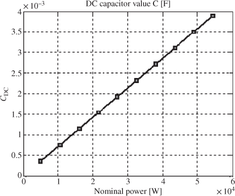
Figure 11.5 Value of the DC capacitor versus rated power up to 55 kW (Equation 11.4)
11.1.4 Flying Capacitor Rating
FC capacitance, assuming sinusoidal converter output voltages and currents, can be calculated as [21]:
where ![]() is the RMS phase current flowing through the FC,
is the RMS phase current flowing through the FC, ![]() is the assumed maximum voltage ripple across the FC and
is the assumed maximum voltage ripple across the FC and ![]() is the frequency of changes of the switching states (charging and discharging) applied to the FCC, which are used for FC balancing. It is important to note that
is the frequency of changes of the switching states (charging and discharging) applied to the FCC, which are used for FC balancing. It is important to note that ![]() is not the same as the switching frequency, because the frequency of changes of the switching states applied to FCC depends on the type of modulation and, in the case of FC balancing, is typically a multiple of the switching frequency by a factor 0.5, 1 or 2.
is not the same as the switching frequency, because the frequency of changes of the switching states applied to FCC depends on the type of modulation and, in the case of FC balancing, is typically a multiple of the switching frequency by a factor 0.5, 1 or 2.
11.1.5 L and LCL Filter Rating
An AC–DC–AC converter is connected to the grid through an AC filter (e.g., L or LCL). The inductance allows current control by the voltage drop on itself. In order to obtain better reduction of current ripples, the LCL T-type filter has been introduced.
For the LCL filter to fulfill the grid codes, or recommended practices for example, IEEE 519-1992 [21 22] a variety of optimization criteria exist, such as minimum costs, losses, volume, weight, or design. However, it is a complex task because many parameters influence this process, for example, DC-link voltage level, phase current, modulation method, modulation index, switching frequency, fundamental frequency, and resonance frequency. Therefore, the design can be done using two different methods:
- simple trial-and-error method, which has to be supported by simulation to prove that the grid codes are fulfilled (simulation has to take into account all elements of the system),
- complicated iterative, which calculates directly the filter parameters fulfilling the grid code; however, detailed information is required regarding many parameters, for example, modulation method and modulation index [24 25].
A general algorithm of a simple trial-and-error filter design is presented in Figure 11.6. The starting point for the design procedure is usually assumptions of the converter's rated power, grid, and switching frequencies. Those parameters allow the calculation of base values (base impedance ![]() , capacitance
, capacitance ![]() and inductance
and inductance ![]() ):
):
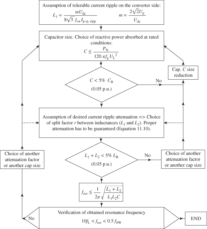
Figure 11.6 General design algorithm of low-pass LCL filter where  is the converter-side inductance,
  is the grid-side inductance LCL filter,
  is the converter RMS voltage, and
  is the peak-to-peak ripple current
where ![]() is the line-to-line grid voltage and
is the line-to-line grid voltage and ![]() is the grid voltage pulsation.
is the grid voltage pulsation.
The first step is the design of the filter inductance. This should be designed carefully because a large inductance value may, by itself, attenuate higher frequencies and limit current ripples. On the other hand, it brings many disadvantages, such as greater inductor size, a decrease in the converter's dynamics and a smaller range of operation. The operation range is limited through the maximum reachable voltage drop across the inductance. It is dependent indirectly on the DC-link voltage. Thus, in order to achieve a large current through the inductance, a high DC-link voltage level or low input inductance is needed.
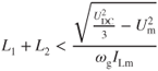
The maximum total inductance of the input LCL filter may not be larger than [14]:
where ![]() is the grid maximum voltage value and
is the grid maximum voltage value and ![]() is the grid current maximum value.
is the grid current maximum value.
In addition, the total value of the LCL filter inductance should be lower than 5% of the base impedance value, in order to limit the voltage drop during normal operation and to achieve excellent dynamics and reasonable cost [14 26]. Based on the IEEE 519-1992 limitations and the assumption that peak ripples must not exceed 10% of the grid current, the converter-side inductance ![]() can be calculated, as shown in Figure 11.6 [14 23]. Typically, the converter-side inductance
can be calculated, as shown in Figure 11.6 [14 23]. Typically, the converter-side inductance ![]() is larger than the grid-side inductance
is larger than the grid-side inductance ![]() in order to attenuate most of the current ripple. In this case, a split factor
in order to attenuate most of the current ripple. In this case, a split factor ![]() , given by Liserre et al. [26]:
, given by Liserre et al. [26]:
is set by the desirable ripple attenuation described as:
where ![]() is the grid higher harmonics current and
is the grid higher harmonics current and ![]() is the converter higher harmonics current.
is the converter higher harmonics current.
In order to limit the harmonic currents absorbed by the filter, the capacitor is limited to 5% of the reactive power absorbed at rated conditions (base capacitance) [26]. Therefore, the final capacitance of the LCL filter (Y-connected) cannot be larger than as presented in Figure 11.6. In the case of just an ![]() filter, the value of the inductance can equal
filter, the value of the inductance can equal ![]() .
.
Another constraint in the design process of the LCL filter is an obligation to maintain the resonance frequency ![]() between 10 times the line frequency
between 10 times the line frequency ![]() and one-half of the switching frequency
and one-half of the switching frequency ![]() [14 26]. These limits guarantee that there will be no resonance problems in both the lower and higher parts of the harmonic spectrum. The actual resonance frequency of the LCL filter may be calculated as in Figure 11.6.
[14 26]. These limits guarantee that there will be no resonance problems in both the lower and higher parts of the harmonic spectrum. The actual resonance frequency of the LCL filter may be calculated as in Figure 11.6.
11.1.6 Comparison
Table 11.1 presents a comparison of selected classical AC–DC–AC converter topologies: two-level three-phase/three-phase converter (2L-3/3); three-level three-phase/three-phase DCC converter (3L-DCC-3/3); three-level three-phase/three-phase FCC converter (3L-FCC-3/3), and simplified topologies with reduced number of transistors: simplified AC–DC–AC two-level converter three-phase/one-phase (S2L-3/1), and three-phase/three-phase (S2L-3/3); simplified DCC AC–DC–AC converter three-phase/one-phase (S3L-DCC 3/1), and three-phase/three-phase (S3L-DCC 3/3).
Table 11.1 Comparison of selected AC–DC–AC converter topologies
| I | II | III | IV | V | VI | VII | |
| 2L-3/3 | 12 | 0/1 | 1 | 1 | |||
| S2L-3/3 | 8 | 0/2 | |||||
| S2L-3/1 | 6 | 0/2 | |||||
| 3L-DCC-3/3 | 24 | 12/2 | 1 | ||||
| S3L-DCC 3/3 | 16 | 8/2 | |||||
| S3L-DCC 3/1 | 12 | 6/2 | |||||
| 3L-FCC-3/3 | 24 | 0/7b |
aSimplified converter only between transistors legs.
bIncluding one standard electrolytic capacitor in DC link and six floating capacitors designed for rapid discharging.
I, Total number of IGBT transistors; II, Number of independent diodes/number of capacitors; III, Total number of converter states; IV, DC voltage level in p.u. in comparison to 2L-3/3; V, Blocking voltage for transistors in p.u. in comparison to 2L-3/3; VI, Minimum voltage level step change; VII, total L filter inductance for all phases.
11.2 Pulse-Width Modulation for AC–DC–AC Topologies
Pulse-width modulation (PWM) for AC–DC–AC converters can be divided into two groups, depending on the single-phase or three-phase topology of the converter. The space vector modulation (SVM) techniques for the different topologies of classical single-phase H-bridge AC–DC VSCs have been presented in Chapter 23. In this section, only the SVM techniques for the following are presented:
- classical three-phase two-level converter
- classical three-phase three-level converters: DCC and FCC
- simplified single-phase and three-phase two-level converter
- simplified single-phase and three-phase three-level DCC
Modulation techniques for VSCs are responsible for the generation of average output voltage (represented by different widths of short voltage pulses) equal to reference voltage with proper balancing of the additional DC voltage sources for multilevel converters. Depending on the VSC topologies and switching frequency, numerous PWM techniques can be listed [27 28]. Among them, two types of PWM are used most often: carrier-based PWM (CB-PWM) and SVM. However, recent advances and the constant development of digital signal processing systems (allowing high-precision digital implementation of complex control algorithms) has meant that SVM has gained a superior position in research and industry. The digital implementation of SVM is characterized by its simplicity. Furthermore, classical SVM with symmetrical switching placement is equivalent to CB-PWM with an additional ![]() peak amplitude triangular zero sequence signal (ZSS) of the third harmonic frequency [29].
peak amplitude triangular zero sequence signal (ZSS) of the third harmonic frequency [29].
SVM is based on a single- or three-phase circuit representation in a stationary rectangular coordinate system using space vector (SV) theory. The reference SV ![]() is described by its length and its angle:
is described by its length and its angle:
where ![]() and
and ![]() are the
are the ![]() and
and ![]() components of
components of ![]() in a stationary rectangular coordinate system. To calculate the duration of the VSC switching states, a value of the modulation index is indispensable, which is proportional to the SV length with respect to the DC-link voltage. Usually,
in a stationary rectangular coordinate system. To calculate the duration of the VSC switching states, a value of the modulation index is indispensable, which is proportional to the SV length with respect to the DC-link voltage. Usually, ![]() is defined as:
is defined as:
where ![]() denotes the number of VSC output phase voltage levels. The allowable length of vector
denotes the number of VSC output phase voltage levels. The allowable length of vector ![]() for each
for each ![]() angle in the linear operation range is given by
angle in the linear operation range is given by ![]() . Therefore, the linear modulation range of an
. Therefore, the linear modulation range of an ![]() -level VSC is limited to:
-level VSC is limited to:
which is the maximal converter linear range of operation [30].
Table 11.2 Switching states for single leg of the two-level VSC
| States | ||
| OFF | ||
| ON |
11.2.1 Space Vector Modulation for Classical Three-Phase Two-Level Converter
Table 11.2 presents all possible switching states for a single leg of a two-level VSC (see Figure 11.2(a), generating output pole voltage ![]() between the phase terminal
between the phase terminal ![]() and the DC-link “
and the DC-link “![]() ” terminal
” terminal ![]() , where
, where ![]() is the leg indicator.
is the leg indicator.
Because the three-phase system is assumed symmetric, the Clarke transformation from natural ![]() into a stationary
into a stationary ![]() coordinate system can be used. Figure 11.7(a) shows a graphical representation of the SV
coordinate system can be used. Figure 11.7(a) shows a graphical representation of the SV ![]() voltage plane with possible output voltage vectors of the three-phase two-level converter. All voltage vectors are described by three numbers, which correspond to the switching states in leg
voltage plane with possible output voltage vectors of the three-phase two-level converter. All voltage vectors are described by three numbers, which correspond to the switching states in leg ![]() , leg
, leg ![]() , and leg
, and leg ![]() , respectively. A three-phase two-level converter provides eight possible switching states, comprising six active (
, respectively. A three-phase two-level converter provides eight possible switching states, comprising six active (![]() ,
, ![]() ,
, ![]() ,
, ![]() ,
, ![]() , and
, and ![]() ) and two zero switching states (
) and two zero switching states (![]() and
and ![]() ). The active vectors divide the plane into six sectors, where reference vector
). The active vectors divide the plane into six sectors, where reference vector ![]() is obtained by switching on (for proper time) two adjacent vectors. It can be seen that vector
is obtained by switching on (for proper time) two adjacent vectors. It can be seen that vector ![]() (see Figure 11.7(b)) can be implemented by the different ON/OFF switch sequences of
(see Figure 11.7(b)) can be implemented by the different ON/OFF switch sequences of ![]() and
and ![]() , and that zero vectors
, and that zero vectors ![]() and
and ![]() decrease the modulation index.
decrease the modulation index.
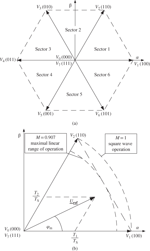
Figure 11.7 Space vector representation of three-phase two-level converter: (a) the  voltage plane and (b) sector 1 with representation of
Reference vector ![]() , used to solve equations that describe times
, used to solve equations that describe times ![]() ,
, ![]() ,
, ![]() , and
, and ![]() , is sampled with fixed sampling frequency
, is sampled with fixed sampling frequency ![]() . Digital implementation is described with the help of a simple trigonometric relationship for the first sector (11.14):
. Digital implementation is described with the help of a simple trigonometric relationship for the first sector (11.14):
and is recalculated for the following sectors (from 2 to 6). After the ![]() and
and ![]() calculation, the residual sampling time is reserved for zero vectors
calculation, the residual sampling time is reserved for zero vectors ![]() and
and ![]() with condition
with condition ![]() . Equation (11.14) is identical for all variants of SVM. The only difference is in the different placement of zero vectors
. Equation (11.14) is identical for all variants of SVM. The only difference is in the different placement of zero vectors ![]() and
and ![]() . This gives different equations defining
. This gives different equations defining ![]() and
and ![]() for each method, but the total duration time of the zero vectors must fulfill the following conditions:
for each method, but the total duration time of the zero vectors must fulfill the following conditions:
The most popular SVM method is modulation with symmetrical zero states' space vector PWM (SVPWM) where:
Figure 11.8 shows gate pulses for and the correlation between time ![]() ,
, ![]() , and the duration of vectors
, and the duration of vectors ![]() ,
, ![]() ,
, ![]() , and
, and ![]() . For the first sector, commutation delay can be computed as:
. For the first sector, commutation delay can be computed as:
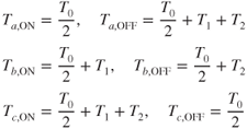
Figure 11.8 Vector placement in sampling time for three-phase SVM (SVPWM,  ) in sector 1
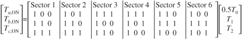
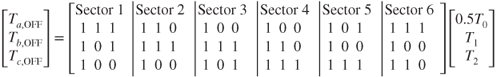
For classical SVM, times ![]() ,
, ![]() , and
, and ![]() are computed for one sector only. Commutation delay for the other sectors can be calculated with the help of a matrix:
are computed for one sector only. Commutation delay for the other sectors can be calculated with the help of a matrix:
11.2.2 Space Vector Modulation for Classical Three-Phase Three-Level Converter
Tables 11.3 and 11.4 present all possible switching states for the single leg of a three-level DCC and FCC (see Figure 11.2(b and c)), respectively, generating output pole voltage ![]() between the phase terminal
between the phase terminal ![]() and the DC-link “
and the DC-link “![]() ” terminal
” terminal ![]() , where
, where ![]() is the leg indicator.
is the leg indicator.
Table 11.3 Switching states for single leg of the three-level DCC
| States | |||
| OFF | OFF | ||
| OFF | ON | ||
| ON | ON |
Table 11.4 Switching states for single leg of the three-level FCC
| States | ||||
| OFF | OFF | |||
| A | ON | OFF | ||
| B | OFF | ON | ||
| ON | ON | |||
Figure 11.9 shows a graphical representation of the SV ![]() voltage plane with possible output voltage vectors of the three-phase three-level converter, which is constructed from the main switching states:
voltage plane with possible output voltage vectors of the three-phase three-level converter, which is constructed from the main switching states: ![]() ,
, ![]() , and
, and ![]() .
.
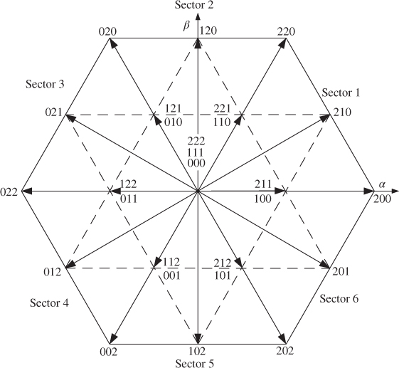
Figure 11.9 The  voltage plane for three-phase three-level converter
For the three-phase three-level VSC, the 27 voltage vectors can be specified as follows: three zero vectors (![]() ,
, ![]() , and
, and ![]() ); 12 internal small-amplitude vectors (
); 12 internal small-amplitude vectors (![]() ,
, ![]() ,
, ![]() ,
, ![]() ,
, ![]() ,
, ![]() ,
, ![]() ,
, ![]() ,
, ![]() ,
, ![]() ,
, ![]() , and
, and ![]() ); six middle medium-amplitude vectors (
); six middle medium-amplitude vectors (![]() ,
, ![]() ,
, ![]() ,
, ![]() ,
, ![]() , and
, and ![]() ); six external large-amplitude vectors (
); six external large-amplitude vectors (![]() ,
, ![]() ,
, ![]() ,
, ![]() ,
, ![]() , and
, and ![]() ).
).
The external vectors divide the vector plane into six sectors (see Figure 11.9), which is similar to the two-level VSC. However, for the three-level VSC, each sector is divided into four triangular regions. Figure 11.10(a and b) shows that the first sector is divided into four regions with all possible switching states for the DCC and the FCC topologies, respectively. As FCC switching state 1 can be divided into two redundant switching states: ![]() and
and ![]() (see Table 11.4, highlighted in Figure 11.10(b)), for this topology, the number of possible switching states increases to 64.
(see Table 11.4, highlighted in Figure 11.10(b)), for this topology, the number of possible switching states increases to 64.
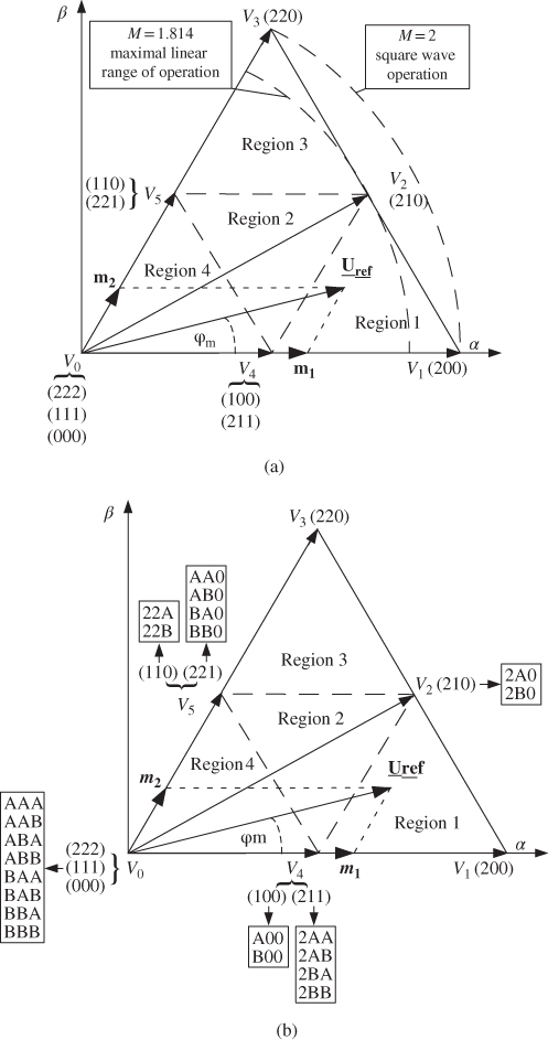
Figure 11.10 First sector with all possible switching states for (a) DCC and (b) FCC topologies
Conventional SVM for multilevel VSC is based on the assumption that for the generation of reference vector ![]() all possible nearest vectors, including their redundant states, are used (
all possible nearest vectors, including their redundant states, are used (![]() ,
, ![]() , and
, and ![]() in the first;
in the first; ![]() ,
, ![]() , and
, and ![]() in the second;
in the second; ![]() ,
, ![]() , and
, and ![]() in the third; and finally,
in the third; and finally, ![]() ,
, ![]() , and
, and ![]() in the fourth region) with symmetrical placement of the zero and internal vectors.
in the fourth region) with symmetrical placement of the zero and internal vectors.
The calculation of the region number of the location of the reference vector ![]() and switching times is based on two additional factors called the small modulation indices (
and switching times is based on two additional factors called the small modulation indices (![]() ,
, ![]() ). Index
). Index ![]() and
and ![]() are the projection of the reference vector on the sector sides, limited by the external vectors (see Figure 11.10). According to the trigonometric dependence, the small modulation indices are calculated as follows:
are the projection of the reference vector on the sector sides, limited by the external vectors (see Figure 11.10). According to the trigonometric dependence, the small modulation indices are calculated as follows:
In each sector, calculations are carried out to achieve vector switching times that are the same and where the difference is only in the power switch selection for the gating signal. Thus, the reference vector is normalized to the first sector and after evaluation of the vector switching times, a proper transistor switching sequence is created for the reference position. Table 11.5 presents the calculation of the region number and switching times with respect to ![]() and
and ![]() .
.
Table 11.5 Calculation of region number and switching times
| Conditions | Region | Switching times |
| First | ||
| Second | ||
| Third | ||
| Fourth |
11.3 DC-Link Capacitors Voltage Balancing in Diode-Clamped Converter
Proper operation of the DCC requires that the voltage on each DC-link capacitor is stabilized on ½![]() . Unbalance in the DC-link gives inequality of redundant-internal vectors and distortions in middle vectors. In such cases, the generated voltage is different from the reference. In the DCC, the balancing of the DC-link capacitors depends on the switching states in all phases. When the phase is clamped to the neutral point of the DC-link (e.g., switching state 1 is chosen), it introduces additional current flowing from or to the neutral point. Consequently, inequalities occur in the charging and discharging of the DC-link capacitors. Other sources of imbalance in the capacitor voltages are asymmetries in the system:
. Unbalance in the DC-link gives inequality of redundant-internal vectors and distortions in middle vectors. In such cases, the generated voltage is different from the reference. In the DCC, the balancing of the DC-link capacitors depends on the switching states in all phases. When the phase is clamped to the neutral point of the DC-link (e.g., switching state 1 is chosen), it introduces additional current flowing from or to the neutral point. Consequently, inequalities occur in the charging and discharging of the DC-link capacitors. Other sources of imbalance in the capacitor voltages are asymmetries in the system:
- propagation of nonlinear IGBT gate signals (e.g., different IGBT ON/OFF times),
- equivalent series and parallel resistance of DC-link capacitors,
- differences in electrical parameters, such as each leg semiconductor devices and connection points.
It can be observed that selection of redundant-internal small-amplitude vectors always causes clamping of one or two phases to the neutral point of the DC-link. For example, when internal small-amplitude vector ![]() (redundant switching states
(redundant switching states ![]() and
and ![]() ) is chosen, this means that phase a is clamped to the neutral point of the DC-link for
) is chosen, this means that phase a is clamped to the neutral point of the DC-link for ![]() , and for the same time, phases a, b and c are clamped to the neutral point of the DC-link. Therefore, an additional controller (proportional or proportional-integral (PI)) can be introduced, which depending on the imbalance in the capacitors voltages will change the time division between the redundant-internal small-amplitude vectors. In this simple way, the balancing of the capacitor voltages will be ensured without increasing losses.
, and for the same time, phases a, b and c are clamped to the neutral point of the DC-link. Therefore, an additional controller (proportional or proportional-integral (PI)) can be introduced, which depending on the imbalance in the capacitors voltages will change the time division between the redundant-internal small-amplitude vectors. In this simple way, the balancing of the capacitor voltages will be ensured without increasing losses.
For proper balancing of DC-link voltages based on the additional controller, the information on the difference between the capacitor voltages is insufficient [31 32]. The second factor needed is the energy flow direction. The energy flow direction decides whether a selected redundant-internal small-amplitude vector will charge or discharge one of the DC-link capacitors. Therefore, the sign of the energy flow direction ![]() should be used to determine the sign of the additional controller input error between the DC-link capacitor voltages. If we assume that internal small-amplitude vector
should be used to determine the sign of the additional controller input error between the DC-link capacitor voltages. If we assume that internal small-amplitude vector ![]() is used to balance the DC-link voltages with a proportional controller, the ratio of
is used to balance the DC-link voltages with a proportional controller, the ratio of ![]() charging time division of
charging time division of ![]() (
(![]() ) and
) and ![]() (
(![]() ) is inversely proportional to the ratio of
) is inversely proportional to the ratio of ![]() and
and ![]() voltages with the sign of the energy flow direction
voltages with the sign of the energy flow direction ![]() :
:
where ![]() . Because of the sampling period, both of the DC-link capacitors during the calculated time
. Because of the sampling period, both of the DC-link capacitors during the calculated time ![]() will be charged or discharged. In the case of a PI controller in the aforementioned example, the ratio of
will be charged or discharged. In the case of a PI controller in the aforementioned example, the ratio of ![]() charging time division will be the controller output signal.
charging time division will be the controller output signal.
Determination of the energy flow direction ![]() in the case of machine-side VSC (MC) can be done by the determination of one of the following quantities [33]: instantaneous active power
in the case of machine-side VSC (MC) can be done by the determination of one of the following quantities [33]: instantaneous active power ![]() , electromagnetic torque
, electromagnetic torque ![]() , torque angle
, torque angle ![]() , or current vector to voltage vector angle
, or current vector to voltage vector angle ![]() . Choosing the appropriate quantity to use in the modulation algorithm depends on the purpose of the converter and the availability in the control. The active power consumed/produced by the MC can be estimated simply from the reference converter voltages
. Choosing the appropriate quantity to use in the modulation algorithm depends on the purpose of the converter and the availability in the control. The active power consumed/produced by the MC can be estimated simply from the reference converter voltages ![]() and
and ![]() (reconstructed from switching states) and the actual stator currents
(reconstructed from switching states) and the actual stator currents ![]() :
:
The sign of the power will define the operating mode of the converter: inverter or rectifier, that is, whether the energy is flowing from the capacitors to the motor, or vice versa. A similar procedure of calculation is used for electromagnetic torque ![]() , which is the result of the vector product of stator flux
, which is the result of the vector product of stator flux ![]() and the stator current
and the stator current ![]() component
component ![]() :
:
where ![]() is the number of pole pairs and
is the number of pole pairs and ![]() is the number of phases. In this case, the sign of the torque multiplied by mechanical speed
is the number of phases. In this case, the sign of the torque multiplied by mechanical speed ![]() shows the direction of energy flow. In the case of the torque angle
shows the direction of energy flow. In the case of the torque angle ![]() , no additional calculation is needed; only the sign of the
, no additional calculation is needed; only the sign of the ![]() is important. Therefore, current transformation to the
is important. Therefore, current transformation to the ![]() stator flux rotating frame and the sign of
stator flux rotating frame and the sign of ![]() current determines the direction of energy flow. Table 11.6 presents the final determination of the direction of energy flow in MC.
current determines the direction of energy flow. Table 11.6 presents the final determination of the direction of energy flow in MC.
Table 11.6 Determination of direction of energy flow in MC
| Parameter | Inverter (motoring) mode ( |
Rectifier (regenerating) mode ( |
Table 11.7 Determination of direction of energy flow in GC
| Parameter | Rectifier mode ( |
Inverter mode ( |
The determination of energy flow direction ![]() in grid-side VSC (GC) is similar and can be done by determination of one of the following quantities [33]: instantaneous active power
in grid-side VSC (GC) is similar and can be done by determination of one of the following quantities [33]: instantaneous active power ![]() , instantaneous active current
, instantaneous active current ![]() , or current vector to voltage vector angle
, or current vector to voltage vector angle ![]() . The active power consumed/produced by the grid-side converter can be estimated simply from the reference converter voltages
. The active power consumed/produced by the grid-side converter can be estimated simply from the reference converter voltages ![]() and
and ![]() and the actual line currents:
and the actual line currents:
Table 11.7 presents the final determination of the direction of energy flow in the line-side converter.
Figure 11.11 presents examples of switching sequences for the DCC in sector 1, assuming that the ratio of the time division of the internal small-amplitude vector is ![]() .
.
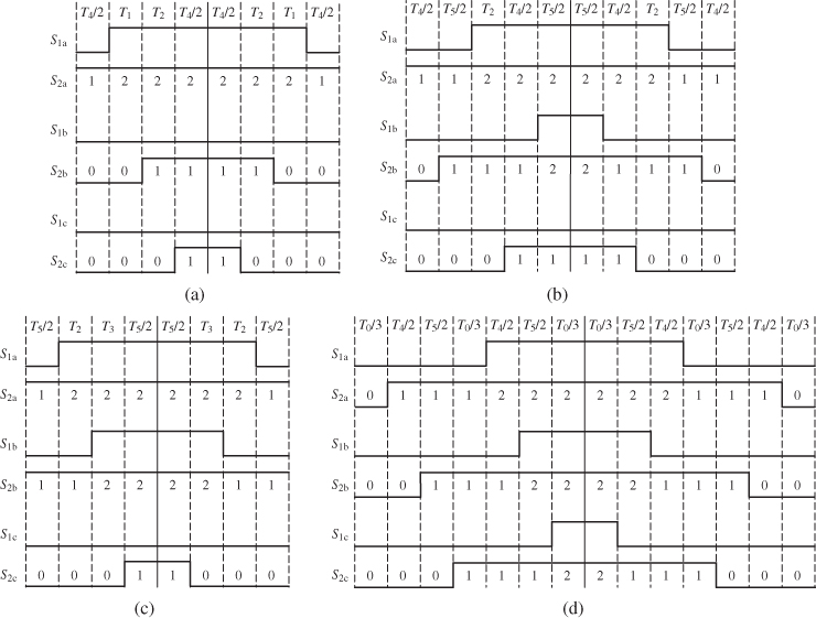
Figure 11.11 Switching sequence for DCC reference vector lying in (a) first, (b) second, (c) third, and (d) fourth regions in sector 1
11.3.1 Flying Capacitors Voltage Balancing in Flying Capacitor Converter
Proper operation of the FCC requires that the FC voltage ![]() should be half that of the DC-link voltage. With this condition, switching state 1 can be divided into two redundant states: 1A and 1B (highlighted in Table 11.4, Figure 11.10(b)), which generate the same output voltage
should be half that of the DC-link voltage. With this condition, switching state 1 can be divided into two redundant states: 1A and 1B (highlighted in Table 11.4, Figure 11.10(b)), which generate the same output voltage ![]() . As the output voltage does not depend on the type of selected state, either 1A or 1B can be used for independent control of
. As the output voltage does not depend on the type of selected state, either 1A or 1B can be used for independent control of ![]() . However, to decrease the number of commutations, only one state for each phase is chosen in the sampling period. For proper FC voltage balancing, only information about the sign of the phase current flowing through the FC is needed. Table 11.8 shows the selection between redundant states 1A or 1B based on the sign of phase current
. However, to decrease the number of commutations, only one state for each phase is chosen in the sampling period. For proper FC voltage balancing, only information about the sign of the phase current flowing through the FC is needed. Table 11.8 shows the selection between redundant states 1A or 1B based on the sign of phase current ![]() .
.
Table 11.8 Selection of redundant switching state for FC voltage balancing
| Conditions | ||
Figures 11.12 and 11.13 present the switching sequence in all regions in sector 1 for different switching states 1A or 1B for all phases, respectively. When the selected redundant state 1A or 1B is changed, the next modulation period can contain additional switching between sampling periods: two in the second and four in the first, third, and fourth regions. These additional switching can damage the converter; all switches are changing their state, which can generate overvoltage. To eliminate this phenomenon and to provide better switching distribution between particular switches, a modification of the switching pattern should be introduced [6] (see Figure 11.14).
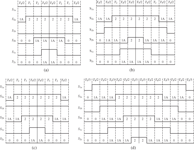
Figure 11.12 Switching sequence for FCC reference vector lying in (a) first, (b) second, (c) third, and (d) fourth regions in sector 1 for 1A state selection in each phase
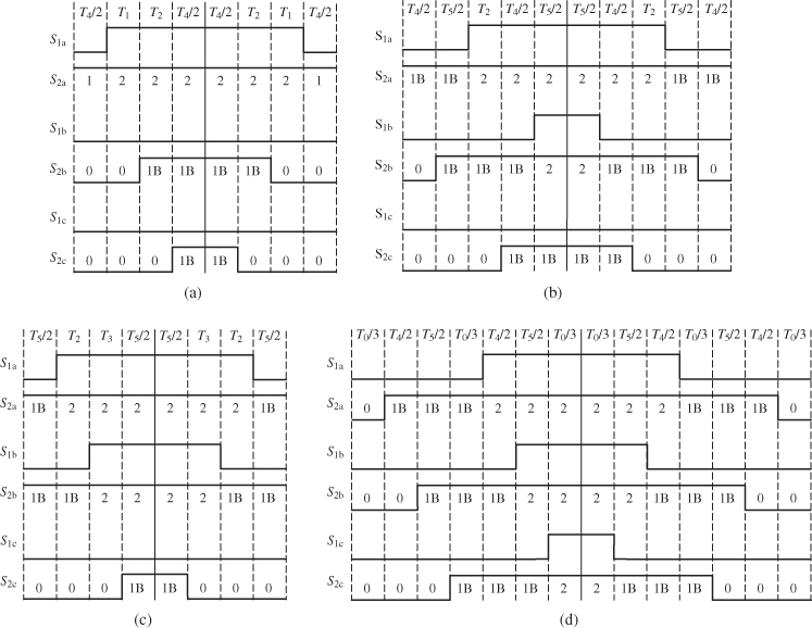
Figure 11.13 Switching sequence for FCC reference vector lying in (a) first, (b) second, (c) third, and (d) fourth region in sector 1 for 1B state selection in each phase
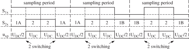
Figure 11.14 Modification of switching pattern in FCC
11.3.2 Pulse-Width Modulation for Simplified AC–DC–AC Topologies
Modulation for simplified AC–DC–AC converters is also realized separately for the DC–AC and AC–DC stages. It can be considered in this case as a single-phase modulation for the DC–AC part, as shown in Figures 11.3(a) and 11.4(a), or as three-phase modulation for the DC–AC or AC–DC parts, as shown in Figures 11.3(b) and 11.4(b).
Single-phase modulation for two-level DC–AC converters is simple and is described by Equation (11.25). Slightly more complicated is the modulation for a single-phase three-level DC–AC converter [13] shown in Figure 11.4(b), because an additional zero state is included (Figure 11.15).
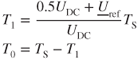
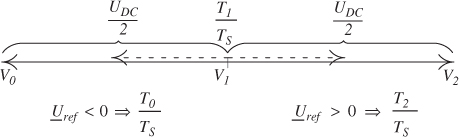
Figure 11.15 Vectors generated by 1DM technique DC/AC converter
It can be utilized using a universal concept of time-domain duty-cycle computation technique (11.26) for single-phase multilevel converters, described as a one-dimensional modulation (1DM) technique and presented in Ref. [34].
Modulation for a simplified three-phase converter requires a different approach than a classical topology, because only two reference signals in the ![]() coordinate system are needed to obtain a balanced three-phase voltage output, which implies that a higher voltage must be supplied to the DC-link to maintain the reference voltage vector in the linear modulation area (Figure 11.16).
coordinate system are needed to obtain a balanced three-phase voltage output, which implies that a higher voltage must be supplied to the DC-link to maintain the reference voltage vector in the linear modulation area (Figure 11.16).
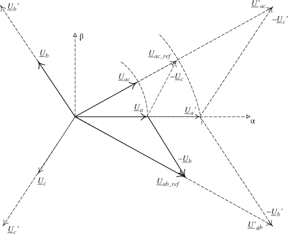
Figure 11.16 Generalized αβ voltage plane for three-phase simplified converters: imaginary vectors (dotted line),  , vectors achievable with standard DC-link voltage level,
  , vectors achievable with high DC voltage,
  , reference vectors
SVM for a simplified converter is based on a modified transformation from ![]() to
to ![]() [35]:
[35]:
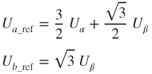
Figure 11.17 shows two cases of a graphical representation of a SV ![]() voltage plane with four achievable voltage vectors of the three-phase two-level simplified converter shown in Figure 11.3(b). In the first case (Figure 11.17(a)), all active vectors (
voltage plane with four achievable voltage vectors of the three-phase two-level simplified converter shown in Figure 11.3(b). In the first case (Figure 11.17(a)), all active vectors (![]() ,
, ![]() ,
, ![]() ,
, ![]() ) divide the
) divide the ![]() plane in four sectors: sector I (
plane in four sectors: sector I (![]() ), sector II (
), sector II (![]() ), sector III (
), sector III (![]() ), and finally, sector IV (
), and finally, sector IV (![]() ). The reference voltage vector
). The reference voltage vector ![]() , like in classical converters, could be obtained by switching two adjacent vectors, but this causes a voltage imbalance on DC-link capacitors. For the first sector, switching times can be computed as:
, like in classical converters, could be obtained by switching two adjacent vectors, but this causes a voltage imbalance on DC-link capacitors. For the first sector, switching times can be computed as:
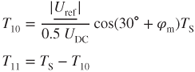
Figure 11.17 Space vector  (
( are defined in Table 11.2) representation of simplified three-phase two-level AC–DC–AC converter: (a) sector I
  and (b) sector I
The issue of voltage imbalance on DC-link capacitors can be solved by different divisions of the ![]() plane (Figure 11.17(b)). The number of sectors does not change, but the sectors are shifted 45° (e.g., sector I
plane (Figure 11.17(b)). The number of sectors does not change, but the sectors are shifted 45° (e.g., sector I ![]() ), which gives more vectors forming
), which gives more vectors forming ![]() (e.g.,
(e.g., ![]() in sector I). For the first sector, switching state times can be computed as [10]:
in sector I). For the first sector, switching state times can be computed as [10]:
Figure 11.18 Switching sequence for simplified two-level AC–DC–AC converter in each of four sectors
Switching signals for a simplified three-phase, 2-level AC–DC or DC–AC converter (Fig. 11.3(b)) are shown in Fig. 11.18.
Figure 11.19 Space vector  representation of three-phase three-level simplified converter
Another simplified three-phase converter is the three-level converter, as shown in Figure 11.4(b). A graphical representation of the nine achievable voltage vectors in the ![]() voltage plane for such a converter is shown in Figure 11.19.
voltage plane for such a converter is shown in Figure 11.19.
Eight of them (![]() ,
, ![]() ,
, ![]() ,
, ![]() ,
, ![]() ,
, ![]() ,
, ![]() ,
, ![]() ) are active and there is a zero vector (
) are active and there is a zero vector (![]() ). The reference voltage vector
). The reference voltage vector ![]() , like in classical converters, could be obtained by switching two adjacent vectors with the use of the zero voltage vector in the middle of the switching period [12]. Switching times for the sector I (
, like in classical converters, could be obtained by switching two adjacent vectors with the use of the zero voltage vector in the middle of the switching period [12]. Switching times for the sector I (![]() ) can be computed as:
) can be computed as:
and switching sequences for each of the eight sectors are shown in Figure 11.20.
Figure 11.20 Switching sequences for three-level simplified converter in each of the eight sectors
11.3.3 Compensation of Semiconductor Voltage Drop and Dead-Time Effect
The voltage drop on semiconductor devices and the dead-time (between pairs of IGBT's) value distorts the phase current. In both cases, it is the result of increased or decreased amplitude (length) ![]() of the reference SV, depending on the sign of the phase current, respectively. To avoid that, the voltage drop and the dead-time effect compensation algorithms are used. The impact of voltage drop and dead-time effect of semiconductor devices on phase current distortion have been well investigated for the classical two-level and multilevel converters. These methods can be divided into two groups:
of the reference SV, depending on the sign of the phase current, respectively. To avoid that, the voltage drop and the dead-time effect compensation algorithms are used. The impact of voltage drop and dead-time effect of semiconductor devices on phase current distortion have been well investigated for the classical two-level and multilevel converters. These methods can be divided into two groups:
- modification of amplitude (length)
 of the reference SV [6 36–38],
 - modification of the duty cycles at the output of the modulator [6 36, 38–40].
The solution is slightly more complicated in the case of simplified topologies. Because these converters use transistors in only two of three phases, the impact of voltage drop and dead-time effect of semiconductor devices is more significant, compared with that of classical topologies, owing to the different lengths of individual vectors. Moreover, these issues in reduced topologies cannot be considered as a mature. Therefore, in the following section, only reduced topologies will be considered.
Currents for ideal models of controlled switches and models including voltage drop on semiconductor devices are shown in Figure 11.21. In the other case, the converter currents are distorted significantly.
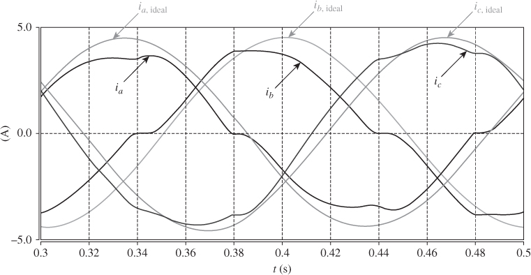
Figure 11.21 Ideal phase currents ( ,
,  ,
,  ) and phase currents including voltage drop on semiconductor devices (
 ,
,  ,
,  )
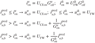
)
The effects of voltage drop on semiconductor devices are compensated by adding a correction to the reference signals on the input of the modulator [41]. In order to estimate the values of the voltage drops, the phase currents should be predicted for the next switching instant. Values of the predicted current in ![]() and
and ![]() phases are given by:
phases are given by:
where ![]() is the value of the current in the present sample and
is the value of the current in the present sample and ![]() is the value of the current in the earlier sample. Predicted current values are compared with values calculated from transistor and diode data sheets to determine the state of elements in both phases and corresponding voltage drops:
is the value of the current in the earlier sample. Predicted current values are compared with values calculated from transistor and diode data sheets to determine the state of elements in both phases and corresponding voltage drops:
where ![]() and
and ![]() are the currents for the transistor and diode, respectively.
are the currents for the transistor and diode, respectively. ![]() denotes the voltage drop on the transistor CE junction,
denotes the voltage drop on the transistor CE junction, ![]() denotes the voltage drop on the diode,
denotes the voltage drop on the diode, ![]() and
and ![]() are the conductances of the transistor and diode for conduction operation mode, respectively,
are the conductances of the transistor and diode for conduction operation mode, respectively, ![]() and
and ![]() are conductances of the transistor and diode for blocking operation mode, respectively, and finally,
are conductances of the transistor and diode for blocking operation mode, respectively, and finally, ![]() and
and ![]() are the resulting voltage drop for the transistor and diode, respectively.
are the resulting voltage drop for the transistor and diode, respectively.
Using ![]() and
and ![]() transformed to the two-phase coordinate system, as in Equation (11.27), a mean value of voltage drop per sampling period is estimated. Assuming that at switching state 1, the phase voltage error is
transformed to the two-phase coordinate system, as in Equation (11.27), a mean value of voltage drop per sampling period is estimated. Assuming that at switching state 1, the phase voltage error is ![]() (single transistor and a single DCC diode in a branch are conducting) and in the remaining states, it is
(single transistor and a single DCC diode in a branch are conducting) and in the remaining states, it is ![]() or
or ![]() we can write
we can write
the duty cycles for zero states. Therefore, the correcting signals for voltage drop compensation for a leg ![]() (and similar b leg
(and similar b leg ![]() ) are:
) are:
where ![]() denotes the direction of phase current flow,
denotes the direction of phase current flow, ![]() and
and ![]() are the duty cycles for positive and negative voltage output states and
are the duty cycles for positive and negative voltage output states and ![]() denotes zero voltage. These voltage-correcting signals are transformed to the
denotes zero voltage. These voltage-correcting signals are transformed to the ![]() coordinate system by using the modified transform from Equation (11.27) and adding them to the reference voltages for the modulator. Currents with no compensation and with the applied compensation method for semiconductor voltage drop only are shown in Figure 11.22.
coordinate system by using the modified transform from Equation (11.27) and adding them to the reference voltages for the modulator. Currents with no compensation and with the applied compensation method for semiconductor voltage drop only are shown in Figure 11.22.
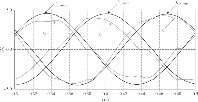
Figure 11.22 Phase currents without ( ,
,  ,
,  ) and with (
 ,
,  ,
,  ) voltage drop compensation
Another necessary compensation relates to the influence of the so-called dead time. Because IGBT devices turn off much more slowly than they turn on, there is a need for the introduction of a delay in control signals between complementary switching devices to prevent short-circuiting the DC-link. This effect is more visible for a low modulation index and low-frequency operation [41]. Figure 11.23 shows a comparison of phase currents without and with dead time included between complementary switching devices.
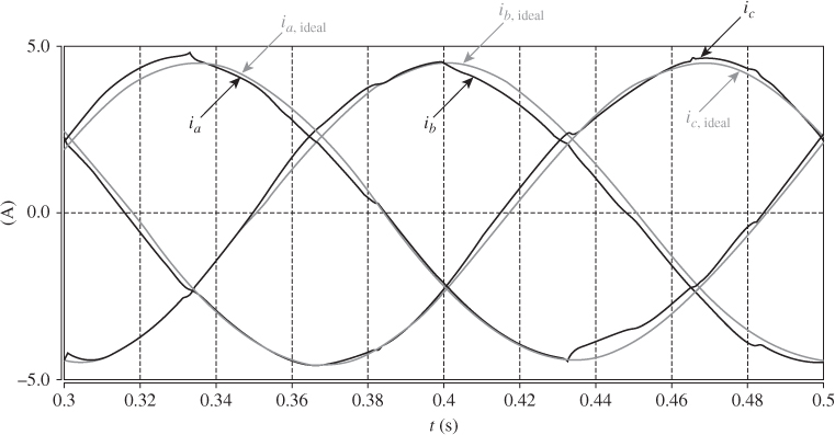
Figure 11.23 Phase currents without ( ,
,  ,
,  ) and with (
 ,
,  ,
,  ) dead time
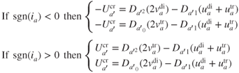
Correcting signals for limiting the effect of dead time ![]() are calculated based on current sign and saturation level
are calculated based on current sign and saturation level ![]() ; usually chosen experimentally to take into consideration the noise near the current zero-crossing. If phase current polarity, which depends on the measurement noise level as well as on the control delays, is not calculated properly, inadequate compensation can worsen the shape of the phase current. Therefore, in the range of
; usually chosen experimentally to take into consideration the noise near the current zero-crossing. If phase current polarity, which depends on the measurement noise level as well as on the control delays, is not calculated properly, inadequate compensation can worsen the shape of the phase current. Therefore, in the range of ![]() the dead-time correction value should be limited linearly. An example of a limiting function, modeled by two linear functions marked as 1 and 2, is shown in Figure 11.24.
the dead-time correction value should be limited linearly. An example of a limiting function, modeled by two linear functions marked as 1 and 2, is shown in Figure 11.24.
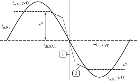
Figure 11.24 Phase current and correction function for dead-time compensation
Because a reduced converter generates voltages that are not equal in length in vector representation (Figure 11.19), after obtaining the above correction, it is necessary to choose which switching combination should not only be increased or decreased, but also multiplied with a scaling constant. For long vectors (![]() and
and ![]() for the two-level converter and
for the two-level converter and ![]() and
and ![]() for the three-level converter), the scaling constant is equal to
for the three-level converter), the scaling constant is equal to ![]() , but for short vectors (
, but for short vectors (![]() and
and ![]() for two-level converter
for two-level converter ![]() ,
, ![]() ,
, ![]() ,
, ![]() ,
, ![]() , and
, and ![]() for three-level converter), the scaling constant is equal to
for three-level converter), the scaling constant is equal to ![]() . The effect of compensation for converters without and with dead-time compensation between the complementary switching devices is shown in Figure 11.25. As can be seen, the shape of phase currents
. The effect of compensation for converters without and with dead-time compensation between the complementary switching devices is shown in Figure 11.25. As can be seen, the shape of phase currents ![]() and
and ![]() is improved mainly near the zero-crossing.
is improved mainly near the zero-crossing.
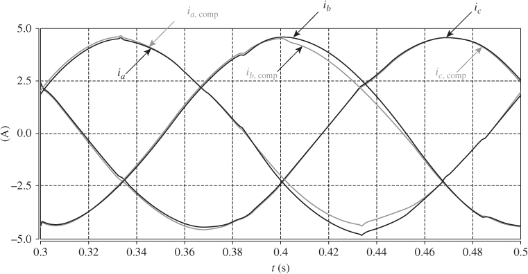
Figure 11.25 Phase currents without ( ,
,  ,
,  ) and with (
 ,
,  ,
,  ) dead-time compensation between complementary switching devices
11.4 Control Algorithms for AC–DC–AC Converters
A typical application of an AC–DC–AC converter is the interconnection of an electrical machine (motor/generator) with the grid. In this case, advanced control methods should be used to obtain high power quality for the grid-side converter (GC) and good energy utilization for the machine-side converter (MC). Control of both converters can be considered as a dual problem (Figure 11.26) [42–44]. We can distinguish among the most popular control methods voltage-oriented control (VOC) and direct power control-space vector modulation (DPC-SVM) for the GC, as well as field-oriented control (FOC) and direct torque control-space vector modulation (DTC-SVM) for the MC. All these methods are very well described in the literature [42–50]. This section presents the theoretical background of selected control methods and gives basic information regarding the design of the controllers.
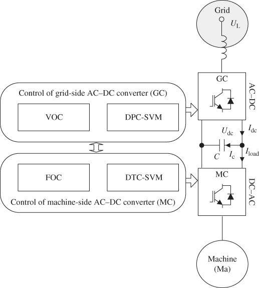
Figure 11.26 Space vector control methods for grid-side converter (GC) and machine-side converter (MC) in an AC–DC–AC indirect converter
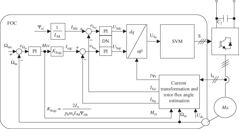
Figure 11.27 Indirect field-oriented control (IFOC), where  is the commanded rotor flux
11.4.1 Field-Oriented Control of an AC–DC Machine-Side Converter
The FOC can be divided into direct field-oriented control (DFOC) and indirect field-oriented control (IFOC). A simplified block diagram of the IFOC is presented in Figure 11.27. The IFOC seems to be more convenient than DFOC, especially for permanent magnet synchronous machines (PMSMs) because flux estimation is not necessary. The IFOC needs the coordinate system to rotate synchronously with the rotor flux angular speed ![]() . In this case, the system of coordinates is oriented with the
. In this case, the system of coordinates is oriented with the ![]() rotor flux linkage component, such that:
rotor flux linkage component, such that:
All variables are transformed from the natural ![]() into rotating the
into rotating the ![]() reference frame. Then, the referenced stator current values
reference frame. Then, the referenced stator current values ![]() and
and ![]() are compared with the actual values of stator current component
are compared with the actual values of stator current component ![]() and
and ![]() , respectively. It should be stressed that (for steady state)
, respectively. It should be stressed that (for steady state) ![]() is equal to the magnetizing current, whereas the torque state, both dynamic and steady, is proportional to
is equal to the magnetizing current, whereas the torque state, both dynamic and steady, is proportional to ![]() . The current errors
. The current errors ![]() and
and ![]() are fed to two PI controllers, which generate referenced stator voltage components
are fed to two PI controllers, which generate referenced stator voltage components ![]() and
and ![]() , respectively. Furthermore, referenced voltages are transformed from rotating
, respectively. Furthermore, referenced voltages are transformed from rotating ![]() coordinates into the stationary
coordinates into the stationary ![]() coordinates system by using the rotor flux vector position angle
coordinates system by using the rotor flux vector position angle ![]() . Therefore, the obtained referenced voltage vector
. Therefore, the obtained referenced voltage vector ![]() is delivered to SVM, which generates the appropriate switching signals
is delivered to SVM, which generates the appropriate switching signals ![]() .
.
It should be taken into account that ![]() and
and ![]() are coupled with each other. Any change of
are coupled with each other. Any change of ![]() stator voltage component has an influence not only for d but also for the q current component (the same applies to the q component). Therefore, a decoupling network (DN) in the control loops is necessary. The solution for this phenomenon is presented in Figure 11.28. It should be noted that the decoupling between the d and q axes appears in all control methods, discussed in this chapter, for both GCs and MCs (VOC and FOC). In the case of direct torque control and direct power control, the SV modulated by the coupling phenomenon is reduced significantly and therefore, DN can be omitted.
stator voltage component has an influence not only for d but also for the q current component (the same applies to the q component). Therefore, a decoupling network (DN) in the control loops is necessary. The solution for this phenomenon is presented in Figure 11.28. It should be noted that the decoupling between the d and q axes appears in all control methods, discussed in this chapter, for both GCs and MCs (VOC and FOC). In the case of direct torque control and direct power control, the SV modulated by the coupling phenomenon is reduced significantly and therefore, DN can be omitted.
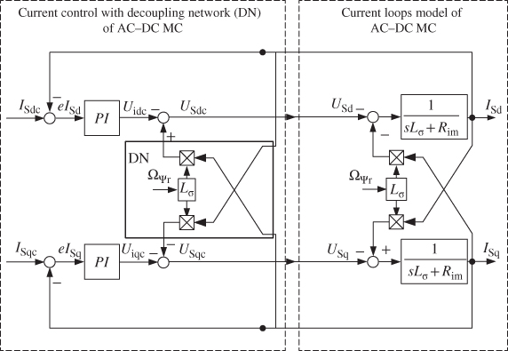
Figure 11.28 Current control with decoupling network (DN) for AC–DC converter, where  is the angular frequency of the AC system
11.4.2 Stator Current Controller Design
The model is very convenient to use for the synthesis and analysis of current controllers for MC. In the case of FOC, an asynchronous machine can be approximated and treated as a DC machine [48 51]. However, it should be pointed out that presence of coupling requires an application of a DN, as presented in Figure 11.28.
Hence, it can be seen that referenced decoupled machine converter voltages should be generated (after simplification) as follows:
where ![]() , and
, and ![]() ,
, ![]() is the total leakage factor,
is the total leakage factor, ![]() is the stator windings self-inductance, and
is the stator windings self-inductance, and ![]() are the stator and rotor windings resistances, respectively.
are the stator and rotor windings resistances, respectively.
It simplifies the analysis and enables the derivation of analytical expressions for the parameters of stator current controllers. The control structure will operate in a discontinuous domain (digital implementation); therefore, it is necessary to take into account the sampling period ![]() . This could be done by S&H block. Moreover, the statistical delay of the PWM in VSC
. This could be done by S&H block. Moreover, the statistical delay of the PWM in VSC ![]() should be taken into account. In the literature [6 16, 47 50, 51], the delay of the PWM is approximated from 0 to 2 sampling times
should be taken into account. In the literature [6 16, 47 50, 51], the delay of the PWM is approximated from 0 to 2 sampling times ![]() . Furthermore,
. Furthermore, ![]() is the VSC gain, and
is the VSC gain, and ![]() is the dead time of the VSC (
is the dead time of the VSC (![]() for an ideal converter). The block S&H and VSC sum of their time constants is expressed by:
for an ideal converter). The block S&H and VSC sum of their time constants is expressed by:
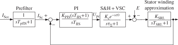
Figure 11.29 Stator current control loop approximation model where  is the referenced stator current before prefilter and
  is the prefilter time constant
Therefore, the model of the stator current control loop can be approximated as in Figure 11.29.
Please note that ![]() is the sum of small time constants,
is the sum of small time constants, ![]() is a large time constant, and
is a large time constant, and ![]() is a gain approximation of the stator windings. Hence,
is a gain approximation of the stator windings. Hence, ![]() gives a dominant pole. Among several methods of analysis, there are two simple ways for the design of the controller parameters: modulus optimum (MO) and symmetry optimum (SO) [48]. With the assumption that the internal voltage induced in the machine winding (EMF) is
gives a dominant pole. Among several methods of analysis, there are two simple ways for the design of the controller parameters: modulus optimum (MO) and symmetry optimum (SO) [48]. With the assumption that the internal voltage induced in the machine winding (EMF) is ![]() , for the circuit presented in Figure 11.29, the proportional gain and integral time constant of the PI current controller can be derived as [48 51]
, for the circuit presented in Figure 11.29, the proportional gain and integral time constant of the PI current controller can be derived as [48 51]
After simplifications, the closed-loop transfer function of the VSC can be approximated by the first-order transfer function as:
11.4.3 Direct Torque Control with Space Vector Modulation
To avoid the drawbacks of the switching table in classical DTC, instead of hysteresis controllers and the switching table, PI controllers with the SVM block have been introduced, as in IFOC. Therefore, DTC with SVM (DTC-SVM) joins DTC and IFOC features in one control structure, as shown in Figure 11.30.
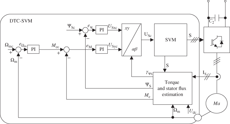
Figure 11.30 Direct torque control with space vector modulation (DTC-SVM) control for machine-side converter
DTC-SVM requires that the coordinate system rotates synchronously with the stator flux angular speed ![]() . In this case, the coordinate system is oriented with the
. In this case, the coordinate system is oriented with the ![]() stator flux linkage component, such that
stator flux linkage component, such that
Based on actual stator currents ![]() , DC voltage
, DC voltage ![]() , mechanical angular speed
, mechanical angular speed ![]() , and switching signals
, and switching signals ![]() , the commanded electromagnetic torque
, the commanded electromagnetic torque ![]() is delivered from the outer PI speed controller (Figure 11.30). Then,
is delivered from the outer PI speed controller (Figure 11.30). Then, ![]() and the commanded stator flux
and the commanded stator flux ![]() amplitudes are compared with the estimated values of electromagnetic torque
amplitudes are compared with the estimated values of electromagnetic torque ![]() and stator flux
and stator flux ![]() . The torque
. The torque ![]() and stator flux
and stator flux ![]() errors are fed to the PI controllers. The output signals are the referenced stator voltage components
errors are fed to the PI controllers. The output signals are the referenced stator voltage components ![]() and
and ![]() , respectively.
, respectively.
Furthermore, voltage components in the rotating ![]() system of coordinates are transformed into
system of coordinates are transformed into ![]() stationary coordinates by using
stationary coordinates by using ![]() stator flux position angle. The obtained referenced stator voltage SV
stator flux position angle. The obtained referenced stator voltage SV ![]() is delivered to the SVM, which generates the desired switching signals
is delivered to the SVM, which generates the desired switching signals ![]() for the MC.
for the MC.
11.4.4 Machine Stator Flux Controller Design
Figure 11.31 presents a block diagram of the PI-based stator flux magnitude control loop with neglected voltage drop on the stator resistance [47]. However, the ![]() delay introduced by the inverter is taken into consideration.
delay introduced by the inverter is taken into consideration.
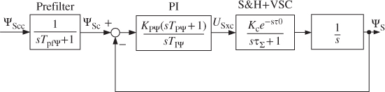
Figure 11.31 Block diagram of the stator flux magnitude control loop, where  is the referenced stator flux before prefilter and
  is the prefilter time constant, which equals the integral time constant of the flux PI controller
According to the SO criterion [48 49], the plant transfer function can be written as:
Therefore, according to the SO design technique, the stator flux PI controller parameters: proportional gain ![]() and the integral time constant
and the integral time constant ![]() can be calculated as [47 48]
can be calculated as [47 48]
11.4.5 Machine Electromagnetic Torque Controller Design
Figure 11.32 presents a block diagram of the simplified PI-based torque control loop with omitted coupling between the torque and stator flux. Consequently, the torque control loop is very simple Thus, for this model, not one criterion can be applied.
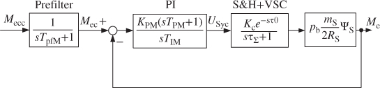
Figure 11.32 Block diagram of torque control loop, where  is the referenced electromagnetic torque before prefilter and
  is the prefilter time constant, which equals the integral time constant of the torque PI controller
In this case, according to Ref. [47], the simple (practical) way to design the torque PI controller can be used. Starting from initial values, for example, proportional gain ![]() and an integral time constant
and an integral time constant ![]() , the value of
, the value of ![]() increases cyclically. From these tests, the best value of
increases cyclically. From these tests, the best value of ![]() for fast torque response without oscillation and defined overshoot can be selected.
for fast torque response without oscillation and defined overshoot can be selected.
11.4.6 Machine Angular Speed Controller Design
If the magnitude of the stator flux is constant, ![]() , the dynamics of the IM can be described as follows:
, the dynamics of the IM can be described as follows:
where ![]() is the moment of inertia and
is the moment of inertia and ![]() is the load torque.
is the load torque.
Accordingly, Figure 11.33 shows a block diagram of the PI-based speed control loop, where ![]() is the transfer function of the closed torque control loop with prefilter (to compensate the forcing element in the transfer function of the closed torque control loop).
is the transfer function of the closed torque control loop with prefilter (to compensate the forcing element in the transfer function of the closed torque control loop).
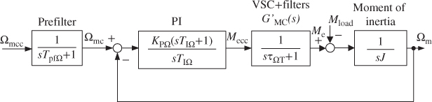
Figure 11.33 Block diagram of the speed control loop, where  is the referenced electromagnetic torque before prefilter and
  is the prefilter time constant, which equals the integral time constant of the speed PI controller
Approximating the torque control loop by the first-order integral part [47], the simplified ![]() transfer function can be written as:
transfer function can be written as:
where:
and:
where ![]() is the machine pole pairs number,
is the machine pole pairs number, ![]() is the phase number,
is the phase number, ![]() is the total leakage factor,
is the total leakage factor, ![]() is the stator windings self-inductance,
is the stator windings self-inductance, ![]() is the main magnetizing inductance,
is the main magnetizing inductance, ![]() is the rotor windings self-inductance, and
is the rotor windings self-inductance, and ![]() are the stator and rotor windings resistances, respectively.
are the stator and rotor windings resistances, respectively.
According to the SO criterion [48 49], the plant transfer function can be written as:
where ![]() is the gain of the plant and
is the gain of the plant and ![]() is the sum of small time constants and filters:
is the sum of small time constants and filters:
The speed PI controller parameters: proportional gain ![]() , and the integral time constant
, and the integral time constant ![]() , can be calculated as [47 48]
, can be calculated as [47 48]
11.4.7 Voltage-Oriented Control of an AC–DC Grid-Side Converter
The VOC presented in Figure 11.34 guarantees high dynamic and static performance via an internal current control loop. It has become very popular and, consequently, it has been developed and improved [15 53–55]. The goal of the control system is to maintain the DC-link voltage ![]() , at the required level, while currents drawn from the power system should be sinusoidal and in phase with the line voltage in order to satisfy the unity power factor (UPF) condition. The UPF condition is fulfilled when the line current vector
, at the required level, while currents drawn from the power system should be sinusoidal and in phase with the line voltage in order to satisfy the unity power factor (UPF) condition. The UPF condition is fulfilled when the line current vector ![]() is aligned with the phase voltage vector
is aligned with the phase voltage vector ![]() of the grid.
of the grid.
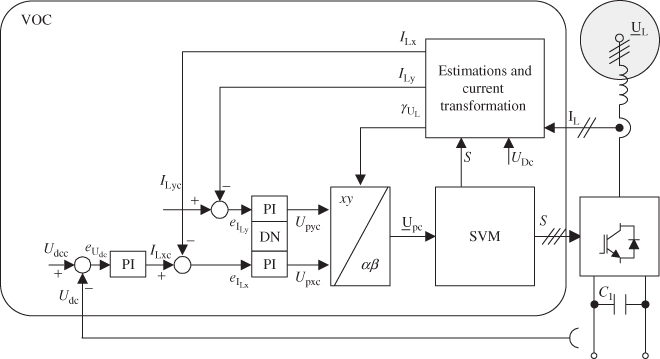
Figure 11.34 Voltage-oriented control (VOC)
For the UPF condition, the commanded value of the reactive component grid current vector ![]() is set to zero. The reference value of
is set to zero. The reference value of ![]() is an active component of the grid current vector. After comparing commanded currents with actual values, the errors are delivered to the PI current controllers. Voltages generated by the controllers are transformed to
is an active component of the grid current vector. After comparing commanded currents with actual values, the errors are delivered to the PI current controllers. Voltages generated by the controllers are transformed to ![]() coordinates by using the grid voltage vector position angle
coordinates by using the grid voltage vector position angle ![]() . Switching signals
. Switching signals ![]() for the GC are generated by an SVM.
for the GC are generated by an SVM.
11.4.8 Line Current Controllers of an AC–DC Grid-Side Converter
The model is very convenient to use for the synthesis and analysis of the current controllers for a grid-connected converter. However, the presence of coupling requires an application of a DN (as with FOC in Figure 11.28), as presented in Figure 11.35.
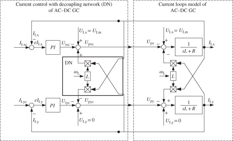
Figure 11.35 Current control with decoupling network (DN) for grid-side AC–DC converter
Hence, it can be seen clearly that referenced decoupled GC voltages should be generated as follows:
Therefore, the model of the current control loop can be presented as in Figure 11.36.
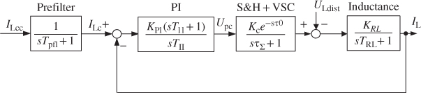
Figure 11.36 Current control loop model where  is the referenced grid current before prefilter and
  is the prefilter time constant, which equals the integral time constant of the current PI controller
Please note that ![]() is the sum of small time constants,
is the sum of small time constants, ![]() is a large time constant, and
is a large time constant, and ![]() is a gain of input choke. Hence,
is a gain of input choke. Hence, ![]() gives a dominant pole. Between several methods of analysis, there are two simple ways for the design of the controller parameters: MO and SO [48]. With the assumption that disturbance
gives a dominant pole. Between several methods of analysis, there are two simple ways for the design of the controller parameters: MO and SO [48]. With the assumption that disturbance ![]() for the circuit presented in Figure 11.5, the proportional gain and integral time constant of the PI current controller can be derived as [16]
for the circuit presented in Figure 11.5, the proportional gain and integral time constant of the PI current controller can be derived as [16]
After simplifications, the closed-loop transfer function of the VSC can be approximated by the first-order transfer function as:
For comparison, the parameters of the PI current controller calculated based on MO differ only in integral time constant:
The VSC with current controllers designed by MO can be approximated as:
For more information, please refer to Refs. [16 53].
11.4.9 Direct Power Control with Space Vector Modulation of an AC–DC Grid-Side Converter
Direct power control with space vector modulation (DPC-SVM) [52] assures high dynamic and static performance via internal power control loops. Instead of line currents, the active and reactive powers are used as control variables (Figure 11.37). The command active power ![]() is generated by the outer DC-link voltage controller, whereas command reactive power
is generated by the outer DC-link voltage controller, whereas command reactive power ![]() is set to zero for UPF operation. These values are compared with the estimated
is set to zero for UPF operation. These values are compared with the estimated ![]() and
and ![]() values, respectively [15 16]. Calculated errors
values, respectively [15 16]. Calculated errors ![]() and
and ![]() are delivered to the PI power controllers. Voltages generated by the power controllers are DC quantities, which eliminates steady-state error, as in VOC. Then, after transformation to stationary
are delivered to the PI power controllers. Voltages generated by the power controllers are DC quantities, which eliminates steady-state error, as in VOC. Then, after transformation to stationary ![]() coordinates [16], the voltages are used for the generation of switching signals in the SVM block.
coordinates [16], the voltages are used for the generation of switching signals in the SVM block.
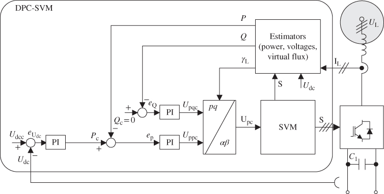
Figure 11.37 Direct power control with space vector modulation (DPC-SVM)
11.4.10 Line Power Controllers of an AC–DC Grid-Side Converter
The assumptions are the same as for the design of current controllers in VOC. Because the same block diagram can be applied to both ![]() and
and ![]() power controllers, only the active power
power controllers, only the active power ![]() control loop will be described briefly (Figure 11.38).
control loop will be described briefly (Figure 11.38).
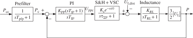
Figure 11.38 Power control loop with prefilter, where  is the referenced active power before prefilter,
  is the prefilter time constant, which equals the integral time constant of the power PI controller, and
  is the distortion of the grid voltage, for example, caused by higher harmonics
As in the case of VOC, SO is chosen because of its good response to a disturbance ![]() step change. With the assumption that
step change. With the assumption that ![]() , an open- and closed-loop transfer function can be obtained easily [16]. The proportional gain and integral time constant of the PI current controller in DPC-SVM can be calculated as:
, an open- and closed-loop transfer function can be obtained easily [16]. The proportional gain and integral time constant of the PI current controller in DPC-SVM can be calculated as:
The PI controller with such parameters gives power-tracking performance with approximately 40% overshoot. Therefore, for decreasing the overshoot, a first-order prefilter can be used on the reference signal:
where ![]() usually equals a few
usually equals a few ![]() [48].
[48].
In further investigation, a time delay of the prefilter is set to ![]() . Finally, a closed control loop of the VSC can be approximated by a first-order transfer function as:
. Finally, a closed control loop of the VSC can be approximated by a first-order transfer function as:
11.4.11 DC-Link Voltage Controller for an AC–DC Converter
For calculation of the parameters of a DC-link voltage controller, the inner current or power control loop can be modeled with the first-order transfer function [16]. Therefore, the power control loop of a grid-connected converter can be approximated by further consideration of the first-order block with an equivalent time constant ![]() as:
as:
where ![]() for inner current or power controllers designed by MO or
for inner current or power controllers designed by MO or ![]() for current/power controllers designed by SO criterion. Therefore, the DC-link voltage control loop can be modeled as in Figure 11.39.
for current/power controllers designed by SO criterion. Therefore, the DC-link voltage control loop can be modeled as in Figure 11.39.
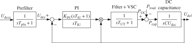
Figure 11.39 Block diagram for a simplified DC-link voltage control loop, where  is the referenced DC voltage before prefilter,
  is the DC voltage prefilter time constant, and
  is the grid-side converter active power
For the sake of simplicity, it can be assumed that
where ![]() is the DC voltage filter time constant,
is the DC voltage filter time constant, ![]() is a sum of time constants, and
is a sum of time constants, and ![]() is an equivalent integration time constant. Hence, the proportional gain
is an equivalent integration time constant. Hence, the proportional gain ![]() and integral time constant
and integral time constant ![]() of the DC-link voltage controller can be derived from
of the DC-link voltage controller can be derived from
11.5 AC–DC–AC Converter with Active Power FeedForward
If the accuracy of power matching of an AC–DC GC and DC–AC MC is improved, then a reduction of the DC capacitance is possible, but still providing the same quality of DC voltage stabilization. Because of DC voltage control that is more accurate, the lifetime of the DC capacitor will also be improved. When the DC current ![]() of a grid converter is equal to the DC current
of a grid converter is equal to the DC current ![]() of the MC, no current will flow through the DC capacitor C. As a result, the DC voltage will be well stabilized on a desired constant level.
of the MC, no current will flow through the DC capacitor C. As a result, the DC voltage will be well stabilized on a desired constant level.
However, despite the very good dynamic behaviors of the presented control methods, the control of the DC voltage could be improved [55–60]. Hence, APFF of the MC side to GC side has to be introduced. The idea of APFF is to give instantaneous power value from the AC MC side directly to the GC active power control loop, faster than the DC voltage feedback control loop. Because control of the power flow between the GC and MC is more precise, the stability of the DC-link voltage would increase significantly. Therefore, the value of the DC capacitance can be reduced significantly, if this is necessary. On the other hand, if the DC capacitance is required to be high for energy storage needs, the APFF can increase the lifetime of the capacitor significantly [57 58].
A simplified block diagram of the AC–DC–AC converter, which consists of a grid converter, machine converter, electrical machine, and APFF, is presented in Figure 11.40. It should be stressed here that in the case of operation with opposite direction power flow, when the MC control stabilizes the DC voltage and GC operates in inverting mode, the opposite direction of APFF is required, especially when standalone operation of GC is considered instead of stiff grid.
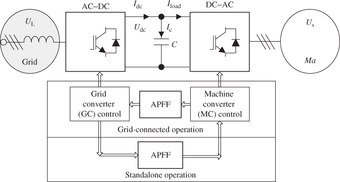
Figure 11.40 Simplified block diagram of the AC–DC–AC converter, which consists of an AC–DC and DC–AC converter, and APFF. Note: Direction of APFF changes in respect of grid-connected or standalone operation
Hereafter, the AC–DC–AC converter with APFF in control loops will be described. ![]() is equal to 0 in the case of the UPF operation. Under this condition, the GC input active power is derived by:
is equal to 0 in the case of the UPF operation. Under this condition, the GC input active power is derived by:
Within a steady-state condition ![]() and with the assumption that resistance of the input choke
and with the assumption that resistance of the input choke ![]() , from the machine side, the power consumed/produced by the MC is
, from the machine side, the power consumed/produced by the MC is
If virtual flux (VF) [15 16, 53 54] is adopted, it can be noticed that the active power of the GC is proportional to the virtual torque (VT) [16 45, 48]. Thanks to this, a convenient (as in the case of machines) equation for the active grid power calculation is derived:
where ![]() are the line current components in a rotating reference frame and
are the line current components in a rotating reference frame and ![]() are the grid VF components in a rotating reference frame.
are the grid VF components in a rotating reference frame.
On the MC, electromagnetic power can be approximated (neglecting power losses) as an active power delivered to the machine ![]() , so
, so
This is an insufficient assumption because of power losses ![]() in the real system; therefore, it should be written as
in the real system; therefore, it should be written as
Let us take into account stand still ![]() when nominal torque is applied. In such a case, the electromagnetic power will be 0, but the MC power
when nominal torque is applied. In such a case, the electromagnetic power will be 0, but the MC power ![]() will have a nonzero value. Estimation of this power is problematic because the parameters of the machine and power electronics devices are required. Hence, for simplicity of the control structure, a power estimator based on the commanded stator voltage
will have a nonzero value. Estimation of this power is problematic because the parameters of the machine and power electronics devices are required. Hence, for simplicity of the control structure, a power estimator based on the commanded stator voltage ![]() and actual stator current
and actual stator current ![]() will be taken into consideration:
will be taken into consideration:
11.5.1 Analysis of the Power Response Time Constant of an AC–DC–AC Converter
Based on Equation (11.58), the time constant of the GC response ![]() is determined. With the assumption that power losses of the converters can be neglected, the power-tracking performance can be expressed by
is determined. With the assumption that power losses of the converters can be neglected, the power-tracking performance can be expressed by
Similarly, for the MC, it can be written as
where ![]() is the equivalent time constant of the MC step response.
is the equivalent time constant of the MC step response.
11.5.2 Energy of the DC-Link Capacitor
The DC-link voltage can be described as
So,
Assuming the initial condition is in steady state, the actual DC-link voltage ![]() is equal to the commanded DC-link voltage
is equal to the commanded DC-link voltage ![]() . Therefore, Equation (11.78) can be rewritten as
. Therefore, Equation (11.78) can be rewritten as
where ![]() . Therefore, we can obtain
. Therefore, we can obtain
If the power losses of the GC and MC are neglected (for simplicity), the energy storage variation of the DC-link capacitor will be the integral of the difference between the GC power ![]() and the MC power
and the MC power ![]() . Therefore, it can be written as
. Therefore, it can be written as
From this equation, it can be concluded that for the most accurate control of the GC power ![]() , the commanded power
, the commanded power ![]() is
is
where ![]() describes the power of the DC-link voltage feedback control loop and
describes the power of the DC-link voltage feedback control loop and ![]() is equal to the instantaneous APFF signal. After the necessary assumptions, we obtain [16]:
is equal to the instantaneous APFF signal. After the necessary assumptions, we obtain [16]:
From Equations (11.75) and (11.76), the open-loop transfer function of the grid and machine converter active powers can be expressed as
Based on these equations, the analytic model of the AC–DC–AC converter with APFF can be defined, as in Figure 11.41. Such a system can be described by an open-loop transfer function as
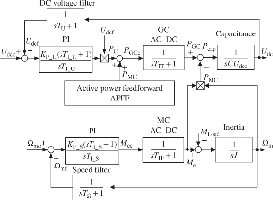
Figure 11.41 Simplified transmittances diagram of the AC–DC–AC converter with APFF
Assuming initial steady-state operation, ![]() and
and ![]() , the transfer function of the AC–DC–AC converter drive can be derived.
, the transfer function of the AC–DC–AC converter drive can be derived.
The active power of the machine converter can be calculated from the commanded values of the stator voltages and actual stator current. Assuming the case where ![]() , theoretically, the DC-link voltage should not be affected by the change of the load
, theoretically, the DC-link voltage should not be affected by the change of the load ![]() power. However, in the real system, the unbalanced power difference that causes the fluctuations of the DC-link voltage occurs mainly because of the power estimation error, the moment of inertia of the rotor and low-pass filter in the speed control loop, and the saturation of the commanded control variable.
power. However, in the real system, the unbalanced power difference that causes the fluctuations of the DC-link voltage occurs mainly because of the power estimation error, the moment of inertia of the rotor and low-pass filter in the speed control loop, and the saturation of the commanded control variable.
In Figure 11.42, waveforms illustrate the operation with a torque control loop. Torque reversal is applied when the mechanical speed reaches ±71% of the nominal speed. Very good stabilization of DC voltage can be seen with the use of APFF. The selected control method for the AC–DC–AC converter was direct power and torque control with space vector modulations (DPTC-SVM) [16]. The important advantage of this method is that there is no need to rescale the APFF signal.
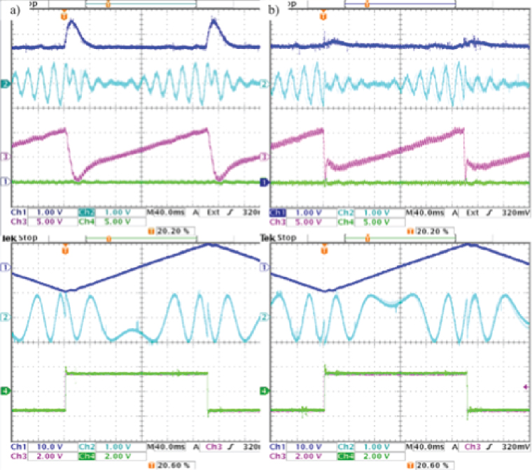
Figure 11.42 Torque reversal from −75% to 75% of nominal torque under DPTC-SVM: (a) only DC-link voltage feedback and (b) with APFF. From the top: DC-link voltage, grid current, active and reactive grid power, electrical machine mechanical speed, and stator current commanded and estimated electromagnetic torque
Moreover, based on Figure 11.42, it can be concluded that for ideal control methods with sufficiently high sampling time, the DC voltage fluctuation during transient for reduced capacitors could be even smaller than for the higher value of capacitance without APFF. Moreover, for the circuit with APFF, it can be seen that the fluctuations of DC voltage during transient for C = 1 p.u. and for C = 0.1 p.u. are almost equal for higher sampling times. Based on this, it can be stated that stabilization of the DC voltage in an AC–DC–AC converter with a controllable GC depends mainly on the quality (control loops accuracy and bandwidths) of the used DC voltage, the grid, and the MC power flow control methods. It can be expected that for high switching frequency, for example, ![]() 20 kHz, easily available for silicon carbide devices in wider power ranges than in the case of silicon devices, very accurate power flow control will be obtained. A simulation of DC voltage control accuracy in a simplified model (no switching losses) is presented as a function of sampling = switching frequency up to 100 kHz (Figure 11.43) with the DPTC-SVM control method applied [16].
20 kHz, easily available for silicon carbide devices in wider power ranges than in the case of silicon devices, very accurate power flow control will be obtained. A simulation of DC voltage control accuracy in a simplified model (no switching losses) is presented as a function of sampling = switching frequency up to 100 kHz (Figure 11.43) with the DPTC-SVM control method applied [16].
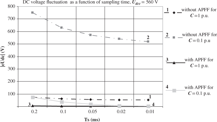
Figure 11.43 Module of the DC voltage fluctuation  as a function of sampling time
  , within transient in respect to load change from 0 to 1 p.u. with referenced DC voltage
  , and DPTC-SVM control method of the AC–DC–AC converter
11.6 Summary and Conclusions
This chapter has shown the different topologies of AC–DC–AC converters, which becoming increasingly popular in industrial applications, for example, wind turbines, smart grids, drives, and links connecting two electrical networks with different frequency or voltage levels. Among the presented configurations of AC–DC–AC converters, the simplified and classical two-level and multilevel converters are described and compared.
This chapter has also reviewed the modulation and control issues. Among the methods presented in this chapter, the FOC/VOC and DTC-SVM/DPC-SVM are described briefly. Selected issues relating to both the machine-side and grid-side, especially with APFF, have been discussed. Implemented APFFs have no negative impact on system performance in steady states, but do help to reduce DC capacitor and improve dynamic performance of the system. Selected laboratory and simulation tests with DPTC-SVM have been shown.
It is believed that owing to both continuing developments in power semiconductor components and to a reduction of their prices, as well as further elaboration of advanced control and modulation techniques, AC–DC–AC converters will have a significant impact on DPGSs.
References
- 1. Power Electronics Division TWERD (Polish: Zaklad Energoelektroniki TWERD) http://www.twerd.pl (accessed 18 December 2013).
- 2. ABB www.abb.com (accessed 18 December 2013).
- 3. Wu, B., Lang, Y. Zargari., et al. (2011) Power Conversion and control of Wind Energy Systems, John Wiley & Sons, Inc.
- 4. Kouro, S., Malinowski, M., Gopakumar, K. et al. (2010) Recent advances and industrial applications of multilevel converters. IEEE Transactions on Industrial Electronics, 57 (8), 2553–2580.
- 5. Friedli, T. (2010) Comparative evaluation of three-phase Si and SiC AC-AC converter systems comparative evaluation of three-phase Si and SiC AC-AC converter systems. PhD dissertation. ETH Zurich.
- 6. Styński, S. (2011) Analysis and control of multilevel AC–DC–AC flying capacitor converter fed from single–phase. PhD. thesis. Warsaw University of Technology, Warsaw, Poland.
- 7. Sędłak, M., Styński, S., Kaźmierkowski, M.P., and Malinowski, M. (2012) Three-level four-leg flying capacitor converter for renewable energy sources. Electrical Review, R.88 (12a), 6–11.
- 8. Enjeti, P. and Rahman, A. (1990) A new single phase to three phase converter with active input current shaping for low cost AC motor drives. Industry Applications Society Annual Meeting, 1990, Conference Record of the 1990 IEEE, October 7–12, 1990, Vol. 2, No. 4, pp. 935–942.
- 9. Jacobina, C.B., de Rossiter Correa, M.B., da Silva, E.R.C., and Lima, A.M.N. (1999) Induction motor drive system for low-power applications. IEEE Transactions on Industry Applications, 35 (1), 52–61.
- 10. Blaabjerg, F., Neacsu, D., and Pedersen, J. (1999) Adaptive SVM to compensate DC-link voltage ripple for four-switch three-phase voltage-source inverters. IEEE Transactions on Power Electronics, 14, 743–752.
- 11. Nabae, A., Takahashi, I., and Akagi, H. (1981) A new neutral-point-clamped PWM inverter. IEEE Transactions on Industry Applications, IA-17 (5), 518–523.
- 12. Bor-Ren, L. and Ta-Chang, W. (2004) Space vector modulation strategy for an eight-switch three-phase NPC converter. IEEE Transactions on Aerospace and Electronic Systems, 40 (2), 553–566.
- 13. Teodorescu, R., Liserre, M., and Rodríguez, P. (2011) Grid Converters for Photovoltaic and Wind Power Systems, John Wiley & Sons, Ltd-IEEE Press, p. 416.
- 14. Teichmann, R., Malinowski, M., and Bernet, S. (2005) Evaluation of three-level rectifiers for low-voltage utility applications. IEEE Transactions on Industrial Electronics, 52 (2), 471–481.
- 15. Malinowski, M. (2001) Sensorless control strategies for three–phase PWM rectifiers. PhD thesis. Warsaw University of Technology, Warsaw, Poland.
- 16. Jasinski, M. (2005) Direct power and torque control of AC–DC–AC converter–fed induction motor drives. PhD thesis. Warsaw University of Technology, Warsaw, Poland.
- 17. Carlsson, A. (1998) The back-to-back converter control and design. PhD thesis. Lund Institute of Technology, Lund.
- 18. Moran, L., Ziogas, P.D., and Joos, G. (1992) Design aspects of synchronous PWM rectifier-inverter systems under unbalanced input voltage conditions. IEEE Transactions on Industry Applications, 28 (6), 1286–1293.
- 19. Winkelnkemper, M. and Bernet, S. (2003) Design and optimalization of the DC-link capacitor of PWM voltage source inverter with active frontend for low-voltage drives. Proceedings of the EPE 2003 Conference.
- 20. Malesani, L., Rossetto, L., Tenti, P., and Tomasin, P. (1993) AC/DC/AC PWM converter with minimum energy storage in the dc link. Applied Power Electronics Conference and Exposition, 1993. APEC'93. Conference Proceedings 1993, Eighth Annual, March 7–11, 1993, pp. 306–311.
- 21. Fazel, S.S., Bernet, S., Krug, D., and Jalili, K. (2007) Design and comparison of 4-kV neutral-point-clamped, flying-capacitor, and series-connected H-bridge multilevel converters. IEEE Transactions on Industrial Electronics, 43 (4), 1032–1040.
- 22. IEEE Std 519–1992. (1993) IEEE Recommended Practices and Requirements for Harmonic Control in Electrical Power Systems.
- 23. Bernet, S., Ponnaluri, S., and Teichmann, R. (2002) Design and loss comparison of matrix converters and voltage source converters for modern ac-drives. Transactions of Industrial Electronics Society, Special Edition Matrix Converters.
- 24. Jalili, K. (2009) Investigation of control concepts for high-speed induction machine drives and grid side PWM voltage source converters. PhD thesis. Dresden University of Technology.
- 25. Jalili, K. and Bernet, S. (2009) Design of LCL filters of active-front-end two-level voltage-source converter. IEEE Transactions on Industrial Electronics, 56 (5), 1674–1689.
- 26. Liserre, M., Blaabjerg, F., and Hansen, S. (2001) Design and control of an LCL-filter based three-phase active rectifier. Industry Applications Conference, 2001. Thirty-Sixth IAS Annual Meeting. Conference Record of the 2001 IEEE, September 30–October 4, 2001, Vol. 1, pp. 299–307.
- 27. Holmes, D.G. and Lipo, T.A. (2003) Pulse Width Modulation for Power Converters, Principles and Practice, John Wiley & Sons, New York.
- 28. Rodriguez, J. (2005) Tutorial on multilevel converters. Proceedings of International Conference PELINCEC 2005, October 2005.
- 29. Holmes, D.G. (1996) The significance of zero space vector placement for carrier–based pwm schemes. IEEE Transactions on Industry Applications, 32 (5), 1122–1129.
- 30. Jenni, F. and Wueest, D. (1993) The optimization parameters of space vector modulation. Proceedings of EPE 1993, September 1993, pp. 376–381.
- 31. Marchesoni, M. and Tenca, P. (2002) Diode-clamped multilevel converters: a practicable way to balance DC-link voltages. IEEE Transactions on Industrial Electronics, 49 (4), 752–765.
- 32. Pou, J., Zaragoza, J., Ceballos, S. et al. (2007) Optimal voltage-balancing compensator in the modulation of a neutral-point-clamped converter. Proceedings of IEEE International Symposium on Industrial Electronics, June 2007, pp. 719–724.
- 33. Kolomyjski, W. (2009) Modulation strategies for three-level pwm converter-fed induction machine drives. PhD dissertation. Warsaw University of Technology, Warsaw, Poland.
- 34. Leon, J., Portillo, R., Vazquez, S. et al. (2008) Simple unified approach to develop a time-domain modulation strategy for single-phase multilevel converters. IEEE Transactions on Industrial Electronics, 55, 3239–3248.
- 35. Jacobina, C., da Silva, E., Lima, A., and Ribeiro, R. (1995) Vector and scalar control of a four switch three phase inverter. Industry Applications Conference, 1995. Thirtieth IAS Annual Meeting, IAS'95, Conference Record of the 1995 IEEE, Vol. 3, pp. 2422–2429.
- 36. Jeong, S.-G. and Park, M.–.H. (1991) The analysis and compensation of dead-time effects in pwm inverters. IEEE Transactions on Industrial Electronics, 38 (2), 108–114.
- 37. Ben-Brahim, L. (2004) On the compensation of dead time and zero-current crossing for a pwm–inverter–controlled ac servo drive. IEEE Transactions on Industrial Electronics, 51 (5), 1113–1118.
- 38. Dongsheng, Z. and Rouaud, D.G. (1999) Dead-time effect and compensations of three-level neutral point clamp inverters for high-performance drive applications. IEEE Transactions on Power Electronics, 14 (4), 782–788.
- 39. Leggate, D. and Kerkman, R.J. (1997) Pulse-based dead-time compensator for pwm voltage inverters. IEEE Transactions on Industrial Electronics, 44 (2), 191–197.
- 40. Oliveira, A.C., Jacobina, C.B., and Lima, A.M.N. (2007) Improved dead-time compensation for sinusoidal pwm inverters operating at high switching frequencies. IEEE Transactions on Industrial Electronics, 54 (4), 2295–2304.
- 41. Minshull, S.R., Bingham, C.M., Stone, D.A., and Foster, M.P. (2010) Compensation of nonlinearities in diode-clamped multilevel converters. IEEE Transactions on Industrial Electronics, 57, 2651–2658.
- 42. Kazmierkowski, M.P., Krishnan, R., and Blaabjerg, F. (2002) Control in Power Electronics, Academic Press, p. 579.
- 43. Wu, R., Dewan, S.B., and Slemon, G.R. (1990) A PWM AC-to-DC converter with fixed switching frequency. IEEE Transactions on Industry Applications, 26 (5), 880–885.
- 44. Zhou, D. and Rouaud, D. (1999) Regulation and design issues of a PWM three-phase rectifier. Proceedings of the 25th Annual Conference IECON'99, Vol. 1, pp. 485–489.
- 45. Manninen, V. (1995) Application of direct torque control modulation technology to a line converter. Proceedings of the EPE 1995 Conference, pp. 1.292–1.296.
- 46. Blaschke, F. (1971) A new method for the structural decoupling of A.C. induction machines. Proceedings of the Conference Record IFAC, Duesseldorf, Germany, October 1971, pp. 1–15.
- 47. Zelechowski, M. (2005) Space vector modulated-direct torque controlled (dtc-svm) inverter-fed induction motor drive. PhD dissertation. Warsaw University of Technology, Warsaw, Poland.
- 48. Kazmierkowski, M.P. and Tunia, H. (1994) Automatic Control of Converter–Fed Drives, Elsevier, Amsterdam, London, New York, Tokyo, PWN Warszawa.
- 49. Levine, W.S. (2000) Control System Fundamentals, CRC Press.
- 50. Liserre, M. (2001) Innovative control techniques of power converters for industrial automation. PhD thesis. Politecnico di Bari, Italy.
- 51. Blasko, V. and Kaura, V. (1997) A new mathematical model and control of a tree-phase AC-DC voltage source converter. IEEE Transactions on Power Electronics, 12 (1), 116–123.
- 52. Malinowski, M., Jasinski, M. and Kaźmierkowski, M.P. (2004) Simple Direct Power Control of Three-Phase PWM Rectifier Using Space-Vector Modulation (DPC-SVM). IEEE Transaction on Industrial Electronics, 51 (2), 447–454.
- 53. Wilamowski, B.M. and Irwin, J.D. (2011) The Industrial Electronics Handbook – Power Electronic and Motor Drives, 2nd edn, CRC Press, Boca Raton, FL, London, New York.
- 54. Chien, W.S. and Tzou, Y.-Y. (1998) Analysis and design on the reduction of DC-link electrolytic capacitor for AC/DC/AC converter applied to AC motor drives. Power Electronics Specialists Conference, 1998. PESC 98 Record. 29th Annual IEEE Volume 1, May 17–22, 1998, pp. 275–279.
- 55. Gu, B.G. and Nam, K. (2002) A DC-link capacitor minimization method through direct capacitor current control. Industry Applications Conference, 2002. 37th IAS Annual Meeting. Conference Record of the Volume 2, October 13–18, 2002, pp. 811–817.
- 56. Liao, J.C. and Yen, S.N. (2000) A novel instantaneous power control strategy and analytic model for integrated rectifier/inverter systems. IEEE Transactions on Power Electronics, 15 (6), 996–1006.
- 57. EPCOS (0000) Aluminium Electrolic Capacitors – Applications, DataSheet, www.epcos.com (accessed 18 December 2013).
- 58. EPCOS (0000) Aluminium Electrolic Capacitors – General Technical Information, DataSheet, www.epcos.com (accessed 18 December 2013).
- 59. Sobczuk, D.L. (1999) Application of ANN for control of PWM inverter fed induction motor drives. PhD thesis. Warsaw University of Technology, Warszawa.
- 60. Jasinski, M., Rafal, K., Bobrowska-Rafal, M., and Piasecki, S. (2011) Grid interfacing of distributed energy sources by three-level BtB NPC converter under distorted grid voltage. 2011 Workshop on Predictive Control of Electrical Drives and Power Electronics (PRECEDE), October 14–15, 2011, pp. 30–35.