
Chapter 23
Modulation and Control of Single-Phase Grid-Side Converters
Sebastian Styński and Mariusz Malinowski
Faculty of Electrical Engineering, Warsaw University of Technology, Warsaw, Poland
23.1 Introduction
Recent advances in the field of energy conversion (e.g., distributed power generation systems, traction and adjustable speed drives (ASD)) show a focus on voltage source converters (VSCs) [1–5]. VSCs are designed to meet the demands of high efficiency, robustness and low harmonics injection into power systems or low torque pulsation (corresponding to an increased motor lifetime due to decreased shaft vibrations). Expectations related to energy-saving and power quality solutions cause more frequent replacement of input diode rectifiers with active front end (AFE) because of the following main features [6]:
- Bidirectional power flow (allows regenerative breaking),
- Nearly sinusoidal input current with low harmonics distortion,
- High (including unity)-input power factor operation,
- Sufficient dynamics to follow load variation,
- Adjustment and stabilization of the DC-link voltage
 (distorted 100 Hz oscillation),
 - Operation under line voltage distortion (harmonics, sags, etc.).
Nowadays, AFE in AC–DC–AC energy conversion systems has started to be the standard solution. One of the important applications of medium-power AC–DC–AC fed ASD is high speed rail (HSR). Several different types of railway traction power systems (RTPSs) are used throughout the world [7 8]; however, in modern HSR, there is a trend toward using medium-voltage AC single-phase RTPSs. Therefore, issues related to the energy conversion for ASD used in the HSR become extremely important. In such systems, the VSCs connected to the grid through a step-down transformer are widely used as the AC–DC AFE.
Initially, as the AC–DC VSC in single-phase RTPS, an H-bridge converter (H-BC) fed from single low-voltage winding of the step-down transformer was used [8 9]. The H-BC provides three levels of converter output voltage ![]() :
: ![]() and
and ![]() . However, owing to the low converter-switching frequency for high power, the harmonics injected into the RTPS can be very high [9]. The current harmonics of the transformer high-voltage side generated by the VSC may have detrimental effects on the RTPS components and other loads, and is of great concern. Therefore, instead of a single H-BC, a parallel connected H-BC fed from two symmetrical low-voltage windings of the step-down transformer was introduced [10–14]. The main advantage of such a solution, due to the interleaved pulse-width modulation (PWM) between parallel connected H-BC modules, is the reduction in the current harmonics distortion of the transformer high-voltage side (five levels of converter output voltage on transformer high-voltage side is obtained:
. However, owing to the low converter-switching frequency for high power, the harmonics injected into the RTPS can be very high [9]. The current harmonics of the transformer high-voltage side generated by the VSC may have detrimental effects on the RTPS components and other loads, and is of great concern. Therefore, instead of a single H-BC, a parallel connected H-BC fed from two symmetrical low-voltage windings of the step-down transformer was introduced [10–14]. The main advantage of such a solution, due to the interleaved pulse-width modulation (PWM) between parallel connected H-BC modules, is the reduction in the current harmonics distortion of the transformer high-voltage side (five levels of converter output voltage on transformer high-voltage side is obtained: ![]() ,
, ![]() and
and ![]() ).
).
Recently, other multilevel VSC topologies have become attractive to medium-power conversion [15 16]. The idea of multilevel converters is based on a series connection of semiconductor devices with more than one DC voltage source. VSC operation above typical semiconductor voltage limits, with reduced voltage stress, lower common mode voltages, reduced harmonics distortion and lower filter requirements are some of the well-known advantages that have made this topology popular in both research and the industry. In particular, two multilevel topologies are widely used in ASD industrial applications: the diode clamped converter (DCC) and the flying capacitor converter (FCC). H-DCC was introduced into single-phase RTPS by Hitachi [17] in 1995 (Japan), and has received further attention over the years [18–21]. Despite many publications, the H-FCC has not been commercially applied to single-phase RTPS. Other multilevel cascade and hybrid topologies, which can be compared with classically used parallel-connected H-BC, have also been proposed [15], but they are not fully accepted by industry in transportation systems. A comparison between the multilevel H-DCC, H-FCC and parallel-connected H-BC – if the same voltage and current rating semiconductor devices are used – can be summarized as follows:
- the H-DCC and H-FCC input voltage and output DC-link voltage may be doubled, retaining the magnitude of input current constant,
- the H-DCC and H-FCC are fed from a single low-voltage winding with the same input current, as for the parallel connected H-BC but with doubled input voltage,
- the H-DCC uses additional semiconductor devices (clamping diodes),
- the H-FCC uses additional DC voltage sources (flying capacitors (FCs),
- a more complex PWM strategy is required for the H-DCC and H-FCC.
The choice between these topologies: H-DCC, H-FCC and parallel-connected H-BC, as well as choice of value of input voltage ![]() (especially for the H-DCC and H-FCC), depends not only on the technical requirements of the power circuit, such as the DC-link voltage. Equally important – if not more – are the economic requirements: the VSC and transformer volume, size and weight, component prices (semiconductor devices, especially) and so on. Therefore, it is not possible to clearly indicate the best VSC solution for HSR, and only a comparison for similar conditions can be made.
(especially for the H-DCC and H-FCC), depends not only on the technical requirements of the power circuit, such as the DC-link voltage. Equally important – if not more – are the economic requirements: the VSC and transformer volume, size and weight, component prices (semiconductor devices, especially) and so on. Therefore, it is not possible to clearly indicate the best VSC solution for HSR, and only a comparison for similar conditions can be made.
This chapter – divided into two main parts – is devoted to the modulation and control of single-phase grid-side converters in RTPS applications. The first part presents the analysis and comparative studies of PWM techniques with unipolar switching for the aforementioned converter topologies: the parallel-connected H-BC, the H-DCC and the H-FCC. Particular emphasis is placed on the impact of individual modulation techniques and topologies on the quality of the grid current and the harmonic content generated by the converter. The second part is devoted to the current control of single-phase VSC, where the basic structures of the ![]() synchronous reference frame are presented – proportional integral current control (PI-CC) and the
synchronous reference frame are presented – proportional integral current control (PI-CC) and the ![]() natural reference frame, proportional resonant current control (PR-CC). Moreover, the production of current and DC-link voltage controllers with tuning methods for PI and PR regulators is discussed. At the end, the active power feed forward (APFF) algorithm required to improve the dynamics of the DC-link stabilization (reduction of overvoltage in transient states) is provided.
natural reference frame, proportional resonant current control (PR-CC). Moreover, the production of current and DC-link voltage controllers with tuning methods for PI and PR regulators is discussed. At the end, the active power feed forward (APFF) algorithm required to improve the dynamics of the DC-link stabilization (reduction of overvoltage in transient states) is provided.
23.2 Modulation Techniques in Single-Phase Voltage Source Converters
The current harmonics generated by the VSC – as a result of the PWM strategy applied to VSC – are particularly important for single-phase RTPSs. The current harmonics distortion depends on the number of output voltage pattern-forming states visible from the transformer high-voltage side. The number of output voltage pattern-forming states is defined as follows: when one active and one zero switching state is applied symmetrically to the VSC, the output waveform will have three voltage-forming states arranged as follows: zero–active–zero. Therefore, a higher number of switching states applied to the VSC gives a lower current harmonics distortion. An increased number of output voltage pattern-forming states results in a decreasing input current ![]() distortion.
distortion.
Each VSC topology is characterized by a different method of output voltage pattern generation, dependent on the modulation technique applied. Moreover, each modulation technique can provide different numbers of output voltage pattern-forming states. Therefore, the comparison between modulation techniques for different topologies for single-phase RTPSs should be performed under strictly defined conditions. In this section, the following PWM techniques in the single-phase VSC are presented:
- hybrid pulse-width modulation (HPWM) and unipolar pulse-width modulation (UPWM) for parallel-connected H-BCs,
- one-dimensional nearest two vectors (1D-N2V) and one-dimensional nearest three vectors (1D-N3V) modulations for H-DCCs,
- 1D-N2V, 1D-N3V and one-dimensional nearest three with two redundant vectors (1D-N(3 + 2R)V) modulations for H-FCCs.
Taking into account the large number of PWM strategies and their possible modifications, the presentation will be based on the following assumptions:
- for each topology switching period,
 is the same,
 - each semiconductor device can only be switched two times (in ON–OFF–ON or OFF–ON–OFF sequences, where the switching is defined as an ON–OFF or OFF–ON state change) per period,
- for each modulation type, the minimum number of switching states is used in order to fulfill the modulation objectives.
Next, the comparison will be carried out for all VSC topologies and PWM techniques mentioned earlier. In order to perform the comparative study under similar conditions, for the control system the following assumptions have been made:
- transistors are ideal switches (switching losses are omitted),
- time delay between calculation and realization of transistor duty cycle is neglected,
- there is no dead time between pairs of transistors,
- grid voltage is
 is ideal sinusoidal,
 - transformer low-voltage side short circuit impedance is calculated as 25% of nominal impedance (typically between 20% and 30%),
- the charge of the DC-link capacitors
 and the FC is constant, regardless of grid voltage
  and DC-link voltage
  amplitude changes.
23.2.1 Parallel-Connected H-Bridge Converter (H-BC)
Figure 23.1 shows a single-phase parallel-connected H-BC with a common DC-link fed from the transformer with two low-voltage windings [10–14]. Among the main advantages of this topology are:
- low harmonics distortion of current
 for transformer high-voltage side at the hybrid and the unipolar modulations,
 - high reliability – in the case of one module failure, the H-BC still works with the same amplitude of
 but at twice reduced power and with an increased THD factor of
  .
.

Figure 23.1 Single-phase five-level parallel-connected H-bridge converter
Despite the obvious advantages introduced by parallel connection of the VSC, this is also a major disadvantage because of:
- the high cost, weight and size of a step-down transformer with two secondary windings,
- the increased current and voltage rating of the semiconductor devices.
Each module of the converter shown in Figure 23.1 has two legs, with insulated gate bipolar transistors (IGBTs) denoted ![]() and
and ![]() , where
, where ![]() is the negation of
is the negation of ![]() and
and ![]() is the leg indication:
is the leg indication: ![]() or
or ![]() . The IGBT is switched ON when the gate signal is
. The IGBT is switched ON when the gate signal is ![]() and switched OFF when the gate signal is
and switched OFF when the gate signal is ![]() . All switching states for one module are shown in Table 23.1.
. All switching states for one module are shown in Table 23.1.
Table 23.1 Switching states for single H-BC module
| Switch number | Levels of output t voltage |
|||
| 0 | 0 | 1 | 1 | |
| 1 | 0 | 1 | 0 | |
To calculate the duration of the switching states, the modulation index ![]() is indispensable, which is the proportion of the control algorithm reference
is indispensable, which is the proportion of the control algorithm reference ![]() with respect to the DC-link voltage
with respect to the DC-link voltage ![]() :
:
where ![]() is the reference amplitude of the converter output voltage. Note that
is the reference amplitude of the converter output voltage. Note that ![]() cannot be greater than
cannot be greater than ![]() ; thus,
; thus, ![]() .
.
The decision as to which output voltage level is applied (positive or negative) depends on ![]() (Equation 23.1):
(Equation 23.1):
The switching state time durations for every ![]() level are assigned as follows:
level are assigned as follows: ![]() for
for ![]() and
and ![]() for
for ![]() , and are calculated as:
, and are calculated as:
The IGBT state and its time duration depends on the PWM technique applied: the HPWM or UPWM.

Figure 23.2 Duty cycles for parallel-connected H-BC with hybrid modulation: (a) module 1, (b) module 2 and (c) parallel-connected H-BC  voltages with interleaved sampling periods ½
 between modules
The HPWM [22–24] for the single H-BC module is based on the assumption that only two among four transistors are pulse-width modulated in each sampling period (Figure 23.2). This means that in each period, only one leg is modulated and – as a consequence – only one of two possible redundant states for the ![]() voltage level is used. Switching states are applied symmetrically with respect to the middle of the sampling period. Which leg is modulated depends on the sign of
voltage level is used. Switching states are applied symmetrically with respect to the middle of the sampling period. Which leg is modulated depends on the sign of ![]() :
:
The HPWM applies two switching states in each sampling period for a single H-BC, which gives three output voltage ![]() forming states for module 1 (Figure 23.2(a)) and module 2 (Figure 23.2(b)). For two parallel-connected H-BC modules, the interleaved modulation is applied, which means that for each the same switching pattern and duty cycles of the HPWM can be used, but the sampling periods are shifted ½
forming states for module 1 (Figure 23.2(a)) and module 2 (Figure 23.2(b)). For two parallel-connected H-BC modules, the interleaved modulation is applied, which means that for each the same switching pattern and duty cycles of the HPWM can be used, but the sampling periods are shifted ½![]() between modules. Interleave modulation gives five levels on the transformer high-voltage side:
between modules. Interleave modulation gives five levels on the transformer high-voltage side: ![]() ,
, ![]() ,
, ![]() and five output voltage
and five output voltage ![]() forming states (Figure 23.2(c)).
forming states (Figure 23.2(c)).

Figure 23.3 Duty cycles for parallel-connected H-BC with unipolar modulation: (a) module 1, (b) module 2 and (c) parallel-connected H-BC  voltages with interleaved sampling periods ¼
 between modules
The other technique, UPWM [22 24], for the single H-BC module is based on the assumption that all switches are modulated in every sampling period (Figure 23.3). As a result, two redundant states for zero voltage level ![]() are applied. Thus, the UPWM applies three switching states in each sampling period for the single H-BC, which gives five output voltage
are applied. Thus, the UPWM applies three switching states in each sampling period for the single H-BC, which gives five output voltage ![]() forming states for module 1 (Figure 23.3(a)) and module 2 (Figure 23.3(b)). For the parallel-connected H-BC, interleaved modulation is applied, which means the same switching pattern and duty cycles of the UPWM can be used, but the sampling periods are shifted ¼
forming states for module 1 (Figure 23.3(a)) and module 2 (Figure 23.3(b)). For the parallel-connected H-BC, interleaved modulation is applied, which means the same switching pattern and duty cycles of the UPWM can be used, but the sampling periods are shifted ¼![]() between modules. Interleave modulation gives five levels on the transformer high-voltage side:
between modules. Interleave modulation gives five levels on the transformer high-voltage side: ![]() ,
, ![]() ,
, ![]() , and nine output voltage
, and nine output voltage ![]() forming states (Figure 23.3(c)).
forming states (Figure 23.3(c)).
23.2.2 H-Diode Clamped Converter (H-DCC)
The DCC was proposed in 1981 by Nabae et al. [25]. Figure 23.4 presents the single-phase H-DCC [18–21], which has two legs, with IGBTs denoted ![]() ,
, ![]() ,
, ![]() and
and ![]() , where
, where ![]() and
and ![]() are the negation of
are the negation of ![]() and
and ![]() , respectively and x is the leg indication: a or b. Two clamping diodes
, respectively and x is the leg indication: a or b. Two clamping diodes ![]() and
and ![]() are parallel connected to
are parallel connected to ![]() and
and ![]() for each leg, and the clamping point
for each leg, and the clamping point ![]() is connected to the center of the series capacitors
is connected to the center of the series capacitors ![]() and
and ![]() in the DC-link. Clamping diodes conduct the current during the generation of the intermediate H-DCC voltage levels.
in the DC-link. Clamping diodes conduct the current during the generation of the intermediate H-DCC voltage levels.

Figure 23.4 Single-phase five-level H-diode clamped converter
Three different switching states generating three different output pole voltages can be distinguished for the single leg:
 , when
  and
and  are turned OFF (output pole voltage equals
  ),
), , when
  is turned OFF and
  is turned ON (output pole voltage equals ½
 , leg is clamped by
  and
and  diodes),
 , when
  and
and  are turned ON (output pole voltage equals
  ).
).
The single-phase H-DCC gives nine possible switching states, allowing five levels of output voltage to be obtained: three redundant for ![]() , two redundant for whichever
, two redundant for whichever ![]() and one for whichever
and one for whichever ![]() . The output voltage level depends on M (Equation 23.1):
. The output voltage level depends on M (Equation 23.1):

All possible switching states for the H-DCC are shown in Table 23.2. For every ![]() level, the switching state duration times are assigned as follows:
level, the switching state duration times are assigned as follows:
 for
for  ,
, for
for  ,
, for
for  ,
,
Table 23.2 Switching states for H-DCC
| Switch number | Levels of output voltage |
||||||||
| ½ |
|||||||||
| 0 | 0 | 0 | 0 | 0 | 1 | 1 | 0 | 1 | |
| 0 | 1 | 0 | 0 | 1 | 1 | 1 | 1 | 1 | |
| 1 | 1 | 0 | 0 | 0 | 1 | 0 | 0 | 0 | |
| 1 | 1 | 1 | 0 | 1 | 1 | 1 | 0 | 0 | |
and are calculated as:
In order to provide the correct H-DCC operation, the voltage on each DC-link capacitor should be stabilized on ½![]() . Switching states used for the balancing of capacitor voltages
. Switching states used for the balancing of capacitor voltages ![]() and
and ![]() – depending on output voltage level and sign of line current – are shown in Table 23.3. For each sampling period, one (over the entire calculated time
– depending on output voltage level and sign of line current – are shown in Table 23.3. For each sampling period, one (over the entire calculated time ![]() ) or two (each at the appropriate parts of calculated time
) or two (each at the appropriate parts of calculated time ![]() ) redundant states affecting the DC-link capacitor voltages can be used. Switching state selection and duration time depend on the PWM technique applied, which are described subsequently: 1D-N2V or 1D-N3V modulations.
) redundant states affecting the DC-link capacitor voltages can be used. Switching state selection and duration time depend on the PWM technique applied, which are described subsequently: 1D-N2V or 1D-N3V modulations.
Table 23.3 H-DCC switching states used for DC-link capacitors voltage balancing
| Output voltage |
DC-link voltages | Line current | Switching state | |||
| ½ |
0 | 1 | 0 | 0 | ||
| 1 | 1 | 0 | 1 | |||
| 1 | 1 | 0 | 1 | |||
| 0 | 1 | 0 | 0 | |||
| 0 | 1 | 1 | 1 | |||
| 0 | 0 | 0 | 1 | |||
| 0 | 0 | 0 | 1 | |||
| 0 | 1 | 1 | 1 | |||
The 1D-N2V modulation for the H-DCC is based on the assumption that only two switching states are applied in each sampling period [20 26]. To reduce the number of switching, between output voltage transition from ![]() to
to ![]() , only
, only ![]()
![]() is selected from the three redundant
is selected from the three redundant ![]() (Table 23.2). Figure 23.5 presents the H-DCC positive output voltage-switching patterns for the 1D-N2V modulation. The 1D-N2V modulation allows obtaining the symmetrical duty cycle placement of three
(Table 23.2). Figure 23.5 presents the H-DCC positive output voltage-switching patterns for the 1D-N2V modulation. The 1D-N2V modulation allows obtaining the symmetrical duty cycle placement of three ![]() voltage-forming states for all output voltage levels.
voltage-forming states for all output voltage levels.
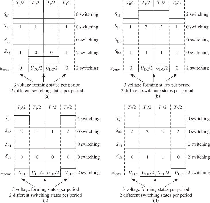
Figure 23.5 Duty cycles for H-DCC with 1D-N2V modulation generating  output voltage level: (a) and (b) positive lower
  , (c) and (d) positive upper ½
 for
for  and
and  redundant switching state selections, respectively

Figure 23.6 Duty cycles for the H-DCC with 1D-N3V modulation generating  output voltage level: (a) positive lower
  and (b) positive upper ½
 .
.
Another modulation technique for H-DCC is the 1D-N3V. Figure 23.6 presents the positive output voltage-switching patterns for 1D-N3V modulation, which is based on the assumption that both redundant switching states, for whichever output voltage level ![]() are applied in each sampling period [20 26, 27]. The 1D-N3V modulation allows symmetrical duty cycle placement to be obtained for the seven (see Figure 23.6(a)) and five (see Figure 23.6(b)) output voltage
are applied in each sampling period [20 26, 27]. The 1D-N3V modulation allows symmetrical duty cycle placement to be obtained for the seven (see Figure 23.6(a)) and five (see Figure 23.6(b)) output voltage ![]() forming states for lower and upper output voltage levels, respectively. Redundant switching states are applied for the appropriate part of the calculated time
forming states for lower and upper output voltage levels, respectively. Redundant switching states are applied for the appropriate part of the calculated time ![]() , which corresponds to the voltage ratio between DC-link capacitors
, which corresponds to the voltage ratio between DC-link capacitors ![]() and
and ![]() . It means that if
. It means that if ![]() is larger than
is larger than ![]() ,
, ![]() will be charged less than
will be charged less than ![]() . The ratio of
. The ratio of ![]() charging time division of
charging time division of ![]()
![]() and
and ![]()
![]() is inversely proportional to the ratio of the
is inversely proportional to the ratio of the ![]() and
and ![]() voltages:
voltages:
where ![]() . As a result, during the sampling period, both DC-link capacitors over the calculated time
. As a result, during the sampling period, both DC-link capacitors over the calculated time ![]() will be charged or discharged.
will be charged or discharged.
It should be noted that the self-balancing of the DC-link capacitors with a symmetrical distribution of ![]() , even for balanced
, even for balanced ![]() and
and ![]() voltages, is not possible in practice because of:
voltages, is not possible in practice because of:
- nonlinear IGBT gate signal propagation,
- different IGBT ON/OFF times,
- DC-link capacitor equivalent series and parallel resistances,
- differences in electrical parameters, such as each leg's semiconductor devices and connection points.
Therefore, an additional controller (proportional or proportional-integral (PI)) should be used in order to determine the distribution of ![]() , providing the equalization of the
, providing the equalization of the ![]() and
and ![]() voltages.
voltages.
23.2.3 H-Flying Capacitor Converter (H-FCC)
Figure 23.7 presents the single-phase H-FCC [28–30], which has two legs, with IGBTs denoted ![]() ,
, ![]() ,
, ![]() and
and ![]() , where
, where ![]() and
and ![]() are the negation of
are the negation of ![]() , respectively and
, respectively and ![]() is the leg indication:
is the leg indication: ![]() or
or ![]() . The so-called FC
. The so-called FC ![]() are parallel connected to
are parallel connected to ![]() and
and ![]() for each leg. The FCs are used to generate the intermediate H-FCC voltage levels, which can be obtained – in contrast to the H-DCC – separately for each leg from the other leg-switching states. Balancing of the FC voltages uses two redundant switching states for each H-FCC leg and is independent of the switching states in the other leg.
for each leg. The FCs are used to generate the intermediate H-FCC voltage levels, which can be obtained – in contrast to the H-DCC – separately for each leg from the other leg-switching states. Balancing of the FC voltages uses two redundant switching states for each H-FCC leg and is independent of the switching states in the other leg.

Figure 23.7 Single-phase five-level H-flying capacitor converter
Four different switching states (including two redundant states for FC voltage balancing), generating three different output pole voltages can be distinguished for a single leg of the converter:
- 0, when
 and
and  are turned OFF (output pole voltage equals 0),
 - 1, when:
 is tuned OFF and
  is turned ON,
 is tuned ON and
  is turned OFF,
where both generate the same
 output pole voltage (depending on the selected state,
  or
or  ),
), - 2, when
 and
and  are turned ON (output pole voltage equals
  ).
).
Table 23.4 Switching states for H-FCC
| Switch number | Levels of output voltage |
|||||||||||||||
| ½ |
||||||||||||||||
| 0 | 0 | 0 | 0 | 1 | 0 | 0 | 1 | 1 | 0 | 1 | 0 | 1 | 1 | 1 | 1 | |
| 0 | 0 | 0 | 1 | 0 | 0 | 1 | 0 | 0 | 1 | 1 | 1 | 0 | 1 | 1 | 1 | |
| 1 | 0 | 1 | 1 | 1 | 0 | 0 | 0 | 1 | 1 | 1 | 0 | 0 | 0 | 1 | 0 | |
| 1 | 1 | 0 | 1 | 1 | 0 | 1 | 1 | 0 | 0 | 1 | 0 | 0 | 1 | 0 | 0 | |
In the case of the single-phase H-FCC, it gives 16 possible switching state combinations. Thus, the H-FCC allows five levels of module ![]() output voltage to be obtained (Table 23.4): six redundant for
output voltage to be obtained (Table 23.4): six redundant for ![]() , four redundant for whichever
, four redundant for whichever ![]() , and one for whichever
, and one for whichever ![]() . Which output voltage level is applied is dependent on
. Which output voltage level is applied is dependent on ![]() (Equations 23.1 and 23.6). For every
(Equations 23.1 and 23.6). For every ![]() level, the switching state duration times are assigned as follows:
level, the switching state duration times are assigned as follows:
 for
for  ,
, for
for  , which can be divided – with respect to the modulation technique used – into two times:
  and
and  (where
  ) assigned for leg
  and
and  , respectively (in each sampling period only one or two FC capacitors can be used in order to fulfill the modulation objectives),
 for
for  ,
,
and are calculated in the same way as for the H-DCC (Equations 23.7–23.9, 23.10).
As mentioned earlier, in order to provide proper H-FCC operation, the voltage on each FC capacitor should be stabilized on ½![]() . The balancing of single FC voltage
. The balancing of single FC voltage ![]() or
or ![]() is independent of the switching state in the other leg. Therefore, switching states – depending on the output voltage level and sign of the line current – used only for FC voltage balancing in leg
is independent of the switching state in the other leg. Therefore, switching states – depending on the output voltage level and sign of the line current – used only for FC voltage balancing in leg ![]() (leg
(leg ![]() is similar) are shown in Table 23.5.
is similar) are shown in Table 23.5.
Table 23.5 H-FCC switching states used for ![]() capacitor voltage balancing
capacitor voltage balancing
| Output voltage |
DC-link voltages | Line current | Switching state | |||
| ½ |
1 | 0 | 0 | 0 | ||
| 0 | 1 | 0 | 0 | |||
| 0 | 1 | 0 | 0 | |||
| 1 | 0 | 0 | 0 | |||
| 0 | 1 | 1 | 1 | |||
| 1 | 0 | 1 | 1 | |||
| 1 | 0 | 1 | 1 | |||
| 0 | 1 | 1 | 1 | |||
For each sampling period:
- one (over the entire calculated time
 , when only one FC is used),
 - two (each at time
 and
and  , when both FCs are used),
 - all four (each at the appropriate part of the calculated times
 and
and  )
)
redundant states affecting the FC capacitor voltages can be used. Switching state selection and duration time depend on the applied PWM technique: 1D-N2V, 1D-N3V, or 1D-N(3 + 2R)V modulations, respectively.
1D-N2V modulation is based on the assumption that only two switching states are applied in each sampling period, when only one leg is pulse-width modulated [20 26]. Which leg is switched depends on the sign of ![]() , similar to the parallel-connected H-BC (Equation 23.5). As a consequence, for a positive sign of
, similar to the parallel-connected H-BC (Equation 23.5). As a consequence, for a positive sign of ![]() , only one of two, whichever
, only one of two, whichever ![]() , redundant states for each lower or upper voltage level is selected. The duration of redundant state
, redundant states for each lower or upper voltage level is selected. The duration of redundant state ![]() in leg
in leg ![]() is equal to
is equal to ![]() with proper
with proper ![]() and
and ![]() output voltage switching states. Leg
output voltage switching states. Leg ![]() is permanently in the
is permanently in the ![]() state. The selection of one of two possible redundant states for leg
state. The selection of one of two possible redundant states for leg ![]() depends on the conditions given in Table 23.5. If
depends on the conditions given in Table 23.5. If ![]() has a negative sign, the opposite situation occurs – leg
has a negative sign, the opposite situation occurs – leg ![]() is modulated and leg
is modulated and leg ![]() is permanently in the
is permanently in the ![]() state. To reduce the number of switching between
state. To reduce the number of switching between ![]() and redundant
and redundant ![]() output voltage state, the
output voltage state, the ![]()
![]() state is chosen from six redundant
state is chosen from six redundant ![]() output voltage states (Tables 23.4 and 23.6). The reduced switching states of the 1D-N2V modulation are presented in Table 23.6. Figure 23.8 presents the positive output voltage-switching patterns for the H-FCC with the 1D-N2V modulation. It allows symmetrical duty cycle placement to be obtained for the three forming states of the output voltage
output voltage states (Tables 23.4 and 23.6). The reduced switching states of the 1D-N2V modulation are presented in Table 23.6. Figure 23.8 presents the positive output voltage-switching patterns for the H-FCC with the 1D-N2V modulation. It allows symmetrical duty cycle placement to be obtained for the three forming states of the output voltage ![]() for all levels, with two different switching states used in each sampling period.
for all levels, with two different switching states used in each sampling period.
Table 23.6 Switching states for H-FCC with 1D-N2V modulation
| Switch number | Levels of output voltage |
||||||
| ½ |
|||||||
| 0 | 0 | 0 | 0 | 1 | 0 | 1 | |
| 0 | 0 | 0 | 0 | 0 | 1 | 1 | |
| 1 | 1 | 0 | 0 | 0 | 0 | 0 | |
| 1 | 0 | 1 | 0 | 0 | 0 | 0 | |

Figure 23.8 Duty cycles for the H-FCC with 1D-N2V modulation generating  output voltage level: (a) positive lower
  and (b) positive upper ½
The next type, the 1D-N3V modulation, is based on the assumption that both legs, ![]() and
and ![]() , are working in each sampling period to generate the output voltage level
, are working in each sampling period to generate the output voltage level ![]() [20 26, 27]. However, for each leg only one of two, whichever
[20 26, 27]. However, for each leg only one of two, whichever ![]() , redundant states for the lower or upper voltage level is selected over the calculated time
, redundant states for the lower or upper voltage level is selected over the calculated time ![]() equal to ½
equal to ½![]() . Switching state selection for leg
. Switching state selection for leg ![]() depends – similar to 1D-N2V modulation – on the conditions given in Table 23.5. Such a selection results in four possible combinations of switching states generating output voltage
depends – similar to 1D-N2V modulation – on the conditions given in Table 23.5. Such a selection results in four possible combinations of switching states generating output voltage ![]() . To reduce the number of switching between output voltage
. To reduce the number of switching between output voltage ![]() and
and ![]() , for each aforementioned combination, only two (from six redundant
, for each aforementioned combination, only two (from six redundant ![]() output voltage states) are chosen:
output voltage states) are chosen:
- one permanently:

 or
or 
 (for positive and negative voltage levels, respectively),
 - one depending on the selected combination:
 for
for  and
and  ,
,  for
for  and
and  ,
,  for
for  and
and  and finally
  for
for  and
and  .
.
All lower ![]() and upper ½
and upper ½![]() positive output voltage level switching state combinations are shown in Figures 23.9 and 23.10, respectively.
positive output voltage level switching state combinations are shown in Figures 23.9 and 23.10, respectively.

Figure 23.9 Duty cycles for the H-FCC with 1D-N3V modulation generating  lower positive output voltage level
  with different redundant switching states

Figure 23.10 Duty cycles for the H-FCC with 1D-N3V modulation generating  positive upper output voltage level ½
 with different redundant switching states
The symmetrical duty cycle placement of the four different switching states used for the lower output voltage level gives seven forming states of output voltage ![]() (Figure 23.9), but the upper positive voltage level redundant states are placed nonsymmetrically with respect to the middle of the sampling period; however, the output pulses of
(Figure 23.9), but the upper positive voltage level redundant states are placed nonsymmetrically with respect to the middle of the sampling period; however, the output pulses of ![]() are generated symmetrically (Figure 23.10). Three different switching states used for the generation of the upper
are generated symmetrically (Figure 23.10). Three different switching states used for the generation of the upper ![]() levels (combination of redundant intermediate with the proper
levels (combination of redundant intermediate with the proper ![]() or
or ![]() state) gives five forming states of the
state) gives five forming states of the ![]() voltage.
voltage.

Figure 23.11 Duty cycles for the H-FCC with 1D-N(3 + 2R)V modulation generating  output voltage level: (a) positive lower
  and (b) positive upper ½
It is possible to increase the H-FCC output pulse frequency over the frequency generated by the 1D-N3V modulation, which is not possible for the H-DCC. This can be achieved by the method proposed in Ref. [31] the 1D-N(3 + 2R)V modulation. The 1D-N(3 + 2R)V modulation is based on the assumption that in every sampling period all four redundant ![]() output voltage switching states are used (Figure 23.11). As a result, both FCs are charged and discharged in each period, where the redundant switching state charging and discharging of the FCs are applied for the appropriate part of the calculated time
output voltage switching states are used (Figure 23.11). As a result, both FCs are charged and discharged in each period, where the redundant switching state charging and discharging of the FCs are applied for the appropriate part of the calculated time ![]() (for
(for ![]() and
and ![]() , respectively) equal to ½
, respectively) equal to ½![]() . It means, for example, that if
. It means, for example, that if ![]() is bigger than ½
is bigger than ½![]() ,
, ![]() will be more charged than discharged. The ratio of
will be more charged than discharged. The ratio of ![]() and
and ![]() between charging
between charging ![]() and discharging
and discharging ![]() state time division is a proportional function of
state time division is a proportional function of ![]() and FC voltages
and FC voltages ![]() and
and ![]() :
:
where ![]() . Such an approach to the nonsymmetrical switching of each IGBTs allows the same output voltage waveform to be obtained as for the parallel-connected H-BC with UPWM – nine forming states of output voltage
. Such an approach to the nonsymmetrical switching of each IGBTs allows the same output voltage waveform to be obtained as for the parallel-connected H-BC with UPWM – nine forming states of output voltage ![]() for all output voltage levels with:
for all output voltage levels with:
- eight different switching states used per period for the lower
 output voltage,
 - five different switching states used per period for the upper
 output voltage.
The self-balancing of the FC voltages (assuming ![]() and
and ![]() ) is not possible in practice, for reasons similar to the 1D-N3V modulation for H-DCC (in addition to the FC's equivalent series and parallel resistances).
) is not possible in practice, for reasons similar to the 1D-N3V modulation for H-DCC (in addition to the FC's equivalent series and parallel resistances).
23.2.4 Comparison
The reference for the comparison study of the single-phase VSC topologies and PWM techniques presented is the single-phase parallel-connected H-BC with unipolar modulation used in RTPSs. Such a converter, owing to interleaved modulation, provides an increased number of output voltage ![]() forming states and very low current harmonics distortion on the transformer high-voltage side.
forming states and very low current harmonics distortion on the transformer high-voltage side.
Table 23.7 presents the number of output voltage ![]() forming states visible from the transformer high-voltage side and the number of total switching states used in the sampling period to generate the
forming states visible from the transformer high-voltage side and the number of total switching states used in the sampling period to generate the ![]() voltage waveform. The comparison of PWM techniques shows the clear advantage of the parallel-connected H-BC with the UPWM and the H-FCC with the 1D-N(3 + 2R)V modulation with respect to the highest number of forming states.
voltage waveform. The comparison of PWM techniques shows the clear advantage of the parallel-connected H-BC with the UPWM and the H-FCC with the 1D-N(3 + 2R)V modulation with respect to the highest number of forming states.
Table 23.7 Number of output voltage ![]() forming states/switching per period
forming states/switching per period
| PC-H-BC | H-DCC | H-FCC | ||||
| HPWM | UPWM | 1D-N2V | 1D-N3V | 1D-N2V | 1D-N3V | 1D-N(3 + 2R)V |
| Lower levels of output voltage |
||||||
| 5/4 | 9/8 | 3/2 | 7/6 | 3/2 | 7/6 | 9/8 |
| Upper levels of output voltage |
||||||
| 5/4 | 9/8 | 3/2 | 5/4 | 3/2 | 5/4 | 9/8 |
Figures 23.13–23.15 present the steady-state operation of the 1 MW parallel-connected H-BC, H-DCC and H-FCC with the UPWM, 1D-N3V and the 1D-N(3 + 2R)V modulations, respectively. The simplified simulation model for the aforementioned cases is shown in Figure 23.12, with the main electrical parameters of the power circuits and control data given in Table 23.8. For all cases, the converter voltage harmonics distortion ![]() factor is similar. However, with respect to 1 kHz sampling frequency bands related to the output pulse's frequency:
factor is similar. However, with respect to 1 kHz sampling frequency bands related to the output pulse's frequency:
- quadrupled for the parallel-connected H-BC (Figure 23.13(e-f)),
- doubled for the lower (Figure 23.14(e)) and tripled for the upper (Figure 23.14(f)) output voltage levels for the H-DCC,
- quadrupled for the H-FCC (Figure 23.15(e-f)),

Figure 23.12 Simplified model of 1 MW single-phase converters: (a) parallel-connected H-BC, (b) H-DCC and (c) H-FCC
Table 23.8 Parameters of 1 MW single-phase converters: PC-H-BC, H-DCC and H-FCC
| Simulation parameter | Symbol | Value | ||
| Topology | PC-H-BC | H-DCC | H-FCC | |
| Transformer power/primary side | 1 MVA | |||
| Grid voltage/primary side | 25 kV/50 Hz | |||
| Grid current/primary side | 40 A | |||
| Transformer power/secondary sides | 500 kVA | 1 MVA | ||
| Line voltage/secondary sides | 950 V/50 Hz | 1900 V/50 Hz | ||
| Line current/secondary sides | 526 A | 1052 A | ||
| Primary leakage inductance | 24 mH | |||
| Primary winding resistance | 3 Ω | |||
| Magnetizing inductance | 24 H | |||
| Core loss resistance | 60 kΩ | |||
| Secondary leakage inductance | 1.44 mH | 0.72 mH | ||
| Secondary winding resistance | 15 mΩ | |||
| Sampling frequency | 1 kHz | |||
| Capacitance of DC-link capacitors | 23.4 mF | 46.8 mF | 23.4mF | |
| DC-link voltage | 1800 V | |||
| Capacitance of flying capacitors | 11.7 mF | |||

Figure 23.13 Operation of parallel-connected H-BC with UPWM: (a) grid voltage  and current
  , (b) converter voltage
  and DC-link voltage
  , (c) module 1 line voltage
  and current
  , (d) module 1 and 2 voltage
  and
and  (e) and (f) two periods zoom for lower and upper
  converter voltage level and grid current
  and (g) grid current and converter voltage harmonics

Figure 23.14 Operation of H-DCC with 1D-N3V: (a) grid voltage  and current
  , (b) converter voltage
  and DC-link voltage
  , (c) line voltage
  and current
  , (d) upper and lower DC-link capacitor voltage
  and
and  , (e) and (f) two periods zoom for lower and upper
  converter voltage level and grid current
  (g) grid current and converter voltage harmonics spectrum
  and
and  .
.

Figure 23.15 Operation of H-FCC with 1D-N(3 + 2R)V: (a) grid voltage  and current
  , (b) converter voltage
  and DC-link voltage
  , (c) line voltage
  and current
  , (d) flying capacitor voltages
  and
and  , (e) and (f) two periods zoom for lower and upper
  converter voltage level and grid current
  and (g) grid current and converter voltage harmonics spectrum
  and
and  .
.
shifting in the direction of higher harmonics can be observed:
- 4 kHz for the parallel-connected H-BC (Figure 23.13(g)),
- 2 kHz and 3 kHz for the H-DCC (Figure 23.14(g)),
- 4 kHz for the H-FCC (Figure 23.15(g)).
Thus, a similar voltage distortion ![]() factor for higher frequencies provides a lower harmonics distortion of the grid current.
factor for higher frequencies provides a lower harmonics distortion of the grid current.
Table 23.9 Comparison of grid current distortion ![]()
| PC-H-BC | H-DCC | H-FCC | ||||
| HPWM | UPWM | 1D-N2V | 1D-N3V | 1D-N2V | 1D-N3V | 1D-N(3 + 2R)V |
| 1 MW output power, 100% load, |
||||||
| 3.11% | 2.03% | 6.93% | 3.61% | 6.47% | 3.46% | 2.11% |
| 0.33 MW output power, 33% load, |
||||||
| 8.39% | 5.30% | 21.13% | 9.78% | 17.66% | 9.56% | 6.46% |
Table 23.9 presents a comparison of the grid current distortion ![]() for all topologies and modulation techniques presented, with different load values. It can be observed that the parallel-connected H-BC with the UPWM, as well as the H-FCC with 1D-N(3 + 2R)V PWM modulation – thanks to the increased number of output voltage
for all topologies and modulation techniques presented, with different load values. It can be observed that the parallel-connected H-BC with the UPWM, as well as the H-FCC with 1D-N(3 + 2R)V PWM modulation – thanks to the increased number of output voltage ![]() forming states – provides the lowest grid current distortion
forming states – provides the lowest grid current distortion ![]() . However, if the H-FCC with 1D-N(3 + 2R)V modulation and parallel-connected H-BC with UPWM:
. However, if the H-FCC with 1D-N(3 + 2R)V modulation and parallel-connected H-BC with UPWM:
- provide similar harmonics injection into the power system,
- uses all switches in the sampling period to generate output voltage,
- uses the same voltage and current class semiconductors (which guarantees similar switching losses),
the advantages of the H-FCC solution are:
- a reduced number of transformer low-voltage side windings,
- a reduced transformer volume, size and weight,
- component price reductions due to the decreased voltage class semiconductors.
On the other hand, the parallel-connected H-BC has a high reliability in the case of one module failure – the VSC works with the same amplitude of ![]() but with twice reduced power and with an increased THD factor of
but with twice reduced power and with an increased THD factor of ![]() . For the H-FCC in the case of one leg failure (as well as for the H-DCC), there is the possibility of switching off the broken leg and connecting the phase from the broken leg to the midpoint of the connection of the DC-link capacitors. The advantage of such a solution is that full power is delivered to the load, but of course at the cost of an increased THD factor of the
. For the H-FCC in the case of one leg failure (as well as for the H-DCC), there is the possibility of switching off the broken leg and connecting the phase from the broken leg to the midpoint of the connection of the DC-link capacitors. The advantage of such a solution is that full power is delivered to the load, but of course at the cost of an increased THD factor of the ![]() However, it is necessary to modify the PWM strategy, which is not required with the parallel-connected H-BC.
However, it is necessary to modify the PWM strategy, which is not required with the parallel-connected H-BC.
23.3 Control of AC–DC Single-Phase Voltage Source Converters
Figure 23.16 presents the single-phase equivalent circuit of the VSC. According to Figure 23.16, the VSC can be described as:

Figure 23.16 Single-phase equivalent circuit of the voltage source converter
where the voltage drop in inductor ![]() is defined as:
is defined as:
and ![]() and
and ![]() denote, respectively, the inductance and resistance of the inductor. The converter output voltage
denote, respectively, the inductance and resistance of the inductor. The converter output voltage ![]() is controllable and depends on the applied switching states'
is controllable and depends on the applied switching states' ![]() table (e.g., Tables 23.1 23.2 and 23.4), constructed by the individual switching states and DC-link voltage level (Figure 23.17):
table (e.g., Tables 23.1 23.2 and 23.4), constructed by the individual switching states and DC-link voltage level (Figure 23.17):

Figure 23.17 Simplified current control structure of single-phase VSC
Owing to changes in the ![]() magnitude and phase, the voltage drop on the inductor
magnitude and phase, the voltage drop on the inductor ![]() can be controlled directly and thus the line current
can be controlled directly and thus the line current ![]() can be controlled indirectly. Figure 23.17 presents a simplified current control structure for the single-phase VSC, which consists of inner current control loop and the outer voltage control loop. Synchronization with grid voltage for high (including unity) input power factor operation is provided by a phase-locked loop (PLL) algorithm.
can be controlled indirectly. Figure 23.17 presents a simplified current control structure for the single-phase VSC, which consists of inner current control loop and the outer voltage control loop. Synchronization with grid voltage for high (including unity) input power factor operation is provided by a phase-locked loop (PLL) algorithm.
Figure 23.18 presents the general phasor diagrams of the VSC for the rectifier and inverter modes of operation, with and without unity power factor conditions, according to Equation (23.13). The goal of the outer voltage control loop is to regulate the DC-link voltage ![]() to follow reference value
to follow reference value ![]() , while the inner current control loop is designed to keep line current
, while the inner current control loop is designed to keep line current ![]() sinusoidal and in phase with line voltage
sinusoidal and in phase with line voltage ![]() . This means that the current control should provide VSC unity power factor for rectification and inverting modes of operation.
. This means that the current control should provide VSC unity power factor for rectification and inverting modes of operation.

Figure 23.18 Phasor diagrams of the VSC for: (a), (c) rectification mode, (b), (d) invertering mode, (a), (b) nonunity power factor, (c), (d) unity power factor
23.3.1 Single-Phase Control Algorithm Classification
The current control should ensure a constant switching frequency with a specified switching pattern from a filter design point of view. This requirement can only be satisfied with PWM-based current control, allowing the implementation of modern PWM techniques [32]. Unless high dynamic requirements are given, a linear controller is the most suitable for PWM-based current control. Linear controllers are designed on an average model of the converter based on PWM, which is responsible for the transformation of continuous switching functions into discrete switching pattern functions. Two such systems, PI- and proportional-resonant (PR) based current control (PI-CC and PR-CC, respectively) schemes, have gained superior position [33–36].
PI-based current control is mainly used in ![]() synchronous reference frame rotating with the grid voltage, in which control variables become DC values. The PI controller – composed of proportional gain and an integrator – tracking DC reference is able to eliminate steady-state error. However, in
synchronous reference frame rotating with the grid voltage, in which control variables become DC values. The PI controller – composed of proportional gain and an integrator – tracking DC reference is able to eliminate steady-state error. However, in ![]() natural reference frame, the PI controller exhibits two well-known drawbacks: the inability to track the AC reference without steady-state error and poor disturbance rejection capability.
natural reference frame, the PI controller exhibits two well-known drawbacks: the inability to track the AC reference without steady-state error and poor disturbance rejection capability.
The tracking of periodical signals and rejection of periodical disturbances problem in the ![]() natural reference frame can be solved by using PR-based current control. A PR controller – composed of proportional gain and a resonant integrator – achieves a very high gain around the resonance frequency and almost no gain outside this frequency. Therefore, the PR controller is capable of not only eliminating steady-state amplitude but also phase error. The implementation of a PR controller in
natural reference frame can be solved by using PR-based current control. A PR controller – composed of proportional gain and a resonant integrator – achieves a very high gain around the resonance frequency and almost no gain outside this frequency. Therefore, the PR controller is capable of not only eliminating steady-state amplitude but also phase error. The implementation of a PR controller in ![]() natural reference frame is straightforward, and in comparison to PI-based control the complexity of the control algorithm is considerably reduced.
natural reference frame is straightforward, and in comparison to PI-based control the complexity of the control algorithm is considerably reduced.
As far as PR-CC can be used directly, for PI-CC a transformation from a natural to synchronous reference frame is needed. In three-phase systems, coordinate transformation is straightforward. However, in single-phase, it is necessary to create a second quantity in-quadrature with the real one. There are a few mathematical methods available to achieve a set of in-quadrature signals based on the measured single-phase grid voltage [37 38]:
 transport delay technique, where
  is the fundamental grid frequency period,
- Hilbert transform,
- inverse Park transform.
These methods, while allowing for correct quadrature signal generation (QSG), are complex, nonlinear and significantly dependent on fundamental grid frequency changes. Algorithms that are able to eliminate these drawbacks are based on adaptive filtering, allowing in-quadrature generation based both on the phase and frequency synchronization: the second-order adaptive filter and the second-order generalized integrator (SOGI), of which SOGI is most suitable [39].
Synchronization with grid voltage for high (including unity) input power factor operation for both CC methods is also needed. The typical hardware solution with grid voltage zero crossing detection (discontinuous and dependent on the occurrence of the event) is based on line voltage measurement. Filtering of the measured signal in order to determine the zero crossing generates errors, because of the low speed of synchronization and possible distortions arising from the zero crossing detection under distorted voltage. Solutions based on mathematical algorithms – PLLs – allow for fast and accurate synchronization while eliminating the influence of interferences. PLL needs in-quadrature signals, which can be obtained for a single-phase system with SOGI. The SOGI-PLL detects the input phase-angle faster than conventional PLL without steady-state oscillations [39].
As mentioned, unlike PR-CC, a PI-CC transformation from natural to synchronous reference frame is needed. As for both solutions PLL is necessary, the SOGI does not increase the complexity of the control algorithm. However, coordinate transformation from ![]() to
to ![]() and then inverse transformation is necessary for PI-CC, which makes it more complicated.
and then inverse transformation is necessary for PI-CC, which makes it more complicated.
Another important issue for current control is the ability to compensate grid harmonics in order to improve power quality. Power quality – beyond the control of amplitude and phase – is one of the responsibilities of current controllers. In ![]() , synchronous coordinates harmonics compensation is based on low-pass and high-pass filtering with PI regulators. For specific harmonic coordinates, frame rotating with harmonic frequency should be implemented. Filtered signals are controlled by two PI regulators in
, synchronous coordinates harmonics compensation is based on low-pass and high-pass filtering with PI regulators. For specific harmonic coordinates, frame rotating with harmonic frequency should be implemented. Filtered signals are controlled by two PI regulators in ![]() coordinates and again transformed to rotating coordinates with fundamental frequency. The obtained signals are added to signals referenced for the PWM modulator. In
coordinates and again transformed to rotating coordinates with fundamental frequency. The obtained signals are added to signals referenced for the PWM modulator. In ![]() natural reference frame harmonics, compensation is based on a resonant controller. For specific harmonics, there is no need for additional coordinate transformation and filtering. For single harmonics, an additional resonant controller is parallel connected to a fundamental frequency PR controller. Thus, in
natural reference frame harmonics, compensation is based on a resonant controller. For specific harmonics, there is no need for additional coordinate transformation and filtering. For single harmonics, an additional resonant controller is parallel connected to a fundamental frequency PR controller. Thus, in ![]() coordinates, two PI controllers are needed, whereas in
coordinates, two PI controllers are needed, whereas in ![]() only one resonant part is used.
only one resonant part is used.
In this section, the basic structures of the ![]() synchronous reference frame current control, PI-CC, and the
synchronous reference frame current control, PI-CC, and the ![]() natural reference frame current control, PR-CC, are presented. Moreover, the development of current and DC-link voltage controllers with tuning methods for PI, PR, and PMR is discussed. Ultimately, the APFF algorithm used to improve the dynamics of the DC-link stabilization is presented.
natural reference frame current control, PR-CC, are presented. Moreover, the development of current and DC-link voltage controllers with tuning methods for PI, PR, and PMR is discussed. Ultimately, the APFF algorithm used to improve the dynamics of the DC-link stabilization is presented.
23.3.2 DQ Synchronous Reference Frame Current Control – PI-CC
A characteristic feature for ![]() synchronous reference frame current control is coordinate transformation from stationary to synchronous rotating
synchronous reference frame current control is coordinate transformation from stationary to synchronous rotating ![]() and opposite from
and opposite from ![]() , which is very natural for a three-phase system:
, which is very natural for a three-phase system:


where an angle of the voltage vector ![]() is defined as
is defined as

The line current vector ![]() is split into two rectangular components
is split into two rectangular components ![]() in voltage-oriented
in voltage-oriented ![]() coordinates (Figure 23.19). The component
coordinates (Figure 23.19). The component ![]() determinates the reactive power, whereas
determinates the reactive power, whereas ![]() determines the active power flow. Thus, the reactive and the active power can be controlled independently. Unity power factor operation can be achieved when the line current vector
determines the active power flow. Thus, the reactive and the active power can be controlled independently. Unity power factor operation can be achieved when the line current vector ![]() is aligned with the line voltage vector
is aligned with the line voltage vector ![]() .
.

Figure 23.19 Coordinate transformation of line current vector  and line voltage vector
  from stationary
  to synchronous rotating
  reference frame coordinates
The situation is slightly more complicated in the case of a single-phase system, because the coordinates are virtual and need special algorithms to obtain the ![]() or
or ![]() system. Among the most attractive solutions is a method based on delaying the
system. Among the most attractive solutions is a method based on delaying the ![]() -axis by ¼ of a line voltage period to obtain the
-axis by ¼ of a line voltage period to obtain the ![]() -axis (Figure 23.20(a)) or the use of notch filters with a narrow stop-band (e.g., second-order Butterworth) tuned at twice the line frequency [40 41] (Figure 23.20(b)).
-axis (Figure 23.20(a)) or the use of notch filters with a narrow stop-band (e.g., second-order Butterworth) tuned at twice the line frequency [40 41] (Figure 23.20(b)).

Figure 23.20 Methods to obtain a virtual  synchronous rotating coordinate system in single-phase converter: (a) based on ¼ delay of
  -axis and (b) based on two notch filters tuned at twice the line frequency
The voltage equations (Equation 23.13) in the ![]() synchronous reference frame in accordance with the presented transformation (Equations 23.16 and 23.17) are as follows:
synchronous reference frame in accordance with the presented transformation (Equations 23.16 and 23.17) are as follows:

The block diagram of the control for the single-phase converter in the ![]() synchronous reference frame is shown in Figure 23.21. Measured
synchronous reference frame is shown in Figure 23.21. Measured ![]() and
and ![]() currents are compared with reference values
currents are compared with reference values ![]() and
and ![]() and the error is delivered to the PI controllers. Then, the decoupling terms
and the error is delivered to the PI controllers. Then, the decoupling terms ![]() and
and ![]() are applied according to Equation (23.19). Finally, based on Equation (23.17), converter reference voltages in the stationary coordinate system are calculated, where
are applied according to Equation (23.19). Finally, based on Equation (23.17), converter reference voltages in the stationary coordinate system are calculated, where ![]() is used by the modulator and
is used by the modulator and ![]() is discarded:
is discarded:

Figure 23.21 Classical single-phase control in virtual  synchronous rotating coordinate system

Figure 23.22 Simplified single-phase control in virtual  synchronous rotating coordinate system
The control presented in Figure 23.21 can be significantly simplified, as shown in Figure 23.22 [42]. Thanks to the simple assumption that for a virtual ![]() -axis error of current control
-axis error of current control ![]() is equal to zero, the following equations:
is equal to zero, the following equations:


can be simplified to form:
Thanks to this, only a simple PLL is needed to obtain the synchronous rotating coordinate system instead of using coordinate transformations from stationary to synchronous rotating ![]() (Equation 23.17), notch filters or storing samples to get a quarter cycle delay.
(Equation 23.17), notch filters or storing samples to get a quarter cycle delay.
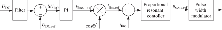
Figure 23.23 Block scheme of PR controller-based current control algorithm
23.3.3 ABC Natural Reference Frame Current Control – PR-CC
Figure 23.23 presents the block scheme of the PR controller-based current control algorithm, which consists of two cascaded loops. The commanded DC-link voltage ![]() is compared with the measured
is compared with the measured ![]() value. The voltage
value. The voltage ![]() is distorted by 100 Hz AC oscillations derived from the single-phase current
is distorted by 100 Hz AC oscillations derived from the single-phase current ![]() with 50 Hz fundamental frequency. Because the
with 50 Hz fundamental frequency. Because the ![]() has a constant DC value, the 100 Hz distortion will be visible in the DC-link voltage error signal
has a constant DC value, the 100 Hz distortion will be visible in the DC-link voltage error signal ![]() . The
. The ![]() signal is delivered to the PI controller, which generates the reference line current amplitude
signal is delivered to the PI controller, which generates the reference line current amplitude ![]() . As the PI regulator is not able to eliminate phase error, in order to prevent transmission of 100 Hz distortion on the current
. As the PI regulator is not able to eliminate phase error, in order to prevent transmission of 100 Hz distortion on the current ![]() , a low-pass filter with 30 Hz cutoff frequency is applied on the measured
, a low-pass filter with 30 Hz cutoff frequency is applied on the measured ![]() voltage. The delay introduced by the filter causes a reduction in the voltage loop dynamics, and as a consequence the DC-link voltage transient error should be higher. In fact, for a low switching frequency, the step change response of the DC-link PI controller with and without a low-pass filter is similar. The reason is the limited bandwidth of the voltage loop, which is more restrictive than the bandwidth reduction introduced by the filter. However, for higher sampling frequencies, the dynamics of the voltage loop will be reduced. It should also be noted that for a low sampling frequency the time of the step response will be longer than in the case of a high sampling frequency. To improve the dynamics of the DC-link stabilization, the power feed-forward signal (containing information about the load changes) should be added to the output signal of the DC-link voltage controller (see Section 23.3.4). APFF provides very good stabilization of the DC-link voltage in transient states, and the DC-link voltage overshoot is significantly reduced.
voltage. The delay introduced by the filter causes a reduction in the voltage loop dynamics, and as a consequence the DC-link voltage transient error should be higher. In fact, for a low switching frequency, the step change response of the DC-link PI controller with and without a low-pass filter is similar. The reason is the limited bandwidth of the voltage loop, which is more restrictive than the bandwidth reduction introduced by the filter. However, for higher sampling frequencies, the dynamics of the voltage loop will be reduced. It should also be noted that for a low sampling frequency the time of the step response will be longer than in the case of a high sampling frequency. To improve the dynamics of the DC-link stabilization, the power feed-forward signal (containing information about the load changes) should be added to the output signal of the DC-link voltage controller (see Section 23.3.4). APFF provides very good stabilization of the DC-link voltage in transient states, and the DC-link voltage overshoot is significantly reduced.
The internal current loop is responsible for system power quality by controlling the grid current. In PR-CC, unity power factor operation can be achieved if the reference line current ![]() is given as:
is given as:
The cosinus function is used because of the SOGI-PLL phase-angle ![]() generation –
generation – ![]() when the
when the ![]() amplitude has the maximum positive value. The reference value of
amplitude has the maximum positive value. The reference value of ![]() is compared with the measured line current
is compared with the measured line current ![]() and the error is delivered to the PR controller. The PR structure shown in Figure 23.24(a) is composed of proportional gain and a resonant integrator [33 36].
and the error is delivered to the PR controller. The PR structure shown in Figure 23.24(a) is composed of proportional gain and a resonant integrator [33 36].

Figure 23.24 Block diagram of: (a) proportional resonant (PR) controller and (b) proportional multiresonant (PMR) controller
The core of the resonant integrator is the generalized integrator, which achieves a very high gain around the resonant frequency and almost no gain outside this frequency. The transfer function of an ideal PR controller is given by:
where ![]() is the proportional gain and
is the proportional gain and ![]() is the gain of the resonant integrator. The transfer function of the PR controller contains a double imaginary pole adjusted to the fundamental
is the gain of the resonant integrator. The transfer function of the PR controller contains a double imaginary pole adjusted to the fundamental ![]() frequency
frequency ![]() . Thus, the PR controller is able to track the input phase angle for
. Thus, the PR controller is able to track the input phase angle for ![]() without any steady-state error. Note that the
without any steady-state error. Note that the ![]() voltage feed-forward is not needed. To avoid stability problems with infinite gain, the following transfer function can be used instead of Equation (23.26):
voltage feed-forward is not needed. To avoid stability problems with infinite gain, the following transfer function can be used instead of Equation (23.26):
where cutoff frequency ![]() . For Equation (23.27), the gain is finite (but still high enough to track the input phase-angle
. For Equation (23.27), the gain is finite (but still high enough to track the input phase-angle ![]() with small steady-state error) and bandwidth can be set by
with small steady-state error) and bandwidth can be set by ![]() .
.
The current controller has to be immune for most prominent harmonics in the current spectrum – typically, the third, fifth, and seventh and sometimes the ninth harmonics. In a single-phase system, it means that for each harmonic a separate compensator is needed. For the ![]() natural reference frame, three compensation loops are also needed, where each resonant controller works with the gain of the fundamental PR controller. Still, the individual design of compensator resonant parts should be considered; however, it is possible to use the resonant gain of the fundamental PR controller. As the proportional controller only compensates frequencies very close to the selected harmonics frequencies, the resonant compensator does not affect the dynamics of the fundamental PR controller. Such a structure is called a proportional multiresonant (PMR) controller [43–45]. Figure 23.24(b) shows an example of a PMR controller block diagram for the third, fifth, seventh and ninth harmonics compensation, where compensators are parallel connected to the fundamental PR controller. The transfer function of PMR is given by:
natural reference frame, three compensation loops are also needed, where each resonant controller works with the gain of the fundamental PR controller. Still, the individual design of compensator resonant parts should be considered; however, it is possible to use the resonant gain of the fundamental PR controller. As the proportional controller only compensates frequencies very close to the selected harmonics frequencies, the resonant compensator does not affect the dynamics of the fundamental PR controller. Such a structure is called a proportional multiresonant (PMR) controller [43–45]. Figure 23.24(b) shows an example of a PMR controller block diagram for the third, fifth, seventh and ninth harmonics compensation, where compensators are parallel connected to the fundamental PR controller. The transfer function of PMR is given by:
where ![]() is the harmonic order. The harmonics compensator can use the same
is the harmonic order. The harmonics compensator can use the same ![]() gain as the fundamental PR controller for all loops.
gain as the fundamental PR controller for all loops.
The PR controller generates the amplitude of the converter output voltage ![]() , which is delivered to the pulse-width modulator.
, which is delivered to the pulse-width modulator.

Figure 23.25 Block diagram of proportional integral current control loop
23.3.4 Controller Design
23.3.4.1 Design of PI-Based Current Control Loop
Figure 23.25 presents a block diagram of a PI-CC loop. The one sampling ![]() delay introduced by the control algorithm as well as the statistical
delay introduced by the control algorithm as well as the statistical ![]() delay of the PWM generation should also be taken into account. Thus, the time delays in the S&H block of VSC are represented as
delay of the PWM generation should also be taken into account. Thus, the time delays in the S&H block of VSC are represented as ![]() – the sum of small time constants:
– the sum of small time constants:
Also, the VSC gain ![]() and dead time
and dead time ![]() should be included. In further considerations, the VSC will be assumed as an ideal amplifier with
should be included. In further considerations, the VSC will be assumed as an ideal amplifier with ![]() , with time constant
, with time constant ![]() .
.
With the assumption that disturbance ![]() the open-loop transfer function can be written as:
the open-loop transfer function can be written as:
where ![]() is the line choke time constant and
is the line choke time constant and ![]() is the choke gain. With simplification
is the choke gain. With simplification ![]() the closed-loop transfer function can be written as [46]:
the closed-loop transfer function can be written as [46]:
The design procedures for the PI current controllers have been presented in Refs. [47 48]. For good disturbance rejection performance in transient states, both use the symmetry optimum (SO) [49] design criterion. Therefore, for Equation (23.31), with the assumption that the disturbance ![]() , the PI controller proportional gain
, the PI controller proportional gain ![]() and time constant
and time constant ![]() can be calculated as:
can be calculated as:

Figure 23.26 Block diagram of proportional resonant current control loop
23.3.4.2 Design of PR-Based Current Control Loop
Figure 23.26 presents a block diagram of a PR-CC loop. The one sampling ![]() delay introduced by the control algorithm as well as the statistical
delay introduced by the control algorithm as well as the statistical ![]() delay of the PWM generation should also be taken into account. Thus, the time delays in the S&H block of VSC are represented as
delay of the PWM generation should also be taken into account. Thus, the time delays in the S&H block of VSC are represented as ![]() – the sum of small time constants:
– the sum of small time constants:
Also, the VSC gain ![]() and dead time
and dead time ![]() should be included. In further considerations, the VSC will be assumed as an ideal amplifier with
should be included. In further considerations, the VSC will be assumed as an ideal amplifier with ![]() with time constant
with time constant ![]() .
.
With the assumption that disturbance ![]() the open-loop transfer function can be written as:
the open-loop transfer function can be written as:
As shown in Ref. [39], the proportional gain of the PR controller ![]() – which determines the dynamics of the system in terms of bandwidth, phase and gain margins – can be tuned in the same way as the PI current controller [47 48]. According to the SO [49] design criterion, with the assumption that the disturbance
– which determines the dynamics of the system in terms of bandwidth, phase and gain margins – can be tuned in the same way as the PI current controller [47 48]. According to the SO [49] design criterion, with the assumption that the disturbance ![]() , the PR controller proportional gain can be calculated as:
, the PR controller proportional gain can be calculated as:
To tune the resonant gain of the PR controller ![]() , a graphical frequency response approach can be used. The objective is to guarantee a sufficient phase margin for the system, and to avoid high resonances in the closed loop [50–52]. Figure 23.27 presents an example of a closed-loop frequency response for the designed PMR current control with 3rd, 5th, 7th and 9th harmonic compensation. For the PMR controller, the same gain values can be used as for the PR-based current control with the gain of the harmonics compensator
, a graphical frequency response approach can be used. The objective is to guarantee a sufficient phase margin for the system, and to avoid high resonances in the closed loop [50–52]. Figure 23.27 presents an example of a closed-loop frequency response for the designed PMR current control with 3rd, 5th, 7th and 9th harmonic compensation. For the PMR controller, the same gain values can be used as for the PR-based current control with the gain of the harmonics compensator ![]() .
.

Figure 23.27 Frequency response of current control loop with PMR-based current control and third, fifth, seventh and ninth harmonic compensation

Figure 23.28 Block diagram of DC-link voltage control loop with internal current controller
23.3.4.3 Design of DC-Link Voltage Control Loop
Figure 23.28 presents a block diagram of the DC-link voltage control loop with an internal current controller. The inner current control loop with SO design criterion [49] is represented as a first-order transfer function with an equivalent time constant:
To prevent 100 Hz distortion transmission on the ![]() reference current, a low-pass filter with a cutoff frequency
reference current, a low-pass filter with a cutoff frequency ![]() is required on the
is required on the ![]() voltage sensor. The time constant of the filter is expressed as:
voltage sensor. The time constant of the filter is expressed as:
The relation between the amplitude of the referenced current ![]() and DC-link current is described as
and DC-link current is described as ![]() . Taking this and the assumption that the current relation is included in the proportional gain
. Taking this and the assumption that the current relation is included in the proportional gain ![]() , Figure 23.29 shows the modified block diagram of the DC-link voltage control loop.
, Figure 23.29 shows the modified block diagram of the DC-link voltage control loop.

Figure 23.29 Simplified block diagram of DC-link voltage control loop with internal current controller
The open-loop voltage control loop transfer function can be written as:
On the basis of the SO design criterion, the proportional gain ![]() and the integral time constant
and the integral time constant ![]() of the DC-link voltage control loop can be calculated as follows:
of the DC-link voltage control loop can be calculated as follows:
As the DC-link referenced voltage ![]() is assumed to be constant, no additional pre-filter on
is assumed to be constant, no additional pre-filter on ![]() is needed.
is needed.
23.3.5 Active Power Feed-Forward Algorithm
To prevent the transmission of 100 Hz distortion on the line current ![]() , a low-pass filter with a specified (typically 30 Hz) cutoff frequency is applied on the measured
, a low-pass filter with a specified (typically 30 Hz) cutoff frequency is applied on the measured ![]() voltage. The delay introduced by the filter causes a reduction in the DC-link voltage loop dynamics. As a consequence, the DC-link voltage transient error is higher and the AC–DC–AC system's dynamic behavior has to be reduced. There are two methods to improve the dynamics of the DC-link stabilization:
voltage. The delay introduced by the filter causes a reduction in the DC-link voltage loop dynamics. As a consequence, the DC-link voltage transient error is higher and the AC–DC–AC system's dynamic behavior has to be reduced. There are two methods to improve the dynamics of the DC-link stabilization:
- Adding a load feed-forward to the output signal of the DC-link voltage controller from the DC-link load current – in such a case, an additional DC-link current sensor is needed, and the AC–DC converter operates independently of the control of the drive.
- Adding a power feed-forward to the output signal of the DC-link voltage controller from the supplied active load (the DC–AC converter fed motor) – in such a case, the AC–DC converter operates depending on the control of the drive, but no additional sensor is needed.
Thus, for the control of the AC–DC–AC converter, the APFF (based on the control signals) seems to be attractive.
According to Refs. [31 48], two variants of the APFF based on the power consumed/produced by the DC–AC converter can be listed:
- Active power of the AC–DC converter is calculated from the mechanical speed, commanded torque, and DC–AC converter losses,
 .
. - Active power of the AC–DC converter is calculated from the switching states reference converter voltages and actual stator currents,
 .
.
Typically, in HSR, an induction motor (IM) is used. The electromagnetic power of the IM is defined by:
where ![]() is the mechanical speed of the drive. Taking into account the electromagnetic torque
is the mechanical speed of the drive. Taking into account the electromagnetic torque ![]() equation:
equation:
where ![]() is the number of IM pole pairs,
is the number of IM pole pairs, ![]() is the number of IM phases,
is the number of IM phases, ![]() is the IM stator flux and
is the IM stator flux and ![]() is the
is the ![]() component of the IM stator current, the electromagnetic power of the IM can be expressed as:
component of the IM stator current, the electromagnetic power of the IM can be expressed as:
The power delivered to the IM also includes the power losses, and the ![]() should be written as:
should be written as:
For nominal torque at mechanical speed ![]() , the electromagnetic power
, the electromagnetic power ![]() . However,
. However, ![]() will have a significant value. Thus,
will have a significant value. Thus, ![]() cannot be neglected. The estimation of the
cannot be neglected. The estimation of the ![]() is difficult, because it requires an exact knowledge of the parameters of the IM. Hence,
is difficult, because it requires an exact knowledge of the parameters of the IM. Hence, ![]() , calculated from the reference converter voltages
, calculated from the reference converter voltages ![]() and
and ![]() (reconstructed from the switching states) and actual stator currents, provides a simple estimation of the active power consumed/produced by the DC–AC converter:
(reconstructed from the switching states) and actual stator currents, provides a simple estimation of the active power consumed/produced by the DC–AC converter:
The ![]() and
and ![]() voltages, reconstructed from switching states, contain additional information about the dead time and switching devices voltage drop compensation. Therefore, the
voltages, reconstructed from switching states, contain additional information about the dead time and switching devices voltage drop compensation. Therefore, the ![]() includes the power losses
includes the power losses ![]() .
.
If we assume that the losses of the AC–DC converter are neglected, the energy storage variation of the DC-link capacitor will be the integral of the difference between the average AC–DC input power ![]() and the power delivered to the IM
and the power delivered to the IM ![]() [31 48]. Therefore, it can be written as:
[31 48]. Therefore, it can be written as:
where ![]() denotes the power of the DC-link voltage feedback control loop:
denotes the power of the DC-link voltage feedback control loop:
According to the block diagram of the DC-link control loop (Figure 23.29), ![]() can be written as:
can be written as:
The DC-link voltage controller generates the reference line current amplitude ![]() . If we assume that the AC–DC converter works with the unity power factor (phase shift
. If we assume that the AC–DC converter works with the unity power factor (phase shift ![]() between line current
between line current ![]() and line voltage
and line voltage ![]() is equal to
is equal to ![]() ) the instantaneous AC–DC input power can be calculated as:
) the instantaneous AC–DC input power can be calculated as:
According to Equation (23.50), the average AC–DC input power can be calculated as:
Therefore, the reference line current amplitude ![]() should be:
should be:
If we assume that the power ![]() is delivered to the IM without any DC-link variation (which is the desired situation), then
is delivered to the IM without any DC-link variation (which is the desired situation), then ![]() can be assumed to equal
can be assumed to equal ![]() . In such a situation, Equation (23.46) can be written as:
. In such a situation, Equation (23.46) can be written as:

Figure 23.30 Block diagram of the AC–DC–AC converter feeding IM with active power feed-forward – dotted line denotes the influence of the APFF
Thus, combining Equation (23.52) with Equation (23.53), the reference line current amplitude from the APFF ![]() is obtained:
is obtained:
Figure 23.30 shows the block diagram of the AC–DC–AC converter feeding IM, where ![]() and
and ![]() are the reference and output powers of the DC–AC converter, respectively. Figure 23.31 presents the transient operation of the low-voltage AC–DC–AC converter: AC–DC five-level single-phase FCC and DC–AC three-level three-phase FCC without and with APFF in closed speed control mode under a step change of mechanical speed
are the reference and output powers of the DC–AC converter, respectively. Figure 23.31 presents the transient operation of the low-voltage AC–DC–AC converter: AC–DC five-level single-phase FCC and DC–AC three-level three-phase FCC without and with APFF in closed speed control mode under a step change of mechanical speed ![]() from −85% to 85% of the nominal speed. The AC–DC–AC converter control with the active APFF provides:
from −85% to 85% of the nominal speed. The AC–DC–AC converter control with the active APFF provides:
- very good stabilization to the DC-link voltage in transient states – the DC-link voltage overshoot is significantly reduced,
- no negative impact on the system's performance in steady states.

Figure 23.31 Transient operation of the AC–DC–AC FCC without and with APFF: step change in mechanical speed  . From the top: (a) DC-link voltage
  (Ch1), rectifier leg a flying capacitor voltage
  (Ch4), line voltage
  (Ch2) and line current
  (Ch3), (b) IM phase a stator current
  (Ch1), inverter phase a flying capacitor voltage UFCa (Ch4) mechanical speed of IM
  (Ch3) and IM electromagnetic torque
  (Ch4)
(Ch4)
Thus, the APFF, by a reduction in the DC-link overvoltage in transients, can efficiently extend the lifetime of the DC-link capacitors.
23.4 Summary
This chapter has reviewed the modulation and control of single-phase grid-side VSD.
The following PWM techniques for single-phase VSC have been presented:
- hybrid (HPWM) and unipolar (UPWM) modulations for parallel-connected H-BCs,
- 1D-N2V and 1D-N3V modulations for H-DCCs,
- 1D-N2V, 1D-N3V and 1D-N(3 + 2R)V modulations for H-FCCs.
Particular emphasis was placed on the impact of the individual modulation techniques and topologies on the quality of the grid current and the harmonic content generated by the converter. The comparison of PWM techniques has shown a clear advantage of parallel-connected H-BC with UPWM and H-FCC with 1D-N(3 + 2R)V modulation for the sake of the highest number of forming states.
Various control techniques for PWM DC/AC converters have been discussed. Among the methods presented, the control of the stationary coordinate system and RC controllers seem to be superior, and is therefore implemented by the industry. Other control methods have high algorithm complexity.
It is believed that thanks to continuing developments in power semiconductor components and digital signal processing, voltage source PWM DC/AC converters will have a strong impact on power conversion, particularly in traction as well as renewable and distributed energy systems.
References
- 1. Rodriguez, J., Lai, J.S., and Peng, F.Z. (2002) Multilevel inverters: a survey of topologies, controls, and applications. IEEE Transactions on Industrial Electronics, 49 (4), 724–738.
- 2. Rodriguez, R.J., Bernet, S., Wu, B. et al. (2007) Multilevel voltage-source-converter topologies for industrial medium-voltage drives. IEEE Transactions on Industrial Electronics, 54 (6), 2930–2945.
- 3. Franquelo, L.G., Rodriguez, J., Leon, J.I. et al. (2008) The age of multilevel converters arrives. IEEE Industrial Electronics Magazine, 2 (2), 28–39.
- 4. Rodriguez, J., Franquelo, L.G., Kouro, S. et al. (2009) Multilevel converters: an enabling technology for high-power applications. Proceedings of the IEEE, 97 (11), 1786–1817.
- 5. Bose, B.K. (2009) Power electronics and motor drives recent progress and perspective. IEEE Transactions on Industrial Electronics, 56 (2), 581–588.
- 6. Boora, A.A., Zare, F., Ghosh, A., and Ledwich, G. (2007) Applications of power electronics in railway systems. Proceedings of AUPEC 2007, December 2007.
- 7. Steimel, A. (2008) Electric Traction – Motive Power and Energy Supply, Oldenbourg Industrieverlag.
- 8. Watanabe, T. (1999) Trend of railway technologies and power semiconductor devices. Proceedings of ISPSD 1999, pp. 11–18, May 1999.
- 9. Shen, J., Taufiq, J.A., and Mansell, A.D. (1997) Analytical solution to harmonic characteristics of traction pwm converters. IEE Proceedings of Electric Power Applications, 144 (2), 158–168.
- 10. Yang, B., Zelaya, H., and Taufiq, J.A. (1990) Computer simulation of a three-phase induction motor traction system fed by single-phase ac/dc pulse converters with current control scheme. Proceedings of IEEE IAS 1990 Annual Meeting, October 1990, pp. 1171–1177.
- 11. Ryoo, H.-J., Kim, J.-S., Rim, G.-H. et al. (2001) Unit power factor operation of parallel operated ac to dc pwm converter for high power traction application. Proceedings of IEEE PESC 2001, June 2001, Vol. 2, pp. 631–636.
- 12. Chang, G.W., Hsin-Wei, L., and Shin-Kuan, C. (2004) Modeling characteristics of harmonic currents generated by high-speed railway traction drive converters. IEEE Transactions on Power Delivery, 19 (2), 766–773.
- 13. Eini, H.I., Farhangi, S., and Schanen, J.L. (2008) A modular ac/dc rectifier based on cascaded h-bridge rectifier. Proceedings of EPE-PEMC 2008, September 2008, pp. 173–180.
- 14. Jacobina, C.B., dos Santos, E.C., Rocha, N., and Fabricio, E.L.L. (2010) Single-phase to three-phase drive system using two parallel single-phase rectifiers. IEEE Transactions on Power Electronics, 25 (5), 1285–1295.
- 15. Kouro, S., Malinowski, M., Gopakumar, K. et al. (2010) Recent advances and industrial applications of multilevel converters. IEEE Transactions on Industrial Electronics, 57 (8), 2553–2580.
- 16. Akagi, H. (2011) New trends in medium-voltage power converters and motor drives. Proceedings of IEEE ISIE 2011, June 2011, pp. 5–14.
- 17. Akagawa, E., Kawamoto, S., Tamai, S. et al. (1995) Three-level PWM converter-inverter system for next-generation shinkansen. IEE Japan IAS Annual Meeting Rec, pp. 81–82.
- 18. Wu, C.M., Lau, W.H., and Chung, H. (1999) A five-level neutral-point-clamped h-bridge PWM inverter with superior harmonics suppression: a theoretical analysis. Proceedings of IEEE International Symposium on Circuits and Systems, May/June 1999, pp. 198–201.
- 19. Cheng, Z. and Wu, B. (2007) A novel switching sequence design for five-level npc/h-bridge inverters with improved output voltage spectrum and minimized device switching frequency. IEEE Transactions on Power Electronics, 22 (6), 2138–2145.
- 20. Etxeberria-Otadui, I., de Heredia, A.L., San-Sebastian, J. et al. (2008) Analysis of a h-npc topology for an ac traction front-end converter. Proceedings of EPE-PEMC 2008, September 2008, pp. 1555–1561.
- 21. Guennegues, V., Gollentz, B., Leclere, L. et al. (2009) Selective harmonic elimination PWM applied to h-bridge topology in high speed applications. Proceedings of POWERENG 2009, March 2009, pp. 152–156.
- 22. Mohan, N., Undeland, T., and Robbins, P.W. (2003) Power Electronics: Converters, Applications and Design, John Wiley & Sons, Inc..
- 23. Ray-Shyang, L. and Ngo, K.D.T. (1995) A PWM method for reduction of switching loss in a full-bridge inverter. IEEE Transactions on Power Electronics, 10 (3), 326–332.
- 24. Holmes, D.G. and Lipo, T.A. (2003) Pulse Width Modulation for Power Converters, Principles and Practice, Wiley-IEEE Press.
- 25. Nabae, A., Takahashi, I., and Akagi, H. (1981) A new neutral-point-clamped PWM inverter. IEEE Transactions on Industrial Applications, 17 (5), 518–523.
- 26. Leon, J.I., Portillo, R., Franquelo, L.G. et al. (2007) New space vector modulation technique for single-phase multilevel converters. Proceedings of IEEE ISIE 2007, June 2007, pp. 617–622.
- 27. Salaet, J. (2006) Contributions to the use of rotating frame control and space vector modulation for multilevel diode-clamped single-phase ac–dc power converters. PhD dissertation, Polytechnic University of Catalonia, Barcelona, Spain.
- 28. Meynard, T.A. and Foch, H. (1992) Multi-level conversion: high voltage choppers and voltage-source inverters. Proceedings of IEEE PESC 1992, June/July 1992, Vol. 1, pp. 397–403.
- 29. Lin, B.R. and Hou, Y.L. (2001) High-power-factor single-phase capacitor clamped rectifier. IEE Proceedings on Electric Power Applications, 148 (2), 214–224.
- 30. Meynard, T.A., Foch, H., Thomas, P. et al. (2002) Multicell converters: basic concepts and industry applications. IEEE Transactions on Power Electronics, 49 (5), 955–964.
- 31. Stynski, S. (2011) Analysis and control of multilevel AC–DC–AC flying capacitor converter fed from single-phase grid. PhD dissertation, Warsaw University of Technology, Warsaw, Poland.
- 32. Kazmierkowski, M.P., Krishnan, R., and Blaabjerg, F. (2002) Control in Power Electronics Selected Problems, Academic Press.
- 33. R. Teodorescu, R. Blaabjerg, M. Liserre, and P. C. Loh, “Proportional-resonant controllers and filters for grid-connected voltage-source converters,” IEE Proceedings on Electric Power Applications, 153, (5), 750–762, 2006.
- 34. Dell'Aquila, A., Liserre, M., Monopoli, V.G., and Rotondo, P. (2008) Overview of pi-based solutions for the control of dc buses of a single-phase h-bridge multilevel active rectifier. IEEE Transactions on Industrial Applications, 44 (3), 857–866.
- 35. Blaabjerg, F., Teodorescu, R., Liserre, M., and Timbus, A.V. (2006) Overview of control and grid synchronization for distributed power generation systems. IEEE Transactions on Industrial Electronics, 53 (5), 1398–1408.
- 36. Timbus, A., Liserre, M., Teodorescu, R. et al. (2009) Evaluation of current controllers for distributed power generation systems. IEEE Transactions on Power Electronics, 24 (3), 654–664.
- 37. Franklin, G.F., Powell, J.D., and Emami-Naeini, A. (2002) Feedback Control of Dynamics Systems, 4th edn, Prentice-Hall.
- 38. Best, R.E. (2003) Phase-Locked-Loops: Design, Simulation and Applications, 5th edn, McGraw-Hill Professional, New-York.
- 39. Teodorescu, R., Liserre, M., and Rodriguez, P. (2011) Grid Converters for Photovoltaic and Wind Power Systems, John Wiley & Sons, Ltd.
- 40. Salaet, J. (2006) Contributions to the use of rotating frame control and space vector modulation for multilevel diode-clamped single-phase AC–DC power converters. PhD dissertation, Universitat Politecnica de Catalunya, Barcelona, Spain.
- 41. Salaet, J., Alepuz, S., Gilabert, A., and Bordonau, J. (2004) Comparison between two methods of DQ transformation for single-phase converters control. Application to a 3-level boost rectifier. IEEE PESC 2004, June 2004, pp. 214–220.
- 42. Miranda, U.A., Aredes, M., and Rolim, L.G.B. (2004) A DQ synchronous reference frame current control for single-phase converters. IEEE PESC 2004, June 2004, pp. 1377–1381.
- 43. Liserre, M., Blaabjerg, F., and Teodorescu, R. (2006) Multiple harmonics control for three-phase systems with the use of PI-RES current controller in a rotating frame. IEEE Transactions on Power Electronics, 21 (3), 836–841.
- 44. Teodorescu, R., Blaabjerg, F., Liserre, M., and Loh, P.C. (2006) A new breed of proportional-resonant controllers and filters for grid-connected voltage-source converters. IEE Proceedings on Electric Power Applications, 153 (5), 750–762.
- 45. Maknouninejad, A., Simoes, M.G., and Zolot, M. (2009) Single phase and three phase P+ resonant based grid connected inverters with reactive power and harmonic compensation capabilities. Proceeidngs of IEEE Electric Machines and Drives Conference (IEMCD 2009), May 2009, pp. 385–391.
- 46. Kazmierkowski, M.P. and Tunia, H. (1994) Automatic Control of Converter-Fed Drives, Elsevier, Amsterdam, London, New York, Tokyo, PWN Warszawa.
- 47. Malinowski, M. (2001) Sensorless control strategies for three-phase PWM rectifiers. PhD dissertation, Warsaw University of Technology, Warsaw, Poland.
- 48. Jasinski, M. (2005) Direct power and torque control of ac–dc–ac converter-fed induction motor drives. PhD dissertation, Warsaw University of Technology, Warsaw, Poland.
- 49. Levine, W.S. (2000) Control System Fundamentals, CRC Press.
- 50. Lascu, C., Asiminoaei, L., Boldea, I., and Blaabjerg, F. (2009) Frequency response analysis of current controllers for selective harmonic compensation in active power filters. IEEE Transactions on Industrial Electronics, 56 (2), 337–347.
- 51. Castilla, M., Miret, J., Matas, J. et al. (2009) Control design guidelines for single-phase grid-connected photovoltaic inverters with damped resonant harmonic compensators. IEEE Transactions on Industrial Electronics, 56 (11), 4492–4501.
- 52. Yepes, A.G., Freijedo, F.D., Lopez, O., and Doval-Gandoy, J. (2011) Analysis and design of resonant current controllers for voltage-source converters by means of nyquist diagrams and sensitivity function. IEEE Transactions on Industrial Electronics, 58 (11), 5231–5250.