
Chapter 24
Impedance Source Inverters
Yushan Liu1,2, Haitham Abu-Rub1 and Baoming Ge2,3
1Department of Electrical and Computer Engineering, Texas A&M University at Qatar, Doha, Qatar
2School of Electrical Engineering, Beijing Jiaotong University, Beijing, China
3Department of Electrical Engineering, Texas A&M University, Texas, USA
24.1 Multilevel Inverters
One of the most suitable power architectures for a photovoltaic (PV) system is the multilevel inverter. Although there are many conventional two-level inverters available in this area, the multilevel inverter provides the following advantages: (1) reduced device voltage stress; (2) negligible total harmonics in the voltage waveforms; (3) smaller output filter size; (4) greater efficiency [1–4]; and (5) an implementation of the so-called distributed maximum power point tracking (DMPPT) [5–7]. The fifth advantage extends the MPPT to each panel of a PV system by avoiding series-connected PV arrays, which are often used with the conventional two-level inverter. This minimizes power loss even when mismatching conditions occur. Among the following three main families of multilevel converter: diode-clamped, capacitor-clamped, and cascaded H-bridge, the latter is usually considered in the literature for PV applications [8, 9].
24.1.1 Transformer-Less Technology
To interface the low-voltage (LV) output of an inverter to the grid, a bulky low-frequency transformer is necessary, which involves large size, less efficiency, loud acoustic noise, and high cost [10]. Another choice, instead of a transformer, is to use many PV panels in a string to generate a voltage higher than that of the grid, which will cause power loss of the PV panels in case of mismatching.
Transformer-less topologies are especially deserving of attention because of their higher efficiency, smaller size and weight, and lower price for the PV system [10].
Transformer-less technology is preferable [10] for attaining utility-scale power ratings and medium voltage levels. The cascaded multilevel inverter (CMI) structure is qualified for this purpose and, furthermore, its distributed modules enhance system reliability. At present, three CMI structures for PV power systems have been published [11–15].
The so-called power electronic transformer (PET) configurations [11] use a cascaded H-bridge multilevel DC/AC converter on the LV side with a separate DC-link for each section of the PV plant. The configurations allow different voltages on the DC-links; thus, implementation of separate MPPT control algorithms can be carried out for the different PV sections. The high-voltage windings of the employed medium-frequency transformer are interfaced to the medium-voltage grid by means of a multilevel converter comprising a three-phase inverter. The number of voltage levels is selected according to the rated grid voltage and to the characteristics of the switching devices used. However, there are disadvantages: (a) one or three medium frequency transformers cause cost–volume issues, even though isolated from the grid; (b) too many switches cause high cost and loss, are too complex and have low reliability, even though the filter will be small owing to the multilevel voltage, which limits its practical applications to high-power PV systems.
24.1.2 Traditional CMI or Hybrid CMI
Traditional CMI or hybrid CMI (Figure 24.1) can connect directly to the grid without a transformer and achieve high efficiency [12–14]. It is an attractive topology because of its modularity, simple layout, fewer components and higher reliability, compared with other multilevel inverters, such as the neutral point clamp inverter and the flying capacitor multilevel inverter. The necessity for isolated DC sources makes this topology an ideal inverter choice for use in PV applications. A 240-kW traditional CMI-based PV inverter is reported in Ref. [12] with efficiency of 98.6% without a transformer. The voltages of hybrid CMI's DC buses are in a geometric sequence, which present several advantages: (a) different kinds of power switches can be used in the H-bridges with different DC bus voltages, switches with small capacity can be used in the H-bridge with lower DC bus voltage, and the on-state loss can be lowered; (b) the cost and complexity of the system is reduced because fewer switches and DC buses are required in the topology; (c) the switching frequency can be reduced significantly. However, this kind of CMI does not have the boost function, which will lead to overrating of the inverter by a factor of two in order to cope with wide (1 : 2) PV voltage changes. For example, a 2 MW inverter is needed for a 1 MW PV power system, which makes the inverter larger, more costly and more difficult for utility-scale applications.
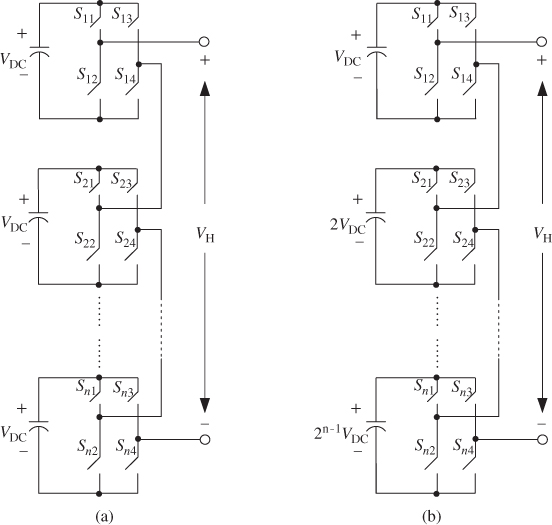
Figure 24.1 (a) Traditional CMI and (b) hybrid CMI
24.1.3 Single-Stage Inverter Topology
There are several power converter topologies employed in PV systems, characterized as two-stage or single-stage, transformer or transformer-less and with a two-level or multilevel inverter [1, 11–14]. Single-stage inverters are becoming more attractive compared with two-stage models owing to their compactness, low cost and their reliability [15]. However, the conventional inverter has to be oversized to cope with the wide PV array voltage changes, because a PV panel presents low output voltage with a wide range of variation based on irradiation and temperature, usually with a ratio of 1 : 2.
The two-stage inverter applies a boost DC–DC converter, instead of a transformer, to minimize the required KVA rating of the inverter and to boost the wide range of voltage to a constant desired value. Unfortunately, the switch in the DC–DC converter becomes the killer of the cost and efficiency of the system. For safety reasons, some PV systems have a galvanic isolation, either in the DC–DC boost converter using a high-frequency transformer, or in the AC output side of a line frequency transformer. Both of these added galvanic isolations increase the cost and size of the entire system and decrease the overall efficiency.
24.2 Quasi-Z-Source Inverter
24.2.1 Principle of the qZSI
The Z-source inverter (ZSI), as a single-stage power converter with step-up/down function, allows a wide range of PV voltages, and has been reported in applications of PV systems [16]. It can handle the PV DC voltage variation in a wide range without overrating the inverter and implement voltage boost and inversion simultaneously in a single power conversion stage, thus minimizing system cost, reducing component count and cost and improving reliability. Recently proposed quasi-Z-source inverters (qZSI) have some new attractive advantages more suitable for application in PV systems. This will make the PV system much simpler and cheaper because the qZSI draws a constant current from the PV panel, which means that there is no need for extra filtering capacitors. In addition, it features lower component (capacitor) rating and reduces switching ripples to the PV panels [16–23].
The output voltage of the PV panel has a wide variation related to changes of temperature and solar irradiation, which usually presents in a ratio of 1 : 2. It is impossible for the traditional voltage source inverter (VSI) to deal with this wide variation if there is neither overrating of the inverter nor the use of a DC–DC boost converter. For a common single-stage inverter, as shown in Figure 24.2(a) [24, 25], which is used in conventional PV systems to interface the PV array with the utility and/or load, the minimum PV DC voltage should be two times the peak value of the AC phase voltage, or 2vln. Therefore, considering a PV voltage change range of 1 : 2, the PV array has to produce 2vln to 4vln to feed the inverter. Consequently, the inverter should be designed to block four times the peak value of the AC phase voltage, or 4vln. For example, the VSI needs a minimum 340 V DC to produce 208 V AC phase-to-phase voltage for a three-phase system, and the PV voltage has to be 340–680 V considering it changes in a 1 : 2 range. Consequently, 1200 V insulated gate bipolar transistors (IGBTs) are required and the inverter is thereby two times overrated. To overcome this problem, the DC–DC boost circuit is employed, as shown in Figure 1.1(b) [26–31] and 600 V IGBTs can be used for the system. However, the cost will increase and the efficiency will be reduced.
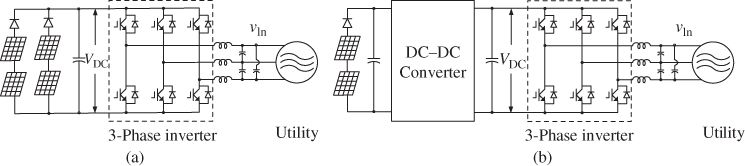
Figure 24.2 Traditional typical configuration of PV system: (a) single-stage VSI and (b) two-stage VSI
Compared with the configuration of the VSI plus DC–DC boost, the ZSI-based PV system minimizes switching devices, has lower cost and higher reliability [19, 32]. Recently, our group published a class of qZSIs with some new advantages [16, 33], which was from the original ZSI [19]. By using this new quasi-Z source topology, the inverter of a PV system becomes much simpler and its cost can be reduced. This is because the proposed qZSI draws a constant current from the PV panel; thus, there is no need for extra filtering capacitors, and it features lower component (capacitor) rating and reduces switching ripples to the PV panel [17].
Figure 24.3(a and b) shows the traditional voltage-fed ZSI and the recently proposed voltage-fed qZSI, respectively. In the same manner as the conventional ZSI, the qZSI has two general types of operational states at the DC side: the non-shoot-through state (i.e., the six active states and two conventional zero states), and the shoot-through state (i.e., both switches in at least one phase conduct simultaneously). In the non-shoot-through state, the inverter bridge, viewed from the DC side, is equivalent to a current source, whereas in the shoot-through state, the inverter bridge is a short circuit. The equivalent circuits of the two states are shown in Figure 24.4(a and b), respectively. It is well known that the shoot-through state is strictly forbidden in the traditional VSI, because it will cause a short circuit of the voltage source and damage the devices. In the qZSI and ZSI, however, the unique LC and diode network, connected to the inverter bridge, modify the operation of the circuit, allowing the shoot-through states. Furthermore, by using the shoot-through state, the (quasi-) Z-source network boosts the DC-link voltage. This feature will effectively protect the circuit from damage; thus, it improves system reliability significantly. Because of the input inductor L1, the qZSI draws a continuous constant DC current from the DC source. Compared with the ZSI that draws a discontinuous current, the constant current will reduce significantly the input stress; thus, the qZSI is especially well suited for PV system applications [17].
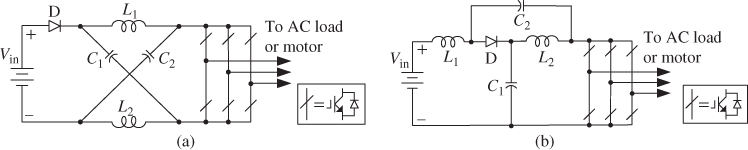
Figure 24.3 Topology of the voltage-fed ZSI and qZSI: (a) voltage-fed ZSI and (b) voltage-fed qZSI
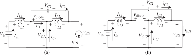
Figure 24.4 Equivalent circuit of the qZSI: (a) non-shoot-through state and (b) shoot-through state
Assuming that during one switching cycle T, the interval of the shoot-through state is T0, then the interval of non-shoot-through state is T1; thus, T = T0 + T1 and the shoot-through duty ratio D = T0/T. From Figure 24.4(a), during the interval of the non-shoot-through state T1, there are
From Figure 24.4(b), during the interval of the shoot-through state T0, one can get
At steady state, the average voltage of the inductors over one switching cycle is zero. From Equations (24.1), (24.2), we have
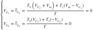
Thus,
From Equations (24.2) and (24.4), the peak DC-link voltage across the inverter bridge is
where B is the boost factor of the qZSI.
The average currents of the inductors L1 and L2 can be calculated by the system power rating P
According to Kirchhoff's current law and (24.6), we also can get that
In summary, the voltage and current stress of the qZSI are shown in Table 24.1, where
- M is the modulation index; vln is the AC peak phase voltage;
- (2)

The stress on the ZSI is shown as well for comparison.
Table 24.1 Voltage and average current of the qZSI and ZSI network
| vln | ||||||||||||
| ZSI | 0 | 0 | ||||||||||
| qZSI | 0 | 0 | ||||||||||
From Table 24.1 we can establish that the qZSI inherits all the advantages of the ZSI. It can buck or boost a voltage, cope with a wide range of input voltages and produce a desired voltage for the load or connection to the grid in a single stage. This feature results in the reduced number of switches involved in the PV system and, therefore, the reduced cost and the improved system efficiency. When the voltage of the PV panel is low, it boosts the DC-link voltage, which helps avoid redundant PV panels for higher DC voltage or unessential inverter overrating. As mentioned, it is able to handle the shoot-through state; therefore, it is more reliable than conventional VSI. For the same reason, there is no need to add any dead time into the control schemes, which reduces the output distortion.
In addition, there are some unique merits of the qZSI when compared with conventional ZSI [16, 17]. The ZSI has a discontinuous input current in the boost mode, whereas the input current of the qZSI is continuous owing to the input inductor L1 and this reduces the input stress significantly; thus, it can reduce the capacitance for the output of the PV panels. The two capacitors in the ZSI sustain the same high voltage, whereas the voltage on capacitor C2 in the qZSI is lower, which allows a lower capacitor voltage rating. For the qZSI, there is a common DC rail between the source and inverter, which is easier to assemble and causes less EMI problems.
24.2.2 Control Methods of the qZSI
24.2.2.1 Buck/Boost Conversion Mode
If the inverter operates entirely in the non-shoot-through state, as shown in Figure 24.4(a), the diode will conduct and the voltage on capacitor C1 will be equal to the input voltage, whereas the voltage on capacitor C2 will be zero. Therefore, vPN = Vin and the qZSI acts as a conventional VSI:
For sinewave pulse width modulation (SPWM), ![]() and for space vector modulation (SVM),
and for space vector modulation (SVM), ![]() . Thus, when D = 0, vln is always less than
. Thus, when D = 0, vln is always less than ![]() and this is called the buck conversion mode of the qZSI.
and this is called the buck conversion mode of the qZSI.
When the qZSI operates in boost conversion mode, there are two more modulation references: ![]() and
and ![]() , in addition to the conventional three-phase references:
, in addition to the conventional three-phase references: ![]() ,
, ![]() and
and ![]() . As shown in Figure 24.5, by replacing parts or all of the two conventional zero states with shoot-through states, the non-shoot-through states and shoot-through states will alternate in one switching cycle. Then, the peak DC-link voltage vPN can be boosted by a factor of B; its value is dependent on the shoot-through duty ratio, as defined in Equation (24.5). Notice that the six active states are unchanged and the peak AC voltage becomes
. As shown in Figure 24.5, by replacing parts or all of the two conventional zero states with shoot-through states, the non-shoot-through states and shoot-through states will alternate in one switching cycle. Then, the peak DC-link voltage vPN can be boosted by a factor of B; its value is dependent on the shoot-through duty ratio, as defined in Equation (24.5). Notice that the six active states are unchanged and the peak AC voltage becomes
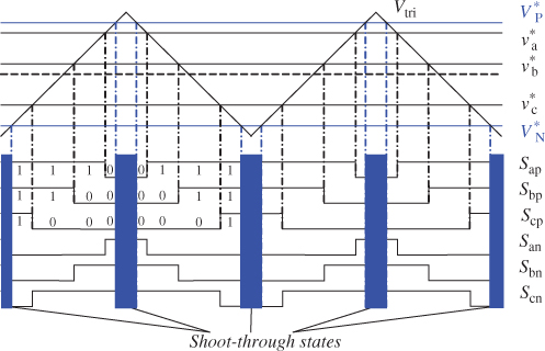
Figure 24.5 SPWM for the qZSI in boost conversion mode
24.2.2.2 Boost Control Methods
All the boost control methods that have been explored for the traditional ZSI, such as simple boost, maximum boost, maximum constant boost, as shown in Figure 24.6 [19, 20, 34], can be applied to the qZSI. It is noticeable that the voltage gain of the qZSI is G = MB, whereas the voltage stress across the inverter bridge is BVin. In order to maximize the voltage gain and to minimize the voltage stress on the inverter bridge, one needs to decrease the boost factor B and increase the modulation index M as much as possible.
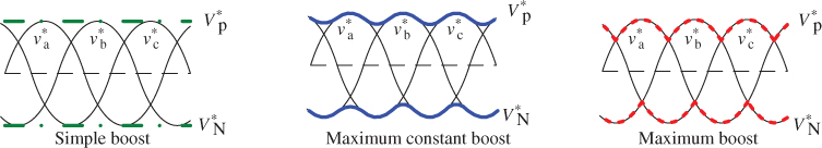
Figure 24.6 Three boost control methods with different  and
and 
Figure 24.7 shows the voltage gain versus the modulation index of three boost control methods. All present significantly higher gain than traditional VSI. Among the three boost control methods, the maximum boost control best exploits the conventional zero states; therefore, it has the maximum M and the minimum voltage stress across the inverter bridge with the same voltage gain. However, it has the drawback of low-frequency ripples on the passive components of the qZSI, which requires a larger volume and weight and greater cost of the inductor and capacitor in the qZSI network. The simple boost control has shoot-through states that are spread evenly; thus, it does not involve low-frequency ripples associated with output frequency, but its voltage stress is the largest for a given voltage gain. The maximum constant boost control is a compromise between the other two.
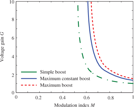
Figure 24.7 Voltage gain versus modulation index
When the third-harmonic injection is combined into the maximum constant boost control, the maximum modulation index can be ![]() , and there is lower voltage stress on the inverter bridge. With this method, the shoot-through states are introduced into the switching cycle when the carrier is either greater than
, and there is lower voltage stress on the inverter bridge. With this method, the shoot-through states are introduced into the switching cycle when the carrier is either greater than ![]() or less than
or less than ![]() , which is spread evenly in each switching cycle. Thus, the qZSI network does not involve low-frequency ripples and the shoot-through duty ratio is
, which is spread evenly in each switching cycle. Thus, the qZSI network does not involve low-frequency ripples and the shoot-through duty ratio is
the boost factor is
and the voltage gain is equal to
The peak AC phase voltage can be calculated by
24.2.3 qZSI with Battery for PV Systems
Power generated by the solar panel depends on the solar power incident on the panel, the panel temperature and the operating panel voltage. The first two factors are unpredictable because of the weather and seasons. The resultant power of stochastic fluctuations will have a negative effect on the grid. To date, there have been no significant net failures driven by these stochastic fluctuations. Nevertheless, the growing number of solar power plants is forcing us to invent and implement new solutions for this problem. Apart from investments in the extension of the grid and power capacity, as well as selective shutdown of PV systems, the integration of electricity storage systems is a more innovative idea, because the balancing difference between the forecast and real values could minimize this negative effect [35].
In addition, power consumption also presents some characteristics of season and human living habits. In spring and autumn, there are relatively more fine days with a lot of solar irradiation compared with the other seasons. These seasons also have good weather; thus, electric loads such as air conditioners may be used less often. Consequently, increased generation from PV systems and reduced loads cause a voltage rise on a power distribution line. Over weekends, during which the PV systems continue to produce the same amount of power and industrial loads are light, the grid voltage and frequency could easily become high [36]. Overvoltage may exceed the upper tolerance limit at the point of common coupling; usually, a grid overvoltage protection will regulate the output power of the PV system if the AC voltage exceeds the control range. As a result, a significant amount of possible energy will be lost in a clear day. An energy storage unit installed in each PV system can be used for voltage rise avoidance, through charging the excess electric power to the energy storage unit instead of feeding it to the grid. The energy storage unit is similar to an energy buffer, which could be charged using the differential power between the PV power and the output power to the grid, and could maximize the level of power transfer from the PV array through the MPPT, resulting in very high efficiency [4]. In addition, PV-grid-connected plants could become more reliable by acquiring the possibility to cope with some important auxiliary services [35]. There is typically a configuration available for this application, shown in Figure 24.8, when the conventional VSI is connected to the grid and/or load, and where a bidirectional DC–DC converter is used to control the battery state of charge (SOC). It is obvious that the DC–DC converter increases both the cost and the system complexity, and reduces reliability and efficiency.
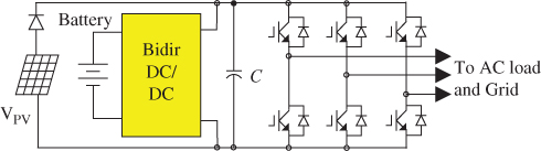
Figure 24.8 Traditional scheme
The qZSI has two independent control freedoms: shoot-through duty ratio and modulation index, providing the ability to produce any desired output AC voltage to the grid. It can regulate the battery SOC and control the PV panel output power (or voltage) simultaneously. Second, the qZSI provides the same features of a DC–DC boosted inverter (i.e., buck/boost), yet its single stage is less complex and more cost effective. Third, the qZSI has the benefit of enhanced reliability because momentary shoot-through can no longer destroy the inverter (i.e., both devices of a phase leg can be on for a significant period of time). Furthermore, our proposal includes energy storage (battery) in the qZSI for PV systems without the additional DC–DC converter, as shown in Figure 24.9. This innovative feature can reduce cost and system complexity further and is explained in detail in the next section.
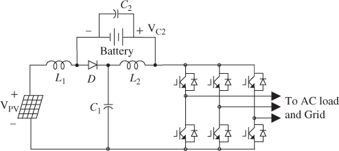
Figure 24.9 Configuration of the qZSI with battery pack for PV system
In the system of Figure 24.9, there are three power sources/consumers: the PV panels, battery and the grid/load. As long as we can control the power flow of two of them, the third element automatically matches the power difference. From Equation (24.4) of qZSI, the relationship between the capacitor-C2 voltage and the voltage of the PV panel is
where D is the shoot-through duty ratio.
In Figure 24.9, the battery voltage Vb, equals voltage ![]() of capacitor C2. The output voltage of a battery is relatively less current dependent because of the much smaller internal resistance. The voltage of a battery changes with the SOC of the battery and will be relatively constant at a certain SOC, and the voltage of the PV panel is highly current dependent; therefore, for a given battery voltage Vb, the voltage of the PV panel is controlled to be
of capacitor C2. The output voltage of a battery is relatively less current dependent because of the much smaller internal resistance. The voltage of a battery changes with the SOC of the battery and will be relatively constant at a certain SOC, and the voltage of the PV panel is highly current dependent; therefore, for a given battery voltage Vb, the voltage of the PV panel is controlled to be
At the same time, the output power of qZSI can be controlled by manipulating the modulation index to produce the desired output voltage. The output peak phase voltage of the inverter is
where M is the modulation index based on the reference waveform and the triangular waveform.
The output power to the grid can be expressed as
where I is the rms current to the grid and pf is the power factor.
Therefore, the system is able to control the output power of the PV panels and the power injected to the grid at the same time; thus, their difference is the power charging the battery.
In summary, the power of the PV panels is controlled by the shoot-through duty ratio of the qZSI; the output power to the grid is controlled by the output voltage and the current related to the modulation signal. If output power to the grid is higher than the power of the PV panels, the battery is discharged. If the output power to the grid is lower than the power of the PV panels, the battery is charged. If the SOC of the battery becomes too low, the PV panels will provide power to recharge the battery. However, the battery can only be charged when it is not fully charged already.
Let us explain this principle using examples. Case 1: for a fixed level of solar irradiance and for a fixed temperature, if the PV panel maintains a maximum output power, the power and voltage of the PV panels will be constant. When power to the grid equals the power of the PV panels, as one would expect, the battery SOC should remain constant with zero average power to the battery. When power to the grid increases to be greater than the power of the PV panels, the battery should supply the additional power requested by the grid; thus, the battery SOC will decrease. When injected grid power falls below the power of the PV panels, the additional power of the PV panel will charge the battery, increasing the SOC. (2) Case 2: Power to the grid is kept constant and the power of the PV panels changes because of the variation in solar irradiance. Again, the battery SOC should remain constant while power to the grid matches that of the PV panels. The battery will be charged when the power of the PV panels increases to be greater than the power supplied to the grid, increasing the battery SOC. When the power of the PV panels falls below the power to the grid, the battery will supply the additional power requested by the grid, decreasing the battery SOC.
24.3 qZSI-Based Cascade Multilevel PV System
24.3.1 Working Principle
In grid-connected systems, the panels are usually arranged in strings (series connection) for the required power and voltage levels, where all panels of the string drive the same current. Generally, it is preferable to use the same panels and to keep them away from any shading. However, in residential installations, it is not easy to avoid shading because of the change in sunlight direction throughout the day. Furthermore, obstacles, such as trees, birds and other constructions, can cause partial shading. Some studies have revealed that minor shading can cause a major reduction in solar power output of a PV array [37]. When a panel is shaded, it generates less optical current, and when connected in series with other panels there is a downgrading of system energy yield, because the low level of current also flows through the non-shaded panels instead of the intrinsic high current [38]. This requires the use of bypass diodes to preserve the PV array voltage and to minimize hot-spot heating and the potential for panel failures when shaded [5, 8, 37]. Figure 24.10(a) shows the I–V characteristics of two panels under different irradiance levels, and Figure 24.10(b) shows the P–V and I–V characteristics of a PV string consisting of two panels with a bypass diode incorporated. The shaded panel becomes short-circuited and the current in the string is that of the non-shaded module, because the bypass diode in parallel with the shaded panel goes into the on state. In this way, the string-generated power and voltage are greater than that in the case of an array with no bypass diodes. Nevertheless, the string power versus voltage becomes a multimodal curve, as indicated in Figure 24.10(b). Its detail is explained in the following [5].
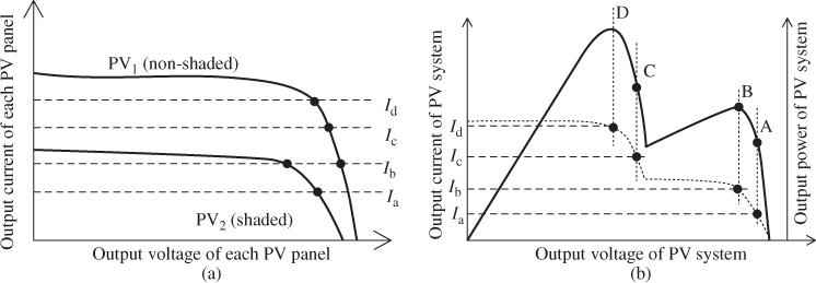
Figure 24.10 Characteristics of a small string consisting of two panels under different solar irradiance levels with the same temperature [5]: (a) current versus voltage of each panel and (b) effects of different solar irradiance levels on a string of PV arrays
When operating at point A of Figure 24.10(b), both PV panels generate power, but neither one generates maximum power. When operating at point B, the shaded module PV2 generates maximum power, but the non-shaded module does not generate maximum power. When operating at point C, the non-shaded module generates power, but the shaded module does not generate any power, because the string current flows through its bypass diode. When operating at point D, the non-shaded module generates its maximum power, but the shaded module does not generate any power because the string current flows through its bypass diode. Finally, in the case of both mismatching conditions and the presence of the module bypass diodes, the P–V characteristic curve is a multimodal curve with a number of peaks. The presence of more than one peak in the P–V characteristic of a PV string makes it difficult to implement the absolute maximum power of the PV string. Furthermore, for this case, the maximum output power of the PV string is less than the sum of the maximum generation power of all PV panels. In addition, the reduction of the string voltage at the MPP may not be acceptable according to the system specifications [8].
Reference [37] reported that the shaded panel contributes a 14.06% power loss, and an additional 11.57% loss results from the reduced MPP when the two panels are connected in series. When three or more panels are series-connected, the situation is even worse. The shading condition could be more complicated in practical PV applications, such as more than one shaded panel, making it more difficult to perform MPPT. It is of practical relevance to investigate the possibility of finding a technical and cost-effective solution to such a problem.
If independent control of each panel is possible, to allow different currents and voltages for all panels, the total generated power and voltage will be improved significantly. DMPPT is the best method for this purpose, and it comprises two major schemes. One is to use PV AC-module inverters avoiding the series-connection of panels. When a panel gets shaded, only that inverter will yield lower power, whereas the others continue to perform at their optimum level with their own inverters [38]. However, the conventional two-level inverter outputs LV because of its step-down-only operation and the low input voltage of each panel. It is necessary to step up the voltage suitably for grid connection, by using a low-frequency transformer between the inverter output and the grid, or by a DC–DC boost converter between the PV panel and the inverter input. Both of these configurations will be more costly because of the increased number of devices, and because power losses increase because of adding the DC–DC converter or transformer. Another scheme employs a multilevel inverter to replace its two-level counterpart. In this case, each PV panel is used as a separate power supply for each module of the multilevel inverter [2–4, 8, 39], and the generation point of each PV module can be controlled independently and maximized, that is, the so-called DMPPT, particularly with partial shade covering the PV facility or in the case of the mismatched PV panels. In addition to being able to maximize the power obtained from the PV panels, the multilevel inverter usually presents the advantages of reducing the device voltage stress, being more efficient, generating output AC-voltage with negligible total harmonics and allowing one to operate without transformers to step up the voltage. Among multilevel inverters, the cascade H-bridge inverter is most popular. It uses relatively few power devices and each H-bridge works at very low switching frequency. This offers the possibility of working in high power with low-speed switches and generating low-switching frequency losses, which allows working with a power range similar to the common central inverter topology, but extracting energy in a more efficient way [4].
In our proposal, the qZSI module, shown in Figure 24.9, is used to build the cascade H-bridge inverter as a practical implementation of the aforementioned DMPPT technique. Figure 24.11 presents the proposed three-phase inverter connected directly to the grid. Each phase consists of n qZSI modules, and phases B and C have the same structure as phase A. Normally, this architecture makes each module deliver the same power; however, sometimes this is not so when the output voltages of the qZSI modules are different, even though they have the same rms value of current, which depends on the modulation techniques. However, to extract the instantaneous maximum power from each panel, regardless of the solar irradiance and temperature levels, is the most important goal. The power generated by the PV panel may change owing to variations of solar irradiance and temperature levels, for instance, between summer and winter, a clear day and cloudy day, partial shading and so on. For each module, the stochastic fluctuation of solar power is inconsistent with the desired stable power injected to the grid when using MPPT. The gap between them can be compensated for by inclusion of a battery pack in each qZSI module. This topology allows independent control of the power delivered by each module. The battery pack can charge and discharge to balance the power to the grid. With the DMPPT, power generation of each PV panel is maximized even in the presence of PV panel mismatching conditions, such as supposing the non-shaded, mid-shaded and high-shaded panels of respective modules A1, A2 and An, as shown in Figure 24.11. Each qZSI module contributes to low cost, high efficiency, and reliability and is adaptive to the wide voltage variation range of the PV panel with its special voltage step-up/step-down function in a single-stage power conversion.
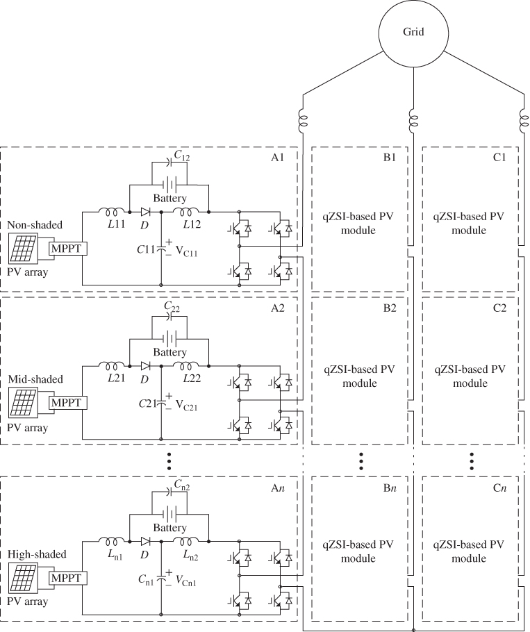
Figure 24.11 qZSI-based cascade multilevel PV power generation system
Control of the proposed PV system in Figure 24.11 will take into account the multilevel modulation, independent MPPT of each qZSI module, SOC of the battery pack and the power demand of the grid. There are 3n independent shoot-through duty ratios to control 3n qZSI modules operating at their own MPPs. The multilevel synthesis is achieved by means of a phase-shift displacement of the carrier waves of the different modules [40], and the shoot-through duty ratio should be combined into the multilevel PWM to form the final driving pulses for all switches. The power demand of the grid is achieved by multilevel modulation. The differential power between the generated maximum power of the PV panels and the power injected to the grid will charge or discharge the battery pack. The battery SOC of each qZSI module should be monitored during operation and controlled by adjusting the injected power of the grid to maintain the battery SOC within the designed range.
Parameter design of the inductors, capacitors, battery pack and operating voltage of the inverter and modules is a critical step. The optimization of these parameters will be the object of our investigation. The control of each module is elaborated, not only for its own goal but also for the entire PV system.
For the qZS H-bridge legs, the shoot-through zero state does not affect the output voltage, which will not cause harmonic content in the load current. However, the 2ω (ω is fundamental frequency of the grid) voltage ripples are a problem common in the DC-link bus of both traditional H-bridge CMIs and ZS/qZS H-bridge CMIs because the 2ω reactive power flows through each module. For the qZS H-bridge CMI, a small LC filter is sufficient when connected to the grid because the multilevel output voltage is highly sinusoidal. If using the traditional boost converter + H-bridge in the CMI, then the 2ω voltage ripples are still in the DC-link bus. Furthermore, additional switches are needed. The energy storage will require extra circuits for the traditional boost converter VFI system.
24.3.2 Control Strategies and Grid Synchronization
An electrical grid system is complex and dynamic, and is affected by many factors and disturbances. Higher penetration of renewable energy sources is leading to requirements, imposed on power converters that feed the electrical grid system, which are more stringent. Several control strategies are applied to power converters connected to the electrical grid system: voltage-oriented control (VOC), model-predictive control (MPC), direct-power control (DPC), model-predictive direct-power control (MPDPC), direct-power control with space-vector modulation (DPC-SVM) and a control method based on virtual flux (VF) [41–56]. For the VOC and DPC-SVM methods, several modifications have been developed and are reported to involve a change in the voltage modulator to allow the use of multilevel converters. Virtual flux-oriented control (VFOC) for a grid-side PWM rectifier is based on coordinate transformations between stationary α–β and synchronous rotating d–q reference systems [41, 42]. This strategy offers fast dynamic responses and a precise, steady-state performance through internal current control loops. Consequently, the final configuration and performance of the system depends largely on the quality of the applied current-control strategy. The simplest technique is hysteresis current control, which provides a fast dynamic response, good accuracy, no DC offset and high robustness. However, the major problem of hysteresis control is the variable switching frequency of the power converter. This makes the switching pattern uneven and random, which results in additional stress on the switching devices and difficulties for the filter design. Therefore, in the literature, several strategies have been reported for improving the performance of current control [41, 43]. Among the several current regulators with constant switching frequency, the most widely used scheme for high-performance current control is the d–q synchronous controller, where the currents being regulated are DC quantities and where it is easy to eliminate steady-state error and offset. DPC is a popular technique employed in grid-connected converters. By selecting appropriate switching states of the power converter, it is possible to control directly the active and reactive powers [44–49]. The technique is similar to the direct torque control, where the optimal switching state is selected by using lookup tables and hysteresis bounds. DPC using the predictive approach is also applied to the active rectifier [54, 55]. MPDPC is an extension of DPC, where the switching lookup table is replaced by an online optimization stage [56]. MPDPC achieves optimal performance by minimizing the switching losses of the converter, while controlling the output of the real and reactive powers.
Hence, the basic and advanced control features should be incorporated for any proper solution. The control technique employed should ensure stability in case of a large grid-impedance change, and be able to ride through during disturbance of the grid voltage. DC-link voltage control, adaptation to the grid voltage variation and grid synchronization, preferably with unity power factor operation, should also be incorporated. The MPPT strategy, and anti-islanding (as required by IEEE 1574), should be analyzed, although the monitoring and protection features need to be developed. Other control features are active and reactive power control, harmonic compensation, local voltage control and fault-tolerant operation during converter and grid faults. In addition, a battery energy management system is supposed to be developed and is taken into account in the control system.
24.4 Hardware Implementation
24.4.1 Impedance Parameters
The parameters of the impedance network are one of the important issues for the proper operation of the system. Several works have contributed to pursuing suitable Z-source parameters [17, 57–59]. A design process of a grid-tie PV system isillustrated in the following, according to the grid standard of Qatar.
The desired operating parameters of the converter are presented in Table 24.2. The qZS-CMI system is an 18 kW/7-level cascaded inverter, that is, threecascaded layers with 2 kW for each cell. The input DC voltage ranges from 60 to 120 V (the maximum variation of 1 : 2 is chosen because of the voltage variations of the PV panels).
Table 24.2 Desired operating parameters
| Parameters | Value |
| Maximum PV array voltage, vPV,max | 120 V |
| Minimum PV array voltage, vPV,min | 60 V |
| Rated power of each qZS-HBI, Pmax | 2 kW |
| Grid voltage | 230 V |
| Grid frequency | 50 Hz |
| Carrier frequency, fc | 2 kHz |
| Desired peak-to-peak current ripple through the qZS inductors, ri% | 20% |
| Desired voltage ripple of the qZS capacitors, rv% | 1% |
Each of the quasi-Z-source networks is a combination of two inductors: L1 and L2 and two capacitors: C1 and C2. As the equivalent circuit shown in Figure 24.4, in shoot-through states, the PV panel and qZS capacitors charge the inductors; in non-shoot-through states, the PV panel and inductors charge the loads and capacitors. Figure 24.12 shows the corresponding charge and discharge waveforms of inductor L1, L2 current and capacitor C1 voltage as an example. The voltage of capacitor C2 is the same; only the steady-state values are different from capacitor C1. In the figure, t1 is the time interval of active states and tsh is the shoot-through time interval, which is equal to (DTs/nsh). Note that nsh is the section of divided shoot-through duty ratio in each control period. It is four for the designed space-vector modulation and two for the PSSPWM. It can be seen that the purpose of the inductors is to limit the high-frequency current ripple to ri% of the maximum inductor current during shoot-through states.
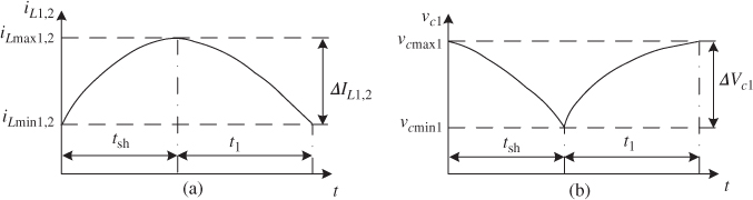
Figure 24.12 Waveforms of (a) inductor current and (b) capacitor voltage
The selection of devices is performed for the worst case, operating with rated power when the PV array voltage is a minimum and all the cascaded qZS-HBI cells have the same working condition. In this scenario, the shoot-through duty cycle reaches its maximum, and the boost ratio of the PV panel voltage is also maximal. With the maximum modulation index Mmax, the required minimum DC-link voltage vDC for each cell is
where vg with “∧” is the amplitude of the grid voltage and n is the number of cascaded cells. The maximum required voltage gain G of the qZSI can be determined by
Then, the minimum modulation index Mmin, maximum shoot-through duty ratio D and boost factor B can be determined by
To avoid the discontinuous conduction mode of the inductor, even at the worst operation point, the inductance can be calculated by
In the meantime, in non-shoot-through states, two capacitors are in series in the qZSI network. They absorb the current ripple and limit the high-frequency voltage ripple on the inverter bridge to rv% of the maximum DC-link voltage, in order to keep the output voltage sinusoidal. Therefore, the capacitance can be obtained as
According to the desired operating parameters listed in Table 24.2 and the commercialized components in the market, the qZS inductance and capacitance can be selected.
24.4.2 Control System
The proposed qZS-CMI topology with battery for PV power conversion, which is connected directly to the grid without transformers, has very limited output LC filters. Each phase consists of a series of cascaded qZSI PV modules to reach the grid levels. The qZSI PV modules comprise a group of PV panels and a qZSI with distributed MPPT for maximum energy production, boost, DC–AC inversion, and energy storage, all existing in this one single-stage power conversion unit. The gate drivers, sensors, protection and control platform based on a field programmable gate array (FPGA) or a DSP, and instrumentation circuits, will need to be designed and tested. Then, the entire power converter and PV system can be fabricated and implemented. Sensors will be calibrated and the control algorithms programmed and implemented.
The generic control structure of the proposed overall system is presented in Figure 24.13. The basic functionalities of the PV power system control are illustrated with a block diagram. The basic and advanced control features will be incorporated in the proposed solution. A number of features are required of the control technique employed: (1) ensure stability in case of a large grid-impedance change, (2) be able to ride through during disturbance of the grid voltage, (3) DC-link voltage control, (4) adaptation to grid voltage variation and grid synchronization with unity power factor operation, (5) the MPPT strategy, (6) anti-islanding, as required by IEEE 1574 the monitoring and (7) protection features. Other control features are active and reactive power control, harmonic compensation, local voltage control and fault-tolerant operation during converter and grid faults. In addition, a battery energy management system is required.
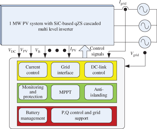
Figure 24.13 Control function diagram of the PV system
With the batteries, each module in the system can output any assigned power no matter what the PV string's MPP, because the power difference can be balanced by the connected battery through charging and discharging. As a result, all modules output balanced power and all three phases feed the balanced power to the grid.
Acknowledgments
This chapter was made possible by NPRP Grant No. 09-233-2-096 and NPRP-EP Grant No. X-033-2-007 from the Qatar National Research Fund (a member of Qatar Foundation). The statements made herein are solely the responsibility of the authors.
References
- 1. Busquets-Monge, S., Rocabert, J., Rodríguez, P. et al. (2008) Multilevel diode-clamped converter for photovoltaic generators with independent voltage control of each solar array. IEEE Transactions on Industrial Electronics, 55 (7), 2713–2723.
- 2. Kerekes, T., Teodorescu, R., Liserre, M. et al. (2009) Evaluation of three-phase transformerless photovoltaic inverter topologies. IEEE Transactions on Power Electronics, 24 (9), 2202–2211.
- 3. Negroni, J.J., Guinjoan, F., Meza, C. et al. (2006) Energy-sampled data modeling of a cascade H-bridge multilevel converter for grid-connected pv systems. 10th IEEE International Power Electronics Congress, Puebla, October 16–18, 2006, pp. 1–6.
- 4. Flores, P., Dixon, J., Ortúzar, M. et al. (2009) Static var compensator and active power filter with power injection capability, using 27-level inverters and photovoltaic cells. IEEE Transactions on Industrial Electronics, 56 (1), 130–138.
- 5. Carbone, R. (2009) Grid-connected photovoltaic systems with energy storage. Proceedings of International Conference on Clean Electrical Power, Capri, Italy, June 9–11, 2009, pp. 760–767.
- 6. Femia, N., Lisi, G., Petrone, G. et al. (2008) Distributed maximum power point tracking of photovoltaic arrays: novel approach and system analysis. IEEE Transactions on Industrial Electronics, 55 (7), 2610–2621.
- 7. Shimizu, T., Hashimoto, O., and Kimura, G. (2003) A novel high-performance utility-interactive photovoltaic inverter system. IEEE Transactions on Power Electronics, 18 (2), 704–711.
- 8. Busquets-Monge, S., Rocabert, J., Rodríguez, P. et al. (2008) Multilevel diode-clamped converter for photovoltaic generators with independent voltage control of each solar array. IEEE Transactions on Industrial Electronics, 55 (7), 2713–2723.
- 9. Negroni, J.J., Guinjoan, F., Meza, C. et al. (2006) Energy-sampled data modeling of a cascade H-bridge multilevel converter for grid-connected PV systems. 10th IEEE International Power Electronics Congress, Puebla, October 16–18, 2006, pp. 1–6.
- 10. Patel, H. and Agarwal, V. (2009) A single-stage single-phase transformer-less doubly grounded grid-connected PV interface. IEEE Transactions on Energy Conversion, 24 (1), 93–101.
- 11. Brando, G., Dannier, A., Del Pizzo, A., and Rizzo, R. (2010) A high performance control technique of power electronic transformers in medium voltage grid-connected PV plants. Proceedings of the XIX International Conference on Electrical Machines – ICEM 2010, Rome, Italy.
- 12. Lee, J., Min, B., Kim, T. et al. (2011) High efficiency grid-connected multi string PV PCS using H-bridge multi-level topology. Proceedings of the 8th International Conference on Power Electronics – ECCE Asia, ShillaJeju, Korea, May 30–June 3, 2011, pp. 2557–2560.
- 13. Xiao, B., Filho, F., and Tolbert, L.M. (2011) Single-phase cascaded H-bridge multilevel inverter with non-active power compensation for grid-connected photovoltaic generators. ECCE2011, Phoenix, AZ, September 17–22, 2011, pp. 2733–2737.
- 14. Lu, X., Sun, K., Ma, Y. et al. (2009) High efficiency hybrid cascade inverter for photovoltaic generation. TENCON 2009, pp. 1–6.
- 15. Dehbonei, H., Lee, S.R., and Nehrir, H. (2009) Direct energy transfer for high efficiency photovoltaic energy systems part I: concepts and hypothesis. IEEE Transactions on Aerospace and Electronic Systems, 45 (1), 31–45.
- 16. Anderson, J. and Peng, F.Z. (2008) A class of quasi-Z-source inverters. IEEE Industry Applications Society Annual Meeting, IAS '08, Edmonton, Alta, October 5–9, 2008, pp. 1–7.
- 17. Li, Y., Anderson, J., Peng, F.Z., and Liu, D. (2009) Quasi-Z-source inverter for photovoltaic power generation systems. Twenty-Fourth Annual IEEE Applied Power Electronics Conference and Exposition, APEC2009, Washington, DC, February 15–19, 2009, pp. 918–924.
- 18. Park, J., Kim, H., Nho, E. et al. (2009) Grid-connected PV system using a quasi-Z-source inverter. Twenty-Fourth Annual IEEE Applied Power Electronics Conference and Exposition, APEC2009, Washington, DC, February 15–19, 2009, pp. 925–929.
- 19. Peng, F.Z. (2003) Z-source inverter. IEEE Transactions on Industry Applications, 39 (2), 504–510.
- 20. Badin, R., Huang, Y., Peng, F.Z., and Kim, H.G. (2007) Grid interconnected Z-source PV system. Proceedings of IEEE PESC'07, Orlando, FL, June 2007, pp. 2328–2333.
- 21. Park, J.H., Kim, H.G., Chun, T.W. et al. (2008) A control strategy for the grid-connected PV system using a Z-source inverter. The 2nd IEEE International Conference on Power and Energy (PECon 08), Johor Baharu, Malaysia, December 1–3, 2008, pp. 948–951.
- 22. Vilathgamuwa, D.M., Gajanayake, C.J., and Loh, P.C. (2009) Modulation and control of three-phase paralleled Z-source inverters for distributed generation applications. IEEE Transactions on Energy Conversion, 24 (1), 173–183.
- 23. Xu, P., Zhang, X., Zhang, C.W. et al. (2006) Study of Z-source inverter for grid-connected PV systems. The 37th IEEE Power Electronics Specialists Conference, PESC'06, Jeju, June 18–22, 2006, pp. 1–5.
- 24. Calais, M., Myrzik, J., Spooner, T., and Agelidis, V.G. (2002) Inverters for single-phase grid connected photovoltaic systems – an overview. Proceedings of IEEE PESC'02, Vol. 4, pp. 1995–2000.
- 25. Myrzik, J. and Calais, M. (2003) String and module integrated inverters for single-phase grid connected photovoltaic systems – a review. Proceedings of IEEE Bologna PowerTech Conference, Bologna, Italy, June 2003.
- 26. Kramer, W., Chakraborty, S., Kroposki, B., and Thomas, H. (2008) Advanced Power Electronic Interfaces for Distributed Energy Systems, Part 1: Systems and Topologies. Technical Report NREL/TP-581-42672, U.S. Department of Commerce, March 2008.
- 27. Carrasco, J.M., Franquelo, L.G., Bialasiewicz, J.T. et al. (2006) Power electronics systems for the grid integration of renewable energy sources: a survey. IEEE Transactions on Industrial Electronics, 53 (4), 1002–1016.
- 28. Li, Q. and Wolfs, P. (2008) A review of the single phase photovoltaic module integrated converter topologies with three different dc link configurations. IEEE Transactions on Power Electronics, 23 (3), 1320–1333.
- 29. Asiminoaei, L., Teodorescu, R., Blaabjerg, F., and Borup, U. (2005) Implementation and test of an online embedded grid impedance estimation technique for PV inverters. IEEE Transactions on Industrial Electronics, 52 (4), 1136–1144.
- 30. Barbosa, P.G., Braga, H.A.C., do Carmo Barbosa Rodrigues, M., and Teixeira, E.C. (2006) Boost current multilevel inverter and its application on single-phase grid-connected photovoltaic systems. IEEE Transactions on Power Electronics, 21 (4), 1116–1124.
- 31. Armstrong, M., Atkinson, D.J., Johnson, C.M., and Abeyasekera, T.D. (2006) Auto-calibrating dc link current sensing technique for transformer-less, grid connected, H-bridge inverter systems. IEEE Transactions on Power Electronics, 21 (5), 1385–1396.
- 32. Peng, F.Z., Shen, M., and Qian, Z. (2005) Maximum boost control of the Z-source inverter. IEEE Transactions on Power Electronics, 20 (4), 833–838.
- 33. Anderson, J. and Peng, F.Z. (2008) Four quasi-Z-source inverters. IEEE Power Electronics Specialists Conference, PESC2008, Rhodes, Greece, June 15–19, 2008, pp. 2743–2749.
- 34. Shen, M., Wang, J., Joseph, A. et al. (2006) Constant boost control of the Z-source inverter to minimize current ripple and voltage stress. IEEE Transactions on Industry Applications, 42 (3), 770–778.
- 35. Bärwaldt, G. and Kurrat, M. (2008) Application of energy storage systems minimizing effects of fluctuating feed-in of photovoltaic systems. CIRED Seminar 2008: SmartGrids for Distribution, Frankfurt, Germany, June 23–24, 2008, pp. 1–3.
- 36. Ueda, Y., Kurokawa, K., Tanabe, T. et al. (2008) Analysis results of output power loss due to the grid voltage rise in grid-connected photovoltaic power generation systems. IEEE Transactions on Industrial Electronics, 55 (7), 2744–2751.
- 37. Xiao, W., Ozog, N., and Dunford, W.G. (2007) Topology study of photovoltaic interface for maximum power point tracking. IEEE Transactions on Industrial Electronics, 54 (3), 1696–1704.
- 38. Rodriguez, C. and Amaratunga, G.A.J. (2008) Long-lifetime power inverter for photovoltaic ac modules. IEEE Transactions on Industrial Electronics, 55 (7), 2593–2601.
- 39. Peng, F.Z., McKeever, J.W., and Adams, D.J. (1997) Cascade multilevel inverters for utility applications. The 23rd International Conference on Industrial Electronics, Control and Instrumentation, IECON97, New Orleans, LA, November 9–14, 1997, pp. 437–442.
- 40. Kanchan, R.S., Baiju, M.R., Mohapatra, K.K. et al. (2005) Space vector PWM signal generation for multilevel inverters using only the sampled amplitudes of reference phase voltages. IEE Proceedings of Electric Power Applications, 152 (2), 297–309.
- 41. Teodorescu, R., Liserre, M., and Rodriguez, P. (2011) Grid Converters for Photovoltaic and Wind Power Systems, John Wiley & Sons, Ltd.
- 42. Wu, B., Lang, Y., Zargari, N., and Kouro, S. (2011) Power Conversión and Control of Wind Energy Systems, John Wiley & Sons, Ltd.
- 43. Blaabjerg, F., Teodorescu, R., Liserre, M., and Timbus, A.V. (2006) Overview of control and grid synchronization for distributed power generation systems. IEEE Transactions on Industrial Electronics, 53 (5), 1398–1409.
- 44. Eloy-Garcia, J., Arnaltes, S., and Rodriguez-Amenedo, J.L. (2007) Extended direct power control for multilevel inverters including DC link middle point voltage control. Electric Power Applications, IET, 1 (4), 571–580.
- 45. Rivera, S., Kouro, S., Cortes, P. et al. (2010) Generalized direct power control for grid connected multilevel converters. Proceedings of IEEE International Conference on Industrial Technology (ICIT), Chile, March 14–17, 2010, pp. 1351–1358.
- 46. Malinowski, M. and Kazmierkowski, M.P. (2003) Simple direct power control of three-phase PWM rectifier using space vector modulation – a comparative study. EPE Journal, 13 (2), 28–34.
- 47. Malinowski, M., Jasiński, M., and Kazmierkowski, M.P. (2004) Simple direct power control of three-phase PWM rectifier using space-vector modulation (DPC-SVM). IEEE Transaction on Industrial Electronics, 51 (2), 447–454.
- 48. Noguchi, T., Tomiki, H., Kondo, S., and Takahashi, I. (1998) Direct power control of PWM converter without power source voltage sensors. IEEE Transaction on Industrial Electronics, 34 (3), 473–479.
- 49. Zhi, D., Xu, L., and Williams, B.W. (2009) Improved direct power control of grid connected DC/AC converter. IEEE Transaction on Industrial Electronics, 24 (5), 1280–1292.
- 50. Malinowski, M., Kazmierkowski, M.P., Hansen, S. et al. (2000) Virtual flux based direct power control of three-phase PWM rectifiers. Proceedings of IEEE Thirty-Fifth IAS Annual Meeting and World Conference on Industrial Applications of Electrical Energy, Roma, Italy, October 8–12, 2000, Vol. 4, pp. 2369–2375 (in English).
- 51. Malinowski, M., Kazmierkowski, M.P., Hansen, S. et al. (2001) Virtual flux based direct power control of three-phase PWM rectifiers. IEEE Transaction on Industry Application, 37 (4).
- 52. Serpa, L.A., Barbosa, P.M., Steimer, P.K., and Kolar, J.W. (2008) Five-level virtual-flux direct power control for the active neutral-point clamped multilevel inverter. Proceedings of the IEEE Power Electronics Specialists Conference PESC, June 15–19, 2008, pp. 1668–1674.
- 53. Antoniewicz, P. and Kazmierkowski, M.P. (2008) Virtual flux based predictive direct power control of ac/dc converters with on-line inductance estimation. IEEE Transaction on Industrial Electronics, 55 (12), 4381–4390.
- 54. Cortes, P., Rodriguez, J., Antoniewicz, P., and Kazmierkowski, M.P. (2008) Direct power control of an afe using predictive control. IEEE Transaction on Power Electronics 23 (5), pp. 2516–2523.
- 55. Cortes, P., Rodriguez, J., Antoniewicz, P., and Kazmierkowski, M.P. (2008) Direct power control of an AFE using predictive control. IEEE Transaction on Industrial Electronics, 23 (5), 2516–2523.
- 56. Geyer, T. (2010) Model predictive direct current control for multi-level converters. Proceedings of IEEE Energy Conversion Congress and Exposition, Atlanta, GA, September 2010.
- 57. Rajakaruna, S. and Jayawickrama, L. (2010) Steady-state analysis and designing impedance network of Z-source inverters. IEEE Transactions on Industrial Electronics, 57, 2483–2491.
- 58. Ellabban, O., van Mier, J., and Lataire, P. (2011) Experimental study of the shoot-through boost control methods for the Z-source inverter. EPE Journal, 21, 18–29.
- 59. Roasto, L. and Vinnikov, D. (2010) Analysis and evaluation of PWM and PSM shoot-through control methods for voltage-fed qZSI based DC/DC converters. 2010 14th International Power Electronics and Motion Control Conference (EPE/PEMC), September 6–8, 2010, pp. T3-100, T3-105.