
Chapter 18B
Real-Time Simulation of Modular Multilevel Converters (MMCs)
Luc A. Grégoire1, Jean Bélanger2, Christian Dufour2, Handy. F. Blanchette1 and Kamal Al-Haddad1
1Electrical engineering department, Ecole de Technologie Supérieure, Montréal, Canada
2OPAL-RT TECHNOLOGIES INC, Montréal, Canada
18B.1 Introduction
Real-time simulation offers several advantages to speed up the development of new product. One of these advantages being the possibility to test and develop controllers when the hardware is not yet available. This is a serious advantage in the case of high-order multilevel converter, like modular multilevel converter (MMC) topology. Its physical size could raises serious issues for most laboratories, without even mentioning the cost to build such a complex structure. It can also be useful to analyze the interaction between several MMC and conventional high-voltage DC (HVDC) systems installed on the same power grid. Furthermore, it can perform factory acceptance test of the control system before the installation in the field. Nowadays, real-time simulators are often used simply to accelerate simulations, which could take several hours for simulation runs of a few seconds with a power grid having two or three converter stations using conventional single-processor simulation software. This chapter introduces bases of real-time simulation: its advantages and its constraints. Using these bases, real-time simulation of an MMC will be undertaken. This topology was first introduced in [1], it is made of many identical cells connected in series. Its modularity makes it suitable for various applications from medium voltage in a drive system using only a few cells [2] to a large HVDC transmission system containing a wide range of cells [3, 4]. Connecting many of these cells in series reduces the voltage level that each sustains, decreasing the price of each component, reducing the switching losses and smaller dV/dt at its AC bus, while producing a sinusoidal waveform with a very low total harmonic distortion (THD) eliminating the use of bulky reactive component filter.
18B.1.1 Industrial Applications of MMCs
This topology was first tested by ABB in 1997. It consists of a 10 km overhead transmission line with a 3 MW capability at ±10 kV between Hällsjön and Grängesberg in Sweden. It was used as a proof of concept and to establish the capability of this new topology. The MMC was named HVDC light by ABB and was first used in a commercial project in Australia between Mullumbimby and Bungalora. Its voltage rating was ±80 kV with a power rating of 180 MW commissioned in 2000. Not long after, Siemens commercialized a similar topology as HVDC PLUS. Its first commercial project was a submarine HVDC link connecting San Francisco city center to a substation in the Pittsburgh area, and it was commissioned in 2010 [5].
As of today, MMC projects being built are point-to-point converters only. Though actual HVDC networks have been discussed theoretically, protection system for such network still needs to be developed. ABB announced in November 2012 that they achieved an HVDC breaker called hybrid HVDC breaker [6]. Now that it has been used in a point-to-point setup, it will be tested in HVDC grid and should soon be commercialized. These new developments could change the future of power transportation.
18B.1.2 Constraint Introduced by Real-Time Simulation of Power Electronics Converter in General
Until now, big differences still exist between what can be achieved with standard or offline simulation software and real-time simulator. The major constraint is in the time available to solve the differential equations. This describes the operation sequences of power electronic circuit. Offline simulation usually uses a precise variable-step solver. They will use two different orders of discretization, one higher than the other, and will iterate reducing the time step of every iteration until the difference between the two solutions coincides within a pre-set tolerance [7]. This process is very efficient for typical simulation of system with few disturbances. However, it can be very slow especially in power electronic where stiff system with repetitive switching of fast semiconductor needs to be solved. On the other hand, real-time simulation uses several processors, operating in parallel and fixed-step solver and has a fix period of time to solve the differential equations. If a time step of 50 µs is chosen to discretize a system, the real-time simulator has to solve the differential equation within that period. Larger model, with more state-space equations, will naturally take more time to be solved; in this case, there are very few solutions to obtain acceptable results. One can increase the chosen time step, risking instability or inaccuracy. The computing power of real-time simulator has increased over the past decade following Moore's law [8] and is suited to simulate relatively small model. However, the real-time simulation of very large power system requires to decouple the system in smaller subsystems that can be solved in parallel [9, 10]. Nowadays, most real-time simulators will achieve a time step between 10 and 50 µs when using several general-purpose processors or digital signal processors (DSPs) and between 100 ns and 1 µs when using field gate programmable array (FPGA).
In the case of power electronic or circuit that contains fast switching devices, the chosen time step is very important since it will determine the accuracy that can be achieved by the pulse-width modulation (PWM) circuit to generate the gating signals. A switching frequency of 10 kHz has a period of 100 µs. If one chooses the time step of the real-time simulator equal to 50 µs, then there is a maximum of 50% error on the time of occurrence of the switching event. Such inaccuracy may produce unrealistic transients and harmonics that could be confused with faulty controllers. This has motivated the usage of super-fast computer subsystem, where the time step can be reduced further, or an interpolation scheme in order to achieve accurate switching frequency [11]. Moreover, this is one of the reasons to justify the use of FPGA to solve such a problem and consequently increase the popularity of the technology. FPGA chips operate at a 100–400 MHz clock frequency much lower than 2–4 GHz used for the general-purpose processors. However, processors are composed of hundreds of DSP blocks operating in parallel to achieve very small time step between 100 ns and 1 ms. This goal is still not possible with the most powerful commercial computer using general-purpose processors because of the processor communication latency. Furthermore, firing signal of power devices generated from actual power electronic controller can be connected directly to FPGA digital input pins, which are connected to the model of the converter simulated in the same FPGA. The result is that the total latency between the firing order, measured at the controller output and the resulting currents computed by the FPGA model could be less than 200 ns to 1 µs. Such small time delay is acceptable for most controllers working with sampling of 10–100 µs and with PWM carrier frequency up to about 50 kHz. In such a case, the accuracy will be as good as variable-step solver. Such low latency and accuracy cannot yet be achieved using general-purpose computer because of the typical latency of the PCI communication system of 2–3 µs.
Moreover, another important parameter to be considered is the type of modeling technique chosen to discretize the circuit. The two main well-known techniques are the nodal and the state-space methods. Depending of the circuit topology, one can be more advantageous than the other. Taking shortcut and making this simpler than it actually is, time of execution in real-time simulation comes down to the size of the matrix and its sparsity; since the latter needs to be inverted each time there is a change in the circuit topology, caused by a switching event. In the case of the circuit illustrated in Figure 18B.1, a state-space approach would generate a two-by-two matrix to discretize or inverse, as shown in Equation (18B.1), since there are only two state variables. The nodal approach would yield a four-by-four matrix to solve, as shown in Equation (18B.2). This simple example illustrates the same concept that can be applied to large circuit.
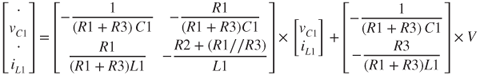
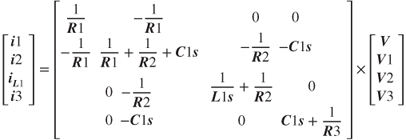
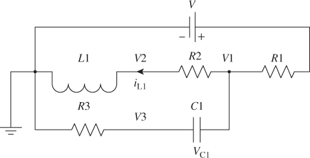
Figure 18B.1 Circuit illustrating state-space versus nodal appro!ach
Most simulation software uses one or the other method without giving the choice to the user. It is only brought up here to stay as broad and general as possible. Also when it comes to FPGA implementation, very few off-the-shelf tools are now available [12, 13]. Many users still have to develop their own FPGA model despite of its complexity and researchers are still trying to develop general-purpose electrical solvers, which would eliminate this complex task of implementing models and solvers in FPGA chip. Furthermore, one must keep in mind that one of the most difficult operations to be accomplished on FPGA is the division; therefore, it renders that inverting a matrix is an important research topic to complete it in a timely fashion suitable for a real-time simulation.
18B.1.3 MMC Topology Presentation
An MMC topology is constituted by an equal number of cells, presented in Figure 18B.2a, that are distributed in the upper and lower limb, shown in Figure 18B.2b. The cell includes switches S1, S2 and the DC-bus capacitor. When a cell is ON, the capacitor voltage is applied to its output using the upper switch S1 of the cell. When a cell is OFF, it is bypassed using the lower switch S2.
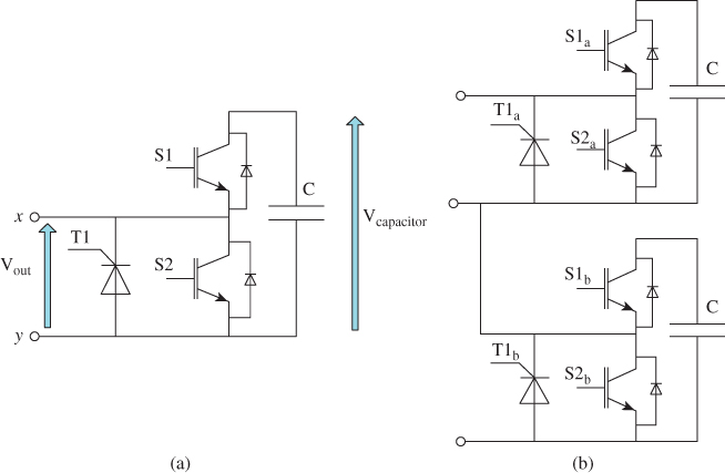
Figure 18B.2 (a) Single MMC cell with its protection and (b) MMC limb
The voltage obtained at the mid-point of the converter arm is given by the number of conducting cells in each limb. At any given time, only half of the cells from one arm are conducting. For instance, if a converter contains 100 cells, only 50 cells distributed between the upper and lower limbs of an arm are conducting at any giving time. Figure 18B.3 shows the voltage seen at mid-point in the following cases:
- 1 cell in the upper limb and 49 in the lower limb are conducting, mid-point is near HVDC+.
- 25 cells in the upper limb and 25 in the lower limb are conducting, mid-point is zero.
- 49 cells in the upper limb and 1 in the lower limb are conducting, mid-point is near HVDC.
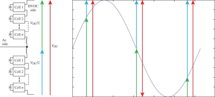
Figure 18B.3 Standard exemple of one MMC arm for HVDC link
When a cell is conducting, its voltage will vary according to the limb current. The voltage is then regulated with rigorous algorithm to choose which cell to turn ON or turn OFF. Though this topology was proposed a few years back, only the increase in the computation power of controller made it possible to accurately control it. Since then, many methods have been proposed to control this converter topology requiring individual control of each cell capacitor voltage [14–16], to cite only a few.
The number of cells plays two roles in this topology. The number of cell is linked to the quality of produced voltage. When more than 12 levels are used, it demonstrates that the gain on the THD becomes almost negligible, as shown in Figure 18B.4 [17].
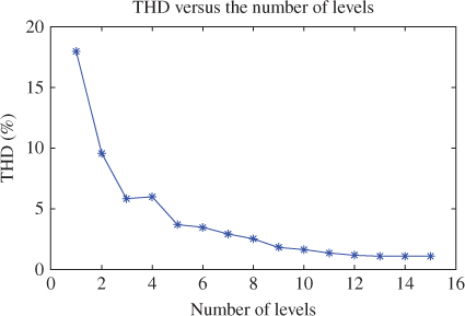
Figure 18B.4 THD versus the number of levels
In the case of MMC used for HVDC application, the extremely high number of cells used reduces the stress on each component and also offers a redundancy improving reliability. Furthermore, increasing the number of cells reduces the switching frequency of each individual cell up to once per cycle [4].
Since this topology is a voltage source converter (VSC), it has complete control on the power flow, both active and reactive. Also unlike most HVDC classic topology, it does not require a network to synchronize itself, allowing to make a black start, since the voltage is imposed by the converter. But all of these advantages come with the price of complex control law that needs to be optimized and tested.
18B.1.4 Constraints of Simulating MMCs
When it comes to real-time simulation of MMCs, there are two major problems to resolve. The first being the considerable size of the model, whether a state-space or a nodal approach is taken; and the second being the tremendous amount of input/output required to control the converter. Bear in mind that the main purpose to real-time simulation is to be interfaced with a real controller. When it comes to thousands of cells to be controlled, it can only be assumed that even more signals are required for control of the converter. Most of the processing time was due to the I/O management and data transfer between the external controller and the MMC model. It is therefore obvious that MMC simulators with 1000 cells per limb would require an I/O processing time much larger than 25 µs, which is unacceptable.
18B.1.4.1 Solving Large State-Space System
One way to surmount the first problem is to exploit certain advantages of MMC topologies. Having a rather large inductance in each limb, this generates a very “strong state” on the AC side; where the current variation is rather slow. The DC side being often connected to a DC cable, the capacitance of the cable also generates a “strong state” on the DC side, where the HVDC voltage variation is slow. There two “strong state” can be used to decouple each limb. Once decoupled, it is possible to spread the computation burden over multiple computing units achieving parallel processing. Furthermore, one limb can be divided into smaller subcircuit without any extra efforts on computation time.
18B.1.4.2 Solving I/O Management Problem
Having met the requirement to decouple large system, the only problem remaining is the one concerning the amount of I/O to be dealt with. Architecture of real-time simulator will be discussed later, but for now what need to be understood is that most real controller and simulator platforms use custom-made card with a communication link to its computation unit. More I/O implies more data to be sent over the communication link and therefore requires more time. If more time is required for I/O communication, this leaves less time for computation of the model. What have been done in the first part will actually help resolve the second issue. Spreading the model across more computation unit reduces the amount of data that each must exchange with the I/O solving the second problem. Furthermore, simulating MMC cells directly on FPGA chips, which are managing I/O channels, also minimizes data transfer between external controllers and simulator main processors. Such technique is now used by most advanced real-time simulators.
Separating the large state-space systems formed by the MMCs coupled to the AC network in order to achieve parallel processing can be achieved in several ways but might involve the use of artificial delays [18] or multirate simulation [19]. As of now, there are no formal and easy methods to achieve parallel processing of complex power electronic circuits coupled to large AC circuits.
18B.1.4.3 System-Wide Simulation Simulated Faster Than Real Time
Several studies target the behavior of several converters in a large network or the development of controllers before the manufacturing of controller prototype boards. In these cases, the controller algorithm can also be simulated in the same simulator simulating the MMC system and the grid. Consequently, no external I/O are required and it is then possible to simulate faster than real time; that is, a typical simulation run of 60 s could take 60 s with a real-time simulator or only a few seconds with a simulator running faster than the real time. In real-time simulation, the acceleration factor is 1, where the time step used and the time required to execute the model has a ratio of 1. For faster than real-time simulation, the acceleration factor is greater than 1 since the time required to solve the equation of the model is smaller than the time step used. Like before, if the model is decoupled and spread over many computation units, its acceleration factor is increased above 1 while the use of conventional signal-processor simulation software may have an acceleration factor much lower than 1, that is, the simulation time of a 10 s case could take several minutes or event hours depending on the network and MMC size. As the control development requires to analyze hundreds of contingencies and to optimize several parameters, it is obvious that fast simulation tools exploiting multicore processors and FPGAs will become essential as model complexity increases.
18B.2 Choice of Modeling for MMC and Its Limitations
As mention earlier, time is a very important constrain in real-time simulation; choosing the appropriate level of modeling for a specific application helps to reduce the required computation time. The level of modeling can be classified into three main categories namely: detailed model, switching function model and average model. Each of them will give accurate results but they all have different limitations.
18B.2.1.1 Detailed Model
There exists different level of modeling in the so-called detailed model. Most of them offer too much detail which is not useful for real-time simulation used to design, optimize and test control systems. The highest level of details could be qualified as “SPICE” modeling, where all the parasitic capacitors of the power switch and strain inductance of the PCB are taken into consideration. This type of modeling is used to calculate losses that will occur during switching. Even though this is a very important part of a real design, real-time simulation should not, but also could not, be used to evaluate switching losses and electromagnetic interference (EMI). Taking a numerical approach, the time constant of components such as picofarad and nanohenry is around nanoseconds; these types of time step cannot be achieved today in real time even with FPGA. Processor technology advancements may however make this dream possible during the next decade.
The model where the switch and diode are considered as linear components can also be considered as a detailed model. Every semiconductor is represented by an impedance: small when conducting and high when blocking. Whether a state-space approach or a nodal approach is used, a new set of matrices need to be computed and inverted each time there is a change in switch status. This approach has been demonstrated using Hypersim [20] or the State-Space Nodal (SSN) solver [21, 22] with 100 cells/arms MMC at time step in the 30 µs range.
18B.2.1.2 Switching Function
Switching functions or event-based dynamic system [23] can be interpreted as a switch case; for a certain input, certain behaviors are expected. In the case of Figure 18B.2, the switching function can take this form:
- If S1 = 1 and S2 = 0, Vout = Vcapacitor
- If S1 = 0 and S2 = 1, Vout = 0
- Else Vout = 0
This implies that the switching is complementary and that there are no conducting losses, that is, ideal switch. To introduce the switching losses, the current must be taken into account. Therefore, the switching function becomes
- If S1 = 1 and S2 = 0, Vout = Vcapacitor–Is*Ron
- If S1 = 0 and S2 = 1, Vout = 0–Is*Ron
- Else Vout = 0
The flexibility of switching function makes it a very powerful tool, but it requires a very good understanding of the circuit in order to predict and have a contingency for every possible case. Unlike detailed model, this can result into an unnatural behavior and discontinuity that is not present in real life. The gain is in the rapidity of execution, which makes it a very good candidate for real-time simulation. Also when the limitations are known, it does not prevent the use of this model in all other supported mode. In this model, the number of states is not reduced, meaning that an integrator is required for every simulated capacitor cell. A detailed example is given in Section 18.4.2.
18B.2.1.3 Average Model
The term average model here is not only intended as in the classical way. In classic average model, the duty cycle is given as input instead of PWM, but here the overall voltage of every cell's capacitor is also averaged out across all the cells, making an ideal regulation of voltage of all the cells. This type of modeling is the easiest to implement, but it is also the one offering the most limitation. The main interest of this implementation is to study the behavior of the converter in a larger network where the regulation of each cell is of little interest. Similar to the switching function, the cell output is given by a simple equation decoupling it from the large system. The rest of the system will see the converter as a variable impedance as it would be with a detailed model. Again, a detailed example of the implementation is given in Section 18.4.1.
One drawback of this modeling is that it needs a special implementation to support the high-impedance mode occurring when no pulses are applied to the converter. In this mode, the output of the converter, a voltage source, is only controlled by its current when no pulses are applied to the switches. Normally, if the voltage applied to the limb is higher than the sum of all the capacitor voltages of this limb, current should circulate through the antiparallel diode of the switches of the cells, charging the cells' capacitor to voltage applied to the input of the limb. Once all the cells are charged, the current should become zero, since the antiparallel diode is not polarized anymore, and stay at zero until either of the pulses is applied again to the converter or the antiparallel diodes are polarized. Different schemes can be used to achieve this behavior, a voltage source is controlled by a voltage, but if it is not well implemented the response of the model can become erratic.
All three different types of modeling presented here serve a specific purpose, understanding the limitation of each model helps one to determine whether or not this implementation is suited for his application.
18B.3 Hardware Technology for Real-Time Simulation
In the mid-1960s, real-time simulation was achieved using analog simulator, where real linear and nonlinear components were used to model and simulate a circuit [24]. Not long after hybrid simulators, part analog part digital, were introduced and then with the evolution in the microprocessor speed, fully digital simulators were achieved. Even though the first digital simulators were limited, their smaller size and versatility made them more attractive and their popularity was powered by the increase in computer power capability over the last 15 years. For these reasons, analog and hybrid simulators are hardly used nowadays and would not be explained further here. As for digital simulators, two main technologies divide them; the first one uses sequential programming embedded on DSP or microprocessor and the second type makes use of parallel programming on FPGA. Because of their differences and their complementarity, it is not rare to see both technologies in one simulator, taking advantage of each one of them. Their respective features are discussed in the following section.
18B.3.1 Simulation Using Sequential Programming with DSP Devices
DSP is digital signal processor optimized for certain applications. It receives sequential programming: a series of instructions which are executed subsequently and repeated in a loop. These instructions need to be understood by the processor, what can be called low-level language. But it has to be entered by a user high-level language. The gap between those two levels is the different programming language, such as C, C++ and java. Every manufacturer has a different machine code that can only be understood by their hardware. Using a common language by the user, like C, manufacturers make compilers that are compatible with their hardware. Nowadays, high-end processor can execute billions of instructions per second. In order to achieve further more computation power, as mentioned earlier, it is possible to execute a different set of instruction in parallel using multiple processors sharing a high-speed communication link.
In real-time simulation, the most sophisticated processors are used in specially designed hardware. The code required is generated using software like Matlab/Simulink, so users do not require to bother about writing code. When multiple processors are available in parallel, users also rely on software to easily distribute the computational burden among them.
One of the greatest examples of real-time simulation in parallel is the Hypersim simulator, developed at IREQ, the engineering department of Hydro-Quebec [25]. It can simulate a large network, thousands of nodes, cluster of hundreds of CPU while the allocation of the processor unit to simulate each network subsystems is fully automated [26]. Other real-time simulator would normally require the intervention of advanced user in order to distribute the computation load over multiple computing unit [27, 28].
18B.3.2 Simulation Using Parallel Programming with FPGA Devices
FPGA offers much more flexibility when it comes to executing instructions; it actually allows user to develop its own instruction set. Logic operators like NAND-gate or XOR-gate, basic arithmetic like sum, multiplication are some of the components available. By using these functions, users can make an optimized set of instruction for a specific application. On older FPGA generation, only fixed-point representation was available, but since 2009, built-in operators supporting floating point are now available.
In FPGA implementation, signals travel as fast as their propagation allows. The number of operations that can be done will depend on the design; the route that signals need to take for a desired logic. On FPGA, clock signals are used to ensure that the expected result has reached its destination and is synchronized with other signals. Figure 18B.5 shows the concept of propagation to a simple circuit and the synchronization of its output.
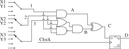
Figure 18B.5 Example of logic propagation
From Figure 18B.5, since only one level of logic gate is required to obtain A, it can be supposed that it will be ready before B that needs two levels of logic. C might change when A is ready and change again when B is ready. To avoid uncertain value at the output, a register is added and synchronized with a clock signal. By doing so, D will be synchronized with the clock and its value will be accurate as long as the period of the clock is long enough for the inputs 1, 2 and 3 to pass through the logic resulting into C. In Figure 18B.5, the results of A and B are being processed simultaneously and independently; this is the major advantage of FPGA referred to as parallel processing. From simple logic to large matrix multiplication can be performed in parallel and the result for the global solution is found in the end where all the different solutions are joined and synchronized.
Understanding that the process can be synchronized to a specific clock, it is also possible to use time multiplexing or pipelining, allowing the same logic to be used for different processes. If the clock of the process is slower than the clock of the FPGA, it becomes possible to execute the same process using the same logic. For example, if the process shown in Figure 18B.5 can be obtained one FPGA clock period, but its inputs are only ready be executed, then every five FPGA clock periods. By multiplexing the input, using selector and demultiplexing the output, the same logic could be used up to five times to calculate the same process. The chronogram of Figure 18B.6 shows the time multiplexing with only two different processes. Process X has inputs X1, X2 and X3; process Y has inputs Y1, Y2 and Y3; and each process, X and Y, yields the results of A, B and C in time. At every clock, the values from the different processes X and Y are applied to the logic and their results are shown on the chronogram. After the two processes, the logic is not used and its result is not important. The results of DX and DY are updated when available and stay there until the next clock of the slow process.
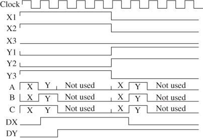
Figure 18B.6 Chronogram of time-multiplexed process
Such design can ensure that none of the resources are left idling during the different processes, but it requires very accurate synchronization and design.
The next example is more related to simulation: the implementation of a forward Euler integrator. The FGPA has a clock of 5 ns and the integrator time step is 20 ns; it is then possible to use pipelining. Figure 18B.7 shows the block schematic used in this example. The input A receives the multiplexed in time values to be integrated. B is the result of the values multiplied by the integration time step, 20 ns. D is actually the output of the sum C with a four-step delay, making the forward Euler integrator. The result in D can then be demultiplexed to send the integrated values to the right process. Here, the integration time step was chosen to facilitate the representation in a chronogram of the system in Figure 18B.8. Such a small time step is unlikely to be chosen since it would require a very high level of precision if one chooses to use a fixed-point or a floating-point representation.
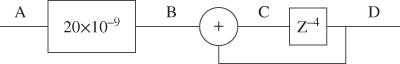
Figure 18B.7 FPGA integrator using pipelining
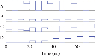
Figure 18B.8 Chronogram of pipelined integrator
The great versatility of the FPGA also creates its main drawbacks: complexity to implement models and excessive time to generate the bitstream. The example given earlier clearly demonstrates that the programming complexity is much larger than using high-level language like C++ or very high-level language like Simulink and code generators (RTW). Such complexity limits the number of specialists who can develop and maintain models. The debugging is also very difficult and long.
Because it is an FPGA, each individual gate needs to be programmed and interconnected when generating the code. With the size of FPGA and models getting larger and larger, the required time to compile the code, or bitstream, also increases. Meaning that if the configuration of your model changes, you need to recompile a new version of your bitstream, which may take several hours.
One option to avoid these two drawbacks is the use of embedded solver on the FPGA [29]. This allows testing many different circuit configurations and if needed it is also possible to make some changes and recompile a new bitstream.
18B.4 Implementation for Real-Time Simulator Using Different Approach
These are simple examples to give the reader the bases allowing him to implement its design. Matlab/Simulink was used to implement and test these implementations, but similar results could be achieved with any other simulation software. For both examples, all cells from a limb are represented by an equivalent voltage source. The only difference is in how the voltage is computed. The equivalent circuit is shown in Figure 18B.9. VUA, VUB and VUC represent the upper limb equivalent voltage, whereas VLA, VLB and VLC represent the lower limb equivalent voltage.
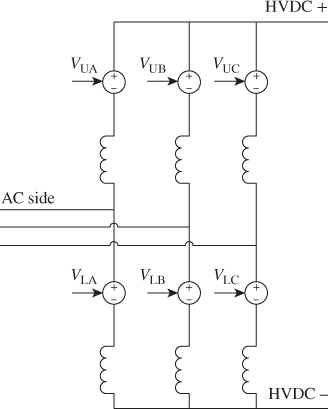
Figure 18B.9 Equivalent decoupled circuit
This method of decoupling is adequate since there are two very large states in the model; the large arm inductance ensures a slow variation of the current and the large cell capacitors ensure a slow varying voltage. Measuring the current from the arm inductance, the equivalent voltage from all the conducting cells is computed. In order to break an algebraic loop, a forward Euler integration method is used; this would not affect much the stability of the circuit since it is introduced at a point where there are dominating poles.
18B.4.1 Sequential Programming for Average Model Algorithm
This type of modeling can be used to test the inner and outer controls for converters that would be connected to a larger network. This allows estimating the load flow, verifying contingency test or general behavior of the overall network without having to bother regulating each individual capacitor cell.
For this model, the following assumptions are made:
- The current in one limb is the same for all the cells forming that limb, naturally because all are connected in series.
- All the capacitors have the same value; the integration of the current will result in the same voltage variation for all the capacitors of conducting cells.
- Only the number of conducting cells is required as input to the model, it is assumed that the choice of which cell is turned ON within a limb is made by a local and independent controller, who is not part of the model.
Figure 18B.10 shows a block diagram for one limb. It has the limb current and the number of cells ON as input, and the sum of all conducting cells' voltage as output.
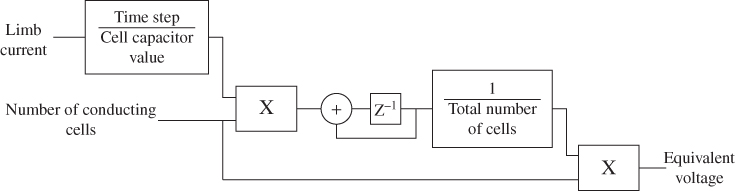
Figure 18B.10 Block diagram for average MMC model
The limb current is multiplied by the time step and it is divided by the capacitor value, giving the voltage variation of any conducting cells. Then this voltage variation is multiplied by the number of conducting cells and the result is added to the previous voltage value of all cells. The total voltage value is divided by the total number of cells obtaining the capacitor voltage of a single cell; this is how the regulation of all the cells is made to the same voltage. Finally, the voltage of a single cell is multiplied by the number of conducting cells generating the equivalent voltage for a single arm.
This technique is simple and could even be implemented in a variable-step solver with small modification. The only drawback is that natural rectification using antiparallel diodes from the cells' switches is not considered in this implementation as well as the possibility to simulate faults inside the limb and to test the individual cell voltage regulator.
Using this implementation, the HVDC grid of Figure 18B.11 was simulated faster than real-time simulation. This configuration is the DC-grid benchmark proposed by the CIGRE work group B4-57. The converter A1 is connected to a larger network, modeled by two voltage sources. Converters B1, B2 and B3 are connected to a different network but also have an AC link between one and the other. Converters C1, C2, D1 and F1 are offshore wind farm and E1 is an isolated offshore load. All the offshore converters are connected through underground cables for their HVDC link. Converters on land use overhead transmission of power lines to interconnect among them.
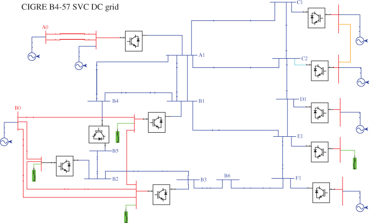
Figure 18B.11 CIGRE B4-57 HVDC grid
Figure 18B.12 shows the response at the converters C1 and C2. Only the phase A is monitored in this case, but all phases are available. In this test, there is a three-phase fault on the AC side between C1 and C2. When the fault occurs, line between C1 and C2 is opened at each end for two cycles and then it is reclosed. At this point, the fault has been cleared. Figure 18B.12 shows the voltage at each converter. On C2 side, at reclosing an overvoltage is seen. This overvoltage can vary according to the angle at which the breaker is reclosed. Using this model and a sequencer, a series of tests can be generated to make a Monte Carlo study to identify the V2% [30].
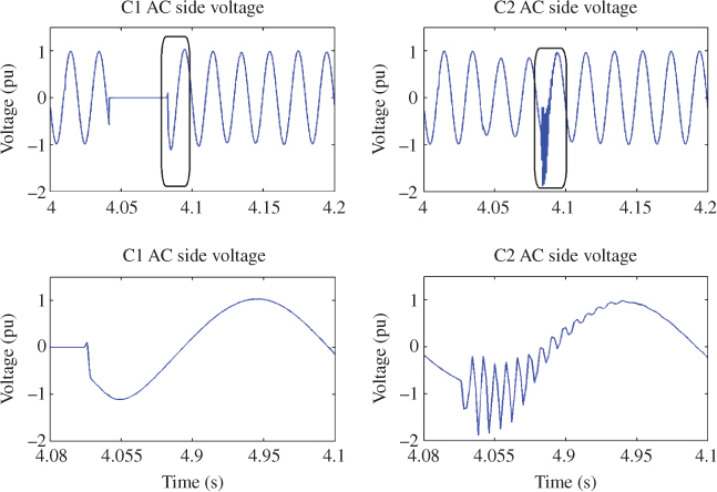
Figure 18B.12 CIGRE benchmark AC fault
As no I/Os were used in this model, it was possible to simulate it faster than the real time. Using 11 processors of an eMEGAsim simulator, an acceleration factor of 4 was achieved. In the case of Monte Carlo study, where thousands of simulations are required, this acceleration factor is very significant.
18B.4.2 Parallel Programming for Switching Function Algorithm
As it has been previously discussed, parallel programming can be implemented on FPGA. Taking advantage of both parallel processing and time multiplexing, a very large MMC can be simulated on FPGA with a very small time step of 250 ns. The choice of the time step of 250 ns is not based on stability of the circuit but rather to have very accurate firing instant for each cell.
Table 18B.1 gives the switching function for Figure 18B.2 that will be implemented on FPGA.
Table 18B.1 Switching function of MMC cell
| Cases | Arm current | S1 | S2 | Cell's voltage Vout(T) | Capacitor voltage Vc(T) |
| 1 | X | 0 | 1 | 0 | Vc(T−Ts) |
| 2 | X | 1 | 0 | Vc(T) | Vc(T−Ts)+1/C*I(T−Ts)*dt |
| 3 | X | 1 | 1 | Not considered | |
| 4 | >0 | 0 | 0 | Vc(T) | Vc(T−Ts)+1/C*I(T−Ts)*dt |
| 5 | <0 | 0 | 0 | 0 | Vc(T−Ts) |
| 6 | =0 | 0 | 0 | High impedance | Vc(T−Ts) |
One can note that the mathematics behind this model is still relatively simple; the challenge comes in the implementation to achieve the small computation step. The arm current is obtained from the model running on DSP, where the complete network can easily be implemented using standard simulation software. The gate signals, S1 and S2, come from digital input connected to the FPGA. The simulation time step on the DSP is 100 times slower than the one of the FPGA; therefore instead of sending the instantaneous voltage output of all the cells, only the average over the DSP time step is send in a similar way that only the duty cycle of PWM can be applied when the simulation step is slower than the PWM period.
There are two distinct processes that need to be implemented: the switching function and the integrator. The integrator uses the same method as the one used in Figure 18B.7, in this case 10 signals are pipelined over 250 ns or 25 FPGA steps. During the demultiplexing of the integrator results, the capacitor voltages of the conducting cells are summed to achieve the equivalent voltage for the limb. Another important part of the logic is the implementation of the switching function that determines which cell is conducting and which capacitor is charging. Figure 18B.13 shows the block diagram of the process and the number of FPGA step each process requires.
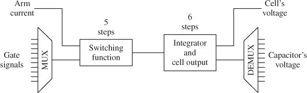
Figure 18B.13 Block diagram of FPGA implementation
Note that the overall process takes 11 time steps, using an internal clock of 10 ns for the FPGA, which means that the first capacitor value will be available after 110 ns. As all of them are time multiplexed by a group of 10, the last capacitor voltage is available after 21 time steps or 210 ns. Here, the advantage of pipelining is very clear, by adding more capacitors in the pipeline, only one more time step is required to obtain the value. In this case, there are still four steps available to add more logic if required, allowing more flexibility as it has been demonstrated in [19].
The implementation from Figure 18B.13 was used to simulate a converter with 500 cells per half-limb, for a total of 3000 cells. It can either use an internal controller, embedded on the FPGA, or an external controller, via optical fiber. In this example, every cell is using two optical fibers for communication: one for receiving data and the other for sending data. Figure 18B.14 shows simulator used to simulate the converter. In the center of the picture is the main simulator where the model is computed with a 250 ns time step. The other racks on each side are only used to manage all the optical fibers that are needed to control the simulation.
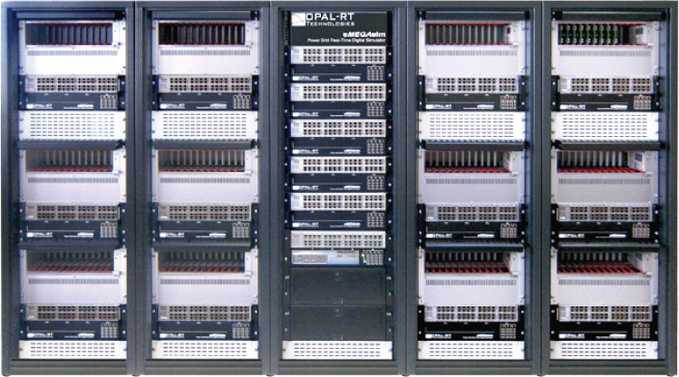
Figure 18B.14 Real-time simulator with I/Os chassis
Figure 18B.15 shows results obtained when changing the power reference. Reactive power is stable at −0.3 pu and the active power changes from 0 to 0.5 pu. Looking at the voltage and current, one can see the phase shift of the current as the active power increases.
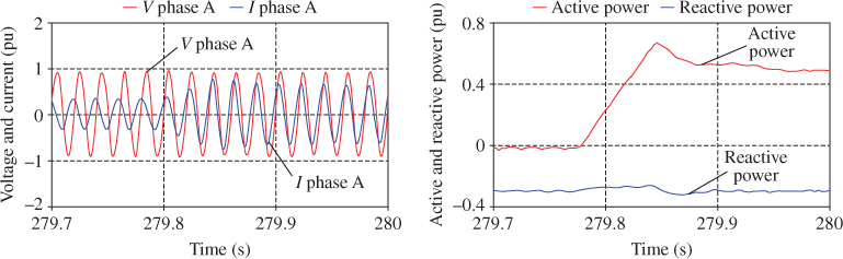
Figure 18B.15 Results of a step on power reference
This is only one of many tests that can be applied to such a system. Using the FPGA implementation allows a very low latency between the I/Os and the model. In this case, only the MMC is simulated on FPGA and the remaining of the network is simulated using processors. In 2011, Nari-Relays Electric Co. in China used the HiL results for the Nanhui MMC demonstration project, 20 MVA/60 kV two-terminal MMC HVDC project.
18B.5 Conclusion
This chapter presented an overview of real-time simulation with a practical application of the different technology. As discussed, the digital simulators are widely used but different technologies are available. Nowadays, understanding the application before acquiring a real-time simulator can help identify the best suited type for the application.
Standard single-processor offline simulation tool does not offers adequate solution to achieve real-time simulation, but it is possible to implement its own design using the different methods proposed in this chapter. Multicore processors, DSP and FPGA, are evolving very fast and therefore so do real-time simulation.
General-purpose electrical solvers are available and being developed to facilitate the use of FPGA technologies by abstracting the inner construction of FPGA chips, as this is done with general-purpose processors. Such FPGA-based solvers should evolve very fast over the next years. This chapter mainly focuses on EMTP simulation, which is the best suited for power electronic simulation, but some softwares are now offering a mix simulation EMTP/phasor; slow components like transmission networks are simulated with phasor algorithm and this simulation is coupled with an EMTP simulation where fast systems, like power electronics, are simulated. Looking to the past 10 years, one can expect that the use of real simulation will keep growing and it seems like it is only limited by the need of the industries.
References
- 1. Lesnicar, A. and Marquardt, R. (2003) An innovative modular multilevel converter topology suitable for a wide power range. 2003 IEEE Power Tech Conference Proceedings, Bologna, Italy, p. 6.
- 2. Hiller, M., Krug, D., Sommer, R., and Rohner, S. (2009) A new highly modular medium voltage converter topology for industrial drive applications. 2009 13th European Conference on Power Electronics and Applications (EPE'09), pp. 1–10.
- 3. Rajasekar, S. and Gupta, R. (2012) Solar photovoltaic power conversion using modular multilevel converter. 2012 Students Conference on Engineering and Systems (SCES), pp. 1–6.
- 4. Peralta, J., Saad, H., Dennetiere, S., and Mahseredjian, J. (2012) Dynamic performance of average-value models for multi-terminal VSC-HVDC systems. 2012 IEEE Power and Energy Society General Meeting, pp. 1–8.
- 5. Zhang, X.Y., Wu, Z.J., Hao, S.P., and Xu, K. (2012) A study on the new grid integration solutions of offshore wind farms. Advanced Materials Research, 383, 3610–3616.
- 6. Callavk, M., Blomberg, A., Häfner, J., and Jacobson, B. (2012) The Hybrid HVDC Breaker an Innovation Breakthrough Enabling Reliable HVDC Grids, http://new.abb.com/docs/default-source/default-document-library/hybrid-hvdc-breaker—an-innovation-breakthrough-for-reliable-hvdc-gridsnov2012finmc20121210_clean.pdf?sfvrsn=2 (accessed 27 December 2013).
- 7. Hartley, T.T., Beale, G.O., and Chicatelli, S.P. (1994) Digital Simulation of Dynamic Systems: A Control Theory Approach, Prentice Hall, Englewood Cliffs, NJ.
- 8. Schaller, R.R. (1997) Moore's law: past, present and future. Spectrum IEEE, 34, 52–59.
- 9. Baracos, P., Murere, G., Rabbath, C., and Jin, W. (2001) Enabling PC-based HIL simulation for automotive applications. 2001 IEEE International Electric Machines and Drives Conference (IEMDC 2001), pp. 721–729.
- 10. Abourida, S., Dufour, C., Bélanger, J. et al. (2002) Real-time PC-based simulator of electric systems and drives. Seventeenth Annual IEEE Applied Power Electronics Conference and Exposition, 2002. APEC 2002, pp. 433–438.
- 11. Dufour, C., Bélanger, J., Ishikawa, T., and Uemura, K. (2005) Advances in real-time simulation of fuel cell hybrid electric vehicles. Proceedings of 21st Electric Vehicle Symposium (EVS-21), Monte Carlo, Monaco.
- 12. Typhoon-HIL http://www.typhoon-hil.com/ (accessed 27 December 2013).
- 13. OPAL-RT Technologies Inc. eFPGAsim Power Electronic Real-Time Simulator. http://www.opal-rt.com/new-product/efpgasim-power-electronic-real-time-simulator(accessed 27 December 2013).
- 14. Hagiwara, M. and Akagi, H. (2009) Control and experiment of pulsewidth-modulated modular multilevel converters. IEEE Transactions on Power Electronics, 24, 1737–1746.
- 15. Antonopoulos, A., Angquist, L., and Nee, H.P. (2009) On dynamics and voltage control of the modular multilevel converter. 13th European Conference on Power Electronics and Applications, 2009. EPE'09, pp. 1–10.
- 16. Zhao, Y., Hu, X.-H., Tang, G.-F., and He, Z.-Y. (2010) A study on MMC model and its current control strategies. 2nd IEEE International Symposium on Power Electronics for Distributed Generation Systems (PEDG), 2010, pp. 259–264.
- 17. Arrillaga, J., Liu, Y.H., and Watson, N.R. (2007) Flexible Power Transmission: The HVDC Options, John Wiley & Sons, Inc..
- 18. Hui, S. and Fung, K. (1997) Fast decoupled simulation of large power electronic systems using new two-port companion link models. IEEE Transactions on Power Electronics, 12, 462–473.
- 19. Gregoire, L.-A., Belanger, J., and Li, W. (2012) FPGA-based real-time simulation of modular multilevel converter HVDC systems. Journal of Energy and Power Engineering, 6, 1119–1125.
- 20. Le-Huy, P., Giroux, P., and Soumagne, J. (2011) Real-time simulation of modular multilevel converters for network integration studies. Proceedings of IPST, p. 6.
- 21. Dufour, C., Mahseredjian, J., and Bélanger, J. (2011) A combined state-space nodal method for the simulation of power system transients. IEEE Transactions on Power Delivery, 26, 928–935.
- 22. Saad, C.D.H., Mahseredjian, J., Dennetière, S., and Nguefeu, S. (2013) Real time simulation of MMCs using the state-space nodal approach. Presented at the International Conference on Power Systems Transients, Vancouver, Canada.
- 23. Zeigler, B.P., Praehofer, H., and Kim, T.G. (2000) Theory of Modeling and Simulation: Integrating Discrete Event and Continuous Complex Dynamic Systems, Academic Press, San Diego, CA.
- 24. Hudson, J.E., Hunter, E.M., and Wilson, D.D. (1966) EHV-DC simulator. IEEE Transactions on Power Apparatus and Systems, PAS-85, 1101–1107.
- 25. OPAL-RT Technologies Inc. HYPERSIM Power System Real-Time Simulator, http://www.opal-rt.com/new-product/hypersim-power-system-real-time-simulator (accessed 27 December 2013).
- 26. Gagnon, R., Fecteau, M., Prud'Homme, P. et al. (2012) Hydro-Québec strategy to evaluate electrical transients following wind power plant integration in the Gaspésie transmission system. IEEE Transactions on Sustainable Energy, 3, 880.
- 27. OPAL-RT Technologies Inc. ePOWERgrid Product Family Overview, http://www.opal-rt.com/epowergrid-product-family-overview (accessed 27 December 2013).
- 28. RTDS Technologies High Speed Power System Studies, http://www.rtds.com/applications/high-speed-power-system-studies/high-speed-power-system-studies.html (accessed 27 December 2013).
- 29. Dufour, C., Cense, S., Ould-Bachir, T. et al. (2012) General-purpose reconfigurable low-latency electric circuit and motor drive solver on FPGA. IECON 2012-38th Annual Conference on IEEE Industrial Electronics Society, pp. 3073–3081.
- 30. Paquin, J.-N., Bélanger, J., Snider, L.A. et al. (2009) Monte-carlo study on a large-scale power system model in real-time using emegasim. 2009 IEEE Energy Conversion Congress and Exposition (ECCE 2009), San Jose, CA, pp. 3194–3202.