Universidad de Concepción
Pontificia Universidad Católica de Chile
Universidad de Concepción
Universidad Téchnica Federico Santa María
Shunt Compensation Principles • Traditional Shunt Compensation • Self-Commutated Shunt Compensators • Comparison between Thyristorized and Self-Commutated Compensators • Superconducting Magnetic Energy Storage
Series Compensation Principles • Static Synchronous Series Compensator • Thyristor-Controlled Series Compensation
Unified Power Flow Controller • Interline Power Flow Controller • Unified Power Quality Conditioner
27.5 Facts Controller’s Applications
500 kV Winnipeg-Minnesota Interconnection (Canada-USA) • Channel Tunnel Rail Link • STATCOM “Voltage Controller” ±100 MVAr STATCOM at Sullivan Substation (TVA) in Northeastern Tennessee • Unified Power Flow Controller “All Transmission Parameters Controller”: ±160 MVA Shunt and ±160 MVA Series at Inez Substation (AEP), Northeastern Virginia, USA • Convertible Static Compensator in the New York 345 kV Transmission System
In the last decades power systems have faced new challenges due to deregulation, permanent increase in demand, the implementation of more stringent standard, and lack of investment in new transmission lines. The privatization of utilities has created a new electric power market scenario and a more complicated power system operation. Also, the increased dependence of modern society upon electricity has forced power systems to operate with very high reliability and with almost 100% availability. Moreover, power quality is now becoming a major concern among users and utilities, forcing the development and application of more stringent standards due to the connection of more sophisticated loads. These requirements have obliged to develop new technologies to improve power system operation and controllability. Based in these new technologies two concepts have been created: flexible ac transmission systems (FACTS) and flexible reliable and intelligent electrical energy delivery systems (FRIENDS). In these systems, compensation equipments based in static converters play an important role [1,2].
The FACTS concept was originally created in the 1980s to solve operation problems due to the restrictions on the construction of new transmission lines, to improve power system stability margins, and to facilitate power exchange between different generation companies and large power users. On the other hand, the FRIENDS concept was created in the 1990s and identifies the operation of utilities with new static compensators and communication systems whose goal is to develop a desirable structure for power delivery systems where distributed generations and distributed energy storage systems are located near the load side. Finally, custom power devices are special applications of FACTS, but oriented to satisfy requirements of power quality at the utility level [5].
The two main objectives of FACTS are to increase the power transfer capability of transmission lines and to maintain the power flow over designated routes. The first objective implies that power flow in a given line should be able to be increased up to the thermal limit by forcing the rated current through the series line impedance. This objective does not mean that the lines would normally be operated at their thermal limit (the transmission losses would be unacceptable), but this option would be available, if needed, to handle severe system contingencies. The second objective implies that, by being able to control the current in a line (for example by changing the effective line impedance) the power flow can be restricted to selected transmission corridors. The achievement of these two basic objectives significantly increases the utilization of existing (and new) transmission assets, and plays a major role in facilitating deregulation [9].
Therefore, the FACTS technology opens up new opportunities for controlling power and enhancing the usable capacity of present transmission systems. The possibility that power through a line can be controlled enables a large potential of increasing the capacity of existing lines. These opportunities arise through the ability of FACTS controllers to adjust the power system electrical parameters including series and shunt impedances, current, voltage, phase angle, and the damping oscillations. The implementation of such equipments requires the development of power electronics-based compensators and controllers. The coordination and overall control of these compensators to provide maximum system benefits and prevent undesirable interactions with different system configurations under normal and contingency conditions present a different technological challenge. This challenge is the development of appropriate system optimization control strategies, communication links, and security protocols.
The IEEE Power Engineering Society (PES) Task Force of the FACTS Working Group defined terms and definitions for FACTS and FACTS controllers. According with this IEEE Working Group, a FACTS controller is a power electronic-based system and other static equipment that provide control of one or more ac transmission system parameters [3].
Different types of FACTS controllers have been developed and implemented, for shunt and/or series compensation. Shunt compensation is used to influence the natural electrical characteristics of the transmission line to increase steady-state transmittable power and to control voltage profile along the line, while series compensation is used to change the transmission line impedance and is highly effective in controlling power flow through the line and in improving system stability. Most of FACTS controllers act over the reactive power flow in order to control voltage profile and to increase power system stability. The concept of VAR compensation using FACTS controllers embraces a wide and diverse field of both transmission system and customer problems, especially related with power quality issues, since most of power quality problems can be attenuated or solved with an adequate control of reactive power [4]. In general, the problem of reactive power compensation is viewed from two aspects: load compensation and voltage support. In load compensation the objectives are to increase the value of the system power factor, to balance the real power drawn from the ac supply, compensate voltage regulation, and to eliminate current harmonic components produced by large and fluctuating nonlinear industrial loads [6]. Voltage support is generally required to reduce voltage fluctuation at a given terminal of a transmission line. Reactive power compensation in transmission systems also improves the stability of the ac system by increasing the maximum active power that can be transmitted. It also helps to maintain a substantially flat voltage profile at all levels of power transmission, it improves HVDC conversion terminal performance, increases transmission efficiency, controls steady-state and temporary overvoltages, and can avoid disastrous blackouts [7,8].
Based on the use of reliable high-speed power electronics, powerful analytical tools, advanced control and microcomputer technologies, static compensators also known as FACTS controllers have been developed and represent a new concept for the operation of power transmission systems. This chapter presents the principles of operation and performance characteristics of different FACTS controllers. Static compensators implemented with thyristors and self-commutated converters are described. New static compensators such as static synchronous compensators (STATCOMs), unified power flow controllers (UPFC), dynamic voltage restorers (DVR), required to compensate modern power transmission and distribution systems are also presented and described [10].
Shunt compensation is used basically to control the amount of reactive power that flows through the power system. In a linear circuit, the reactive power is defined as the ac component of the instantaneous power, with a frequency equal to 100/120 Hz in a 50 or 60 Hz system. The reactive power generated by the ac power source is stored in a capacitor or a reactor during a quarter of a cycle, and in the next quarter cycle is sent back to the power source. The reactive power oscillates between the ac source and the capacitor or reactor, and also between them, at a frequency equal to two times the rated value (50 or 60 Hz). For this reason it can be compensated using static equipments or VAR generators, avoiding its circulation between the load (inductive or capacitive) and the source, and therefore improving voltage regulation and stability of the power system. Reactive power compensation can be implemented with VAR generators connected in parallel or in series [11].
27.2.1 Shunt Compensation Principles
Figure 27.1 shows the principles and theoretical effects of shunt reactive power compensation in a basic ac system, which comprises a source V1, a transmission line, and a typical inductive load. Figure 27.1a shows the system without compensation, and its associated phasor diagram. In the phasor diagram, the phase angle of the current has been related to the load side, which means that the active current IP is in phase with the load voltage V2. Since the load is assumed inductive, it requires reactive power for proper operation, which must be supplied by the source, increasing the current flow from the generator and through the lines. If reactive power is supplied near the load, the line current is minimized, reducing power losses and improving voltage regulation at the load terminals. This can be done with a capacitor, with a voltage source, or with a current source. In Figure 27.1b, a current-source device is being used to compensate the reactive component of the load current (IQ). As a result, the system voltage regulation is improved and the reactive current component from the source is almost eliminated.
A current source or a voltage source can be used for reactive shunt compensation. The main advantages of using voltage- or current-source VAR generators (instead of inductors or capacitors) are that the reactive power generated is independent of the voltage at the point of connection and can be adjusted in a wide range.
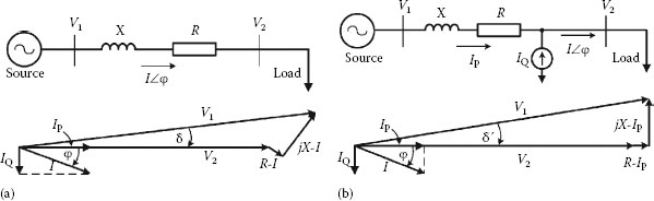
FIGURE 27.1 Principles of shunt compensation in a radial ac system. (a) System phasor diagram without reactive compensation. (b) Shunt compensation of the system with a current source.
Since shunt compensation is able to change the power flow in the system by varying the value of the applied shunt equivalent impedance, changing the reactive power flow in the system, during and following dynamic disturbances, the transient stability limit can be increased and effective power oscillation damping can be provided. Thereby, the voltage of the transmission line counteracts the accelerating swings of the disturbed machine and therefore damps the power oscillations.
Independent of the source type or system configuration, different requirements have to be taken into consideration for a successful operation of shunt compensators. Some of these requirements are simplicity, controllability, time response, cost, reliability, and harmonic distortion.
27.2.2 Traditional Shunt Compensation
In general, shunt compensators are classified depending on the technology used in their implementation. Rotating and static equipments were commonly used to compensate reactive power and to stabilize power systems. In the last decades, a large number of different static FACTS controllers, using power electronic technologies and digital control schemes have been proposed and developed [11]. There are two approaches to the realization of power electronics-based compensators: the one that employs thyristor-switched capacitors and reactors with tap-changing transformers, and the other group that uses self-commutated static converters. A brief description of the most commonly used shunt compensators is presented below.
27.2.2.1 Fixed or Mechanically Switched Capacitors
Shunt capacitors were first employed for power factor correction in the year 1914 [12]. The leading current drawn by the shunt capacitors compensates the lagging current drawn by the load. The selection of shunt capacitors depends on many factors, the most important of which is the amount of lagging reactive power taken by the load. In the case of widely fluctuating loads, the reactive power also varies over a wide range. Thus, a fixed capacitor bank may often lead to either over-compensation or under-compensation. Variable VAR compensation is achieved using switched capacitors [13]. Depending on the total VAR requirement, capacitor banks are switched into or switched out of the system. The smoothness of control is solely dependent on the number of capacitors switching units used. The switching is usually accomplished using relays and circuit breakers. However, these methods based on mechanical switches and relays have the disadvantage of being sluggish and unreliable. Also, they generate high inrush currents, and require frequent maintenance.
27.2.2.2 Synchronous Condensers
Synchronous condensers have played a major role in voltage and reactive power control for more than 50 years. Functionally, a synchronous condenser is simply a synchronous machine connected to the power system. After the unit is synchronized, the field current is adjusted to either generate or absorb reactive power as required by the ac system. The machine can provide continuous reactive power control when used with the proper automatic exciter circuit. Synchronous condensers have been used at both distribution and transmission voltage levels to improve stability and to maintain voltages within desired limits under varying load conditions and contingency situations. However, synchronous condensers are rarely used today because they require substantial foundations and a significant amount of starting and protective equipment. They also contribute to the short circuit current and they cannot be controlled fast enough to compensate rapid load changes. Moreover, their losses are much higher than those associated with static compensators, and the cost is much higher as well. Their advantage lies in their high temporary overload capability [4].
27.2.2.3 thyristorized VAR Compensators
As in the case of the synchronous condenser, the aim of achieving fine control over the entire VAR range, has been fulfilled with the development of static compensators but with the advantage of faster response times [11]. Thyristorized VAR compensators consist of standard reactive power shunt elements (reactors and capacitors) which are controlled to provide rapid and variable reactive power. They can be grouped into two basic categories, the thyristor-switched capacitor (TSC) and the thyristor-controlled reactor (TCR).
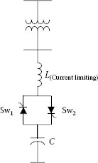
FIGURE 27.2 The thyristor-switched capacitor configuration.
27.2.2.3.1 Thyristor-Switched Capacitors
Figure 27.2 shows the basic scheme of a static compensator of the TSC type. First introduced by ASEA in 1971 [12], the shunt capacitor bank is split up into appropriately small steps, which are individually switched in and out using bidirectional thyristor switches. Each single-phase branch consists of two major parts, the capacitor C and the thyristor switches Sw1 and Sw2. In addition, there is a minor component, the inductor L, whose purpose is to limit the rate of rise of the current through the thyristors and to prevent resonance with the network (normally 6% with respect to XC). The capacitor may be switched with a minimum of transients if the thyristor is turned on at the instant when the capacitor voltage and the network voltage have the same value. Static compensators of the TSC type have the following properties: stepwise control, average delay of one half a cycle (maximum one cycle), and no generation of harmonics since current transient component can be attenuated effectively [12,13].
The current that flows through the capacitor at a given time t is defined by the following expression:
(27.1) |
where
XC and XL are the compensator capacitive and inductive reactances
Vm the source maximum instantaneous voltage
α the voltage phase-shift angle at which the capacitor is connected
ωr the system resonant frequency
VC0 is the capacitor voltage at t = 0−
Expression (27.1) has been obtained assuming that the system equivalent resistance is negligible as compared with the system reactance. This assumption is valid in high-voltage transmission lines. If the capacitor is connected at the moment that the source voltage is maximum and VC0 is equal to the source voltage peak value, Vm (α = ±90°) the current transient component is zero.
Despite the attractive theoretical simplicity of the switched capacitor scheme, its popularity has been hindered by a number of practical disadvantages: the VAR compensation is not continuous, each capacitor bank requires a separate thyristor switch and therefore the construction is not economical, the steady-state voltage across the nonconducting thyristor switch is twice the peak supply voltage, and the thyristor must be rated for or protected by external means against line voltage transients and fault currents.
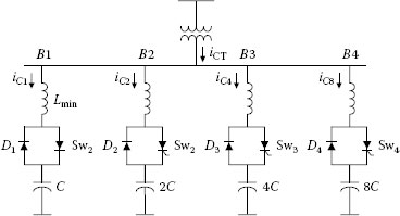
FIGURE 27.3 Binary rated thyristor-diode-switched capacitor configuration.
An attractive solution to the disadvantages of using TSC is to replace one of the thyristor switches by a diode. In this case, inrush currents are eliminated when thyristors are fired at the right time, and a more continuous reactive power control can be achieved if the rated power of each capacitor bank is selected following a binary combination, as described in Ref. [14]. This configuration is shown in Figure 27.3. In this figure, the inductor Lmin is used to prevent any inrush current produced by a firing pulse out of time.
To connect each branch, a firing pulse is applied at the thyristor gate, but only when the voltage supply reaches its maximum negative value. In this way, a soft connection is obtained [1]. The current will increase starting from zero without distortion, following a sinusoidal waveform, and after the cycle is completed, the capacitor voltage will have the voltage −Vm, and the thyristor automatically will block. In this form of operation, both connection and disconnection of the branch will be soft, and without transient component. If the firing pulses and the voltage −Vm are properly adjusted, neither harmonics nor inrush currents are generated, since two important conditions are achieved: dv/dt at v = −Vm is zero, and anode-to-cathode thyristor voltage is equal to zero. Assuming that v(t) = Vm sin ωt is the source voltage, VC;0 the initial capacitor voltage, and vTh(t) the thyristor anode-to-cathode voltage, the right connection of the branch will be when vTh(t) = 0, that is
(27.2) |
since VC0 = −Vm:
(27.3) |
then, vTh(t) = 0 when sin ωt = −1 ⇒ ωt = 270°.
At ωt = 270°, the thyristor is switched on, and the capacitor C begins to discharge. At this point, sin(270°) = -cos(0°), and hence vC(t) for ωt ≥ 270° will be: VC (t0) = −Vm cos ωt0. The compensating capacitor current starting at t0 will be
(27.4) |
Equation 27.4 shows that the current starts from zero as a sinusoidal waveform without distortion and/or inrush component. If the above switching conditions are satisfied, the inductor L may be minimized or even eliminated.
The experimental oscillograms of Figure 27.4 show how the binary connection of many branches allows an almost continuous compensating current variation. These experimental current waveforms were obtained in a 5 kVAr laboratory prototype. The advantages of this topology are that many compensation levels can be implemented with few branches allowing continuous variations without distortion. Moreover, the topology is simpler and more economical as compared with TSC. The main drawback is that it has a time delay of one complete cycle compared with the half cycle of TSC.

FIGURE 27.4 Experimental compensating phase current of the thyristor-diode switched capacitor: (a) current through B1; (b) current through B2; (c) current through B3; (d) current through B4, and (e) total system compensating current.
27.2.2.3.2 Thyristor-Controlled Reactor
Figure 27.5 shows the power scheme of a static compensator of the TCR type. In most cases, the compensator also includes a fixed capacitor or a filter for low order harmonics, which is not shown in this figure. Each of the three phase branches includes an inductor L, and the thyristor switches Sw1 and Sw2. Reactors may be both switched and phase-angle controlled [15–17].
When phase-angle control is used, a continuous range of reactive power consumption is obtained. It results, however, in the generation of odd harmonic current components during the control process. Full conduction is achieved with a gating angle of 90°. Partial conduction is obtained with gating angles between 90° and 180°, as shown in Figure 27.6. By increasing the thyristor gating angle, the fundamental component of the current reactor is reduced. This is equivalent to increase the inductance, reducing the reactive power absorbed by the static compensator.
However, it should be pointed out that the change in the reactor current may only take place at discrete points of time, which means that adjustments cannot be made quicker than once per half cycle. Static compensators of the TCR type are characterized by the ability to perform continuous control, with maximum delay of one-half cycle and practically no transients. The principal disadvantages of this configuration are the generation of low frequency harmonic current components, and higher losses when working in the inductive region (i.e., absorbing reactive power). The relation between the fundamental component of the reactor current and the phase-shift angle α is given by

FIGURE 27.5 The thyristor-controlled reactor configuration.
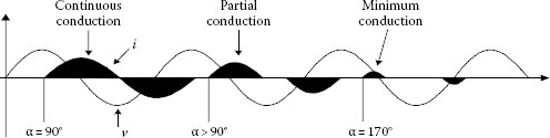
FIGURE 27.6 Simulated voltage and current waveforms in a TCR for different thyristor phase-shift angles, α.
(27.5) |
In a single-phase unit, with balanced phase-shift angles, only odd harmonic components are presented in the reactor current. The amplitude of each harmonic component is defined by
(27.6) |
In order to eliminate low frequency current harmonics (third, fifth, seventh), delta configurations (for zero sequence harmonics) and passive filters may be used, as shown in Figure 27.7a. Twelve pulse configurations are also used as shown in Figure 27.7b. In this case, passive filters are not required, since the fifth and seventh current harmonics are eliminated by the phase-shift introduced by the transformer.
27.2.2.3.3 VAR Compensation Characteristics
One of the main characteristics of static VAR compensators is that the amount of reactive power interchanged with the system depends on the applied voltage, as shown in Figure 27.8. This figure displays the steady-state VT – Q characteristics of a combination of fixed capacitor–thyristor-controlled reactor (FC–TCR) compensator. This characteristic shows the amount of reactive power generated or absorbed by the FC–TCR, as a function of the applied voltage. At rated voltage, the FC–TCR presents a linear characteristic, which is limited by the rated power of the capacitor and reactor respectively. Beyond these limits, the VT – Q characteristic is not linear, which is one of the main disadvantages of this type of VAR compensator.
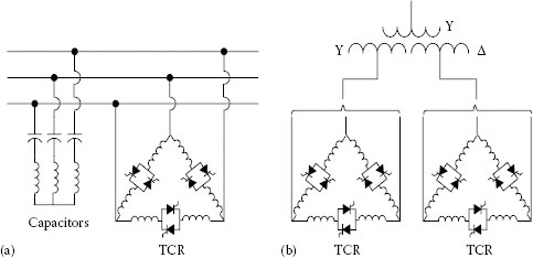
FIGURE 27.7 Fixed capacitor-thyristor-controlled reactor configuration. (a) Six pulse topology. (b) Twelve-pulse topology.

FIGURE 27.8 Voltage–reactive power characteristic of a FC–TCR.
27.2.2.3.4 Combined Thyristor-Switched Capacitor and Thyristor-Controlled Reactor
Irrespective of the reactive power control range required, any static compensator can be built up from one or both of the above-mentioned schemes (i.e., TSC and TCR), as shown in Figure 27.9. In those cases where the system with switched capacitors is used, the reactive power is divided into a suitable number of steps and the variation will therefore take place stepwise. Continuous control may be obtained with the addition of a TCR. If it is required to absorb reactive power, the entire capacitor bank is disconnected and the equalizing reactor becomes responsible for the absorption. By coordinating the control between the reactor and the capacitor steps, it is possible to obtain fully stepless control. Static compensators of the combined TSC and TCR type are characterized by a continuous control, practically no transients, low generation of harmonics (because the controlled reactor rating is small compared to the total reactive power), and flexibility in control and operation. An obvious disadvantage of the TSC–TCR as compared with TCR- and TSC-type compensators is the higher cost. A smaller TCR rating results in some savings, but these savings are more than absorbed by the cost of the capacitor switches and the more complex control system [12].
The voltage–current characteristic of this compensator is shown in Figure 27.10.
To reduce transient phenomena and harmonic distortion, and to improve the dynamics of the compensator, some researchers have applied self-commutation to TSC and TCR. Some examples of this can be found in Refs. [18,19]. However, best results have been obtained using self-commutated compensators based on conventional two-level and three-level inverters [20].
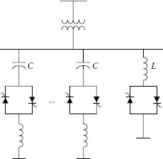
FIGURE 27.9 Combined TSC and TCR configuration.

FIGURE 27.10 Steady-state voltage-current characteristic of a combined TSC–TCR compensator.
27.2.3 Self-Commutated Shunt Compensators
The application of self-commutated converters as a means of compensating reactive power has demonstrated to be an effective solution. This technology has been used to implement more sophisticated compensator equipment such as STATCOM, UPFC, and dynamic voltage compensators [3,21]. The STATCOM is based on a solid-state voltage source, implemented with an inverter, and connected in parallel to the power system through a coupling reactor, in analogy with a synchronous machine, generating balanced set of three sinusoidal voltages at the fundamental frequency, with controllable amplitude and phase-shift angle. A STATCOM is a controlled reactive power source. This equipment, however, has no inertia and limited overload capability. Examples of these topologies are shown in Figures 27.11 and 27.12 [10,21].

FIGURE 27.11 A VAR compensator topology implemented with a current-source converter.

FIGURE 27.12 A VAR compensator topology implemented with a voltage-source converter.
27.2.3.1 Principles of Operation
With the remarkable progress of gate commutated semiconductor devices, attention has been focused on self-commutated FACTS controllers capable of generating or absorbing reactive power without requiring large banks of capacitors or reactors. Several approaches are possible including current-source and voltage-source converters. The current-source approach shown in Figure 27.11 uses a reactor supplied with a regulated dc current, while the voltage-source inverter, displayed in Figure 27.12, uses a capacitor with a regulated dc voltage.
The principal advantages of self-commutated FACTS controllers are the significant reduction of size and the potential reduction in cost achieved from the elimination of a large number of passive components and lower relative capacity requirement for the semiconductor switches [20,21]. Because of its smaller size, self-commutated VAR compensators are well suited for applications where space is a premium.
Self-commutated compensators are used to stabilize transmission systems, improve voltage regulation, correct power factor, and also correct load unbalances [22]. Moreover, they can be used for the implementation of shunt and series compensators. Figure 27.13 shows a shunt STATCOM, implemented with a boost type voltage-source converter. Neglecting the internal power losses of the overall converter, the control of the reactive power is done by adjusting the amplitude of the fundamental component of the output voltage VMOD, which can be modified with the PWM pattern as shown in Figure 27.14. When VMOD is larger than the voltage VCOMP, the VAR compensator generates reactive power (Figure 27.13b) and when VMOD is smaller than VCOMP, the compensator absorbs reactive power (Figure 27.13c). Its principle of operation is similar to the synchronous machine. The compensation current can be leading or lagging, depending on the relative amplitudes of VCOMP and VMOD. The capacitor voltage VD, connected to the dc link of the converter, is kept equal to a reference value VREF through of a special feedback control loop, which controls the phase-shift angle, δ, between VCOMP and VMOD.
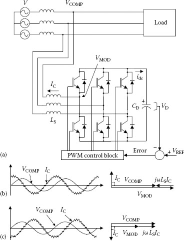
FIGURE 27.13 Simulated current and voltage waveforms of a voltage-source self-commutated shunt VAR compensator. (a) STATCOM topology. (b) Simulated current and voltage waveforms for leading compensation (VMOD > VCOMP). (c) Simulated current and voltage waveforms for lagging compensation (VMOD < VCOMP).
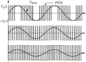
FIGURE 27.14 Simulated compensator output voltage waveform for different modulation index (amplitude of the fundamental voltage component).
The amplitude of the compensator output voltage (VMOD) can be controlled by changing the switching pattern modulation index (Figure 27.14), or by changing the amplitude of the converter dc voltage VD. Faster time response is achieved by changing the switching pattern modulation index instead of VD. The converter dc voltage VD, is changed by adjusting the small amount of active power absorbed by the converter and defined by
(27.7) |
where
XS is the converter link reactor
δ is the phase-shift angle between voltages VCOMP and VMOD
To increase the amplitude of VD a small positive average value of current must circulate through the dc capacitor so that VD will increase until it reaches the required value. In the same way, if it is necessary to decrease the amplitude of VD then a small negative average value of current must flow through the dc capacitor. The active power flow of the converter is defined by δ. If δ is positive the converter absorbs active power (increasing VD), and if δ is negative the converter generates active power, and therefore VD decreases.
One of the major problems that must be solved when self-commutated converters are used in high-voltage systems is the limited capacity of the gate-controlled semiconductors available in the market (IGBTs and IGCTs). Actual semiconductors can handle a few thousands of amperes and 6–10 kV reverse voltage blocking capabilities, which is clearly not enough for high-voltage applications. This problem can be overcome by using more sophisticated converters topologies, as described below.
27.2.3.2 Multilevel Converters
Multilevel converters are being investigated and some topologies are used today as STATCOM. The main advantages of multilevel converters are less harmonic generation and higher voltage capability because of serial connection of bridges or semiconductors. The most popular arrangement today is the three-level neutral-point clamped (NPC) topology.
27.2.3.2.1 Three-Level Neutral-Point Clamped Topology
Figure 27.15 shows a STATCOM implemented with a three-level NPC converter. Three-level converters [23] are becoming the standard topology for medium voltage converter applications, such as machine drives and active front-end rectifiers. The advantage of three-level converters is that they can reduce the generated harmonic content, for the same switching frequency, since they produce a voltage waveform with more levels than the conventional two-level topology. Another advantage is that they can reduce the semiconductor voltage rating and the associated switching frequency. Three-level converters consist of 12 self-commutated semiconductors such as IGBTs or IGCTs, each of them shunted by a reverse parallel connected power diode, and 6 diode branches connected between the midpoint of the dc link bus and the midpoint of each pair of switches as shown in Figure 27.15. By connecting the dc source sequentially to the output terminals, the converter can produce a set of PWM signals in which the frequency, amplitude, and phase of the ac voltage can be modified with adequate control signals.
27.2.3.2.2 Multilevel Converters with Single-Phase Inverters
Another exciting technology that has been successfully proven uses basic “H” bridges as shown in Figure 27.16, connected to line through power transformers. The system uses sinusoidal pulse width modulation (SPWM) with triangular carriers shifted and depending on the number of converters connected in the chain of bridges, the voltage waveform becomes more and more sinusoidal. Figure 27.16a shows one phase of this topology implemented with eight “H” bridges and Figure 27.16b shows the voltage waveforms obtained as a function of number of “H” bridges.
An interesting result with this converter is that the ac voltages become modulated by pulse width and by amplitude (PWM and AM). This is because when the pulse modulation changes, the steps of the amplitude also change. The maximum number of steps of the resultant voltage is equal to two times the number of converters plus the zero level. Then, four bridges will result in a nine-level converter per phase.

FIGURE 27.15 A STATCOM implemented with a three-level NPC inverter.
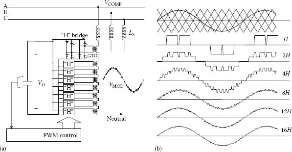
FIGURE 27.16 Multilevel STATCOM implemented with “H” bridge converters and associated voltage waveforms. (a) Multilevel converter with eight “H” bridges per phase and triangular carriers shifted. (b) Voltage waveforms as a function of number of bridges.
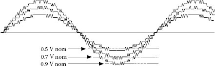
FIGURE 27.17 Amplitude modulation in the voltage waveform topology of Figure 27.16.
Figure 27.17 shows the principles of AM operation. When the voltage decreases, some steps disappear, and then the amplitude modulation becomes a discrete function.
27.2.3.2.3 Optimized Multilevel Converter
The number of levels can increase rapidly with few converters when voltage escalation is applied. In a similar way of converter in Figure 27.16, the topology of Figure 27.18 has a common dc link with voltage isolation through output transformers, connected in series at the line side. However, the voltages at the line side are scaled in power of three. By using this strategy, the number of voltage steps is maximized and few converters are required to obtain almost sinusoidal voltage waveforms. In the topology of Figure 27.18, amplitude modulation with 81 levels of voltage is obtained using only 4 “H” converters per phase (4-stage inverter). In this way, STATCOMs with “harmonic-free” characteristics can be implemented.
It is important to remark that the bridge with the higher voltage is being commutated at the line frequency, which is a major advantage of this topology for high power applications. Another interesting characteristic of this converter, compared with the multilevel strategy with carriers shifted, is that only 4 “H” bridges per phase are required to get 81 levels of voltage. In the previous multilevel converter with carriers shifted, 40 “H” bridges instead of four are required. For high power applications, probably a less complicated three-stage (3 “H” bridges per phase) is enough. In this case, 27 levels or steps of voltage are obtained, which will provide good enough voltage and current waveforms for high-quality operation [26].
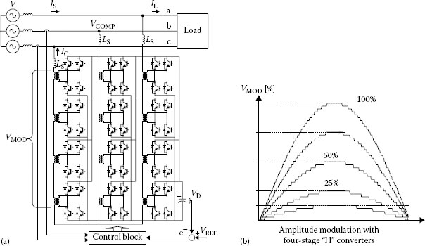
FIGURE 27.18 Optimized STATCOM using “H” bridges converters. (a) Four-stage, 81-level STATCOM, using “H” bridges scaled in power of three; (b) converter output voltage using amplitude modulation.
27.2.3.3 STATCOM Design Principles
The principal components of the STATCOM are the PWM converter, the coupling reactor, and the dc capacitor. The converter topology depends on the rated voltage and power, and can be implemented with a voltage- or current-source approach, although most of the STATCOM have been implemented using voltage-source converters. The design of the coupling reactor and dc capacitor is based on the functions they perform. The main purpose of the coupling reactor is to absorb the instantaneous voltage difference that appears between the utility voltage and the converter input voltage. Also, in case of using a voltage-source converter, the reactor helps to reduce the harmonic distortion of the line current, and can contribute to stabilize the converter switching frequency.
27.2.3.3.1 Coupling Reactor Design
Two criteria have been used to design the coupling reactor. The first one is based in the maximum current harmonic allowed in the input current and the second one is related with the control scheme implemented in the current loop. In the first case, the reactor value is given by expression
(27.8) |
where
THDi is the maximum harmonic distortion allowed in the converter input current (normally 5%)
Vak the converter input voltage harmonic component
k the order of the harmonic component
The converter input voltage, Vak, depends on the PWM technique implemented in the converter.
In case a current control loop is implemented, the reactor value must be rated in order to allow intersections between the current reference and the converter input current. The block diagram of a typical current control scheme used in STATCOM is shown in Figure 27.19. The principal advantage of this current control scheme is that it forces the converter to operate with constant switching frequency. The constant switching frequency is achieved by comparing the current error signal with a triangular reference waveform. The purpose of introducing the triangular waveform is to stabilize the inverter switching frequency by forcing it to be constant and equal to the frequency of the triangular reference.
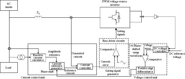
FIGURE 27.19 The block diagram of a current controlled STATCOM.
The current control method can be explained by considering the hysteresis technique plus the addition of a fixed frequency triangular waveform inside the imaginary hysteresis window (Figure 27.20). If the current reference, is⋆, is higher than the generated current, is, the error waveform is positive and when compared with the triangular waveform it results in a positive pulse. This pulse will then turn on an inverter bottom switch that will increase the corresponding output line current. In the same way, if is⋆ is lower than is, the error waveform is negative and the gating signals are adjusted so that the line current decreases (a top switch is turned on). The slope of the error signal is chosen to be always smaller than the slope of the triangular waveform in order to ensure that an intersection between the two signals exists. Thus, the current error signal is forced to remain between the maximum and the minimum of the triangular waveform and as a result, the line current follows the reference closely. Moreover, since the error between is⋆ and is is always kept within the positive and negative peaks of the triangular waveform, the system has an inherent overcurrent protection. However, a large variation in the reference current will generate a large error signal, which can be higher than the amplitude of the triangular waveform. In this case there will not be an intersection between the error and the triangular waveform, thus the switching pattern will not change until the error is reduced and a new intersection occurs.

FIGURE 27.20 Principles of operation of the fixed switching frequency current control technique.
The minimum amplitude of the triangular waveform is determined by the maximum slope of the error, which is in turn fixed by the maximum slope of the line current. The maximum slope of the line current is determined by the maximum instantaneous voltage drop across the coupling reactor and the value of the inductance. Reducing the amplitude of the triangular waveform below this value will generate multiple crossing between the current error and the triangular signals thus disturbing the operation of the inverter. The value of the coupling reactor inductance is obtained from expression
(27.9) |
where
ΔVreactor is the maximum expected voltage drop across the coupling reactor
Atriangular the amplitude of the triangular control waveform
ft the triangular waveform frequency (equals to the converter switching frequency)
27.2.3.3.2 dc Capacitor Design
The function of the dc capacitor is to maintain a dc voltage constant and equal to the reference value imposed by the control scheme. In theory, the dc capacitor is not used as an energy storage element, although it may be necessary to compensate active power in case of outage, especially in industrial applications. Two design criteria are used to calculate the capacitance value. The first is related with the maximum voltage harmonic distortion factor allowed in the dc voltage, and the second one with the maximum voltage fluctuation that can be tolerated in the dc voltage in case of load rejection or a step increase in the load power. In the first case the capacitance is obtained with expression (27.9), and in the second one (maximum voltage fluctuation) with expression (27.10). If the dc capacitor is designed with the constraint that with rated leading var compensation, the ripple factor for VD is less than a given value, the capacitance is defined by expression
(27.10) |
where
RV is the maximum voltage ripple factor across the dc capacitor
Ick the capacitor current harmonic component
Independently of the STATCOM control scheme, an overvoltage is created when the converter line currents are forced to reduce their amplitude, or when they are forced to change from a 90° leading to a 90° lagging phase-shift. On the other hand, an undervoltage is generated when the line currents are forced to increase their amplitude, or when they are forced to change from a 90° lagging to a 90° leading phase-shift. These dc voltage fluctuations are created because transiently the dc capacitor supplies (or absorbs) the extra power required by the system. The amplitude of this voltage fluctuation depends on the instant at which the transient occurs and on the amount of change in the line current amplitude. The maximum overvoltage is generated when one of the line currents is forced to change from 1 per unit leading to 1 per unit lagging, and can be calculated using expression
(27.11) |
where
VD max is the maximum overvoltage across the dc capacitor
VD0 is the steady-state dc voltage
ic is the instantaneous capacitor current
The dc current ic(t) is defined by the product of the converter line currents with the respective switching functions. The principal design constraint for C is to keep the voltage fluctuation below a defined value, ΔV, that is
(27.12) |
Comparing the two design criteria, the second one provides a larger value of C, which contributes to increase the STATCOM stability, making its operation safer.
27.2.3.4 Semiconductor Devices Used for Self-Commutated STATCOMs and FACTS Controllers
Three are the most relevant devices for applications in self-commutated STATCOMs or other FACTS controllers: thyristors, insulated gate bipolar transistors (IGBTs), and integrated gate controlled thyristors (IGCTs). This field of application requires that the semiconductor must be able to block high voltages in the kV range. High-voltage IGBTs required to apply self-commutated converters in FACTS controllers reach now the level of 6.5 kV, allowing for the construction of circuits with a power of several MVA. Also IGCTs are reaching levels higher than 6 kV. Perhaps, the most important development in semiconductors for high-voltage applications is the light triggered thyristor (LTT). This device is the most important for ultrahigh power applications. Recently, LTT devices have been developed with a capability of up to 13.5 kV and a current of up to 6 kA. These new devices reduce the number of elements in series and in parallel, reducing consequently the number of gate and protection circuits. With these elements, it is possible to reduce cost and increase rated power in FACTS installations of up to several hundreds of MVARs [24].
27.2.4 Comparison between thyristorized and Self-Commutated Compensators
Thyristorized and self-commutated FACTS controllers are very similar in their functional compensation capability, but the basic operating principles, as shown, are fundamentally different. A STATCOM functions as a shunt-connected synchronous voltage source whereas a thyristorized compensator operates as a shunt-connected, controlled reactive admittance. This difference accounts for the STATCOM’s superior functional characteristics, better performance, and greater application flexibility.
In the linear operating range of the V–I characteristic, the functional compensation capability of the STATCOM and Static VAR Compensator (SVC) is similar. Concerning the nonlinear operating range, the STATCOM is able to control its output current over the rated maximum capacitive or inductive range independently of the ac system voltage, whereas the maximum attainable compensating current of the SVC decreases linearly with ac voltage. Thus, the STATCOM is more effective than the SVC in providing voltage support under large system disturbances during which the voltage excursions would be well outside of the linear operating range of the compensator. The ability of the STATCOM to maintain full capacitive output current at low system voltage also makes it more effective than the SVC in improving the transient stability limit. The attainable response time and the bandwidth of the closed voltage regulation loop of the STATCOM are also significantly better than those of the SVC.
TABLE 27.1 Comparison of Basic Types of Shunt Compensators
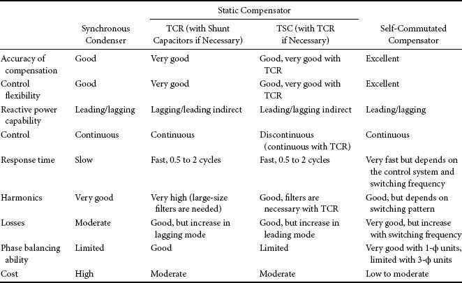
Table 27.1 summarizes the comparative merits of the main types of shunt FACTS compensation. The significant advantages of self-commutated compensators make them an interesting alternative to improve compensation characteristics and also to increase the performance of ac power systems.
As compared with thyristor-controlled capacitor and reactor banks, self-commutated VAR compensators have the following advantages:
1. They can provide both leading and lagging reactive power, thus enabling a considerable saving in capacitors and reactors. This in turn reduces the possibility of resonances at some critical operating conditions.
2. Since the time response of self-commutated converter can be faster than the fundamental power network cycle, reactive power can be controlled continuously and precisely.
3. High frequency modulation of self-commutated converter results in a low harmonic content of the supply current, thus reducing the size of passive filter components.
4. They do not generate inrush current.
5. The dynamic performance under voltage variations and transients is improved.
6. Self-commutated VAR compensators are capable of generating 1 p.u. reactive current even when the line voltages are very low. This ability to support the power system is better than that obtained with thyristor-controlled VAR compensators because the current in shunt capacitors and reactors is proportional to the voltage.
7. Self-commutated compensators with appropriate control can also act as active line harmonic filters, DVR, or UPFC.
Figure 27.21 shows the voltage/current characteristic of a self-commutated VAR compensator compared with that of thyristor-controlled SVC. This figure illustrates that the self-commutated compensator offers better voltage support and improved transient stability margin by providing more reactive power at lower voltages. Because no large capacitors and reactors are used to generate reactive power, the self-commutated compensator provides faster time response and better stability to variations in system impedances.

FIGURE 27.21 Voltage–current characteristics of shunt VAR compensators. (a) Compensator implemented with self-commutated converter (STATCOM). (b) Compensator implemented with back to back thyristors.
27.2.5 Superconducting Magnetic Energy Storage
The principal limitation of STATCOM is that it cannot provide active power, since they have limited energy storage components (dc capacitor or reactor). This limitation is overcome, if the traditional electrolytic capacitor used in the dc link is replaced by an SMES, as shown in Figure 27.22. This device is capable to store and instantaneously discharge large quantities of power [27,28]. It stores energy in the magnetic field created by the flow of dc current in a coil of superconducting material that has been cryo-genically cooled. These systems have been in use for several years to improve power quality and to provide a premium-quality service for individual customers vulnerable to voltage fluctuations. The SMES recharges within minutes and can repeat the charge/discharge sequence thousands of times without any degradation of the magnet. Recharge time can be accelerated to meet specific requirements, depending on system capacity. It is claimed that SMES is 97%–98% efficient and it is much better at providing reactive power on demand. Figure 27.23 shows a different SMES topology using three-level converters.
The first commercial application of SMES was in 1981 [28] along the 500-kV Pacific Intertie, which interconnects California and the Northwest. The device’s purpose was to demonstrate the feasibility of SMES to improve transmission capacity by damping inter-area modal oscillations. Since that time, many studies have been performed and prototypes developed for installing SMES to enhance transmission line capacity and performance. A major cost driver for SMES is the amount of stored energy. Previous studies have shown that SMES can substantially increase transmission line capacity when utilities apply relatively small amounts of stored energy and a large power rating (greater than 50 MW).

FIGURE 27.22 SMES implemented with a 12-pulse thyristor converter.
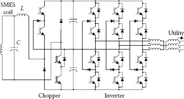
FIGURE 27.23 SMES implemented with a three-level converter.
Another interesting application of SMES for frequency stabilization is in combination with static synchronous series compensator (SSSC) [29].
FACTS controllers can also be of the series type. Typical series compensators use capacitors to reduce the equivalent reactance of a power line at rated frequency, thus increasing the voltage at the load terminals. The connection of a series compensator generates reactive power that, in a self-regulated manner, balances a fraction of the line’s reactance.
27.3.1 Series Compensation Principles
Like shunt compensation, series compensation may also be implemented with current- or voltage-source converters. In this type of compensation, the compensator injects a voltage in series with the load, eliminating voltage unbalance at the load terminals, and supplying the voltage component required to operate with rated, balanced, and constant value. Figure 27.24 shows the principle of series compensation.
Figure 27.25 shows a radial power system, with the reference angle in V2, and the results obtained with the series compensation using a voltage source, which has been adjusted to have unity power factor operation at V2. However, the compensation strategy is different when compared with shunt compensation. In this case, the voltage VCOMP has been added between the line and the load to change the angle of V2, which becomes the voltage at the load terminals. With the appropriate magnitude and phase-shift adjustment of VCOMP, unity power factor can be reached at V2. As can be seen from the phasor diagram of Figure 27.25b, VCOMP generates a voltage phasor with opposite direction to the voltage drop in the line inductance. In this type of compensation, the load current cannot be changed, which means that the compensator voltage must be adjusted to reach the required voltage at the load terminals. Moreover, the amount of apparent power interchanged with the series compensator in this case depends on the VCOMP phase and magnitude. Real and reactive power can be generated from the series compensator, depending on the load and the system requirements. In most cases, series compensation is used to control voltage at the load terminal, so that only reactive power needs to be exchanged. In this case, series capacitors represent a good alternative.

FIGURE 27.24 Three-phase equivalent circuit of a series compensated system.
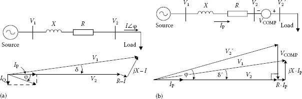
FIGURE 27.25 Principles of series compensation. (a) The radial system without compensation. (b) Series compensation with a voltage source.
Series compensation with capacitors is the most common strategy. Series capacitors are connected with a transmission line as shown in Figure 27.26, which means that all the equipment must be installed on a platform that is fully insulated for the system voltage (both the terminals are at the line voltage). On this platform, the capacitor is located together with overvoltage protection circuits. The overvoltage protection is a key design factor as the capacitor bank has to withstand the throughput fault current, even at a severe fault. The primary overvoltage protection typically involves nonlinear metal-oxide varistors, a spark gap, and a fast bypass switch.
Series compensation is used basically to improve voltage regulation in transmission and distribution power systems. Different compensation equipments using power electronics have been developed to operate as series compensators, as described below.
27.3.2 Static Synchronous Series Compensator
A voltage-source converter can also be used as a series compensator as shown in Figure 27.27. The SSSC injects a voltage in series to the line, 90° phase-shifted with the load current, operating as a controllable series capacitor. The basic difference, as compared with series capacitor, is that the voltage injected by an SSSC is not related to the line current and can be independently controlled [3]. If the phase-shift angle between the injected voltage and the line current is not 90°, active power flows through or from the static compensator. In this case, an energy storage element must be included. This element normally is connected in the dc bus, and modifies the compensator control scheme.
In case of medium voltage application, the SSSC is also known as voltage dynamic restorer, and is used to compensate voltage sag, swells, and unbalance. The principle of operation is similar to the SSSC, but the main difference is that a DVR can compensate active power, since it may be implemented with an energy storage element in the dc bus.
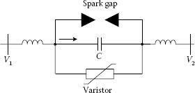
FIGURE 27.26 Series capacitor compensator and associated protection system.
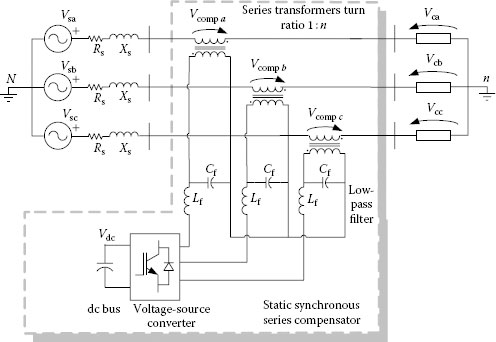
FIGURE 27.27 Static synchronous series compensator (SSSC).
When voltage sags or swells are present at the load terminals, the SSSC responds by injecting three ac voltages in series with the incoming three-phase network voltages, compensating for the difference between faulted and prefault voltages (Figure 27.28). Each phase of the injected voltages can be controlled separately (their magnitude and angle). Active and reactive power required to generate these voltages is supplied by the voltage-source converter, fed from a dc link as shown in Figure 27.28. In order to be able to mitigate voltage sag, the SSSC must present fast control response (Figure 27.28).
Voltage fluctuation at the load terminals can be in magnitude or in phase (or both) as shown in Figure 27.29. When the power supply conditions remain normal the SSSC operate in low-loss standby mode, with the converter side of the booster transformer shorted. Since no voltage-source converter (VSC) modulation takes place, the SSSC produces only conduction losses. In case active power needs to be compensated, an energy storage element must be supplied. This energy storage element is normally connected to the dc bus (supper capacitors, batteries), or the other alternative is to keep the dc capacitor loaded at rated voltage through a noncontrolled rectifier connected to the power line, as shown in Figure 27.30. This is the typical power circuit configuration of a DVR.
27.3.2.1 Compensation Strategies
The magnitude of the compensated voltage can be obtained from the equivalent circuit shown in Figure 27.24, and the phasor diagram shown in Figure 27.20, and is equal to
(27.13) |
(27.14) |
Using complex variables
(27.15) |

FIGURE 27.28 Voltage waveforms using series compensation. (a) Source voltage. (b) Series compensator voltage. (c) Compensated voltage at the load terminals.
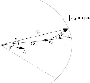
FIGURE 27.29 Phasor diagram for series voltage compensation.
FIGURE 27.30 Power circuit topology of a dynamic voltage restorer (DVR).
The magnitude of the voltage component that must be generated is equal to
(27.16) |
From this expression, different compensation strategies are derived.
27.3.2.1.1 Boosting or In-Phase Compensation
The first compensation strategy is called boosting or in-phase compensation, since the compensated voltage is generated in phase with the load voltage as shown in Figure 27.31. In this case the compensator does not correct the phase-shift introduced at the voltage terminals.
The active and reactive power delivered by the series compensator is given by
(27.17) |
(27.18) |
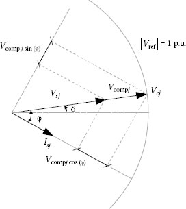
FIGURE 27.31 Phasor diagram of the compensated voltage scheme.
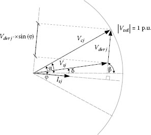
FIGURE 27.32 Phasor diagram of the minimum power injection method.
The in-phase compensation strategy requires the injection of both active and reactive power due to the angle between the compensation voltage and the system current (φ). The active power is taken from the energy storage unit, which defines the ride-through capability of the static series compensator (SSSC or DVR).
27.3.2.1.2 Minimum Power Injection
Unlike the boosting method, the minimum power injection strategy defines an optimal angle for which the compensation voltage Vcomp is 90° phase-shift with the system current, canceling the injection of active power from the series compensator. The limiting factor to compensate the sag only with reactive power is the load power factor. Figure 27.32 illustrates the phasor diagram of the compensation voltage with minimum power injection.
The active power delivered by the series compensator can be obtained from Figure 27.32.
(27.19) |
(27.20) |
(27.21) |
The active power injected by the series compensator, Pcompj, is minimum when the load power factor is equal to 1 (Equation 27.21).
27.3.2.2 Reference Signal Generation
The reference signal is used by the power converter control scheme to generate the required output voltage necessary to keep the load voltage at a given value. Different methods can be used, and the differences are based on the simplicity of implementation, number of calculations, and execution time.
27.3.2.2.1 Pythagoras Method
Based on the Pythagoras theorem, it is possible to generate the signal required to compensate the system voltage drop at the load terminals. This scheme is based on the synchronization of the compensator control signals with the system voltage. The equation used is
(27.22) |
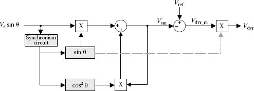
FIGURE 27.33 The block diagram of the Pitagoras algorithm.
The block diagram for the generation of the compensation voltage reference signal for single-phase application is shown in Figure 27.33.
One of the problems that must be taken into consideration during the generation of the compensated voltage reference signal is the sign, which must indicate if the voltage perturbation is a sag or a swell. The type of perturbation defines the polarity of the compensated voltage. If the perturbation is a sag, the compensated voltage must be in phase with the system voltage, but, if the perturbation is a swell, the compensated voltage must be phase-shifted 180° with respect to the equivalent system voltage. The synchronization circuit used to generate the sin θ signal defines the control scheme time response. Different circuits and methods can be used to synchronize the reference signal with the system voltage: zero voltage detector, fast Fourier transform, or phase locked loop. The fastest algorithm is the zero crossing detection, with a time response equal to half a cycle of the system frequency. The Pitagoras method allows the generation of a positive reference signal in case of sag and a negative signal in case of a swell.
27.3.2.2.2 Synchronous Reference Frame
The synchronous reference frame method uses the transformation from the stationary reference frame abc to a dq axes, which are synchronized with the system voltage. The advantage of transforming the voltages from abc to dq is that sinusoidal signals generate continuous signals in dq axis, allowing the use of linear control algorithms. The block diagram of the synchronous reference frame algorithm is shown in Figure 27.34. This scheme generates dc error signals, which are easier to process as compared with the Pitagoras algorithm. Since the system voltages are line to line, in order to transform them in phase to neutral, they must be multiplied by 1/(1 – a2) term.
Another alternative to go from abc to dq axis is to use αβ transformation, as shown in Figure 27.35. In this case, the phase-shift angle θ, used to synchronize the dq axis, is obtained from Equation 27.22.
The principal disadvantage of the indirect algorithm is the presence of a second order harmonic in Vα and Vβ, used to calculate θ. The amplitude of this second order harmonic depends on the voltage unbalance in the abc reference frame. The use of a passive low-pass filter to eliminate the second order harmonic introduces a significant time delay, affecting the transient response of the SSSC. Simulated waveforms showing the characteristics of synchronous reference frame method are shown in Figures 27.36 and 27.37, for a balance and unbalance voltage perturbation.
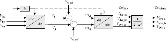
FIGURE 27.34 The block diagram of the synchronous reference frame direct algorithm.

FIGURE 27.35 The block diagram of the synchronous reference frame indirect algorithm.
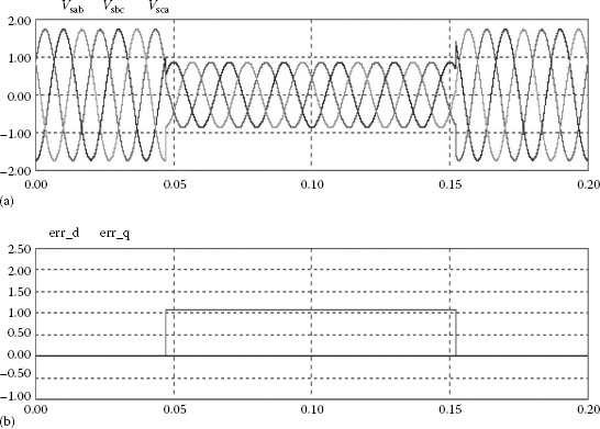
FIGURE 27.36 Simulated voltage waveforms for a balance sag. (a) Line to line system voltage in abc reference frame. (b) Voltage signals in dq axes.
27.3.2.2.3 Sequence Components in Synchronous Reference Frame
Another alternative to generate the reference signal is to use sequence components. From the line voltages in abc frame, the negative, zero, and positive sequence voltage components are calculated:
(27.23) |
The block diagram used to generate the reference signals with the sequence components algorithm is shown in Figure 27.38. The reference voltage signals are phase to neutral, and are calculated from the line to line voltages. By transforming the sequence components from abc to dq reference frame, dc quantities are obtained.

FIGURE 27.37 Simulated voltage waveforms for an unbalance sag. (a) Line to line system voltage in abc reference frame. (b) Voltage signals in dq axes.

FIGURE 27.38 The block diagram of the sequence components algorithm.
If the voltage perturbation is balanced, the reference signals have only positive sequence component, but if the perturbation is unbalanced, positive and negative sequence components are obtained as shown in Figure 27.39.
27.3.2.3 Power Circuit Design
The power circuit topology of the SSSC is composed by the three-phase PWM voltage-source inverter, the second order resonant LC filters, the coupling transformers, and the secondary ripple frequency (Figure 27.27). The main design characteristics for each of the power components are described below.

FIGURE 27.39 Simulated waveforms for an unbalance voltage sag. (a) Unbalanced line to line system voltage in abc reference frame. (b) Positive and negative voltage sequence components in abc reference. (c) Positive and negative sequence reference signal voltages in dq reference frame. (d) Positive and negative sequence reference signal voltages in abc reference frame.
27.3.2.3.1 PWM Voltage-Source Inverter
The rated apparent power required by the inverter can be obtained by calculating the apparent power generated in the primary of the series transformer. The voltage reflected across the primary winding of the coupling transformer is defined by the following expression:
(27.24) |
where
Vseries is the rms voltage across the primary winding of the coupling transformer
K2 is equal to 1
The fundamental component of the primary voltage depends on the amplitude of the negative and positive sequence component of the source-voltage defined by the system voltage regulation and unbalance. The transformer primary current depends on the load.
27.3.2.3.2 Coupling Transformer
The primary windings of the coupling transformers are connected in series to the power system, and as such, they behave as current transformers. The total apparent power required by each series transformer is one-third the total apparent power of the inverter. The turn ratio of the coupling transformer is specified according with the inverter dc bus voltage. The correct value of the turn ratio a must be specified according with the overall SSSC performance. The turn ratio of the coupling transformer must be optimized through the simulation of the overall SSSC, since it depends on the values of different related parameters. In general, the transformer turn ratio must be high in order to reduce the amplitude of the inverter output current and to reduce the voltage induced across the primary winding. Also, the selection of the transformer turn ratio influences the performance of the ripple filter connected at the output of the PWM inverter.
27.3.2.3.3 Secondary Ripple Filter
It is important to note that the design of the secondary ripple filter depends mainly on the coupling transformer turn ratio and on the frequency of the triangular waveform used to generate the inverter gating signals. The ripple filter connected at the output of the inverter avoids the induction of the high frequency ripple voltage generated by the PWM inverter switching pattern at the terminals of the primary windings of the coupling transformers. In this way, the voltage applied in series to the power system corresponds to the components required to compensate voltage unbalance and regulation. The single-phase equivalent circuit of the ripple filter is shown in Figure 27.40.
The voltage reflected to the primary winding of the series transformer has the same waveform as the voltage across the filter capacitor. For low frequency components, the inverter output voltage must be almost equal to the voltage across Cf. However, for high frequency components, most of the inverter output voltage must drop across Lf, in which case the voltage at the capacitor terminals is almost zero. Moreover, Cf and Lf must be selected in order to not exceed the burden of the series transformer. The ripple filter must be designed for the carrier frequency of the PWM voltage-source inverter. To calculate Cf and Lf the system equivalent impedance at the carrier frequency, Zsys, reflected to the secondary must be known. This impedance is equal to
(27.25) |
For the carrier frequency, the following design criteria must be satisfied:
1. XCf ≪ XLf to ensure that at the carrier frequency most of the inverter output voltage will drop across Lf.
2. XCf and XLf ≪ Zsys to ensure that the voltage divider is between Lf and Cf.
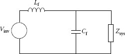
FIGURE 27.40 The single-phase equivalent circuit of the inverter ripple filter.
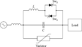
FIGURE 27.41 Power circuit topology of a thyristor-controlled series compensator.
27.3.3 Thyristor-Controlled Series Compensation
Figure 27.41 shows a single line diagram of a thyristor-controlled series compensator (TCSC). TCSC provides a proven technology that addresses specific dynamic problems in transmission systems. TCSCs are an excellent tool to introduce if increased damping is required when interconnecting large electrical systems. Additionally, they can overcome the problem of subsynchronous resonance (SSR), a phenomenon that involves an interaction between large thermal generating units and series compensated transmission systems.
There are two bearing principles of the TCSC concept. First, the TCSC provides electromechanical damping between large electrical systems by changing the reactance of a specific interconnecting power line, i.e., the TCSC will provide a variable capacitive reactance. Second, the TCSC shall change its apparent impedance (as seen by the line current) for subsynchronous frequencies such that a prospective SSR is avoided. Both these objectives are achieved with the TCSC using control algorithms that operate concurrently. The controls will function on the thyristor circuit (in parallel to the main capacitor bank) such that controlled charges are added to the main capacitor, making it a variable capacitor at fundamental frequency but a “virtual inductor” at subsynchronous frequencies.
For power oscillation damping, the TCSC scheme introduces a component of modulation of the effective reactance of the power transmission corridor. By suitable system control, this modulation of the reactance is made to counteract the oscillations of the active power transfer, in order to damp these out.
Static synchronous VAR compensators (STATCOM) and SSSC or DVR can be integrated to get a system capable of controlling the power flow of a transmission line during steady-state conditions and providing dynamic voltage compensation and short circuit current limitation during system disturbances [31].
27.4.1 Unified Power Flow Controller
The UPFC, shown in Figure 27.42, consists of two switching converters operated from a common dc link provided by a dc capacitor, one connected in series with the line and the other in parallel. This arrangement functions as an ideal ac to ac power converter in which the real power can freely flow in either direction between the ac terminals of the two inverters, and each one can independently generate (or absorb) reactive power at its own ac output terminal. The series converter of the UPFC injects via series transformer, an ac voltage with controllable magnitude and phase angle in series with the transmission line. The shunt converter supplies or absorbs the real power demanded by the series converter through the common dc link. The inverter connected in series provides the main function of the UPFC by injecting an ac voltage Vpq with controllable magnitude (0 ≤ Vpq ≤ Vpqmax) and phase angle ρ(0 ≤ ρ ≤ 360°), at the power frequency, in series with the line via a transformer. The transmission line current flows through the series voltage source resulting in real and reactive power exchange between the UPFC and the ac system. The real power exchanged at the ac terminal, i.e., the terminal of the coupling transformer, is converted by the inverter into dc power, which appears at the dc link as positive or negative real power demand. The reactive power exchanged at the ac terminal is generated internally by the inverter.

FIGURE 27.42 UPFC power circuit topology.
The basic function of the inverter connected in parallel (inverter 1) is to supply or absorb the real power demanded by the inverter connected in series to the ac system (inverter 2), at the common dc link. Inverter 1 can also generate or absorb controllable reactive power, if it is desired, and thereby it can provide independent shunt reactive compensation for the line. It is important to note that whereas there is a closed “direct” path for the real power negotiated by the action of series voltage injection through inverter 1 and back to the line, the corresponding reactive power exchanged is supplied or absorbed locally by inverter 2 and therefore it does not flow through the line. Thus, inverter 1 can be operated at a unity power factor or be controlled to have a reactive power exchange with the line independently of the reactive power exchanged by inverter 2. This means that there is no continuous reactive power flow through the UPFC.
27.4.2 Interline Power Flow Controller
An interline power flow controller (IPFC), shown in Figure 27.43, consists of two series voltage-source converters whose dc capacitors are coupled, allowing active power to circulate between different power lines [33]. The IPFC addresses the problem of compensating a number of transmission lines at a given substation. Series capacitive compensators are used to increase the transmittable active power over a given line but they are unable to control the reactive power flow in, and thus the proper load balancing of the line. With the IPFC active power can be transferred between different lines, and therefore it is possible to
1. Equalize both active and reactive power flows between different lines
2. Reduce the burden of the overloaded lines by active power transfer
3. Compensate against resistive line voltage drops and the corresponding reactive power demand
4. Increase the effectiveness of the overall compensating system for dynamic disturbances
In the IPFC the converters do not only provide series reactive compensation but can also be controlled to supply active power to a common dc link from its own transmission line. Like this, active power can be provided from the overloaded lines for active power compensation in other lines. This scheme requires a rigorous maintenance of the overall power balance at the common dc terminal by appropriate control action, allowing that underloaded lines provide appropriate active power transfer to the overloaded ones. When operating below its rated capacity, the IPFC is in regulation mode, allowing the regulation of the active and reactive power flows on one line, and the active power flow on the other line. In addition, the net active power generation by the two coupled converters is zero, neglecting power losses.
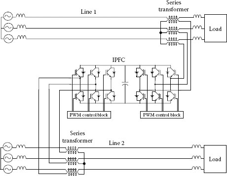
FIGURE 27.43 IPFC power circuit topology.
27.4.3 Unified Power Quality Conditioner
Unlike the previous alternatives, the unified power quality conditioner (UPQC), shown in Figure 27.44, has two main objectives. First, to provide a near sinusoidal and constant voltage to a critical load regardless of the variations (sag, swells, distortion) of the voltage at the ac main terminals in the point of common coupling (PCC). Second, compensate the reactive and/or distorted current taken by the load achieving a near sinusoidal and unity power factor at the PCC. For these reasons, the UPQC is more oriented for load compensation in industrial power distribution systems.

FIGURE 27.44 UPQC power circuit topology.
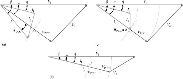
FIGURE 27.45 UPQC phasor’s diagrams. (a) For a general application. (b) For unity power load power factor. (c) For unity system power factor.
The UPQC consists of two PWM converters operated from a common dc voltage link, which must be kept constant. One converter connected in series with the line and the other connected in parallel [31]. The series converter task is to achieve the first objective (clean load voltage) and the parallel converter the second one (sinusoidal current at the system terminals).
The ac voltages of the two converters can be generated with an arbitrary amplitude and phase, thus providing four degrees of freedom. On the other hand, the objectives of achieving a given power factor at the system terminals, a given rms load voltage, and a constant dc link voltage leave one degree of freedom. From the control point of view, this extra degree of freedom could be used to set a given phase-shift between the load voltage and the system voltage. This arbitrary phase angle forces active power to circulate through the dc link of the UPQC. This approach extends the compensating capabilities of the UPQC as compared to null active power circulating through the dc link.
Figure 27.45a shows the general phasor diagram of the UPQC connected to a load with cos ϕ power factor, a system power factor cos θ, a phase-shift angle α between the load and system voltages, a voltage system VPCC (VPCC < V1), and rated voltage V1 at the load side. Figure 27.45b shows that with the UPFC unity power factor can be achieved at the PCC (θPCC = 0). Finally, Figure 27.45c shows that in the case of unity power factor at the PCC, the current Ip can be minimized, therefore the losses at the UPFC are reduced. This operating condition can be achieved if the currents Ii, I1, and Ip are in phase, which is achieved for an α ≠ 0 (unless no sag/swell is present). It is important to note in this case that the active power flowing through the dc link is not zero since the phase-shift angle between the series injected voltage V0 and the supply current Ii is not 90°.
27.5 Facts Controller’s Applications
The implementation of high-performance FACTS controllers enables power grid owners to increase existing transmission network capacity while maintaining or improving the operating margins necessary for grid stability. As a result, more power can reach consumers with a minimum impact on the environment, after substantially shorter project implementation times, and at lower investment costs—all compared to the alternative of building new transmission lines or power generation facilities. Some of the examples of high-performance power system controllers that have been installed and are operating in power systems are described below. Some of these projects have been sponsored by the Electric Power Research Institute (EPRI), based on a research program implemented to develop and promote FACTS.
27.5.1 500 kV Winnipeg–Minnesota Interconnection (Canada–USA) [33]
Northern States Power Co. (NSP) of Minnesota is operating an SVC in its 500 kV power transmission network between Winnipeg and Minnesota. This device is located at Forbes substation, in the state of Minnesota, and is shown in Figure 27.46. The purpose is to increase the power interchange capability on existing transmission lines. This solution was chosen instead of building a new line as it was found superior with respect to increased advantage utilization as well as reduced environmental impact. With the SVC in operation, the power transmission capability was increased in about 200 MW.
The system has a dynamic range of 450 MVAr inductive to 1000 MVAr capacitive at 500 kV, making it one of the largest of its kind in the world. It consists of an SVC and two 500 kV, 300 MVAr mechanically switched capacitor banks (MSC). The large inductive capability of the SVC is required to control the overvoltage during loss of power from the incoming HVDC at the northern end of the 500 kV line.
The SVC consists of two thyristor-switched reactors (TSR) and three TSC. Additionally, the SVC has been designed to withstand brief (<200 ms) overvoltages up to 150% of rated voltage. Without the SVC, power transmission capacity of the NSP network would be severely limited, either due to excessive voltage fluctuations following certain fault situations in the underlying 345 kV system, or due to severe overvoltages at loss of feeding power from HVDC lines coming from Manitoba.
27.5.2 Channel Tunnel Rail Link [31]
Today, it is possible to travel between London and Paris in just over 2 h, at a maximum speed of 300 km/h. The railway power system is designed for power loads in the range of 10 MW. The traction feeding system is a modern 50-Hz, 2–25-kV supply incorporating an autotransformer scheme to keep the voltage drop along the traction lines low. Power step-down from the grid is direct, via transformers connected between two phases. A major feature of this power system, shown in Figure 27.47, is the SVC support. The primary purpose of VAR is to balance the unsymmetrical load and to support the railway voltage in the case of a feeder station trip—when two sections have to be fed from one station. The second purpose of the SVCs is to ensure a low tariff for the active power by maintaining unity power factor during normal operation. Finally, the SVCs alleviate harmonic pollution by filtering the harmonics from the traction load.
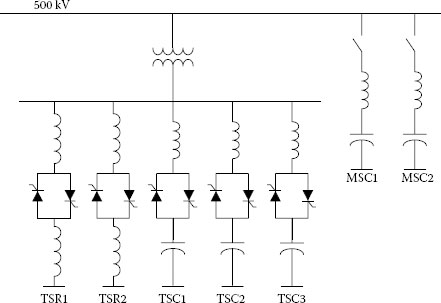
FIGURE 27.46 SVC at the Forbes substation.
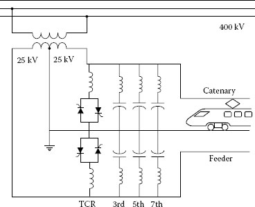
FIGURE 27.47 VAR compensation system for the channel tunnel.
Harmonic compensation is important because strict limits apply to the traction system’s contribution to the harmonic level at the supergrid connection points. The SVCs for voltage support only are connected on the traction side of the interconnecting power transformers. The supergrid transformers for the traction supply have two series-connected medium-voltage windings, each with its midpoint grounded. This results in two voltages, 180° apart, between the winding terminals and ground. The SVCs are connected across these windings; consequently, there are identical single-phase SVCs connected feeder to ground and catenary to ground. The traction load of up to 120 MW is connected between two phases. Without compensation, this would result in an approximately 2% negative phase sequence voltage. To counteract the unbalanced load, a load balancer (an asymmetrically controlled SVC) has been installed in the Sellindge substation. This has a three-phase connection to the grid. The load balancer transfers active power between the phases in order to create a balanced load (as seen by the supergrid).
27.5.3 STATCOM “Voltage Controller” ±100 MVAr STATCOM at Sullivan Substation (TVA) in Northeastern Tennessee [25]
The Sullivan substation is supplied by a 500 kV bulk power network and by four 161 kV lines that are interconnected through a 1200 MVA transformer bank. Seven distributors and one large industrial customer are served from this substation. The STATCOM, shown in Figure 27.48, is implemented with a 48 pulse, two-level voltage-source inverter that combines eight six pulse three-phase inverter bridges, each with a nominal rating of 12.5 MVA, a single step-down transformer having a wye and delta secondary to couple the inverter to the 161 kV transmission line, and a closed-loop liquid cooling system that contains a pumping skid and a fan-cooled, liquid to air heat exchanger unit, a central control system with operator interface. The STATCOM system is housed in one building that is a standard commercial design with metal walls and roof and measured 27.4 × 15.2 m.
The statcom regulates the 161 kV bus voltage during daily load increases to minimize the activation of the tap changing mechanism on the transformer bank, which interconnects the two power systems. The use of this VAR compensator to regulate the bus voltage has resulted in the reduction of the use tap changer from about 250 times per month to 2–5 times per month. Tap changing mechanisms are prone to failure, and the estimated cost of each failure is about $1 million. Without the STATCOM, the transmission company would be compelled either to install a second transformer bank or to construct a fifth 161 kV line into the area; both are costly alternatives.
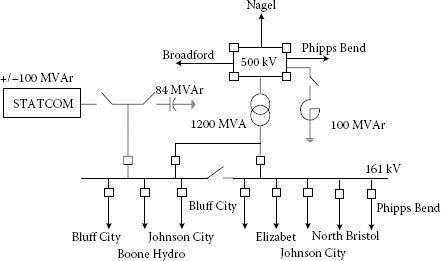
FIGURE 27.48 The 100 MVAr STATCOM at Sullivan substation.
27.5.4 Unified Power Flow Controller “All Transmission Parameters Controller”: ±160 MVA Shunt and ±160 MVA Series at Inez Substation (AEP), Northeastern Virginia, USA [25]
The Inez load area has a power demand of approximately 2000 MW and is served by a long and heavily loaded 138 kV transmission lines. This means that, during normal power delivery, there is a very small voltage stability margin for system contingencies. Single contingency outages in the area will adversely affect the underlying 138 kV system, and in certain cases, a second contingency would be intolerable, resulting in a wide-area blackout. A reliable power supply to the Inez area requires effective voltage support and added real power supply facilities. System studies have identified a reinforcement plan that includes, among other things, the following system upgrades:
1. Construction of a new double-circuit high-capacity 138-kV transmission line from Big Sandy to Inez substation
2. Installation of FACTS controller to provide dynamic voltage support at the Inez substation and to ensure full utilization of the new high-capacity transmission line
The UPFC satisfies all these needs, providing independent dynamic control of transmission voltage as well as real and reactive power flow. The UPFC installation (see Figure 27.49) comprises two identical 3-phase 48-pulse, 160 MVA voltage-source inverters couple to two sets of dc capacitor banks. The two inverters are interfaced with the ac system via two transformers, a set of magnetically coupled windings configured to construct a 48-pulse sinusoidal waveshape. With this arrangement, the following operation modes are possible.
Inverter 1 (connected in parallel) can operate as a STATCOM, with either one of the two main shunt transformers, while inverter 2 (connected in series) operates as an SSSC. Alternatively, inverter 2 can be connected to the spare shunt transformer and operates as an additional STATCOM. With the later configuration, a formidable shunt reactive capability of ±320 MVA would be available, necessary for voltage support at some transmission contingencies in the Inez area. The expected benefits of the installed UPFC are the following:
FIGURE 27.49 Inverter pole assembly of UPFC at Inez substation.
1. Dynamic voltage support at the Inez substation to prevent voltage collapse under double transmission contingency conditions
2. Flexible and independent control of real and reactive power flow on the new high capacity (950 MVA thermal rating) of the 138 kV transmission line
3. Reduction of real power losses by more than 24 MW, which is equivalent to a reduction of CO2 emissions by about 85,000 tons per year
4. More than 100 MW increase in the power transfer and excellent voltage support at the Inez bus
27.5.5 Convertible Static Compensator in the New York 345 kV Transmission System [35]
Convertible Static Compensator (CSC), a versatile and reconfigurable device based on FACTS technology, was designed, developed, tested, and commissioned in the New York 345 kV transmission system. The CSC, shown in Figure 27.50, consists of two 100 MVA voltage-source converters which can be reconfigured and operated as either STATCOM, SSSC, UPFC, or IPFC. The CSC installation at the New York Power Authority’s (NYPA) Marcy 345 kV substation consists of a 200 MVA shunt transformer with two identical secondary windings, and two 100 MVA series coupling transformers for series devices in two 345 kV lines. The CSC provides voltage control on the 345 kV Marcy bus, improved power flow transfers, and superior power flow control on the two 345 kV lines leaving the Marcy substation: Marcy–New Scotland line and Marcy–Coopers Corner line.
Each voltage-source inverter of Figure 27.50 has 12 three-level NPC poles connected to a common dc bus. Inverter pole outputs are connected to an intermediate transformer, which synthesize the 3-phase near-sinusoidal 48-pulse voltage waveform that is coupled into the transmission system.
FIGURE 27.50 One-line diagram of 2 × 100 MVA CSC.
The principles of operation and the actual technological development of different FACTS controllers have been presented and analyzed. Starting from the principles of active, reactive, and voltage compensation, including classical solutions using phase-controlled semiconductors has been reviewed. The introduction of self-commutated topologies based on IGBT and IGCT semiconductors produced a dramatic improvement in the performance of FACTS controllers, since they have a faster dynamic behavior, they can control more variables, and introduce less pollution to power systems. The introduction of new self-commutated topologies at even higher voltage levels will increase the impact of FACTS controllers in future applications.
Some relevant examples of FACTS controllers have been described, where it can be observed that modern compensators improve power systems performance, helping to increase reliability and the quality of power delivered to the customers. These examples show that static power compensators will be used on a much wider scale in the future as grid performance and reliability becomes an even more important factor. Having better grid controllability will allow utilities to reduce investment in the transmission lines themselves. The combination of modern control with real-time information and power electronic technologies will move them very close to their physical limits. Besides, the development of faster and more powerful semiconductor valves will increase in the near future the applicability of FACTS controllers to higher limits.
The authors would like to thank Fondecyt (the Chilean Research Council) for the financial support given through the Projects #105 0067 and #105 0958. The support obtained from Universidad de Concepción, Pontificia Universidad Católica de Chile, and Universidad Federico Santa María is also acknowledged.
1. K. Stahlkopf and M. Wilhelm, Tighter controls for busier systems, IEEE Spectr., 1997, 34(4), 48–52.
2. R. Grünbaum, Å. Petersson, and B. Thorvaldsson, FACTS, improving the performance of electrical grids, ABB Rev., March 2003, 11–18.
3. N. Hingorani and L. Gyugyi, Understanding FACTS, Concepts and Technology of Flexible AC Transmission Systems, IEEE Press, New York, 2000.
4. T. Miller, Reactive Power Control in Electric Systems, John Wiley & Sons, Chichester, U.K., 1982.
5. E. Wanner, R. Mathys, and M. Hausler, Compensation systems for industry, Brown Boveri Rev., 1983, 70, 330–340.
6. G. Bonnard, The problems posed by electrical power supply to industrial installations, Proc. IEE Part B, 1985, 132, 335–340.
7. A. Hammad and B. Roesle, New roles for static VAR compensators in transmission systems, Brown Boveri Rev., 1986, 73, 314–320.
8. N. Grudinin and I. Roytelman, Heading off emergencies in large electric grids, IEEE Spectr., 1997, 34(4), 43–47.
9. C. Taylor, Improving grid behavior, IEEE Spectr., 1999, 36(6), 40–45.
10. R. Grünbaum, M. Noroozian, and B. Thorvaldsson, FACTS—Powerful systems for flexible power transmission, ABB Rev., May 1999, 5, 4–17.
11. Canadian Electrical Association, Static Compensators for Reactive Power Control, Cantext Publications, Winnipeg, Manitoba, Canada, 1984.
12. H. Frank and S. Ivner, Thyristor-controlled shunt compensation in power networks, ASEA J., 1981, 54, 121–127.
13. H. Frank and B. Landstrom, Power factor correction with thyristor-controlled capacitors, ASEA J., 1971, 45(6), 180–184.
14. J. Dixon, Y. del Valle, M. Orchard, M. Ortúzar, L. Morán, and C. Maffrand, A full compensating system for general loads, based on a combination of thyristor binary compensator, and a PWM-IGBT active power filter, IEEE Trans. Ind. Electron., 2003, 50(5), 982–989.
15. S. Torseng, Shunt-connected reactors and capacitors controlled by thyristors, IEE Proc. Part C, 1981, 128(6), 366–373.
16. L. Gyugyi, Reactive power generation and control by thyristor circuits, IEEE Trans. Ind. Appl., 1979, IA-15(5), 521–532.
17. L. Gyugyi, R. Otto, and T. Putman, Principles and applications of static, thyristor-controlled shunt compensators, IEEE Trans. PAS, 1980, PAS-97(5), 1935–1945.
18. A. Chakravorti and A. Emanuel, A current regulated switched capacitor static volt ampere reactive compensator, IEEE Trans. Ind. Appl., 1994, 30(4), 986–997.
19. H. Jin, G. Goós, and L. Lopes, An efficient switched-reactor-based static var compensator, IEEE Trans. Ind. Appl., 1994, 30(4), 997–1005.
20. Y. Sumi, Y. Harumoto, T. Hasegawa, M. Yano, K. Ikeda, and T. Mansura, New static var control using force-commutated inverters, IEEE Trans. PAS, 1981, PAS-100(9), 4216–4223.
21. L. Morán, P. Ziogas, and G. Joos, Analysis and design of a synchronous solid-state VAR compensator, IEEE Trans. Ind. Appl., 1989, IA-25(4), 598–608.
22. J. Dixon, J. García, and L. Morán, Control system for a three-phase active power filter which simultaneously compensates power factor and unbalanced loads, IEEE Trans. Ind. Electron., 1995, 42(6), 636–641.
23. J. Lai and F. Peng, Multilevel converters a new breed of power converters, IEEE Trans. Ind. Appl., 1996, IA-32(3), 509–517.
24. L. Lorenz, Power semiconductors: State of the art and future developments. Keynote Speech at the International Power Electronics Conference, IPEC 2005, Niigata, Japan, April 2005, CD ROM.
25. A. Edris, FACTS technology development: An update, IEEE Power Eng. Rev., March 2000, 20(3), 4–9.
26. S. Bhattacharya, B. Fardenesh, B. Shperling, and S. Zelingher, Convertible static compensator: Voltage source converter based FACTS application in the New York 345 kV transmission system, International Power Electronics Conference, IPEC 2005, Niigata, Japan, April 2005, pp. 2286–2294.
27. M. Superczynski, Analysis of the power conditioning system for a superconducting magnetic energy storage unit, Master’s thesis, Virginia Polytechnic Institute and State University, Blacksburg, VA, August 2000.
28. Reassessment of superconducting magnetic energy storage (SMES) transmission system benefits, Report number 01006795, March 2002.
29. I. Ngamroo, Robust frequency stabilization by coordinated superconducting magnetic energy storage with static synchronous series compensator, Int. J. Emerg. Electr. Power Syst., 2005, 3(1), 16–25.
30. C. Sepúlveda, J. Espinoza, and R. Ortega, Analysis and design of a linear control strategy for three-phase UPQCs, Conference Record of IECON’04, Busan, Korea, November 3–6, 2004.
31. R. Grünbaum, Å. Petersson, and B. Thorvaldsson, FACTS improving the performance of electrical grids, ABB Rev., Special Report on Power Technologies, 2003, 13–18.
32. J. Dixon and L. Morán, A clean four-quadrant sinusoidal power rectifier, using multistage converters for subway applications, IEEE Trans. Ind. Electron., 2005, 52(3), 653–661.
33. X. Wei, J. Chow, B. Fardanesh, and A. Edris, A dispatch strategy for an interline power flow controller operating at rated capacity, PSCE 2004, 2004 IEEE/PES Power Systems Conference and Exposition, New York, October, pp. 10–13, 2004.
34. C. Luongo, Superconducting storage systems: An overview, IEEE Trans. Magn., 1996, 32(4), 2214–2223.
35. K. Sen, Recent developments in electric power transmission technology, The Carnegie Mellon Electricity Industry Center, EPP Conference room, April 15, 2003 (http://wpweb2.tepper.cmu.edu/ceic/SeminarPDFs/Sen_CEIC_Seminar_4_15_03.pdf).