Voltage Regulators and Power Supplies
Circuits usually require a dc power supply that can maintain a fixed voltage while supplying enough current to drive a load. Batteries make good dc supplies, but their relatively small current capacities make them impractical for driving high-current, frequently used circuits. An alternative solution is to take a 120-V ac, 60-Hz line voltage and convert it into a usable dc voltage.
There are two approaches to this. The more traditional approach is to use a step-down transformer. The other approach is to use a “switch-mode” power supply. This latter method has all but taken over from step-down transformers in recent years, and is the reason your “wall-wart” black plastic power adapters have become smaller and lighter. They also have the advantage that they will often work without modification or switch flipping on the higher line voltages found in other parts of the world. We’ll discuss both methods in this chapter, beginning with the step-down transformer approach.
The trick to converting the ac line voltage into a usable (typically lower-level) dc voltage is to first use a transformer to step down the ac voltage. After that, the transformed voltage is applied through a rectifier network to get rid of the negative swings (or positive swings if you are designing a negative voltage supply). Once the negative swings are eliminated, a filter network is used to flatten out the rectified signal into a nearly flat (rippled) dc voltage pattern. Figure 11.1 shows the process in action.

FIGURE 11.1
Now there is one problem with this supply—it is unregulated. This means that if there are any sudden surges within the ac input voltage (spikes, dips, etc.), these variations will be expressed at the supply’s output (notice the spike that gets through in Fig. 11.1). Using an unregulated supply to run sensitive circuits (e.g., digital IC circuits) is a bad idea. The current spikes can lead to improper operating characteristics (e.g., false triggering, etc.) and may destroy the ICs in the process. An unregulated supply also has a problem maintaining a constant output voltage as the load resistance changes. If a highly resistive (low-current) load is replaced with a lower-resistance (high-current) load, the unregulated output voltage will drop (Ohm’s law).
Fortunately, there is a special circuit that can be placed across the output of an unregulated supply to convert it into a regulated supply—a supply that eliminates the spikes and maintains a constant output voltage with load variations (see Fig. 11.2). This special circuit is called a voltage regulator.

FIGURE 11.2
A voltage regulator is designed to automatically adjust the amount of current flowing through a load—so as to maintain a constant output voltage—by comparing the supply’s dc output with a fixed or programmed internal reference voltage. A simple regulator consists of a sampling circuit, an error amplifier, a conduction element, and a voltage reference element (see Fig. 11.3).

FIGURE 11.3
The regulator’s sampling circuit (voltage divider) monitors the output voltage by feeding a sample voltage back to the error amplifier. The reference voltage element (zener diode) acts to maintain a constant reference voltage that is used by the error amplifier. The error amplifier compares the output sample voltage with the reference voltage and then generates an error voltage if there is any difference between the two. The error amplifier’s output is then fed to the current-control element (transistor), which is used to control the load current.
In practice, you do not have to worry about designing voltage-regulator circuits from scratch. Instead, what you do is spend 50 cents for a voltage-regulator IC. Let’s take a closer look at these integrated devices.
11.1 Voltage-Regulator ICs
There are a number of different kinds of voltage-regulator ICs on the market today. Some of these devices are designed to output a fixed positive voltage, some are designed to output a fixed negative voltage, and others are designed to be adjustable.
11.1.1 Fixed Regulator ICs

One popular line of regulators includes the three-terminal LM78xx series shown here. The “xx” digits represent the output voltage, e.g., 7805 (5 V), 7806 (6 V), 7808 (8 V), 7810 (10 V), 7812 (12 V), 7815 (15 V), 7818 (18 V), and 7824 (24 V). These devices can handle a maximum output current of 1.5 A if properly heat-sunk. To remove unwanted input or output spikes/noise, capacitors can be attached to the regulator’s input and output terminals, as shown in the figure. A popular series of negative voltage-regulator IC is the LM79xx regulators, where “xx” represent the negative output voltage. These devices can handle a maximum output current of 1.5 A. A number of different manufacturers make their own kinds of voltage regulators. Some of the regulators can handle more current than others.
These devices are also available as SMD parts, typically in a SOT-89 package. Be sure to check the data sheets though, as these parts often have a lower maximum output current than their through-hole siblings.
Check out the catalogs to see what is available.
FIGURE 11.4

The LM317 regulator shown here is a popular 3-terminal adjustable positive voltage regulator. Unlike the 7800 fixed voltage-regulator series, the LM317 is a floating regulator—it sees only the input-to-output differential voltage—and it can be programmed via two external resistors to set the output voltage. In operation, the LM317 develops a nominal 1.25 V reference voltage between the output and adjust terminals. This reference voltage is impressed across program resistor R1, and since this voltage is constant, a constant current I1 flows through the output set resistor R2, giving an output voltage given by the equation shown in the figure. Increasing R2 forces the regulator’s output to a higher level. The LM317 is designed to accept an unregulated input voltage of up to 37 V and can output a maximum current of 1.5 A. The TL783 is another positive adjustable regulator that can output a regulated voltage of from 1 to 125 V, with a maximum output current of 700 mA. The LM337T, unlike the previous two regulators, is an adjustable negative voltage regulator. It can output a regulated voltage of from –1.2 V to –37 V, with a maximum output current of 1.5 A. Again, check the electronics catalogs to see what other kinds of adjustable regulators are available. (Cin should be included if the regulator is far from the power source; it should be around 0.1 μF or so. Cout is used to eliminate voltage spikes at the output; it should be around 0.1 μF or larger.)
FIGURE 11.5
11.1.3 Regulator Specifications
The specifications tables for regulators typically will provide you with the following information: output voltage, accuracy (percent), maximum output current, power dissipation, maximum and minimum input voltage, 120-Hz ripple rejection (decibels), temperature stability (ΔVout/ΔT), and output impedance (at specific frequencies). A regulator’s ripple rejection feature can greatly reduce voltage variations in a power supply’s output, as you will discover later in this chapter.
11.2 A Quick Look at a Few Regulator Applications
Before we take a look at how voltage regulators are used in power supplies, it is worthwhile seeing how they are used in other types of applications. Here are a few examples.
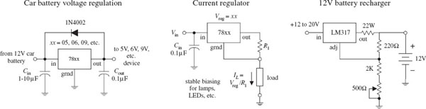
FIGURE 11.6
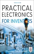
The constant current regulator is often used as a power supply for LEDs, especially the higher-power devices.
11.3 The Transformer
It is important that you choose the right transformer for your power supply. The transformer’s secondary voltage should not be much larger than the output voltage of the regulator; otherwise, energy will be wasted because the regulator will be forced to dissipate heat. However, at the same time, the secondary voltage must not drop below the required minimum input voltage of the regulator (typically 2 to 3 V above its output voltage).
11.4 Rectifier Packages
Three basic rectifier networks used in power supply designs include the half-wave, full-wave, and bridge rectifiers, shown in Fig. 11.7. To understand how these rectifiers work, see Chap. 4.

FIGURE 11.7
Half-wave, full-wave, and bridge rectifiers can be constructed entirely from individual diodes. However, both full-wave and bridge rectifiers also come in preassembled packages (see Fig. 11.8).
FIGURE 11.8
Make sure that the power supply’s rectifier diodes have the proper current and peak-inverse-voltage (PIV) ratings. Typical rectifier diodes have current ratings from 1 to 25 A, PIV ratings from 50 to 1000 V, and surge-current ratings from around 30 to 400 A. Popular general-purpose rectifier diodes include the 1N4001 to 1N4007 series (rated at 1 A, 0.9-V forward voltage drop), the 1N5059 to 1N5062 series (rated at 2 A, 1.0-V forward voltage drop), the 1N5624 to 1N5627 series (rated at 5 A, 1.0-V forward voltage drop), and the 1N1183A-90A (rated at 40 A, 0.9-V forward voltage drop). For low-voltage applications, Schottky barrier rectifiers can be used; the voltage drop across these rectifiers is smaller than a typical rectifier (typically less than 0.4 V); however, their breakdown voltages are significantly smaller. Popular full-wave bridge rectifiers include the 3N246 to 3N252 series (rated at 1 A, 0.9-V forward voltage drop) and the 3N253 to 3N259 series (rated at 2 A, 0.85-V forward voltage drop).
11.5 A Few Simple Power Supplies
Regulated +5-V Supplies
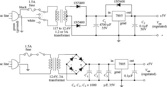
The first supply uses a center-tapped transformer rated at 12.6 V at 1.2 to 3 A. The voltage after rectification resides at an 8.9-V peak pulse. The filter capacitor (C1) smoothes the pulses, and the 7805 outputs a regulated +5 V. C2 is placed across the output of the regulator to bypass high-frequency noise that might be generated by the load. The diode placed across the 7805 helps protect the regulator from damaging reverse-current surges generated by the load. Such surges may result when the power supply is turned off. For example, the capacitance across the output may discharge more slowly than the capacitance across the input. This would reverse-bias the regulator and could damage it in the process. The diode diverts the unwanted current away from the regulator. The second power supply is similar to the first but uses a bridge rectifier.
FIGURE 11.9

FIGURE 11.10a This dual-polarity linear power supply will provide any positive or negative voltage between 1.2 and 35 V. The complementary regulators—LM317 (+) and LM337 (−)—can deliver up to 1.5 A (output voltage dependent) if provided adequate heat sinking. This is sufficient for testing or powering a wide variety of everyday circuits. The key is the center-tap transformer with secondary tapped to ground that supplies both positive and negative voltages relative to ground. It converts the line voltage from 120 VAC to 48 VAC at the secondary, which is center-tapped and divided into 24-VAC portions. By using the center tap as a ground or common connection, it is possible to get both positive and negative outputs relative to ground. The diodes rectify the ac from the transformer output into a pulsing dc waveform. C1 and C2 electrolytic capacitors perform bulk filtering of the pulsing dc waveform, resulting in a raw dc voltage. C3 and C4 are small film capacitors bypassing the electrolytic capacitors to improve transient response and filter high-frequency line noise. The LM317 (+) and LM337 (−) are complementary adjustable voltage regulators, whose output can be programmed with two external resistors. The output voltage is given by:
C5 and C6 improve the regulators’ ripple rejection from 65 dB to 80 dB by preventing ripple voltage from being amplified at the output of the regulator. C7 and C8 electrolytic capacitors stiffen the output voltage and reduce output impedance. C9 and C10 are small bypass capacitors to filter any high-frequency noise present at the output. All bypass capacitors should have low impedance (e.g., polyester, polypropylene, polystyrene, or Mylar film capacitors are okay). A 48-VAC CT (24-0-24) transformer is about the practical upper limit of commonly available models. This limit is set by the maximum input voltage of the regulators, and also by the bulk filter capacitors that are rated at 35 VDC.

Here, a 7815 positive voltage regulator and a 7915 negative voltage regulator are used to construct a ±15-V supply.
FIGURE 11.10b

FIGURE 11.10c Here’s a fixed +/-12 V made by using a center-tap 18-VAC transformer, a full-wave rectifier, and 7812 and 7912 regulators. This circuit is particularly useful when powering op amp circuits.

This figure shows a simple way to add an external dc power supply input to a battery-powered device. With no external power (external dc adapter plug not connected), the shorting jack acts to switch power to the battery. However, when external dc power is applied via a dc adapter plug, the shorting jack switches power from the battery to the dc adapter connects.
FIGURE 11.11
11.6 Technical Points About Ripple Reduction
When using a supply to power sensitive circuits, it is essential to keep the variation in output voltage as small as possible. For example, when driving digital circuits from a 5-V supply, the variation in output voltage should be no more than 5 percent, or 0.25 V, if not lower. In fact, digital logic circuits usually have a minimum 200-mV noise margin around critical logic levels. Small analog signal circuits can be especially finicky when it comes to output variations. For example, they may require a variation less than 1 percent to operate properly. How do you keep the output variation error low? You use filter capacitors and voltage regulators.
Filter capacitors act to reduce the fluctuations in output by storing charge during the positive-going rectifier cycle and then releasing charge through the load—at a slow enough rate to maintain a level output voltage—during the negative-going rectifier cycle. If the filter capacitor is too small, it will not be able to store enough charge to maintain the load current and output voltage during the negative-going cycle.
As it turns out, the amount of current drawn by a load influences the rate of capacitor discharge. If a low-resistance, high-current load is placed across the supply’s output, the capacitor will discharge relatively quickly, causing the voltage across the capacitor and therefore the voltage across the load to drop relatively quickly. On the other hand, a highly resistive, low-current load will cause the capacitor to discharge more slowly, which means the dip in output voltage will not be as significant. To calculate the drop in voltage of the capacitor during its discharge cycle, use
where I is the load current, Δt is the discharge time, and ΔV is the fluctuation in output above and below the average dc level. ΔV is also referred to as the peak-to-peak ripple voltage Vripple(pp). (Here, I cheated by substituting straight lines for exponential decays to describe the discharge cycle; see Fig. 11.12.) Δt can be approximated by dividing 1 by the rectified output voltage frequency. For a full-wave rectifier, the period is 1/120 Hz, or 8.3 × 10⁻³ s. In reality, the actual amount of time the capacitor spends discharging during a peak-to-peak variation is about 5 ms. The other 3.3 ms is used up during the charge. To make life easier on you, the following equation simplifies matters:
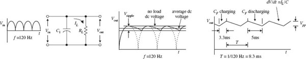
FIGURE 11.12
Note that the ripple voltage is not given in the peak-to-peak form but is given in the rms form (recall that Vpp =  Vrms). To test the equation out, let’s find the ripple voltage for a 5-V supply that has a 4700-μF filter capacitor and a maximum load current of 1.0 A. (Here I am pretending that no voltage regulator is present at this point.) After plugging the numbers into the equation, you get Vripple(rms) = 510 mV. But now, recall that a minute ago I said that the amount of variation in the output had to be ±0.25 V% to run digital ICs—510 mV is too big. Now you could keep fiddling around with the capacitance value in the equation and come up with an even better answer, say, letting C equal infinity. In theory, this is fine, but in reality, it is not fine. It is not fine for three basic reasons. The first reason has to do with the simple fact that you cannot find a capacitor at Radio Shack that has an infinite capacitance. If an infinite-capacitance capacitor existed, the universe would not be the same, and you and I probably would not be around to talk about it. The second reason has to do with capacitor tolerances. Unfortunately, the high-capacity electrolytic capacitors used in power supplies have some of the worst tolerances among the capacitor families. It is not uncommon to see a 5 to 20 percent or even larger percentage tolerance for these devices. The mere fact that the tolerances are so bad makes being “nitpicky” about the equation a questionable thing to do. The third and perhaps most important reason for avoiding fiddling around with the equation too much has to do with the inherent ripple-rejection characteristics of voltage regulators. As you will see, the voltage regulator can save us.
Voltage regulators often come with a ripple-rejection parameter given in decibels. For example, the 7805 has a ripple-rejection characteristic of about 60 dB. Using the attenuation expression, you can find the extent of the ripple reduction:

The last expression says that the output ripple is reduced by a factor of 1000. This means that if you use the regulator with the initial setup, you will only have an output ripple of 0.51 mV—a value well within the safety limits. At this point, it is important to note that the 7805 requires a minimum voltage difference between its input and output of 3 V to function properly. This means that to obtain a 5-V output, the input to the regulator must be at least 8 V. At the same time, it is important to note the voltage drop across the rectifier (typically around 1 to 2 V). The secondary voltage from the transformer therefore should be even larger than 8 V. A transformer with a secondary voltage of 12 V or so would be a suitable choice for the 5-V supply.
Now let’s see how well the LM319 adjustable regulator rejects the ripple. Let’s say that an LM317 is used in a power supply that has a transformer secondary rms voltage of 12.6 V. The capacitor’s peak voltage during a cycle will be 17.8 V (the peak-to-peak voltage of the secondary). An LM317 has a ripple-rejection characteristic of around 65 dB, but this value can be raised to approximately 80 dB by bypassing the LM317’s voltage divider with a 10-μF capacitor (see Fig. 11.13).
FIGURE 11.13
If you let C = 4700 μF and assume a 1.5-A maximum load current, you get a ripple voltage of
Vr(rms) = 0.0024 s(1.5 A/4700 μF) = 760 mV
Again, the ripple voltage is too much for sensitive ICs to handle. However, if you consider the LM319’s ripple-rejection characteristic (assuming that you use the bypassing capacitor), you get a reduction of

In other words, the output ripple is reduced by a factor of 10,000, so the final output ripple voltage is only 0.076 mV.
11.7 Loose Ends
Line Filter and Transients Suppressors
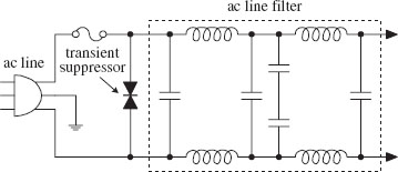
A line filter is an LC filter circuit that is inserted into a supply to filter out unwanted high-frequency interference present in the input line supply. Line filters also can help reduce voltage spikes, as well as help eliminate the emission of radiofrequency interference by the power supply. Line filters are placed before the transformer, as shown in the figure. AC line filters can be purchased in preassembled packages. See the electronics catalogs for more info.
A transient suppressor is a device that acts to short out when the terminal voltage exceeds safe limits (e.g., spikes). These devices act like bidirectional high-power zener diodes. They are inexpensive, come in diode-like packages, and come with low-voltage and peak-pulse-voltage ratings.
FIGURE 11.14

The crowbar and clamp circuits shown here can be placed across the output of a regulated supply to protect a load against an unregulated voltage that would be present at the output if the voltage regulator failed (shorted internally).
CROWBAR
For the crowbar circuit, when the supply voltage exceeds the zener diode’s breakdown voltage by 0.6 V, the zener diode conducts, triggering the SCR into conduction. The SCR then diverts potentially harmful current to ground. The crowbar’s SCR will not turn off until the power supply is turned off or the SCR’s anode-to-cathode current is interrupted, say, by means of a switch.
CLAMP
A zener diode placed across the output of a supply also can be used for overvoltage protection. However, it may “fry” if the unregulated current is too large. To avoid frying the zener diode, use a high-power transistor to help divert the current. When the zener diode’s breakdown voltage is exceeded, some of the current that flows through it will enter the transistor’s base, allowing the excessive current to flow toward ground. Using clamps can eliminate false triggering caused by voltage spikes; the crowbar, on the other hand, would need to be reset in such a case.
FIGURE 11.15
Bleeder Resistors and Transient Suppressors

When a resistor is placed across the output of the unregulated supply, it will act to discharge the high-voltage (potentially lethal) filter capacitor when the supply is turned off and the load removed. Such a resistor is referred to as a bleeder resistor. A 1-k, 1/2-W resistor is suitable for most applications.
An RC network placed across the primary coil of the transformer can prevent large, potentially damaging inductive transients from forming when the supply is turned off. The capacitor must have a high voltage rating. A typical RC network consists of a 100-Ω resistor and a 0.1-µF, 1-kV capacitor. Special z-lead transient suppressor devices can also be used, as was mentioned earlier.
FIGURE 11.16
11.8 Switching Regulator Supplies (Switchers)
A switching power supply, or switcher, is a unique kind of power supply that can achieve power conversion efficiencies far exceeding those of the linear supplies covered earlier in this chapter. With linear regulated supplies, the regulator converts the input voltage that is higher than needed into a desired lower output voltage. To lower the voltage, the extra energy is dissipated as heat from the regulator’s control element. The power-conversion efficiency (Pout/Pin) for these supplies is typically lower than 50 percent. This means that more than half the power is dissipated as heat.
Switchers, on the other hand, can achieve power-conversion efficiencies exceeding 85 percent, meaning that they are much more energy efficient than linearly regulated supplies. Switchers also have a wide current and voltage operating range and can be configured in either step-down (output voltage smaller than input voltage), step-up (output voltage larger than input voltage), or inverting (output is the opposite polarity of the input) configurations. Also, switchers can be designed to run directly off ac line power, without the need for a power transformer. By eliminating the hefty power transformer, the switcher can be made light and small. This makes switchers good supplies for computers and other small devices.
A switching supply resembles a linear supply in many ways. However, two unique features include an energy-storage inductor and a nonlinear regulator network. Unlike a linear supply, which provides regulation by varying the resistance of the regulator’s control element, a switcher incorporates a regulation system in which the control element is switched on and off very rapidly. The on/off pulses are controlled by an oscillator/error amplifier/pulse-width modulator network (see Fig. 11.17).

FIGURE 11.17
During the on cycle, energy is pumped into the inductor (energy is stored in the magnetic fields about the inductor’s coil). When the control element is turned off, the stored energy in the inductor is directed by the diode into the filter and into the load. The sampling circuit (R2 and R3) takes a sample of the output voltage and feeds the sample to one of the inputs of the error amplifier. The error amplifier then compares the sample voltage with a reference voltage applied to its other input. If the sample voltage is below the reference voltage, the error amplifier increases its output control voltage. This control voltage is then sent to the pulse-width modulator. (If the sample voltage is above the reference voltage, the error amplifier will decrease the output voltage it sends to the modulator.) While this is going on, the oscillator is supplying a steady series of triggering voltage pulses to the pulse-width modulator. The modulator uses both the oscillator’s pulses and the error amplifier’s output to produce a modified on/off signal that is sent to the control element’s base. The modified signal represents a squarewave whose on time is determined by the input error voltage. If the error voltage is low (meaning the sample voltage is higher than it should be), the modulator sends a short-duration on pulse to the control element. However, if the error voltage is high (meaning the sample voltage is lower than it should be), the pulse-width modulator sends a long-duration on pulse to the control element. (The graph in Fig. 11.17 shows how the oscillator, error amplifier, and pulse-width modulator outputs are related.) Using a series of on/off pulses that can be varied in frequency and duration gives the switching regulator its exceptional efficiency; releasing a series of short pulses of energy over time is more efficient than taking excessive supply energy and radiating it off as heat (linear supply).
Figure 11.18 shows a typical switching regulator arrangement. The 556 dual-timer IC houses both the oscillator and pulse-width modulator, while the UA723 voltage-regulator IC acts as the error amplifier. R2 and R3 comprise the sampling network, R6 and R7 set the reference voltage, and R4 and R5 set the final control voltage that is sent to the pulse-width modulator.

FIGURE 11.18
Step-Up, Step-Down, and Inverting Configurations
The switching regulator in Fig. 11.17 is referred to as a step-down regulator. It is used when the regulated output voltage is to be lower than the regulator input voltage. Now, switching regulators also come in step-up and inverting configurations. The step-up version is used when the output is to be higher than the input, whereas the inverting version is used when the output voltage is to be the opposite polarity of the input voltage. Here’s an overview of the three configurations.
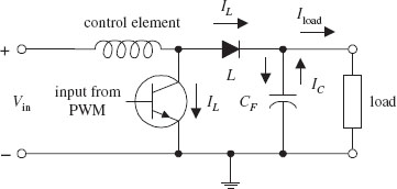
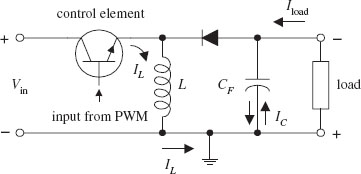
STEP-DOWN REGULATOR

This is used when output voltage is to be lower than input voltage. When the control element is on, L stores energy, helps supply load current, and supplies current to the filter capacitor. When the control element is off, the energy stored in L helps supply load current but again restores charge on CF—the charge on CF is used to supply the load when the control element turns off and L has discharged its energy.
FIGURE 11.19
STEP-UP SWITCHER REGULATOR
This is used when output is to be higher than input voltage. When the control element is on, energy is stored in the inductor. The load, isolated by the diode, is supplied by the charge stored in CF. When the control element is off, the energy stored in L is added to the input voltage. At the same time, L supplies load current, as well as restoring the charge on CF—the charge on CF is used to supply the load current when the control element is off and when the energy in L is discharged.
FIGURE 11.20
This is used when output voltage is to be the opposite polarity of the input voltage. When the control element is on, energy is stored in L, while the diode isolates L from load. The load current is supplied by the charge on CF. When the control element is turned off, the energy stored in L charges CF to a polarity such that Vout is negative. IL supplies load current and restores the charge on CF while it is discharging its energy. CF supplies load current when the control element is off and the inductor is discharged. An inverting switcher regulator can be designed to step up or step down the inverted output.
FIGURE 11.21
11.9 Switch-Mode Power Supplies
The logical extension of a switching regulator is to ditch the transformer entirely and work directly from rectified line voltage.
Transformer-based designs have become a rare occurrence in consumer electronics. Transformers are relatively expensive and heavy components. Watt for watt, a switch-mode power supply is generally cheaper to produce.
By using the unique switching action of the switcher, it is possible to design a supply that does not require the hefty 60-Hz power transformer at the input stage. In other words, you can design a switching power supply to run directly off a 120-V ac line—you still must rectify and filter the line voltage before feeding it to the regulator. However, if you remove the power transformer, you remove the protective isolation that is present between the 120-V ac line and the dc input to the supply. Without the isolation, the dc input voltage will be around 160 V. To avoid this potentially “shocking” situation, the switching regulator must be modified. One method for providing isolation involves replacing the energy-storage inductor with the secondary coil of a high-frequency transformer while using another high-frequency transformer or optoisolator to link the feedback from the error amplifier to the modulating element (see Fig. 11.22).

FIGURE 11.22
Now, you may be wondering how removing one transformer and adding another transformer (if not two) makes things smaller and lighter. Well, according to the laws of physics, as the frequency of an alternating signal increases, the need for a large iron core within the transformer decreases. You can use the high-frequency transformer(s) because the switcher’s oscillator is beating so fast (e.g., 65 kHz). The difference in size and weight between a switching supply that uses high-frequency transformers and a supply that uses a 60-Hz power transformer is significant. For example, a 500-W switching supply takes up around 640 in3 as compared with 1520 in3 for a linear supply rated at the same power. Also, switching supplies run cooler than linear supplies. In terms of watts per cubic inch, a switching power supply can achieve 0.9 W/in3, while a linear supply usually provides 0.4 W/in3.
There is a slight problem with switchers that should be noted. As a result of the on/off pulsing action of the switching regulator, a switching supply’s output will contain a small switching ripple voltage (typically in the tens of millivolts). Usually the ripple voltage does not pose too many problems (e.g., 200-mV noise margins for most digital ICs are not exceeded). However, if a circuit is not responding well to the ripple, an external high-current, low-pass filter can be added.
11.10 Kinds of Commercial Power Supply Packages
To make life easier, you can forget about designing your own supplies and buy one that has been made by the pros. These supplies come in either linear or switcher form and come in a variety of different packages. Here are some of the packages that are available.
Small Modular Units
These are used in low-power applications (e.g., ±5, ±10, ±15 V). Supplies are housed in small modules, usually around 2.5 × 3.5 × 1 in. They often come with pinlike leads that can be mounted directly into circuit boards or come with terminal-strip screw connections along their sides. These supplies may come with single (e.g., +5 V), dual (e.g., ±15 V), or triple (e.g., +5 V, ±15 V) output terminals. Linear units have power ratings from around 1 to 10 W, while switching units have power ratings from around 10 to 25 W. You must supply the fuses, switches, and filters.
FIGURE 11.23
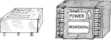
Open Frame
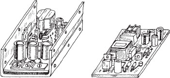
This supply’s circuit board, transformer, etc. are mounted on a metal platform (if it is a low-voltage supply, it may simply be mounted on a circuit board) that is inserted into an instrument. These supplies come in linear and switching types and come with a wide range of voltage, current, and power ratings (around 10 to 200 W for linear supplies, 20 to 400 W for switching supplies). You will probably have to supply the fuses, switches, and filters.
FIGURE 11.24
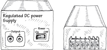
These supplies are enclosed in a metal box that is especially designed to efficiently radiate off excessive heat. They come in both linear and switching forms. Power rating ranges from around 10 to 800 W for linear supplies and 20 to 1500 W for switching supplies.
FIGURE 11.25
Wall Plug-In
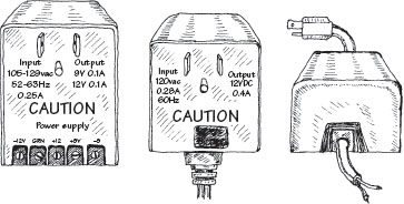
Wall plug-in power supplies (often called "wall-warts") get inserted directly into an ac wall socket. Some of these devices only provide ac transformation, others supply an unregulated dc voltage, and others supply a regulated dc output. Typical output voltages include +3, +5, +6, +7.5, +9, +12, and +15 V. They also come in dual-polarity form.
These devices are mostly switched mode, and are manufactured in millions, as they are not specific to a product. They are small and light, and it is possible to get a unit that can supply 2 A at 12 V at a cost of less than $10.
This approach is helped by the largely standard 6.3 mm plug for the dc voltage, which, in most consumer appliances, has a positive inner connection and a negative outer sheath connection. Note that this is often the other way around in musical equipment, such as guitar effects pedals.
FIGURE 11.26
11.11 Power Supply Construction
When building a power supply, the following suggestions should help:
FIGURE 11.27
• Mount the transformer directly to the metal enclosure box, toward the rear.
• Install fuses, power switch, and binding posts at the rear of the box.
• Mount circuit boards on standoffs within the box.
• Place diode or rectifier modules, along with the capacitors and voltage regulators, on the circuit board.
• Make sure to heat-sink voltage regulators.
• Place supply output jacks on the front of the box.
• Drill holes in box to allow cooling.
• Ground the box.
• Place the power-line core through a hole in the rear. Use a rubber grommet for strain relief.
• To avoid shocks, make sure to insulate all exposed 120-V power connections inside the box with heat-shrink tubing.
..................Content has been hidden....................
You can't read the all page of ebook, please click here login for view all page.