
Oscillators and Timers
Within practically every electronic instrument there is an oscillator of some sort. The task of the oscillator is to generate a repetitive waveform of desired shape, frequency, and amplitude that can be used to drive other circuits. Depending on the application, the driven circuit(s) may require either a pulsed, sinusoidal, square, sawtooth, or triangular waveform.

FIGURE 10.1
In digital electronics, squarewave oscillators, called clocks, are used to drive bits of information through logic gates and flip-flops at a rate of speed determined by the frequency of the clock. In radio circuits, high-frequency sinusoidal oscillators are used to generate carrier waves on which information can be encoded via modulation. The task of modulating the carrier also requires an oscillator. In oscilloscopes, a sawtooth generator is used to generate a horizontal electron sweep to establish the time base. Oscillators are also used in synthesizer circuits, counter and timer circuits, and LED/lamp flasher circuits. The list of applications is endless.
The art of designing good oscillator circuits can be fairly complex. There are a number of designs to choose from and a number of precision design techniques required. The various designs make use of different timing principles (e.g., RC charge/discharge cycle, LC resonant tank networks, crystals), and each is best suited for use within a specific application. Some designs are simple to construct but may have limited frequency stability. Other designs may have good stability within a certain frequency range, but poor stability outside that range. The shape of the generated waveform is obviously another factor that must be considered when designing an oscillator.
This chapter discusses the major kinds of oscillators, such as the RC relaxation oscillator, the Wien-bridge oscillator, the LC oscillator, and the crystal oscillator. The chapter also takes a look at popular oscillator ICs.
Perhaps the easiest type of oscillator to design is the RC relaxation oscillator. Its oscillatory nature is explained by the following principle: Charge a capacitor through a resistor and then discharge it when the capacitor voltage reaches a certain threshold voltage. After that, the cycle is repeated, continuously. In order to control the charge/discharge cycle of the capacitor, an amplifier wired with positive feedback is used. The amplifier acts like a charge/discharge switch—triggered by the threshold voltage—and also provides the oscillator with gain. Figure 10.2 shows a simple op amp relaxation oscillator.

Assume that when power is first applied, the op amp’s output goes toward positive saturation (it is equally likely that the output will go to negative saturation—see Chap. 8 for the details). The capacitor will begin to charge up toward the op amp’s positive supply voltage (around +15 V) with a time constant of R1C. When the voltage across the capacitor reaches the threshold voltage, the op amp’s output suddenly switches to negative saturation (around −15 V). The threshold voltage is the voltage set at the inverting input, which is
The threshold voltage set by the voltage divider is now −7.5 V. The capacitor begins discharging toward negative saturation with the same R1C time constant until it reaches −7.5 V, at which time the op amp’s output switches back to the positive saturation voltage. The cycle repeats indefinitely, with a period equal to 2.2R1C.
FIGURE 10.2
Here’s another relaxation oscillator that generates a sawtooth waveform (see Fig. 10.3). Unlike the preceding oscillator, this circuit resembles an op amp integrator network—with the exception of the PUT (programmable unijuction transistor) in the feedback loop. The PUT is the key ingredient that makes this circuit oscillate. Here’s a rundown on how this circuit works.

Let’s initially pretend the circuit shown here does not contain the PUT. In this case, the circuit would resemble a simple integrator circuit; when a negative voltage is placed at the inverting input (−), the capacitor charges up at a linear rate toward the positive saturation voltage (+15 V). The output signal would simply provide a one-shot ramp voltage—it would not generate a repetitive triangular wave. In order to generate a repetitive waveform, we must now include the PUT. The PUT introduces oscillation into the circuit by acting as an active switch that turns on (anode-to-cathode conduction) when the anode-to-cathode voltage is greater by one diode drop than its gate-to-cathode voltage. The PUT will remain on until the current through it falls below the minimum holding current rating. This switching action acts to rapidly discharge the capacitor before the output saturates. When the capacitor discharges, the PUT turns off, and the cycle repeats. The gate voltage of the PUT is set via voltage-divider resistors R4 and R5. The R1 and R2 voltage-divider resistors set the reference voltage at the inverting input, while the diodes help stabilize the voltage across R2 when it is adjusted to vary the frequency. The output-voltage amplitude is determined by R4, while the output frequency is approximated by the expression below the figure. (The 0.5 V represents a typical voltage drop across a PUT.)
FIGURE 10.3
Here’s a simple dual op amp circuit that generates both triangular and square waveforms (see Fig. 10.4). This circuit combines a triangle-wave generator with a comparator.

The rightmost op amp in the circuit acts as a comparator—it is wired with positive feedback. If there is a slight difference in voltage between the inputs of this op amp, the V2 output voltage will saturate in either the positive or negative direction. For sake of argument, let’s say the op amp saturates in the positive direction. It will remain in that saturated state until the voltage at the noninverting input (+) drops below zero, at which time V2 will be driven to negative saturation. The threshold voltage is given by
where Vsat is a volt or so lower than the op amp’s supply voltage (see Chap. 8) Now this comparator is used with a ramp generator (leftmost op amp section). The output of the ramp generator is connected to the input of the comparator, while its output is fed back to the input of the ramp generator. Each time the ramp voltage reaches the threshold voltage, the comparator changes states. This gives rise to oscillation. The period of the output waveform is determined by the R1C time constant, the saturation voltage, and the threshold voltage:
The frequency is 1/T.
FIGURE 10.4
Now op amps are not the only active ingredient used to construct relaxation oscillators. Other components, such as transistors and digital logic gates, can take their place.
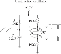

Here is a unijunction transistor (UJT), along with some resistors and a capacitor, that makes up a relaxation oscillator that is capable of generating three different output waveforms. During operation, at one instant in time, C charges through R until the voltage present on the emitter reaches the UJT’s triggering voltage. Once the triggering voltage is exceeded, the E-to-B1 conductivity increases sharply, which allows current to pass from the capacitor-emitter region through the emitter-base 1 region and then to ground. When this occurs, C suddenly loses its charge, and the emitter voltage suddenly falls below the triggering voltage. After that, the cycle repeats itself. The resulting waveforms generated during this process are shown in the figure. The frequency of oscillation is given by
where η is the UJT’s intrinsic standoff ratio, which is typically around 0.5. See Chap. 4 for more details.
Here a simple relaxation oscillator is built from a Schmitt trigger inverter IC and an RC network. (Schmitt triggers are used to transform slowly changing input waveforms into sharply defined, jitter-free output waveforms (see Chap. 12). When power is first applied to the circuit, the voltage across C is zero, and the output of the inverter is high (+5 V). The capacitor starts charging up toward the output voltage via R. When the capacitor voltage reaches the positive-going threshold of the inverter (e.g., 1.7 V), the output of the inverter goes low (∼0 V). With the output low, C discharges toward 0 V. When the capacitor voltage drops below the negative-going threshold voltage of the inverter (e.g., 0.9 V), the output of the inverter goes high. The cycle repeats. The on/off times are determined by the positive- and negative-going threshold voltages and the RC time constant.
The third example is a pair of CMOS inverters that are used to construct a simple squarewave RC relaxation oscillator. The circuit can work with voltages ranging from 4 to 18 V. The frequency of oscillation is given by
The third example is a pair of CMOS inverters that are used to construct a simple squarewave RC relaxation oscillator. The circuit can work with voltages ranging from 4 to 18 V. The frequency of oscillation is given by
R can be adjusted to vary the frequency. I will discuss CMOS inverters in Chap. 12.
FIGURE 10.5
All the relaxation oscillators shown in this section are relatively simple to construct. Now, as it turns out, there is even an easier way to generate basic waveforms. The easy way is to use an IC especially designed for the task. An incredibly popular squarewave-generating chip that can be programmed with resistors and a capacitor is the 555 timer IC.
10.2 The 555 Timer IC
The 555 timer IC is an incredibly useful precision timer that can act as either a timer or an oscillator. In timer mode—better known as monostable mode—the 555 simply acts as a “one-shot” timer; when a trigger voltage is applied to its trigger lead, the chip’s output goes from low to high for a duration set by an external RC circuit. In oscillator mode—better know as astable mode—the 555 acts as a rectangular-wave generator whose output waveform (low duration, high duration, frequency, etc.) can be adjusted by means of two external RC charge/discharge circuits.
The 555 timer IC is easy to use (requires few components and calculations) and inexpensive and can be used in an amazing number of applications. For example, with the aid of a 555, it is possible to create digital clock waveform generators, LED and lamp flasher circuits, tone-generator circuits (sirens, metronomes, etc.), one-shot timer circuits, bounce-free switches, triangular-waveform generators, frequency dividers, etc.
Figure 10.6 is a simplified block diagram showing what is inside a typical 555 timer IC. The overall circuit configuration shown here (with external components included) represents the astable 555 configuration.

The 555 gets its name from the three 5-kΩ resistors shown in the block diagram. These resistors act as a three-step voltage divider between the supply voltage (VCC) and ground. The top of the lower 5-kΩ resistor (+ input to comparator 2) is set to  VCC, while the top of the middle 5-kΩ resistor (− input to comparator 2) is set to
  VCC. The two comparators output either a high or low voltage based on the analog voltages being compared at their inputs. If one of the comparator’s positive inputs is more positive than its negative input, its output logic level goes high; if the positive input voltage is less than the negative input voltage, the output logic level goes low. The outputs of the comparators are sent to the inputs of an SR (set/reset) flip-flop. The flip-flop looks at the R and S inputs and produces either a high or a low based on the voltage states at the inputs (see Chap. 12).
FIGURE 10.6
Pin 1 (ground). IC ground.
Pin 2 (trigger). Input to comparator 2, which is used to set the flip-flop. When the voltage at pin 2 crosses from above to below VCC, the comparator switches to high, setting the flip-flop.
Pin 3 (output). The output of the 555 is driven by an inverting buffer capable of sinking or sourcing around 200 mA. The output voltage levels depend on the output current but are approximately Vout(high) = VCC – 1.5 V and Vout(low) = 0.1 V.
Pin 4 (reset). Active-low reset, which forces  high and pin 3 (output) low.
Pin 5 (control). Used to override the VCC level, if needed, but is usually grounded via a 0.01-μF bypass capacitor (the capacitor helps eliminate VCC supply noise). An external voltage applied here will set a new trigger voltage level.
Pin 6 (threshold). Input to the upper comparator, which is used to reset the flip-flop. When the voltage at pin 6 crosses from below to above VCC, the comparator switches to a high, resetting the flip-flop.
Pin 7 (discharge). Connected to the open collector of the npn transistor. It is used to short pin 7 to ground when is high (pin 3 low). This causes the capacitor to discharge.
Pin 8 (Supply voltage VCC). Typically between 4.5 and 16 V for general-purpose TTL 555 timers. (For CMOS versions, the supply voltage may be as low as 1 V.)
In the astable configuration, when power is first applied to the system, the capacitor is uncharged. This means that 0 V is placed on pin 2, forcing comparator 2 high. This in turn sets the flip-flop so that is high and the 555’s output is low (a result of the inverting buffer). With high, the discharge transistor is turned on, which allows the capacitor to charge toward VCC through R1 and R2. When the capacitor voltage exceeds VCC, comparator 2 goes low, which has no effect on the SR flip-flop. However, when the capacitor voltage exceeds VCC, comparator 1 goes high, resetting the flip-flop and forcing high and the output low. At this point, the discharge transistor turns on and shorts pin 7 to ground, discharging the capacitor through R2. When the capacitor’s voltage drops below VCC, comparator 2’s output jumps back to a high level, setting the flip-flop and making low and the output high. With low, the transistor turns on, allowing the capacitor to start charging again. The cycle repeats over and over again. The net result is a squarewave output pattern whose voltage level is approximately VCC − 1.5 V and whose on/off periods are determined by the C, R1 and R2.
10.2.2 Basic Astable Operation
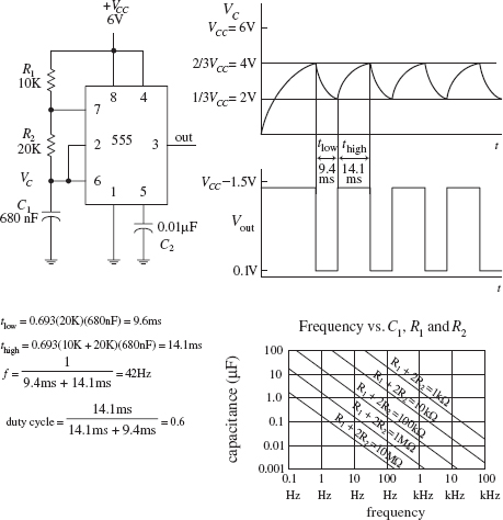
When a 555 is set up in astable mode, it has no stable states; the output jumps back and forth. The time duration Vout remains low (around 0.1 V) is set by the R1C1 time constant and the VCC and VCC levels; the time duration Vout stays high (around VCC −1.5 V) is determined by the (R1 + R2) C1 time constant and the two voltage levels (see graphs). After doing some basic calculations, the following two practical expressions arise:
tlow = 0.693R2C1
thigh = 0.693(R1 + R2)C1
thigh = 0.693(R1 + R2)C1
The duty cycle (the fraction of the time the output is high) is given by
The frequency of the output waveform is
For reliable operation, the resistors should be between approximately 10 kΩ and 14 MΩ, and the timing capacitor should be from around 100 pF to 1000 μF. The graph will give you a general idea of how the frequency responds to the component values.
FIGURE 10.7

Now there is a slight problem with the last circuit—you cannot get a duty cycle that is below 0.5 (or 50 percent). In other words, you cannot make thigh shorter than tlow. For this to occur, the R1C1 network (used to generate tlow) would have to be larger the (R1 + R2)C1 network (used to generate thigh). Simple arithmetic tells us that this is impossible; (R1 + R2)C1 is always greater than R1C1. How do you remedy this situation? You attach a diode across R2, as shown in the figure. With the diode in place, as the capacitor is charging (generating thigh), the preceding time constant (R1 + R2)C1 is reduced to R1C1 because the charging current is diverted around R2 through the diode. With the diode in place, the high and low times become

FIGURE 10.8
Figure 10.9 shows a 555 hooked up in the monostable configuration (one-shot mode). Unlike the astable mode, the monostable mode has only one stable state. This means that for the output to switch states, an externally applied signal is needed.
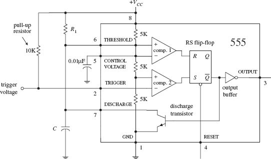
FIGURE 10.9
In the monostable configuration, initially (before a trigger pulse is applied) the 555’s output is low, while the discharge transistor is on, shorting pin 7 to ground and keeping C discharged. Also, pin 2 is normally held high by the 10-k pull-up resistor. Now, when a negative-going trigger pulse (less than VCC) is applied to pin 2, comparator 2 is forced high, which sets the flip-flop’s to low, making the output high (due to the inverting buffer), while turning off the discharge transistor. This allows C to charge up via R1 from 0 V toward VCC. However, when the voltage across the capacitor reaches VCC, comparator 1’s output goes high, resetting the flip-flop and making the output low, while turning on the discharge transistor, allowing the capacitor to quickly discharge toward 0 V. The output will be held in this stable state (low) until another trigger is applied.

The monostable circuit only has one stable state. That is, the output rests at 0 V (in reality, more like 0.1 V) until a negative-going trigger pulse is applied to the trigger lead—pin 2. (The negative-going pulse can be implemented by momentarily grounding pin 2, say, by using a pushbutton switch attached from pin 2 to ground.) After the trigger pulse is applied, the output will go high (around VCC − 1.5 V) for the duration set by the R1C1 network. Without going through the derivations, the width of the high output pulse is
twidth = 1.10R1C1
For reliable operation, the timing resistor R1 should be between around 10 kΩ and 14 MΩ, and the timing capacitor should be from around 100 pF to 1000 μF.
FIGURE 10.10
10.2.5 Some Important Notes About 555 Timers
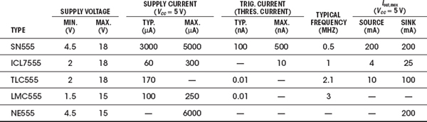
555 ICs are available in both bipolar and CMOS types. Bipolar 555s, like the ones you used in the preceding examples, use bipolar transistors inside, while CMOS 555s use MOSFET transistors instead. These two types of 555s also differ in terms of maximum output current, minimum supply voltage/current, minimum triggering current, and maximum switching speed. With the exception of maximum output current, the CMOS 555 surpasses the bipolar 555 in all regards. A CMOS 555 IC can be distinguished from a bipolar 555 by noting whether the part number contains a C somewhere within it (e.g., ICL7555, TLC555, LMC555, etc.). (Note that there are hybrid versions of the 555 that incorporate the best features of both the bipolar and CMOS technologies.) Table 10.1 shows specifications for a few 555 devices.
TABLE 10.1 Sample Specifications for Some 555 Devices
If you need more than one 555 timer per IC, check out the 556 (dual version) and 558 (quad version). The 556 contains two functionally independent 555 timers that share a common supply lead, while the 558 contains four slightly simplified 555 timers. In the 558, not all functions are brought out to the pins, and in fact, this device is intended to be used in monostable mode—although it can be tricked into astable mode with a few alterations (see manufacturer’s literature for more information).

FIGURE 10.11
PRACTICAL TIP
To avoid problems associated with false triggering, connect the 555’s pin 5 to ground through a 0.01-μF capacitor (we applied this trick already in this section). Also, if the power supply lead becomes long or the timer does not seem to function for some unknown reason, try attaching a 0.1-μF or larger capacitor between pins 8 and 1.
10.2.6 Simple 555 Applications
Relay Driver (Delay Timer)

The monostable circuit shown here acts as a delay timer that is used to actuate a relay for a given duration. With the pushbutton switch open, the output is low (around 0.1 V), and the relay is at rest. However, when the switch is momentarily closed, the 555 begins its timing cycle; the output goes high (in this case ∼10.5 V) for a duration equal to
tdelay = 1.10R1C1
The relay will be actuated for the same time duration. The diodes help prevent damaging current surges—generated when the relay switches states—from damaging the 555 IC, as well as the relay’s switch contacts.
FIGURE 10.12
LED and Lamp Flasher and Metronome

All these circuits are oscillator circuits (astable multivibrators). In the LED flasher circuit, a transistor is used to amplify the 555’s output in order to provide sufficient current to drive the LED, while RS is used to prevent excessive current from damaging the LED. In the lamp-flasher circuit, a MOSFET amplifier is used to control current flow through the lamp. A power MOSFET may be needed if the lamp draws a considerable amount of current. The metronome circuit produces a series of “clicks” at a rate determined by R2. To control the volume of the clicks, R4 can be adjusted.
FIGURE 10.13
10.3 Voltage-Controlled Oscillators
Besides the 555 timer IC, there are a number of other voltage-controlled oscillators (VCOs) on the market—some of which provide more than just a squarewave output. For example, the NE566 function generator is a very stable, easy-to-use triangular-wave and squarewave generator. In the 566 circuit below, R1 and C1 set the center frequency, while a control voltage at pin 5 varies the frequency; the control voltage is applied by means of a voltage-divider network (R2, R3, R4). The output frequency of the 566 can be determined by using the formula shown in Fig. 10.14.

FIGURE 10.14
Other VCOs, such as the 8038 and the XR2206, can create a trio of output waveforms, including a sine wave (approximation of one, at any rate), a square wave, and triangular wave. Some VCOs are designed specifically for digital waveform generation and may use an external crystal in place of a capacitor for improved stability. To get a feel for what kinds of VCOs are out there, check the electronics catalogs.
10.4 Wien-Bridge and Twin-T Oscillators
A popular RC-type circuit used to generate low-distortion sinusoidal waves at low to moderate frequencies is the Wien-bridge oscillator. Unlike the oscillator circuits discussed already in this chapter, this oscillator uses a different kind of mechanism to provide oscillation, namely, a frequency-selective filter network.

The heart of the Wien-bridge oscillator is its frequency-selective feedback network. The op amp’s output is fed back to the inputs in phase. Part of the feedback is positive (makes its way through the frequency-selective RC branch to the noninverting terminal), while the other part is negative (is sent through the resistor branch to the inverting input of the op amp). At a particular frequency f0 = 1/(2πRC), the inverting input voltage (V4) and the noninverting input voltage (V2) will be equal and in phase—the positive feedback will cancel the negative feedback, and the circuit will oscillate. At any other frequency, V2 will be too small to cancel V4, and the circuit will not oscillate. In this circuit, the gain must be set to +3. The resistors must satisfy the condition R3/R4 = 2 (which gives a noninverting gain of 3). Anything less than this value will cause oscillations to cease; anything more will cause the output to saturate. With the component values listed in the figure, this oscillator can cover a frequency range of 1 to 5 kHz. The frequency can be adjusted by means of a two-ganged variable-capacitor unit.
The second circuit shown in the figure is a slight variation of the first. Unlike the first circuit, the positive feedback must be greater than the negative feedback to sustain oscillations. The potentiometer is used to adjust the amount of negative feedback, while the RC branch controls the amount of positive feedback based on the operating frequency. Now, since the positive feedback is larger than the negative feedback, you have to contend with the “saturation problem,” as encountered in the last example. To prevent saturation, two zener diodes placed face to face (or back to back) are connected across the upper 22-kΩ resistor. When the output voltage rises above the zener’s breakdown voltage, one or the other zener diode conducts, depending on the polarity of the feedback. The conducting zener diode shunts the 22-kΩ resistor, causing the resistance of the negative feedback circuit to decrease. More negative feedback is applied to the op amp, and the output voltage is controlled to a certain degree.
The second circuit shown in the figure is a slight variation of the first. Unlike the first circuit, the positive feedback must be greater than the negative feedback to sustain oscillations. The potentiometer is used to adjust the amount of negative feedback, while the RC branch controls the amount of positive feedback based on the operating frequency. Now, since the positive feedback is larger than the negative feedback, you have to contend with the “saturation problem,” as encountered in the last example. To prevent saturation, two zener diodes placed face to face (or back to back) are connected across the upper 22-kΩ resistor. When the output voltage rises above the zener’s breakdown voltage, one or the other zener diode conducts, depending on the polarity of the feedback. The conducting zener diode shunts the 22-kΩ resistor, causing the resistance of the negative feedback circuit to decrease. More negative feedback is applied to the op amp, and the output voltage is controlled to a certain degree.
FIGURE 10.15
10.5 LC Oscillators (Sinusoidal Oscillators)
When it comes to generating high-frequency sinusoidal waves, commonly used in radiofrequency applications, the most common approach is to use an LC oscillator. The RC oscillators discussed so far have difficulty handling high frequencies, mainly because it is difficult to control the phase shifts of feedback signals sent to the amplifier input and because, at high frequencies, the capacitor and resistor values often become impractical to work with. LC oscillators, on the other hand, can use small inductances in conjunction with capacitance to create feedback oscillators that can reach frequencies up to around 500 MHz. However, it is important to note that at low frequencies (e.g., audio range), LC oscillators become highly unwieldy.
LC oscillators basically consist of an amplifier that incorporates positive feedback through a frequency-selective LC circuit (or tank). The LC tank acts to eliminate from the amplifier’s input any frequencies significantly different from its natural resonant frequency. The positive feedback, along with the tank’s resonant behavior, acts to promote sustained oscillation within the overall circuit. If this is a bit confusing, envision shock exciting a parallel LC tank circuit. This action will set the tank circuit into sinusoidal oscillation at the LC’s resonant frequency—the capacitor and inductor will “toss” the charge back and forth. However, these oscillations will die out naturally due to internal resistance and loading. To sustain the oscillation, the amplifier is used. The amplifier acts to supply additional energy to the tank circuit at just the right moment to sustain oscillations. Here is a simple example to illustrate the point.

Here, an op amp incorporates positive feedback that is altered by an LC resonant filter or tank circuit. The tank eliminates from the noninverting input of the op amp any frequencies significantly different from the tank’s natural resonant frequency:
(Recall from Chap. 2 that a parallel LC resonant circuit’s impedance becomes large at the resonant frequency but falls off on either side, allowing the feedback signal to be filtered out to ground.) If a sinusoidal voltage set at the resonant frequency is present at V1, the amplifier is alternately driven to saturation in the positive and negative directions, resulting in a square wave at the output V2. This square wave has a strong fundamental Fourier component at the resonant frequency, part of which is fed back to the noninverting input through the resistor to keep oscillations from dying out. If the initially applied sinusoidal voltage at V1 is removed, oscillations will continue, and the voltage at V1 will be sinusoidal. Now in practice (considering real-life components and not theoretical models), it is not necessary to apply a sine wave to V1 to get things going (this is a fundamentally important point to note). Instead, due to imperfections in the amplifier, the oscillator will self-start. Why? With real amplifiers, there is always some inherent noise present at the output even when the inputs of the amplifier are grounded (see Chap. 8). This noise has a Fourier component at the resonant frequency, and because of the positive feedback, it rapidly grows in amplitude (perhaps in just a few cycles) until the output amplitude saturates.
FIGURE 10.16
Now, in practice, LC oscillators usually do not incorporate op amps into their designs. At very high frequencies (e.g., RF range), op amps tend to become unreliable due to slew-rate and bandwidth limitations. When frequencies above around 100 kHz are needed, it is essential to use another kind of amplifier arrangement. For high-frequency applications, what is typically used is a transistor amplifier (e.g., bipolar or FET type). The switching speeds for transistors can be incredibly high—a 2000-MHz ceiling is not uncommon for special RF transistors. However, when using a transistor amplifier within an oscillator, there may be a slight problem to contend with—one that you did not have to deal with when you used the op amp. The problem stems from the fact that transistor-like amplifiers often take their outputs at a location where the output happens to be 180° out of phase with its input (see Chap. 4). However, for the feedback to sustain oscillations, the output must be in phase with the input. In certain LC oscillators this must be remedied by incorporating a special phase-shifting network between the output and input of the amplifier. Let’s take a look at a few popular LC oscillator circuits.

A Hartley oscillator uses an inductive voltage divider to determine the feedback ratio. The Hartley oscillator can take on a number of forms (FET, bipolar, etc.)—a JFET version is shown here. This oscillator achieves a 180° phase shift needed for positive feedback by means of a tapped inductor in the tank circuit. The phase voltage at the two ends of the inductor differ by 180° with respect to the ground tap. Feedback via L2 is coupled through C1 to the base of the transistor amplifier. (The tapped inductor is basically an autotransformer, where L1 is the primary and L2 is the secondary.) The frequency of the Hartley is determined by the tank’s resonant frequency:
This frequency can be adjusted by varying CT. RG acts as a gate-biasing resistor to set the gate voltage. RS is the source resistor. CS is used to improve amplifier stability, while C1 and C2 act as a dc-blocking capacitor that provides low impedance at the oscillator’s operating frequency while preventing the transistor’s dc operating point from being disturbed. The radiofrequency choke (RFC) aids in providing the amplifier with a steady dc supply while eliminating unwanted ac disturbances.
The second circuit is another form of the Hartley oscillator that uses a bipolar transistor instead of a JFET as the amplifier element. The frequency of operation is again determined by the resonant frequency of the LC tank. Notice that in this circuit the load is coupled to the oscillator via a transformer’s secondary.
The second circuit is another form of the Hartley oscillator that uses a bipolar transistor instead of a JFET as the amplifier element. The frequency of operation is again determined by the resonant frequency of the LC tank. Notice that in this circuit the load is coupled to the oscillator via a transformer’s secondary.
FIGURE 10.17

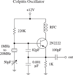
The Colpitts oscillator is adaptable to a wide range of frequencies and can have better stability than the Hartley. Unlike the Hartley, feedback is obtained by means of a tap between two capacitors connected in series. The 180° phase shift required for sustained oscillation is achieved by using the fact that the two capacitors are in series; the ac circulating current in the LC circuit (see Chap. 2) produces voltage drops across each capacitor that are of opposite signs—relative to ground—at any instant in time. As the tank circuit oscillates, its two ends are at equal and opposite voltages, and this voltage is divided across the two capacitors. The signal voltage across C4 is then connected to the transistor’s base via coupling capacitor C1, which is part of the signal from the collector. The collector signal is applied across C3 as a feedback signal whose energy is coupled into the tank circuit to compensate for losses. The operating frequency of the oscillator is determined by the resonant frequency of the LC tank:
where Ceff is the series capacitance of C3 and C4:
C1 and C2 are dc-blocking capacitors, while R1 and R2 act to set the bias level of the transistor. The RFC choke is used to supply steady dc to the amplifier. This circuit’s tank can be exchanged for one of the two adjustable tank networks. One tank uses permeability tuning (variable inductor), while the other uses a tuning capacitor placed across the inductor to vary the resonant frequency of the tank.
FIGURE 10.18
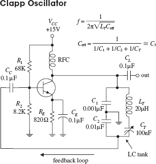
The Clapp oscillator has exceptional frequency stability. It is a simple variation of the Colpitts oscillator. The total tank capacitance is the series combination of C1 and C2. The effective inductance L of the tank is varied by changing the net reactance by adding and subtracting capacitive reactance via CT from inductive reactance of LT. Usually C1 and C2 are much larger than CT, while LT and CT are series resonant at the desired frequency of operation. C1 and C2 determine the feedback ratio, and they are so large compared with CT that adjusting CT has almost no effect on feedback. The Clapp oscillator achieves its reputation for stability since stray capacitances are swamped out by C1 and C2, meaning that the frequency is almost entirely determined by LT and CT. The frequency of operation is determined by
where Ceff is
FIGURE 10.19
10.6 Crystal Oscillators
When stability and accuracy become critical in oscillator design—which is often the case in high-quality radio and microprocessor applications—one of the best approaches is to use a crystal oscillator. The stability of a crystal oscillator (from around 0.01 to 0.001 percent) is much greater than that of an RC oscillator (around 0.1 percent) or an LC oscillator (around 0.01 percent at best).
When a quartz crystal is cut in a specific manner and placed between two conductive plates that act as leads, the resulting two-lead device resembles an RLC tuned resonant tank. When the crystal is shock-excited by either a physical compression or an applied voltage, it will be set into mechanical vibration at a specific frequency and will continue to vibrate for some time, while at the same time generating an ac voltage between its plates. This behavior, better know as the piezoelectric effect, is similar to the damped electron oscillation of a shock-excited LC circuit. However, unlike an LC circuit, the oscillation of the crystal after the initial shock excitation will last longer—a result of the crystal’s naturally high Q value. For a high-quality crystal, a Q of 100,000 is not uncommon. LC circuits typically have a Q of around a few hundred.
The RLC circuit shown in Fig. 10.20 is used as an equivalent circuit for a crystal. The lower branch of the equivalent circuit, consisting of R1, C1, and L1 in series, is called the motional arm. The motional arm represents the series mechanical resonance of the crystal. The upper branch containing C0 accounts for the stray capacitance in the crystal holder and leads. The motional inductance L1 is usually many henries in size, while the motional capacitance C1 is very small (<<1 pF). The ratio of L1 to C1 for a crystal is much higher than could be achieved with real inductors and capacitors. Both the internal resistance of the crystal R1 and the value of C0 are both fairly small. (For a 1-MHz crystal, the typical components values within the equivalent circuit would be L1 = 3.5 H, C1 = 0.007 pF, R1 = 340 Ω, C0 = 3 pF. For a 10-MHz fundamental crystal, the typical values would be L1 = 9.8 mH, C1 = 0.026 pF, R1 = 7 Ω, C0 = 6.3 pF.)

FIGURE 10.20
In terms of operation, a crystal can be driven at series resonance or parallel resonance. In series resonance, when the crystal is driven at a particular frequency, called the series resonant frequency fs, the crystal resembles a series-tuned resonance LC circuit; the impedance across it goes to a minimum—only R1 remains. In parallel resonance, when the crystal is driven at what is called the parallel resonant frequency fp, the crystal resembles a parallel-tuned LC tank; the impedance across it peaks to a high value (see the graphs in Fig. 10.20).
Quartz crystals come in series-mode and parallel-mode forms and may either be specified as a fundamental-type or an overtone-type crystal. Fundamental-type crystals are designed for operation at the crystal’s fundamental frequency, while overtone-type crystals are designed for operation at one of the crystal’s overtone frequencies. (The fundamental frequency of a crystal is accompanied by harmonics or overtone modes, which are odd multiples of the fundamental frequency. For example, a crystal with a 15-MHz fundamental also will have a 45-MHz third overtone, a 75-MHz fifth overtone, a 135-MHz ninth overtone, etc. Figure 10.21 below shows an equivalent RLC circuit for a crystal, along with a response curve, both of which take into account the overtones.) Fundamental-type crystals are available from around 10 kHz to 30 MHz, while overtone-type crystals are available up to a few hundred megahertz. Common frequencies available are 100 kHz and 1.0, 2.0, 4, 5, 8, and 10 MHz.
Designing crystal oscillator circuits is similar to designing LC oscillator circuits, except that now you replace the LC tank with a crystal. The crystal will supply positive feedback and gain at its series or parallel resonant frequency, hence leading to sustained oscillations. Here are a few basic crystal oscillator circuits to get you started.
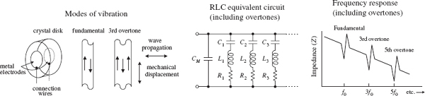
FIGURE 10.21

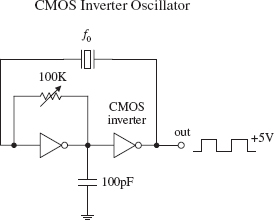
The simple op amp circuit shown here resembles the LC oscillator circuit in Fig. 10.16, except that it uses the series resonance of the crystal instead of the parallel resonance of an LC circuit to provide positive feedback at the desired frequency. Other crystal oscillators, such as the Pierce oscillator, Colpitts oscillator, and a CMOS inverter oscillator, shown below, also incorporate a crystal as a frequency-determining component. The Pierce oscillator, which uses a JFET amplifier stage, employs a crystal as a series-resonant feedback element; maximum positive feedback from drain to gate occurs only at the crystal’s series-resonant frequency. The Colpitts circuit, unlike the Pierce circuit, uses a crystal in the parallel feedback arrangement; maximum base-emitter voltage signal occurs at the crystal’s parallel-resonant frequency. The CMOS circuit uses a pair of CMOS inverters along with a crystal that acts as a series-resonant feedback element; maximum positive feedback occurs at the crystal’s series resonant frequency.
FIGURE 10.22
There are a number of ICs available that can make designing crystal oscillators a breeze. Some of these ICs, such as the 74S124 TTL VCO (squarewave generator), can be programmed by an external crystal to output a waveform whose frequency is determined by the crystal’s resonant frequency. The MC12060 VCO, unlike the 74S124, outputs a pair of sine waves. Check the catalogs to see what other types of oscillator ICs are available.
Now there are also crystal oscillator modules that contain everything (crystal and all) in one single package. These modules resemble a metal-like DIP package, and they are available in many of the standard frequencies (e.g., 1, 2, 4, 5, 6, 10, 16, 24, 25, 50, and 64 MHz, etc.). Again, check out the electronics catalogs to see what is available.
10.7 Microcontroller Oscillators
In Chap. 13, we will also see how a microcontroller can be used to generate a waveform using a digital-to-analog convertor. The basic technique is to store the waveform in memory and then play it through the digital-to-analog converter.
In the case where just a squarewave is required, a simple 8-pin microcontroller with a built-in clock can be an effective alternative to a 555 timer, requiring fewer external components.
..................Content has been hidden....................
You can't read the all page of ebook, please click here login for view all page.