
5
Communication Techniques
In Chapters 1 to 4, after an introduction to the evolution of satellites and satellite technology, the principles of satellite launch, in-orbit operations and its functioning have been covered in detail followed by a detailed account of satellite hardware including various subsystems that combine to make the spacecraft. In Chapters 5, 6 and 7, the focus shifts to topics that relate mainly to communication satellites, which account for more than 80 % of satellites present in space, more than 80 % of applications configured around satellites and more than 80 % of the budget spent on development of satellite technology as a whole. The topics covered in the first of the three chapters, that is the present chapter, mainly include modulation and demodulation techniques (both analogue and digital) and multiplexing techniques, followed by multiple access techniques in the next chapter. Chapter 7 focuses on satellite link design related aspects. All three chapters are amply illustrated with a large number of solved problems.
5.1 Types of Information Signals
When it comes to transmitting information over an RF communication link, be it a terrestrial link or a satellite link, it is essentially voice or data or video. A communication link therefore handles three types of signals, namely voice signals like those generated in telephony, radio broadcast and the audio portion of a television broadcast; data signals produced in computer-to-computer communications; and video signals like those generated in a television broadcast or video conferencing. Each of these signals is referred to as a base band signal. The base band signal is subjected to some kind of processing, known as base band processing, to convert the signal to a form suitable for transmission. Band limiting of speech signals to 3000 Hz in telephony and use of coding techniques in the case of digital signal transmission are examples of base band processing. The transformed base band signal then modulates a high frequency carrier so that it is suitable for propagation over the chosen transmission link. The demodulator on the receiver end recovers the base band signal from the received modulated signal. Modulation, demodulation and other relevant techniques will be discussed in the following pages of this chapter. However, before that, a brief outline on the three types of information signals mentioned above follows.
5.1.1 Voice Signals
Though the human ear is sensitive to a frequency range of 20 to 20 kHz, the frequency range of a speech signal is less than this. For the purpose of telephony, the speech signal is band limited to an upper limit of 3400 Hz during transmission. The quality of a received analogue voice signal has been specified by CCITT (Comité Consultatif International de Télégraphique et Téléphonique) to give a worst case base band signal-to-noise ratio of 50 dB. Here the signal is considered to be a standard test tone and the maximum allowable base band signal noise power is 10 nW. Apart from the signal bandwidth and signal-to-noise ratio, another important parameter that characterizes the voice signal is its dynamic range. A speech or voice signal is characterized to have a large dynamic range of 50 dB.
In the case of digital transmission, the quality of the recovered speech signal depends upon the number of bits transmitted per second and the bit error rate (BER). The BER required to give a good quality speech is considered to be 10−4; i.e. 1 bit error in 10 kB though a BER of 10−5 or better is common.
5.1.2 Data Signals
Data signals refer to a digitized version of a large variety of information services, including voice telephony and a video and computer generated information exchange. It is indeed the most commonly used vehicle for information transfer due to its ability to combine on a single transmission support the data generated by a number of individual services, which is of great significance when it comes to transmitting multimedia traffic integrating voice, video and application data.
Again it is the system bandwidth that determines how fast the data can be sent in a given period of time, expressed in bits per second (bps). Obviously, the bigger the size of the file to be transferred in a given time, faster is the required data transfer rate or larger is the required bandwidth. Transmission of a video signal requires a much larger data transmission rate (or bandwidth) than that required by transmission of a graphics file. A graphics file requires a much larger data transfer rate than that required by a text file. The desired data rate may vary from a few tens of kbps to hundreds of Mbps for various information services. However, data compression techniques allow transmission of signals at a rate much lower than that theoretically needed to do so.
5.1.3 Video Signals
The frequency range or bandwidth of a video signal produced as a result of television quality picture information depends upon the size of the smallest picture information, referred to as a pixel. The larger the number of pixels, the higher is the signal bandwidth. As an example, in the 625 line, 50 Hz television standard where each picture frame having 625 lines is split into two fields of 312 1 /2 lines and the video signal is produced as a result of scanning 50 fields per second in an interlaced scanning mode. Assuming a worst case picture pattern where pixels alternate from black to white to generate one cycle of video output, the highest video frequency is given by:

where
- a = aspect ratio = 4/3
- N = number of lines per frame
- th = time period for scanning one horizontal line
For the 625 line, 50 Hz system, it turns out to be 6.5 MHz. The above calculation does not, however, take into account the lines suppressed during line and frame synchronization. For actual picture transmission, the chosen bandwidth is 5 MHz for the 625 line, 50 Hz system and 4.2 MHz for the 525 line, 60 Hz system. The reduced bandwidth does not seem to have any detrimental effect on picture quality.
5.2 Amplitude Modulation
Amplitude modulation (AM) is not used as such in any of the satellite link systems. A brief overview of it is given as it may be used to modulate individual voice channels, which then can be multiplexed using frequency division multiplexing before the composite signal finally modulates another carrier.
In amplitude modulation, the instantaneous amplitude of the modulated signal varies directly as the instantaneous amplitude of the modulating signal. The frequency of the modulated signal remains the same as the carrier signal frequency. Figure 5.1 shows the modulating signal, the carrier signal and the modulated signal in the case of a single tone modulating signal.
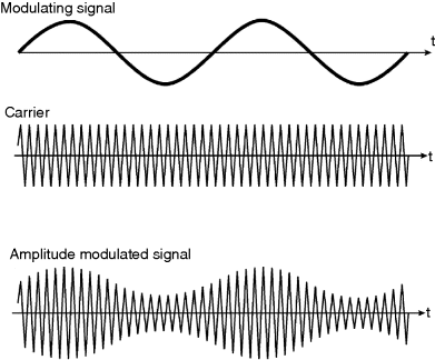
Figure 5.1 Amplitude modulation
If the modulating signal and the carrier signal are expressed respectively by ![]() and
and ![]() , then the amplitude modulated signal
, then the amplitude modulated signal ![]() can be expressed mathematically by
can be expressed mathematically by
where m = modulation index = Vm/Vc. When more than one sinusoidal or cosinosoidal signals with different amplitudes modulate a carrier, the overall modulation index in that case is given by
where m1, m2 and m3 are modulation indices corresponding to the individual signals. The percentage of modulation or depth of modulation is given by (m × 100) and for a depth of modulation equal to 100 %, m = 1 or Vm = Vc.
5.2.1 Frequency Spectrum of the AM Signal
Expanding the expression for the modulated signal given above, we get
The frequency spectrum of an amplitude modulated signal in the case of a single frequency modulating signal thus contains three frequency components, namely the carrier frequency component (ωc), the sum frequency component (ωc + ωm) and the difference frequency component (ωc–ωm). The sum component represents the upper side band and the difference component the lower side band. Figure 5.2 shows the frequency spectrum.
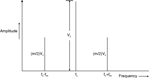
Figure 5.2 Frequency spectrum of the AM signal for a single frequency modulating signal
It may be mentioned here that in actual practice, the modulating signal is not a single frequency tone. In fact, it is a complex signal. This complex signal can always be represented mathematically in terms of sinusoidal and cosinosoidal components. Thus if a given modulating signal is equivalently represented as a sum of, say, three components (ωm1, ωm2 and ωm3), then the frequency spectrum of the AM signal, when such a complex signal modulates a carrier, contains the frequency components ωc, ωc + ωm1, ωc − ωm1, ωc + ωm2, ωc − ωm2, ωc + ωm3 and ωc − ωm3.
5.2.2 Power in the AM Signal
The total power Pt in an AM signal is related to the unmodulated carrier power Pc by
This can be interpreted as
where Pcm2/4 is the power in either of the two side bands, i.e. the upper and lower side bands. For 100 % depth of modulation for which m = 1, the total power in an AM signal is 3Pc/2 and the power in each of the two side bands is Pc/4 with the total side band power equal to Pc/2. These expressions indicate that even for 100 % depth of modulation, the power contained in the side bands, which contain actual information to be transmitted, is only one-third of the total power in the AM signal.
The power content of different parts of the AM signal can also be expressed in terms of the peak amplitude of an unmodulated carrier signal (Vc) as
where, R is the resistance in which the power is dissipated (e.g. antenna resistance).
5.2.3 Noise in the AM Signal
The noise performance when an AM signal is contaminated with noise will now be examined. S, C and N are assumed to be the signal, carrier and noise power levels respectively. It is also assumed that the receiver has a bandwidth B, which in the case of a conventional double side band system equals 2fm, where fm is the highest modulating frequency. If Nb is the noise power at the output of the demodulator, then
where A is the scaling factor for the demodulator. Signal power in each of the side band frequencies at maximum is equal to one-quarter of the carrier power, as explained in the earlier paragraphs; i.e.
and
where
- SL = signal power in the lower side band frequency before demodulation
- SU = signal power in the upper side band frequency before demodulation
- SbL = signal power in the lower side band frequency after demodulation
- SbU = signal power in the upper side band frequency after demodulation
Since both lower and upper side band frequencies are identical before and after demodulation, they will add coherently in the demodulator to produce a total base band power Sb given by
Combining the expressions for Sb and Nb gives the following relationship between Sb/Nb and C/N:
where N = NoB, with No being the noise power spectral density in W/Hz and B being the receiver bandwidth.
This relationship is, however, valid only for a modulation index of unity. The generalized expression for the modulation index of m will be
So far, a single frequency modulating signal has been discussed. In the case where the modulating signal is a band of frequencies, the frequency spectrum of the AM signal would comprise of lower and upper frequency bands such as the one shown in Figure 5.3. Incidentally, the spectrum shown represents a case where the modulating signal is the base band telephony signal ranging from 300 Hz to 3400 Hz.

Figure 5.3 Frequency spectrum of the AM signal for a multifrequency modulating signal
5.2.4 Different Forms of Amplitude Modulation
In the preceding paragraphs it was seen that the process of amplitude modulation produces two side bands, each of which contains the complete base band signal information. Also, the carrier contains no base band signal information. Therefore, if one of the side bands was suppressed and only one side band transmitted, it would make no difference to the information content of the modulated signal. In addition, it would have the advantage of requiring only one half of the bandwidth as compared to the conventional double side band signal. If the carrier was also suppressed before transmission, it would lead to a significant saving in the required transmitted power for a given power in the information carrying signal. That is why, the single side band suppressed carrier mode of amplitude modulation is very popular. In the following paragraphs, some of the practical forms of amplitude modulation systems will be briefly outlined.
5.2.4.1 A3E System
This is the standard AM system used for broadcasting. It uses a double side band with a full carrier. The standard AM signal can be generated by adding a large carrier signal to the double side band suppressed carrier (DSBSC) or simply the double side band (DSB) signal. The DSBSC signal in turn can be generated by multiplying the modulating signal m(t) and the carrier (cos ωct). Figure 5.4 shows the arrangement of generating the DSBSC signal.

Figure 5.4 Generation of the DSBSC signal
Demodulation of the standard AM signal is very simple and is implemented by using what is known as the envelope detection technique. In a standard AM signal, when the amplitude of the unmodulated carrier signal is very large, the amplitude of the modulated signal is proportional to the modulating signal. Demodulation in this case simply reduces to detection of the envelope of the modulated signal regardless of the exact frequency or phase of the carrier. Figure 5.5 shows the envelope detector circuit used for demodulating the standard AM signal. The capacitor (C) filters out the high frequency carrier variations.
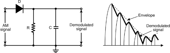
Figure 5.5 Envelope detector for demodulating standard AM signal
Demodulation of the DSBSC signal is carried out by multiplying the modulated signal by a locally generated carrier signal and then passing the product signal through a lowpass filter (LPF), as shown in Figure 5.6.

Figure 5.6 Demodulation of the DSBSC signal
5.2.4.2 H3E System
This is the single side band full carrier system (SSBFC). H3E transmission could be used with A3E receivers with distortion not exceeding 5 %. One method to generate a single side band (SSB) signal is first to generate a DSB signal first and then suppress one of the side bands by the process of filtering using a bandpass filter (BPF). This method, known as the frequency discrimination method, is illustrated in Figure 5.7. In practice, this approach poses some difficulty because the filter needs to have sharp cut-off characteristics.
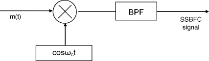
Figure 5.7 Frequency discrimination method for generating the SSBFC signal
Another method for generating an SSB signal is the phase shift method. Figure 5.8 shows the basic block schematic arrangement. The blocks labelled −π/2 are phase shifters that add a lagging phase shift of π/2 to every frequency component of the signal applied at the input to the block. The output block can either be an adder or a subtractor. If m(t) is the modulating signal and m′ (t) is the modulating signal delayed in phase by π/2, then the SSB signal produced at the output can be represented by
The output with the plus sign is produced when the output block is an adder and with the minus sign when the output block is a subtractor.

Figure 5.8 Phase shift method for generating the SSBFC signal
The difference signal represents the upper side band SSB signal while the sum represents the lower side band SSB signal. For instance, if m(t) is taken as cos ωmt, then m ' (t) would be sin ωmt. The SSB signal in the case of the minus sign would then be
and in the case of the plus sign, it would be
5.2.4.3 R3E System
This is the single side band reduced carrier (SSBRC) system, also called the pilot carrier system. Re-insertion of the carrier with much reduced amplitude before transmission is aimed at facilitating receiver tuning and demodulation. This reduced carrier amplitude is 16 dB or 26 dB below the value it would have, had it not been suppressed in the first place. This attenuated carrier signal, while retaining the advantage of saving in power, provides a reference signal to help demodulation in the receiver.
5.2.4.4 J3E System
This is the single side band suppressed carrier (SSBSC) system and is usually referred to as the SSB, in which the carrier is suppressed by at least 45 dB in the transmitter. It was not popular initially due to the requirement for high receiver stability. However, with the advent of synthesizer driven receivers, it has now become the standard form of radio communication.
Generation of SSB signals was briefly described in earlier paragraphs. Suppression of the carrier in an AM signal is achieved in the building block known as the balanced modulator (BM). Figure 5.9 shows the typical circuit implemented using field effect transistors (FETs). The modulating signal is applied in push–pull to a pair of identical FETs as shown and, as a result, the modulating signals appearing at the gates of the two FETs are 180° out of phase. The carrier signal, as is evident from the circuit, is applied to the two gates in phase. The modulated output currents of the two FETs produced as a result of their respective gate signals are combined in the centre tapped primary of the output transformer. If the two halves of the circuit are perfectly symmetrical, it can be proved with the help of simple mathematics that the carrier signal frequency will be completely cancelled in the modulated output and the output would contain only the modulating frequency, the sum frequency and the difference frequency components. The modulating frequency component can be removed from the output by tuning the output transformer.
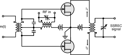
Figure 5.9 Balanced modulator
Demodulation of SSBSC signals can be implemented by using a coherent detector scheme, as outlined in case of demodulation of the DSBSC signal in earlier paragraphs. Figure 5.10 shows the arrangement.
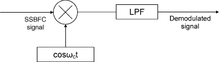
Figure 5.10 Coherent detector for demodulation of the SSBSC signal
5.2.4.5 B8E System
This system uses two independent side bands with the carrier either attenuated or suppressed. This form of amplitude modulation is also known as independent side band (ISB) transmission and is usually employed for point-to-point radio telephony.
5.2.4.6 C3F System
Vestigial side band (VSB) transmission is the other name for this system. It is used for transmission of video signals in commercial television broadcasting. It is a compromise between SSB and DSB modulation systems in which a vestige or part of the unwanted side band is also transmitted, usually with a full carrier along with the other side band. The typical bandwidth required to transmit a VSB signal is about 1.25 times that of an SSB signal. VSB transmission is used in commercial television broadcasting to conserve bandwidth. Figure 5.11 shows the spectrum of transmitted signals in the case of NTSC (National Television System Committee) TV standards followed in the United States, Canada and Japan Figure 5.11 (a) and PAL (Phase Alternation Line) TV standards followed in Europe, Australia and elsewhere [Figure 5.11 (b)]. As can be seen from the two figures, if the channel width is from, say, A to B MHz, the picture carrier is at (A + 1.25) MHz and the sound carrier is at (B − 0.25) MHz.
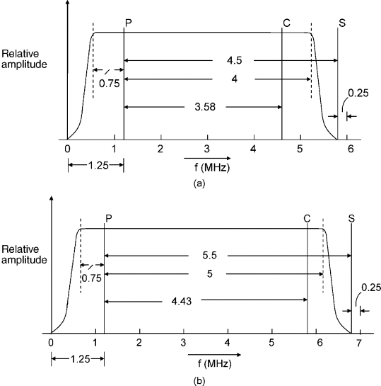
Figure 5.11 (a) NTSC TV standard signal and (b) PAL TV standard signal
The VSB signal can be generated by passing a DSB signal through an appropriate side band shaping filter, as shown in Figure 5.12. The demodulation scheme for the VSB signal is shown in Figure 5.13.
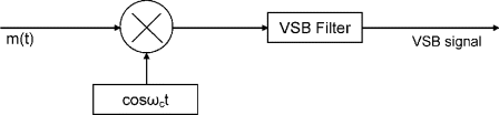
Figure 5.12 Generation of the VSB Signal
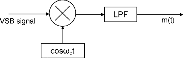
Figure 5.13 Demodulation of the VSB signal
5.3 Frequency Modulation
In frequency modulation (FM), the instantaneous frequency of the modulated signal varies directly as the instantaneous amplitude of the modulating or the base band signal. The rate at which these frequency variations take place is of course proportional to the modulating frequency. If the modulating signal is expressed by vm = Vm cos ωmt, then the instantaneous frequency f of an FM signal is mathematically expressed by
where
- fc = unmodulated carrier frequency
- Vm cos ωmt = instantaneous modulating voltage
- Vm = peak amplitude of the modulating signal
- ωm = modulating frequency
- K = constant of proportionality
The instantaneous frequency is maximum when cos ωmt = 1 and minimum when cos ωmt = − 1. This gives
where, fmax is the maximum instantaneous frequency and fmin is the minimum instantaneous frequency.
Frequency deviation (δ) is one of the important parameters of an FM signal and is given by (fmax − fc) or (fc − fmin). This gives
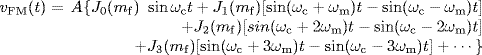
Figures 5.14 (a) to (c) show the modulating signal (taken as a single tone signal in this case), the unmodulated carrier and the modulated signal respectively. An FM signal can be mathematically represented by
where mf = modulation index = δ/fm. A is the amplitude of the modulated signal which in turn is equal to the amplitude of the carrier signal.

Figure 5.14 Frequency modulation
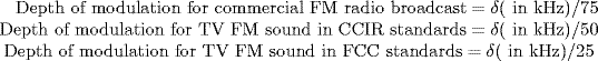
The depth of modulation in the case of an FM signal is defined as the ratio of the frequency deviation (δ) to the maximum allowable frequency deviation. The maximum allowable frequency deviation is different for different services and is also different for different standards, even for a given type of service using this form of modulation. For instance, the maximum allowable frequency deviation for a commercial FM radio broadcast is 75 kHz. It is 50 kHz for an FM signal of television sound in CCIR (Consultative Committee on International Radio) standards and 25 kHz for an FM signal of television sound in FCC (Federal communications commission) standards. Therefore,
5.3.1 Frequency Spectrum of the FM Signal
We have seen that an FM signal involves a sine of a sine. The solution of this expression involves the use of Bessel functions. The expression for the FM signal can be rewritten as
Thus the spectrum of an FM signal contains the carrier frequency component and apparently an infinite number of side bands. In general, Jn(mf) is the Bessel function of the first kind and nth order. It is evident from this expression that it is the value of mf and the value of the Bessel functions that will ultimately decide the number of side bands having significant amplitude and therefore bandwidth. Figure 5.15 shows how the carrier and side band amplitudes vary as a function of the modulation index. In fact, the curves shown in Figure 5.15 are nothing but plots of J0(mf), J1(mf), J2(mf), J3(mf), ... as a function of mf. Also, J0(mf), J1(mf), J2(mf), J3(mf), ... respectively represent the amplitudes of the carrier, the first side band, the second side band, the third side band and so on.
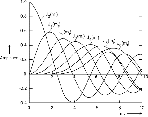
Figure 5.15 Variation of carrier and side band amplitudes as a function of the modulation index
The following observations can be made from this expression:
- For every modulating frequency, the FM signal contains an infinite number of side bands in addition to the carrier frequency. In an AM signal, there are only three frequency components, i.e. the carrier frequency, the lower side band frequency and the upper side band frequency.
- The modulation index (mf) determines the number of significant side bands. The higher the modulation index, the more the number of significant side bands. Figure 5.16 shows the spectra of FM signals for a given sinusoidal modulating signal for different values of the modulation index. As is evident from the figure, a higher modulation index leads to a larger number of side band frequency components having significant amplitude, i.e. side band frequency components having an appreciable relative amplitude.
- The side band distribution is symmetrical about the carrier frequency. The pair of side band frequencies for which the Bessel function has a negative value signifies a 180° phase change for that pair.
- In the case of an AM signal, when the modulation index increases so does the side band power and hence the transmitted power. In the case of an FM signal also, as the modulation index increases, the side band power increases. However, it does so only at the cost of carrier power so that the total transmitted power remains constant.
- In FM, the carrier component can disappear completely for certain specific values of mf for which J0(mf) becomes zero. These values are 2.4, 5.5, 8.6, 11.8 and so on.
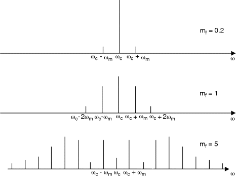
Figure 5.16 Spectra of FM signals for different values of the modulation index
5.3.2 Narrow Band and Wide Band FM
An FM signal, whether it is a narrow band FM signal or a wide band FM signal, is decided by its bandwidth and in turn by its modulation index. For a modulation index mf much less than 1, the signal is considered as the narrow band FM signal. It can be shown that for mf less than 0.2, 98 % of the normalized total signal power is contained within the bandwidth as given by:
where ωm is the sinusoidal modulating frequency.
In the case of an FM signal with an arbitrary modulating signal band limited to ωM, another parameter called the deviation ratio (D) can be defined as
The deviation ratio D has the same significance for arbitrary modulation as the modulation index mf for sinusoidal modulation. The bandwidth in this case is given by
This expression for bandwidth is generally referred to as Carson's rule.
In the case of D < 1, the FM signal is considered as narrow band signal and the bandwidth is given by the expression
In the case mf > 1 (for sinusoidal modulation) or D > 1 (for an arbitrary modulation signal band limited to ωM), the FM signal is termed as the wide band FM. The bandwidth of a wide band FM signal in the case of a sinosoidal modulating signal is given by
The bandwidth of a wide band FM signal in case of an arbitrary modulating signal band limited to ωM is given by
5.3.3 Noise in the FM Signal
It will be seen in the following paragraphs that frequency modulation is much less affected by the presence of noise as compared to the effect of noise on an amplitude modulated signal. Whenever a noise voltage with peak amplitude Vn is present along with a carrier voltage of peak amplitude Vc, the noise voltage amplitude modulates the carrier with a modulation index equal to Vn/Vc. It also phase modulates the carrier with a phase deviation equal to sin −1(Vn/Vc). This expression for phase deviation results when a single frequency noise voltage is considered vectorially and the noise voltage vector is superimposed on the carrier voltage vector, as shown in Figure 5.17. An FM receiver is not affected by the amplitude change as it can be removed in the limiter circuit inside the receiver. Also, an AM receiver will not be affected by the phase change. It is therefore the effect of phase change on the FM receiver and the effect of amplitude change on the AM receiver that can be used as the yardstick for determining the noise performance of the two modulation techniques. Two very important aspects that need to be addressed when the two communication techniques are compared vis-à-vis their noise performance are the effects of the modulation index and the signal-to-noise ratio at the receiver input. These are considered in the following paragraphs and are suitably illustrated with the help of examples.
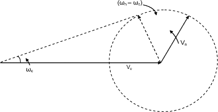
Figure 5.17 Effect of noise on signal
5.3.3.1 Effect of the Modulation Index
Let us take the case of noise voltage amplitude being one-fourth of the carrier amplitude. The carrier-to-noise voltage ratio of 4 is equivalent to the carrier-to-noise power ratio of 16 or 12 dB. The reasons for taking these figures will be obvious in the latter part of this section. A modulating frequency of 15 kHz is assumed, which is the highest possible frequency for voice communication. A modulation index of unity for both AM and FM is considered. In the case of an AM receiver, the noise-to-signal ratio will be 0.25 or 25 % as the noise voltage amplitude is one-fourth of the carrier voltage amplitude. In the case of an FM receiver, the noise-to-signal ratio will be 14.5°/57.3°(1 radian = 57.3o). This equals 0.253 or 25.3 %. Thus, when a signal-to-noise ratio of 12 dB and a unity modulation index for AM and FM systems is assumed, the noise performance of the two systems is more or less the same, slightly better in the case of the AM system.
The effect of change in modulating noise frequencies will now be examined. It should be remembered that the noise frequency will interfere with the desired signals only when the noise difference frequency, that is the frequency produced by the mixing action of the carrier and noise frequencies, lies within the pass band of the receiver. A change in modulating and noise difference frequencies does not have any effect on the noise modulation index and signal modulation index in the case of AM. As a result, the noise-to-signal ratio in the case of AM remains unaltered. In the case of FM, when the noise difference frequency is lowered, there again is no effect of this change on the noise modulation index as a constant noise-to-carrier voltage means a constant phase modulation due to noise and hence a constant noise modulation index. However, a reduction in modulating frequency implies an increase in the signal modulation index in the same proportion. This leads to a reduction in the noise-to-signal ratio in the same proportion. For instance, in the example considered earlier, if the modulating frequency is decreased from 15 kHz to 30 Hz, the noise-to-signal ratio in the case of FM will reduce to (0.253 × 30/15000) = 0.0005 or 0.05 %, while the noise-to-signal ratio in the case of AM remains the same at 0.25 or 25 %.
Figure 5.18 shows how noise at the receiver output varies with the noise difference frequency or noise side band frequency assuming that noise frequencies are evenly spread over the entire pass band of the receiver. Figure 5.18 (a) is for the case where mf = 1 at the highest modulating frequency and Figure 5.18 (b) depicts the case where mf = 5 at the highest modulating frequency. A rectangular distribution in the case of AM is obvious.
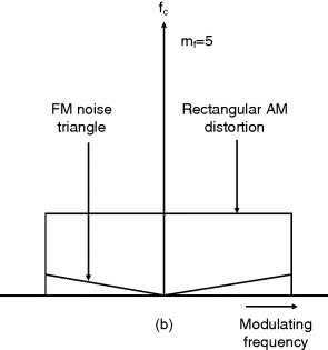
Figure 5.18 (a) Noise in the FM and AM signals for the modulation index equal to 1. (b) Noise in FM and AM signals for the modulation index equal to 5
5.3.3.2 Effect of the Signal-to-Noise Ratio
An FM receiver uses a limiter circuit that precedes the FM demodulator. The idea behind the use of a limiter circuit is the fact that any amplitude variations in an FM signal are spurious and contain no intelligence information. Since FM demodulator circuits to some extent respond to amplitude variations, removing these amplitude variations results in a better noise performance in an FM receiver. The amplitude limiter acts on the stronger signals and tends to reject the weaker signals. Thus when the signal-to-noise ratio at the limiter input is very low, that is when the signal is weak, the FM system offers a poorer performance as compared to an AM system. The FM system offers a better performance with respect to an AM system only when the signal-to-noise ratio is above a certain threshold value, which is 8 dB (or 9 dB). This is depicted in Figure 5.19. It is clear from the curves shown in Figure 5.19, the FM system offers full improvement over the AM system when the signal-to-noise ratio is about 3 dB greater than this threshold of 9 dB. It is evident from Figure 5.19 that the AM system has a definite advantage as compared to the FM system for an input signal-to-noise ratio less than 9 dB. Improvement of the FM system over the AM system is visible for an input signal-to-noise ratio greater than 9dB. The quantum of improvement increases with an increase in the signal-to-noise ratio until it reaches its maximum value at the signal-to-noise ratio of 12 dB. From then onwards, FM offers this maximum improvement over AM. It may be mentioned that the first threshold (point X) represents a modulation index (mf) of unity and the second threshold (point Y) corresponds to a modulation index (mf) equal to the deviation ratio, which is the ratio of maximum frequency deviation to maximum modulating frequency.

Figure 5.19 Signal-to-noise ratio in FM and AM systems
In summary, it can be stated that an FM system offers a better performance than an AM system provided:
- The modulation index is greater than unity.
- The amplitude of the carrier is greater than the maximum noise peak amplitudes.
- The receiver is insensitive to amplitude variations.
5.3.3.3 Pre-emphasis and De-emphasis
In the case of FM, noise has a greater effect on higher modulating frequencies than it has on lower ones. This is because of the fact that FM results in smaller values of phase deviation at the higher modulating frequencies whereas the phase deviation due to white noise is constant for all frequencies. Due to this, the signal-to-noise ratio deteriorates at higher modulating frequencies. If the higher modulating frequencies above a certain cut-off frequency were boosted at the transmitter prior to modulation according to a certain known curve and then reduced at the receiver in the same fashion after the demodulator, a definite improvement in noise immunity would result. The process of boosting the higher modulating frequencies at the transmitter and then reducing them in the receiver are respectively known as pre-emphasis and de-emphasis. Figure 5.20 shows the pre-emphasis and de-emphasis curves.
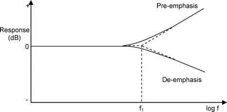
Figure 5.20 Pre-emphasis and de-emphasis curves
Having discussed various aspects of noise performance of an FM system, it would be worthwhile presenting the mathematical expression that could be used to compute the base band signal-to-noise ratio at the output of the demodulator. Without getting into intricate mathematics, the following expression can be written for the base band signal-to-noise ratio (Sb/Nb):
where
- fd = frequency deviation
- fm = highest modulating frequency
- B = receiver bandwidth
- C = carrier power at the receiver input
- N = noise power (kTB) in bandwidth (B)
The above expression does not take into account the improvement due to the use of pre-emphasis and de-emphasis. In that case the expression is modified to
where f1 = cut-off frequency for the pre-emphasis/de-emphasis curve.
5.3.4 Generation of FM Signals
In the case of an FM signal, the instantaneous frequency of the modulated signal varies directly as the instantaneous amplitude of the modulating or base band signal. The rate at which these frequency variations take place is of course proportional to the modulating frequency. Though there are many possible schemes that can be used to generate the signal characterized above, all of them depend simply on varying the frequency of an oscillator circuit in accordance with the modulating signal input.
One of the possible methods is based on the use of a varactor (a voltage variable capacitor) as a part of the tuned circuit of an L–C oscillator. The resonant frequency of this oscillator will not vary directly with the amplitude of the modulating frequency as it is inversely proportional to the square root of the capacitance. However, if the frequency deviation is kept small, the resulting FM signal is quite linear. Figure 5.21 shows the typical arrangement when the modulating signal is an audio signal. This is also known as the direct method of generating an FM signal, as in this case the modulating signal directly controls the carrier frequency.
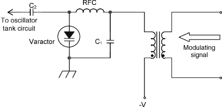
Figure 5.21 L–C oscillator based direct method of FM signal generation
Another direct method scheme that can be used for generation of an FM signal is the reactance modulator. In this, the reactance offered by a three-terminal active device such as an field effect transistor (FET) or a bipolar junction transistor (BJT) forms a part of the tuned circuit of the oscillator. The reactance in this case is made to vary in accordance with the modulating signal applied to the relevant terminal of the active device. For example, in the case of FET, the drain source reactance can be shown to be proportional to the transconductance of the device, which in turn can be made to depend upon the bias voltage at its gate terminal. The main advantage of using the reactance modulator is that large frequency deviations are possible and thus less frequency multiplication is required. One of the major disadvantages of both these direct method schemes is that carrier frequency tends to drift and therefore additional circuitry is required for frequency stabilization. The problem of frequency drift is overcome in crystal controlled oscillator schemes.
Although it is known that crystal control provides a very stable operating frequency, the exact frequency of oscillation in this case mainly depends upon the crystal characteristics and to a very small extent on the external circuit. For example, a capacitor connected across the crystal can be used to change its frequency, typically from 0.001 % to 0.005 %. The frequency change may be linear only up to a change of 0.001 %. Thus a crystal oscillator can be frequency modulated over a very small range by a parallel varactor. The frequency deviation possible with such a scheme is usually too small to be used directly. The frequency deviation in this case is then increased by using frequency multipliers as shown in Figure 5.22.
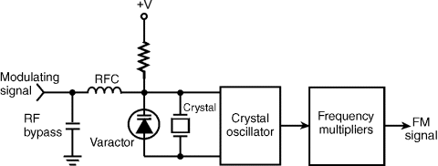
Figure 5.22 Crystal oscillator based scheme for FM signal generation
Another approach that eliminates the requirement of extensive chains of frequency multipliers is an indirect method where frequency deviation is not introduced at the source of the RF carrier signal, that is the oscillator. The oscillator in this case is crystal controlled to get the desired stability of the unmodulated carrier frequency and the frequency deviation is introduced at a later stage. The modulating signal phase modulates the RF carrier signal produced by the crystal controlled oscillator. Since, frequency is simply the rate of change of phase, phase modulation of the carrier has an associated frequency modulation. Introduction of a leading phase shift would lead to an increase in the RF carrier frequency and a lagging phase shift results in a reduced RF carrier frequency. Thus, if the phase of the RF carrier is shifted by the modulating signal in a proper way, the result is a frequency modulated signal. Since phase modulation also produces little frequency deviation, a frequency multiplier chain is required in this case too. Figure 5.23 shows the typical schematic arrangement for generating an FM signal via the phase modulation route.

Figure 5.23 Indirect method of generating an FM signal by employing phase modulation
5.3.5 Detection of FM Signals
Detection of an FM signal involves the use of some kind of frequency discriminator circuit that can generate an electrical output directly proportional to the frequency deviation from the unmodulated RF carrier frequency. The simplest of the possible circuits would be the balanced slope detector, which makes use of two resonant circuits, one off-tuned to one side of the unmodulated RF carrier frequency and the other off-tuned to the other side of it. Figure 5.24 shows the basic circuit. When the input to this circuit is at the unmodulated carrier frequency, the two off-tuned slope detectors (or the resonant circuits) produce equal amplitude but out-of-phase outputs across them. The two signals, after passing through their respective diodes, produce equal amplitude opposing DC outputs, which combine together to produce a zero or near-zero output. When the received signal frequency is towards either side of the centre frequency, one output has a higher amplitude than the other to produce a net DC output across the load. The polarity of the output produced depends on which side of the centre frequency the received signal is. Figure 5.25 explains all of this. Such a detector circuit, however, does not find application for voice communication because of its poor response linearity.

Figure 5.24 Basic circuit of the balanced slope detector (IF, intermediate frequency)
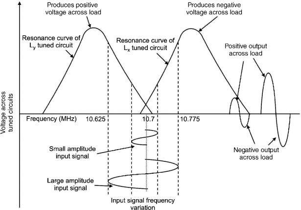
Figure 5.25 Output of the balanced slope detector
Another class of FM detectors, known as quadrature detectors, use a combination of two quadrature signals, i.e. two signals 90° out of phase, to obtain the frequency discrimination property. One of the two signals is the FM signal to be detected and its quadrature counterpart is generated by using either a capacitor or an inductor, as shown in Figure 5.26. The two signals here have been labelled Ea and Eb.

Figure 5.26 Generation of the quadrature signal
If the secondary of the transformer in the arrangements of Figure 5.26 is tuned to the unmodulated carrier frequency, then at this frequency, Ea and Eb are 90° out of phase, as shown in Figure 5.27 (a). The phase difference between Ea and Eb is greater than 90° when the input frequency is less than the unmodulated carrier frequency [Figure 5.27 (b)] and less than 90°, in case the input frequency is greater than the unmodulated carrier frequency [Figure 5.27 (c)]. The resultant is a signal that is proportional to EaEb cos ϕ, where ϕ is the phase deviation from 90°. This in fact forms the basis of two of the most commonly used FM detectors, namely the Foster–Seeley frequency discriminator and the ratio detector.
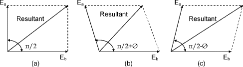
Figure 5.27 Phase diagrams of FM signals
In the Foster–Seeley frequency discriminator circuit of Figure 5.28 (a), the two quadrature signals are provided by the primary signal (Ep) as appearing at the centre tap of secondary and Eb. It should be appreciated that Ea and Eb are 180° out of phase and also that Ep, available at the centre tap of the secondary, is 90° out of phase with the total secondary signal. Signals E1 and E2 appearing across the two halves of the secondary have equal amplitudes when the received signal is at the unmodulated carrier frequency as shown in the phasor diagrams Figure 5.28 (b). E1 and E2 cause rectified currents I1 and I2 to flow in the opposite directions, with the result that voltage across R1 and R2 are equal and opposite. The detected voltage is zero for R1 = R2. The conditions when the received signal frequency deviates from the unmodulated carrier frequency value are also shown in the phasor diagrams. In the case of frequency deviation, there is a net output voltage whose amplitude and polarity depends upon the amplitude and sense of frequency deviation. The frequency response curve for this type of FM discriminator circuit is also given in the Figure 5.28 (c).
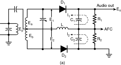


Figure 5.28 Foster–Seeley frequency discriminator (AFC, automatic frequency control)
Another commonly used FM detector circuit is the ratio detector. This circuit has the advantage that it is insensitive to short term amplitude fluctuations in the carrier and therefore does not require an additional limiter circuit. The circuit configuration, as shown in Figure 5.29, is similar to the one given in the Foster–Seeley frequency discriminator circuit except for a couple of changes. These are a reversal of diode connections and the addition of a large capacitor (C5). The time constant (R1 + R2)C5 is much larger than the time period of even the lowest modulating frequency of interest. The detected signal in this case appears across the C3–C4 junction. The sum output across R1–R2 and hence across C3–C4 remains constant for a given carrier level and is also insensitive to rapid fluctuations in the carrier level. However, if the carrier level changes very slowly, C5 charges or discharges to the new carrier level. The detected signal is therefore not only proportional to the frequency deviation but also depends upon the average carrier level.

Figure 5.29 Ratio detector
Yet another form of FM detector is the one implemented using a phase locked loop (PLL). A PLL has a phase detector (usually a double balanced mixer), a lowpass filter and an error amplifier in the forward path and a voltage controlled oscillator (VCO) in the feedback path. The detected output appears at the output of the error amplifier, as shown in Figure 5.30. A PLL-based FM detector functions as follows.
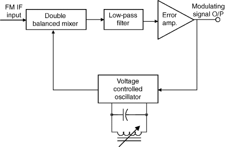
Figure 5.30 PLL based FM detector
The FM signal is applied to the input of the phase detector. The VCO is tuned to a nominal frequency equal to the unmodulated carrier frequency. The phase detector produces an error voltage depending upon the frequency and phase difference between the VCO output and the instantaneous frequency of the input FM signal. As the input frequency deviates from the centre frequency, the error voltage produced as a result of frequency difference after passing through the lowpass filter and error amplifier drives the control input of the VCO to keep its output frequency always in lock with the instantaneous frequency of the input FM signal. As a result, the error amplifier always represents the detected output. The double balanced mixer nature of the phase detector suppresses any carrier level changes and therefore the PLL-based FM detector requires no additional limiter circuit.
A comparison of the three types of FM detector reveals that the Foster–Seeley type frequency discriminator offers excellent linearity of response, is easy to balance and the detected output depends only on the frequency deviation. However, it needs high gain RF and IF stages to ensure limiting action. The ratio detector circuit, on the other hand, requires no additional limiter circuit; detected output depends both on the frequency deviation as well as on the average carrier level. However, it is difficult to balance. The PLL-based FM detector offers excellent reproduction of the modulating signal, is easy to balance and has low cost and high reliability.
5.4 Pulse Communication Systems
Pulse communication systems differ from continuous wave communication systems in the sense that the message signal or intelligence to be transmitted is not supplied continuously as in the case of AM or FM. In this case, it is sampled at regular intervals and it is the sampled data that is transmitted. All pulse communication systems fall into either of two categories, namely analogue pulse communication systems and digital pulse communication systems. Analogue and digital pulse communication systems differ in the mode of transmission of sampled information. In the case of analogue pulse communication systems, representation of the sampled amplitude may be infinitely variable whereas in the case of digital pulse communication systems, a code representing the sampled amplitude to the nearest predetermined level is transmitted.
5.4.1 Analogue Pulse Communication Systems
Important techniques that fall into the category of analogue pulse communication systems include:
- Pulse amplitude modulation
- Pulse width (or duration) modulation
- Pulse position modulation
5.4.1.1 Pulse Amplitude Modulation
In the case of pulse amplitude modulation (PAM), the signal is sampled at regular intervals and the amplitude of each sample, which is a pulse, is proportional to the amplitude of the modulating signal at the time instant of sampling. The samples, shown in Figure 5.31, can have either a positive or negative polarity. In a single polarity PAM, a fixed DC level can be added to the signal, as shown in Figure 5.31 (c). These samples can then be transmitted either by a cable or used to modulate a carrier for wireless transmission. Frequency modulation is usually employed for the purpose and the system is known as PAM-FM.
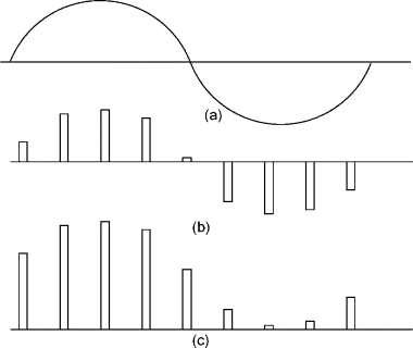
Figure 5.31 Pulse amplitude modulation
5.4.1.2 Pulse Width Modulation
In the case of pulse width modulation (PWM), as shown in Figure 5.32, the starting time of the sampled pulses and their amplitude is fixed. The width of each pulse is proportional to the amplitude of the modulating signal at the sampling time instant.
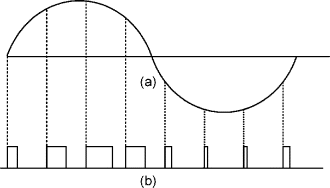
Figure 5.32 Pulse width modulation
5.4.1.3 Pulse Position Modulation
In the case of pulse position modulation (PPM), the amplitude and width of the sampled pulses is maintained as constant and the position of each pulse with respect to the position of a recurrent reference pulse varies as a function of the instantaneous sampled amplitude of the modulating signal. In this case, the transmitter sends synchronizing pulses to operate timing circuits in the receiver.
A pulse position modulated signal can be generated from a pulse width modulated signal. In a PWM signal, the position of the leading edges is fixed whereas that of the trailing edges depends upon the width of the pulse, which in turn is proportional to the amplitude of the modulating signal at the time instant of sampling. Quite obviously, the trailing edges constitute the pulse position modulated signal. The sequence of trailing edges can be obtained by differentiating the PWM signal and then clipping the leading edges as shown in Figure 5.33. Pulse width modulation and pulse position modulation both fall into the category of pulse time modulation (PTM).

Figure 5.33 Pulse position modulation
5.4.2 Digital Pulse Communication Systems
Digital pulse communication techniques differ from analogue pulse communication techniques described in the previous paragraphs in the sense that in the case of analogue pulse modulation the sampling process transforms the modulating signal into a train of pulses, with each pulse in the pulse train representing the sampled amplitude at that instant of time. It is one of the characteristic features of the pulse, such as amplitude in the case of PAM, width in the case of PWM and position of leading or trailing edges in the case of PPM, that is varied in accordance with the amplitude of the modulating signal. What is important to note here is that the characteristic parameter of the pulse, which is amplitude or width or position, is infinitely variable. As an illustration, if in the case of pulse width modulation, every volt of modulating signal amplitude corresponded to 1 μs of pulse width, then 5.23 volt and 5.24 volt amplitudes would be represented by 5.23μs and 5.24 μs respectively. Further, there could be any number of amplitudes between 5.23 volts and 5.24 volts. It is not the same in the case of digital pulse communication techniques, to be discussed in the paragraphs to follow, where each sampled amplitude is transmitted by a digital code representing the nearest predetermined level.
Important techniques that fall into the category of digital pulse communication systems include:
- Pulse code modulation (PCM)
- Differential PCM
- Delta modulation
- Adaptive delta modulation
5.4.2.1 Pulse Code Modulation
In pulse code modulation (PCM), the peak-to-peak amplitude range of the modulating signal is divided into a number of standard levels, which in the case of a binary system is an integral power of 2. The amplitude of the signal to be sent at any sampling instant is the nearest standard level. For example, if at a particular sampling instant, the signal amplitude is 3.2 volts, it will not be sent as a 3.2 volt pulse, as might have been the case with PAM, or a 3.2 μs wide pulse, as for the case with PWM; instead it will be sent as the digit 3, if 3 volts is the nearest standard amplitude. If the signal range has been divided into 128 levels, it will be transmitted as 0000011. The coded waveform would be like that shown in Figure 5.34 (a). This process is known as quantizing. In fact, a supervisory pulse is also added with each code group to facilitate reception. Thus, the number of bits for 2n chosen standard levels per code group is n + 1. Figure 5.34 (b) illustrates the quantizing process in PCM.
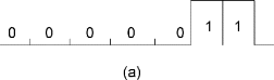
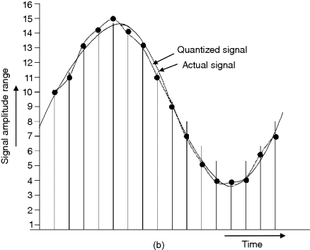
Figure 5.34 Quantizing process
It is evident from Figure 5.34 (b) that the quantizing process distorts the signal. This distortion is referred to as quantization noise, which is random in nature as the error in the signal's amplitude and that actually sent after quantization is random. The maximum error can be as high as half of the sampling interval, which means that if the number of levels used were 16, it would be 1/32 of the total signal amplitude range. It should be mentioned here that it would be unfair to say that a PCM system with 16 standard levels will necessarily have a signal-to-quantizing noise ratio of 32:1, as neither the signal nor the quantizing noise will always have its maximum value. The signal-to-noise ratio also depends upon many other factors and also its dependence on the number of quantizing levels is statistical in nature. Nevertheless, an increase in the number of standard levels leads to an increase in the signal-to-noise ratio. In practice, for speech signals, 128 levels are considered as adequate. In addition, the more the number of levels, the larger is the number of bits to be transmitted and therefore higher is the required bandwidth.
In binary PCM, where the binary system of representation is used for encoding various sampled amplitudes, the number of bits to be transmitted per second would be given by nfs, where
- n = log2L
- L = number of standard levels
and
Assuming that the PCM signal is a lowpass signal of bandwidth fPCM, then the required minimum sampling rate would be 2fPCM. Therefore,
Generating a PCM signal is a complex process. The message signal is usually sampled and first converted into a PAM signal, which is then quantized and encoded. The encoded signal can then be transmitted either directly via a cable or used to modulate a carrier using analogue or digital modulation techniques. PCM-AM is quite common.
5.4.2.2 Differential PCM
Differential PCM is similar to conventional PCM. The difference between the two lies in the fact that in differential PCM, each word or code group indicates a difference in amplitude (positive or negative) between the current sample and the immediately preceding one. Thus, it is not the absolute but the relative value that is indicated. As a consequence, the bandwidth required is less as compared to the one required in case of normal PCM.
5.4.2.3 Delta Modulation
Delta modulation (DM) has various forms. In one of the simplest forms, only one bit is transmitted per sample just to indicate whether the amplitude of the current sample is greater or smaller than the amplitude of the immediately preceding sample. It has extremely simple encoding and decoding processes but then it may result in tremendous quantizing noise in case of rapidly varying signals.
Figure 5.35 (a) shows a simple delta modulator system. The message signal m(t) is added to a reference signal with the polarity shown. The reference signal is an integral part of the delta modulated signal. The error signal e(t) so produced is fed to a comparator. The output of the comparator is (+ Δ) for e(t) > 0 and (− Δ) for e(t) < 0. The output of the delta modulator is a series of impulses with the polarity of each impulse depending upon the sign of e(t) at the sampling instants of time. Integration of the delta modulated output xDM(t) is a staircase approximation of the message signal m(t), as shown in Figure 5.35 (b).

Figure 5.35 (a) Delta modulator system. (b) Output waveform of a delta modulator system
A delta modulated signal can be demodulated by integrating the modulated signal to obtain the staircase approximation and then passing it through a lowpass filter. The smaller the step size (Δ), the better is the reproduction of the message signal. However, a small step size must be accompanied by a higher sampling rate if the slope overload phenomenon is to be avoided. In fact, to avoid slope overload and associated signal distortion, the following condition should be satisfied:
where Ts = time between successive sampling time instants.
5.4.2.4 Adaptive Delta Modulator
This is a type of delta modulator. In delta modulation, the dynamic range of amplitude of the message signal m(t) is very small due to threshold and overload effects. This problem is overcome in an adaptive delta modulator. In adaptive delta modulation, the step size (Δ) is varied according to the level of the message signal. The step size is increased as the slope of the message signal increases to avoid overload. The step size is reduced to reduce the threshold level and hence the quantizing noise when the message signal slope is small. In the case of adaptive delta modulation, however, the receiver also needs to be adaptive. The step size at the receiver should also be made to change to match the changes in step size at the transmitter.
5.5 Sampling Theorem
During the discussion on digital pulse communication techniques such as pulse code modulation, delta modulation, etc., it was noted that the three essential processes of such a system are sampling, quantizing and encoding. Sampling is the process in which a continuous time signal is sampled at discrete instants of time and its amplitudes at those discrete instants of time are measured. Quantization is the process by which the sampled amplitudes are represented in the form of a finite set of levels. The encoding process designates each quantized level by a code.
Digital transmission of analogue signals has been made possible by sampling the continuous time signal at a certain minimum rate, which is dictated by what is called the sampling theorem. The sampling theorem states that a band limited signal with the highest frequency component as fM Hz, can be recovered completely from a set of samples taken at a rate of fs samples per second, provided that fs ≥ 2fM. This theorem is also known as the uniform sampling theorem for base band or lowpass signals. The minimum sampling rate of 2fM samples per second is called the Nyquist rate and its reciprocal the Nyquist interval. For sampling bandpass signals, lower sampling rates can sometimes be used.
The sampling theorem for bandpass signals states that if a bandpass message signal has a bandwidth of fB and an upper frequency limit of fu, then the signal can be recovered from the sampled signal by bandpass filtering if fs = 2fu/k, where fs is the sampling rate and k is the largest integer not exceeding fu/fB.
5.6 Shannon–Hartley Theorem
The Shannon–Hartley theorem describes the capacity of a noisy channel (assuming that the noise is random). According to this theorem,
where
- C = channel capacity in bps
- B = channel bandwidth in Hz
- S/N = signal-to-noise ratio at the channel output or receiver input
The Shannon–Hartley theorem underlines the fundamental importance of bandwidth and signal-to-noise ratio in communication. It also shows that for a given channel capacity, increased bandwidth can be exchanged for decreased signal power. It should be mentioned that increasing the channel bandwidth by a certain factor does not increase the channel capacity by the same factor in a noisy channel, as would apparently be suggested by the Shannon–Hartley theorem. This is because increasing the bandwidth also increases noise, thus decreasing the signal-to-noise ratio. However, channel capacity does increase with an increase in bandwidth; the increase will not be in the same proportion.
5.7 Digital Modulation Techniques
Base band digital signals have significant power content in the lower part of the frequency spectrum. Because of this, these signals can be conveniently transmitted over a pair of wires or coaxial cables. At the same time, for the same reason, it is not possible to have efficient wireless transmission of base band signals as it would require prohibitively large antennas, which would not be a practical or a feasible proposition. Therefore, if base band digital signals are to be transmitted over a wireless communication link, they should first modulate a continuous wave (CW) high frequency carrier. Three well-known techniques available for the purpose include:
- Amplitude shift keying (ASK)
- Frequency shift keying (FSK)
- Phase shift keying (PSK)
Each one of these is described in the following paragraphs. Of the three techniques used for digital carrier modulation, PSK and its various derivatives, like differential PSK (DPSK), quadrature PSK (QPSK) and offset quadrature PSK (O-QPSK), are the most commonly used ones, more so for satellite communications, because of certain advantages they offer over others. PSK is therefore described in a little more detail.
5.7.1 Amplitude Shift Keying (ASK)
In the simplest form of amplitude shift keying (ASK), the carrier signal is switched ON and OFF depending on whether a ‘1’ or ‘0’ is to be transmitted (Figure 5.36). For obvious reasons, this form of ASK is also known as ON–OFF keying (OOK). The signal in this case is represented by
The ON–OFF keying has the disadvantage that appearance of any noise during transmission of bit ‘0’ can be misinterpreted as data. This problem can be overcome by switching the amplitude of the carrier between two amplitudes, one representing a ‘1’ and the other representing a ‘0’, as shown in Figure 5.37. Again, the carrier can be suppressed to have maximum power in information carrying signals and also one of the side bands can be filtered out to conserve the bandwidth.
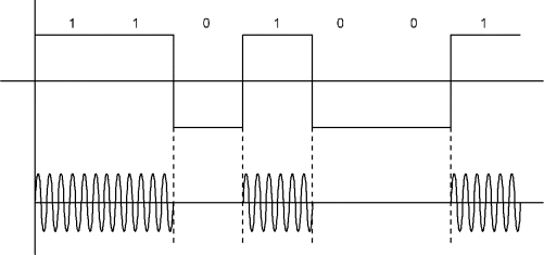
Figure 5.36 Amplitude shift keying
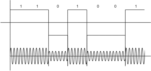
Figure 5.37 Two level amplitude shift keying
5.7.2 Frequency Shift Keying (FSK)
In frequency shift keying (FSK), it is the frequency of the carrier signal that is switched between two values, one representing bit ‘1’ and the other representing bit ‘0’, as shown in Figure 5.38. The modulated signal in this case is represented by


Figure 5.38 Frequency shift keying
In the case of FSK, when the modulation rate increases, the difference between the two chosen frequencies to represent a ‘1’ and a ‘0’ also needs to be higher. Keeping in mind the restriction in available bandwidth, it would not be possible to achieve a bit transmission rate beyond a certain value.
5.7.3 Phase Shift Keying (PSK)
In phase shift keying (PSK), the phase of the carrier is discretely varied with respect to either a reference phase or to the phase of the immediately preceding signal element in accordance with the data being transmitted. For example, when encoding bits, the phase shift could be 0° for encoding a bit ‘0’ and 180° for encoding a bit ‘1’, as shown in Figure 5.39. The phase shift could have been −90° for encoding a bit ‘0’ and +90° for encoding a bit ‘1'. The essence is that representations for ‘0’ and ‘1’ are a total of 180° apart. Such PSK systems in which the carrier can assume only two different phase angles are known as binary phase shift keying (BPSK) systems. In the BPSK system, each phase change carries one bit of information. This, in other words, means that the bit rate equals the modulation rate. Now, if the number of recognizable phase angles is increased to 4, then two bits of information could be encoded into each signal element.
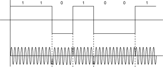
Figure 5.39 Binary phase shift keying
Returning to the subject of BPSK, the carrier signals used to represent ‘0’ and ‘1’ bits could be expressed by equations 5.34(a) and 5.34(b) respectively.
Since the phase difference between two carrier signals is 180°, i.e. θ1 = θ0 + 180°, then
5.7.4 Differential Phase Shift Keying (DPSK)
Another form of PSK is differential PSK (DPSK). In DPSK instead of instantaneous phase of the modulated signal determining which bit is transmitted, it is the change in phase that carries message intelligence. In this system, one logic level (say ‘1') represents a change in phase of the modulated signal and the other logic level (i.e. ‘0') represents no change in phase. In other words, if a digit changes in the bit stream from 0 to 1 or from 1 to 0, a ‘1’ is transmitted in the form of change in phase of the modulated signal. In the case where there is no change, a ‘0’ is transmitted in the form of no phase change in the modulated signal.
The BPSK signal is detected using a coherent demodulator where a locally generated carrier component is extracted from the received signal by a PLL circuit. This locally generated carrier assists in the product demodulation process where the product of the carrier and the received modulated signal generates the demodulated output. There could be a difficulty in successfully identifying the correct phase of the regenerated signal for demodulation. Differential PSK takes care of this ambiguity to a large extent.
5.7.5 Quadrature Phase Shift Keying (QPSK)
Quadrature phase shift keying (QPSK) is the most commonly used form of PSK. A QPSK modulator is nothing but two BPSK modulators operating in quadrature. The input bit stream (d0, d1, d2, d3, d4, ...) representing the message signal is split into two bit streams, one having, say, even numbered bits (d0, d2, d4, ...) and the other having odd numbered bits (d1, d3, d5, ...). Also, in QPSK, if each pulse in the input bit stream has a duration of T seconds, then each pulse in the even/odd numbered bit streams has a pulse duration of 2T seconds, as shown in Figure 5.40.
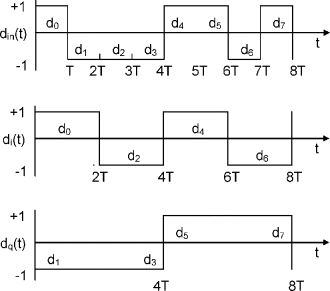
Figure 5.40 Quadrature phase shift keying
Figure 5.41 shows the block schematic arrangement of a typical QPSK modulator. One of the bit streams [di(t)] feeds the in-phase modulator while the other bit stream [dq(t)] feeds the quadrature modulator. The modulator output can be written as
This expression can also be written in a simplified form as
In the input bit stream shown in Figure 5.40, an amplitude of +1 represents a bit ‘1’ and an amplitude of −1 represents a bit ‘0'. The in-phase bit stream represented by di(t) modulates the cosine function and has the effect of shifting the phase of the function by 0 or π radians. This is equivalent to BPSK. The other pulse stream represented by dq(t) modulates the sine function, thus producing another BPSK-like output that is orthogonal to the one produced by di(t). The vector sum of the two produces a QPSK signal, given by
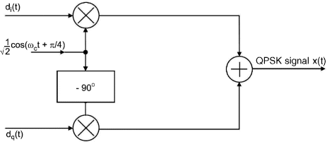
Figure 5.41 Block schematic arrangement of a typical QPSK modulator
Figure 5.42 illustrates this further.
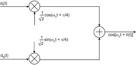
Figure 5.42 Conceptual diagram of QPSK
Depending on the status of the pair of bits having one bit from the di(t) bit stream and the other from the dq(t) bit stream, θ(t) will have any of the four values of 0°, 90°, 180° and 270°. Four possible combinations are 00, 01, 10 and 11. Figure 5.43 illustrates the process further. It shows all four possible phase states. The in-phase bits operate on the vertical axis at phase states of 90° and 270° whereas the quadrature phase channel operates on the horizontal axis at phase states of 0° and 180°. The vector sum of the two produces each of the four phase states as shown. As mentioned earlier, the phase state of the QPSK modulator output depends on a pair of bits. The phase states in the present case would be 0°, 90°, 180° and 270° for input combinations 11, 10, 00 and 01 respectively.
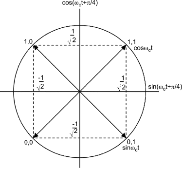
Figure 5.43 QPSK phase diagram
Since each symbol in QPSK comprises two bits, the symbol transmission rate is half of the bit transmission rate of BPSK and the bandwidth requirement is halved. The power spectrum for QPSK is the same as that for BPSK.
5.7.6 Offset QPSK
The offset QPSK is similar to QPSK with the difference that the alignment of the odd/even streams is shifted by an offset equal to T seconds, as shown in Figure 5.44. In the case of QPSK, as explained earlier, a carrier phase change can occur every 2T seconds. If neither of the two streams changes sign, the carrier phase remains unaltered. If only one of them changes sign, the carrier phase undergoes a change of +90° or −90° and if both change sign, the carrier phase undergoes a change of 180°. In such a situation, the QPSK signal no longer has a constant envelope if it is filtered to remove the spectral side lobes. If such a QPSK signal is passed through a nonlinear amplifier, the amplitude variations could cause spectral spreading to restore unwanted side lobes, which in turn could lead to interference problems. Offset QPSK overcomes this problem. Due to staggering in-phase and quadrature-phase bit streams, the possibility of the carrier phase changing state by 180° is eliminated as only one bit stream can change state at any time instant of transition. A phase change of +90° or −90° does cause a small drop in the envelope, but it does not fall to near zero as in the case of QPSK for a 180° phase change.

Figure 5.44 Offset QPSK waveform
5.7.7 8PSK and 16PSK
8PSK and 16PSK digital modulation techniques are an extension of QPSK. While in QPSK there are four different defined phase positions allowing each symbol to be represented by two bits, in the case of 8PSK and 16PSK there are 8 and 16 defined phase changes, respectively. Each phase change is represented by three bits for 8PSK while for 16PSK each phase change is represented by four bits. In other words, 8PSK employs eight symbols with constant carrier amplitude and a phase shift of 45° between adjacent phase states and 16PSK employs 16 symbols with constant amplitude carrier signal and a phase shift of 22.5°. While 8PSK transmits three bits per symbol, 16PSK transmits four bits per symbol. Consequently, for the same bandwidth specification or symbol rate, data bit rates for 8PSK and 16PSK are, respectively, three and four times conventional BPSK. When compared to QPSK, these rates are 50 % higher for 8PSK and 100 % higher for 16PSK. Figures 5.45 (a) and (b) show I-Q phase diagrams for 8PSK and 16PSK, respectively.

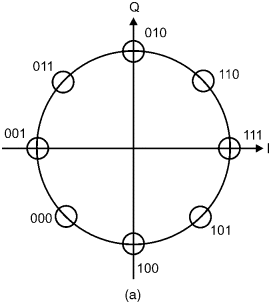
Figure 5.45 I-Q phase diagram: (a) 8PSK and (b) 16PSK
Multiple phase shift keying (M-PSK) digital modulation techniques such as 8PSK and 16PSK have the advantage of being spectrally very efficient. Another advantage is that a constant amplitude carrier allows the use of power efficient non-linear amplifiers such as class-C amplifiers. For a given bandwidth, 8PSK and 16PSK offer increased data capacity at the same bit error rate. The disadvantage is that a greater number of relatively smaller phase shifts makes the demodulation process very complex, more so in the presence of noise and interference. When the distance between different positions on the I-Q phase diagram is shorter there is increased risk of the symbols being misinterpreted. This requires additional error coding bits, which effectively reduces data throughput of the required data.
One common example of the use of the 8PSK technique is in enhanced data rate for global evolution (EDGE) technology. EDGE is a technology that can be used to enhance the data rate of existing global systems for mobile communications (GSMs) and digital-advanced mobile phone system (D-AMPS) communication networks. Both GSM and D-AMPS are second generation mobile communication systems. EDGE is an official member of the IMT-2000 family and in Europe it is seen as an intermediate technology for transition of 2G mobile communication systems like GSM to 3G systems like the universal mobile telecommunication system (UMTS).
5.7.8 Quadrature Amplitude Modulation (QAM)
M-PSK modulation techniques such as 8PSK and 16PSK achieve a higher bit rate for a given symbol rate by having larger number of phase positions of the constant amplitude carrier signal. As the number of phase positions increases further beyond 8 or 16 in an M-PSK system, the distance between adjacent phase positions reduces to a point where the advantage of increased bit rate is outweighed by increased demodulation complexity and bit error rate. In the case of 32PSK and 64PSK, the phase shifts between two adjacent positions are 11.25° and 5.625°. Quadrature amplitude modulation (QAM) is a method of increasing the bit rate for a given symbol rate without causing a significant reduction in phase shift between adjacent phase positions.
QAM is a combination of amplitude and phase shift keying modulation techniques, that is, it makes use of both phase shifts as well as amplitude variations to increase the bit rate. For example, 8QAM makes use of four carrier signal phases and two different amplitude levels. Other variations of QAM are 16QAM, 32QAM, 64QAM, 128QAM and 256QAM. Figures 5.46 (a) and (b) show I-Q phase diagrams of 16QAM in circular and rectangular configurations respectively. The phase diagram of Figure 5.46 (a) has eight different phases and four amplitude levels. The rectangular configuration of Figure 5.46 (b) has 12 different phases and four amplitude levels.
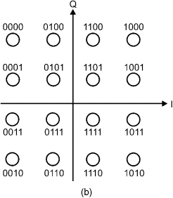
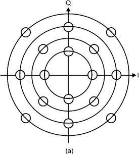
Figure 5.46 Quadrature amplitude modulation: (a) 16QAM-circular and (b) 16QAM-rectangular
As the number of points or distinct states increases, there is an increase in the number of amplitude levels, which does not allow use of high efficiency non-linear amplifiers. Though spectrally very efficient, power output and efficiency suffer due to the requirement to use linear amplifiers. QAM is widely used in TV, Wi-Fi wireless LANs, satellites and cellular telephone systems.
5.7.9 Amplitude Phase Shift Keying (APSK)
As outlined in case of QAM, higher levels of QAM of 16 and above have many amplitude levels and phase shifts. An increased number of amplitude levels makes noise and interference more likely. Amplitude phase shift keying (APSK), which is a combination of amplitude and phase shift keying, is a variant of M-PSK and QAM that incorporates the advantages of both M-PSK and QAM. It has relatively fewer amplitude levels compared to QAM, thus allowing the use of non-linear power amplifiers, and also has relatively greater phase shifts between adjacent phase positions compared to M-PSK. While the former feature produces higher power output and efficiency; latter feature produces a lower bit error rate. Fewer amplitude levels and a smaller difference in amplitude between different levels make it possible to operate in the non-linear region of the power amplifier to boost output power level.
APSK uses fewer amplitude levels. In this case, symbols are arranged into two or more concentric rings with a constant phase shift offset. Figure 5.47 (a) shows the I-Q phase diagram of 16APSK using a double ring PSK format called 4+12 APSK with four symbols in the centre ring and 12 symbols in the outer ring. Figure 5.47 (b) shows the phase diagram of a 32APSK. APSK is primarily used in satellites due to its suitability for use with travelling wave tube (TWT) amplifiers.
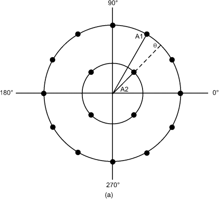

Figure 5.47 Amplitude phase shift keying: (a) 16APSK and (b) 32APSK
5.8 Multiplexing Techniques
Multiplexing techniques are used to combine several message signals into a single composite signal so that they can be transmitted over a common channel. Multiplexing ensures that the different message signals in the composite signal do not interfere with each other and that they can be conveniently separated out at the receiver end. The two basic multiplexing techniques in use include:
- Frequency division multiplexing (FDM)
- Time division multiplexing (TDM)
While frequency division multiplexing is used with signals that employ analogue modulation techniques, time division multiplexing is used with digital modulation techniques where the signals to be transmitted are in the form of a bit stream. The two techniques are briefly described in the following paragraphs.
5.8.1 Frequency Division Multiplexing
In case of frequency division multiplexing (FDM), different message signals are separated from each other in the frequency domain. Figure 5.48 illustrates the concept of FDM showing simultaneous transmission of three message signals over a common communication channel. It is clear from the block schematic arrangement shown that each of the three message signals modulates a different carrier. The most commonly used modulation technique is single side band (SSB) modulation. Any type of modulation can be used as long as it is ensured that the carrier spacing is sufficient to avoid a spectral overlap. On the receiving side, bandpass filters separate out the signals, which are then coherently demodulated as shown. The composite signal formed by combining different message signals after they have modulated their respective carrier signals may be used to modulate another high frequency carrier before it is transmitted over the common link. In that case, these individual carrier signals are known as subcarrier signals.
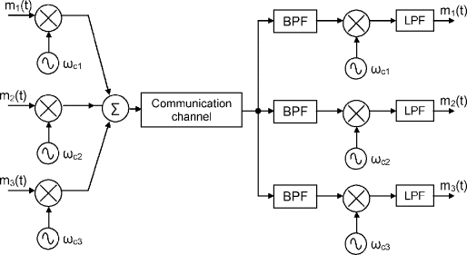
Figure 5.48 Frequency division multiplexing
FDM is used in telephony, commercial radio broadcast (both AM and FM), television broadcast, communication networks and telemetry. In the case of a commercial AM broadcast, the carrier frequencies for different signals are spaced 10 kHz apart. This separation is definitely not adequate if we consider a high fidelity voice signal with a spectral coverage of 50 Hz to 15 kHz. For this reason, AM broadcast stations using adjacent carrier frequencies are usually geographically far apart to minimize interference. In the case of an FM broadcast, the carrier frequencies are spaced apart at 200 kHz or more. In the case of long distance telephony, 600 or more voice channels, each with a spectral band of 200 Hz to 3.2 kHz, can be transmitted over a coaxial or microwave link using SSB modulation and a carrier frequency separation of 4 kHz.
5.8.2 Time Division Multiplexing
Time division multiplexing (TDM) is used for simultaneous transmission of more than one pulsed signal over a common communication channel. Figure 5.49 illustrates the concept. Multiple pulsed signals are fed to a type of electronic switching circuitry, called a commutator in the figure. All the message signals, which have been sampled at least at the Nyquist rate (the sampling is usually done at 1.1 times the Nyquist rate to avoid aliasing problems), are fed to the commutator. The commutator interleaves different samples from different sampled message signals in order to form a composite interleaved signal. This composite signal is then transmitted over the link. In case all message signals have the same bandwidth, one commutation cycle will contain one sample from each of the messages. Where signals have different bandwidths, more samples would need to be transmitted per second of the signals having larger bandwidths. As an illustration, if there are three message signals with respective sampling rates of 2.4 kHz, 2.4 kHz and 4.8 kHz, then each cycle of commutation will have one sample each from the first two messages and two samples from the third message.
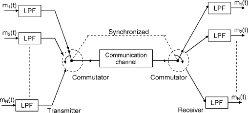
Figure 5.49 Time division multiplexing
At the receiving end, the composite signal is de-multiplexed using a similar electronic switching circuitry that is synchronized with the one used at the transmitter. TDM is widely used in telephony, telemetry, radio broadcasting and data processing applications.
If T is the sampling time interval of the time multiplexed signal of n different signals, each having a sampling interval of Ts, then
Also, if the time multiplexed signal is considered as a lowpass signal having a bandwidth of fTDM and fm is the bandwidth of individual signals, then
5.8.3 Code Division Multiplexing
Code division multiplexing (CDM) allows message signals from multiple independent signal sources to be transmitted simultaneously over a common frequency band. This is unlike either FDM or TDM. In the case of FDM, as discussed in section 5.8.1, multiple message signals are transmitted simultaneously but are separated in frequency domain. In the case of TDM, as discussed in section 5.8.2, multiple message signals are transmitted over a common frequency band and are separated from each other by transmitting them in different time slots. While FDM is used in the case of analogue signals, the latter is applicable to transmission of digital bit streams.
CDM is accomplished by using orthogonal codes called spreading codes, which spread each of the message signals over a common large frequency band, larger than the minimum bandwidth that would otherwise be required to transmit these signals. After different signals are spread over a large common frequency band using one of the spread spectrum techniques, such as direct sequence spread spectrum, they modulate a common carrier and are transmitted over a common channel. At the receiver end, appropriate orthogonal codes are used to recover the corresponding message signals. In other words, at the receiver relevant orthogonal code is used to recover the intended signal from the knowledge of the type of spreading code used for that signal at the transmitter. Figures 5.50 (a) and (b) show the block schematic arrangements used for the direct sequence spread spectrum for spreading and de-spreading operations, respectively, at the transmitter and receiver.
Figure 5.50 Direct sequence spectrum for (a) spreading operation and (b) de-spreading operation
To summarize, the spread spectrum technique of CDM is a three-step process of (a) spreading the bandwidth of each message signal by using a spreading code that is independent of message information, (b) modulating a carrier with the spread spectrum signal and transmitting it over a common transmission channel and (c) using the relevant de-spreading codes at the receivers to recover the intended message signals. Figure 5.51 shows a simplified arrangement of a communication system using CDM. It may be mentioned here that CDM techniques inherently provide reliability, noise immunity and security features to the communication and therefore are extensively used in a number of commercial cellular telephone systems. The technique is used in many contemporary mobile telephone standards including (a) cdmaOne, the first cellular standard to use CDM and implement the code division multiple access (CDMA) scheme and also known as IS-95, (b) CDMA2000, a family of 3G mobile technology standards also known as IMT multi-carrier (IMT-MC) employing CDM and CDMA access to send voice, data and signalling data between mobile phones and cell sites and (c) the universal mobile telecommunications system (UMTS), a 3G mobile cellular system employing wide band code division multiple access (W-CDMA) technology and used for networks based on the GSM standard.
Figure 5.51 Simplified arrangement of communication system using code division multiplexing
Further Readings
- Calcutt, D. and Tetley, L. (1994) Satellite Communications: Principles and Application, Edward Arnold, a member of the Hodder Headline Group, London.
- Elbert, B.R. Introduction to Satellite Communication, Altech House, Boston, Massachusetts.
- Gedney, R.T., Schertler, R. and Gargione, F. (2000) The Advanced Communication Technology, SciTech., New Jersey.
- Kadish, J.E. (2000) Satellite Communications Fundamentals, Artech House, Boston, Massachusetts.
- Kennedy, G. and Davis, B. (1992) Electronic Communication Systems, McGraw-Hill Education Europe.
- Maral, G. and Bousquet, M. (2002) Satellite Communication Systems: Systems, Techniques and Technology, John Wiley & Sons, Ltd, Chichester.
- Richharia, M. (1999) Satellite Communication Systems, Macmillan Press Ltd.
- Stallings, W. (2004) Wireless Communications and Networks, Prentice-Hall, Englewood Cliffs, New Jersey.
- Tomasi, W. (1997) Advanced Electronic Communications Systems, Prentice-Hall, Englewood Cliffs, New Jersey.
- Tomasi, W. (2003) Electronic Communications System: Fundamentals Through Advanced, Prentice-Hall, Englewood Cliffs, New Jersey.
Internet Sites
- http://en.wikipedia.org/wiki/Amplitude_modulation
- http://en.wikipedia.org/wiki/Frequency_modulation
- http://www.rfcafe.com/references/electrical/frequency_modulation.htm
- http://www.tm.agilent.com/data/static/downloads/eng/Notes/interactive/an-150-1/hp-am-fm.pdf
- http://en.wikipedia.org/wiki/Pulse-code_modulation
- http://www2.uic.edu/stud_orgs/prof/pesc/part_3_rev_F.pdf
- http://www.cisco.com/warp/public/788/signalling/waveform_coding.html
- http://www.web-ee.com/primers/files/AN-236.pdf
- http://www.dip.ee.uct.ac.za/~nicolls/lectures/eee482f/04_chancap_2up.pdf
- http://en.wikipedia.org/wiki/Shannon-Hartley_theorem
- http://www.complextoreal.com/chapters/mod1.pdf
- http://users.pandora.be/educypedia/electronics/rfdigmod.htm
- http://www.maxim-ic.com/appnotes.cfm/appnote_number/686
- http://en.wikipedia.org/wiki/QPSK
Glossary
- 16PSK:
- The 16PSK digital modulation technique is an extension of quadrature phase shift keying. It has 16 defined phase changes and each phase change is represented by four bits. It employs 16 symbols with constant amplitude carrier signal and a phase shift of 22.5°
- 8PSK:
- 8PSK digital modulation technique is an extension of quadrature phase shift keying. It has eight defined phase changes and each phase change is represented by three bits. It employs eight symbols with constant amplitude carrier signal and a phase shift of 45°
- A3E system:
- This is the standard AM system used for broadcasting. It uses a double side band with a full carrier
- Adaptive delta modulation:
- This is a type of delta modulator. In delta modulation, the dynamic range of the amplitude of the message signal m(t) is very small due to threshold and overload effects. In adaptive delta modulation, the step size (Δ) is varied according to the level of the message signal. The step size is increased as the slope of the message signal increases to avoid overload. The step size is reduced to reduce the threshold level and hence the quantizing noise is reduced when the message signal slope is small
- Amplitude modulation:
- This is the analogue modulation technique in which the instantaneous amplitude of the modulated signal varies directly as the instantaneous amplitude of the modulating signal. The frequency of the carrier signal remains constant
- Amplitude phase shift keying:
- Amplitude phase shift keying (APSK) is a combination of amplitude and phase shift keying. It is a variant of M-PSK and QAM that incorporates the advantages of M-PSK and QAM
- Amplitude shift keying:
- This is a digital modulation technique. In the simplest form of amplitude shift keying (ASK), the carrier signal is switched ON and OFF depending upon whether a ‘1’ or ‘0’ is to be transmitted. This is also known as ON–OFF keying. In another form of ASK, the amplitude of the carrier is switched between two different amplitudes
- B8E system:
- This system uses two independent side bands with the carrier either attenuated or suppressed. This form of amplitude modulation is also known as independent side band (ISB) transmission and is usually employed for point-to-point radio telephony
- C3F system:
- Vestigial side band (VSB) transmission is the other name for this system. It is used for transmission of video signals in commercial television broadcasting. It is a compromise between SSB and DSB modulation systems in which a vestige or a part of the unwanted side band is also transmitted, usually with a full carrier along with the other side band. The typical bandwidth required to transmit a VSB signal is about 1.25 times that of an SSB signal
- Delta modulation:
- Delta modulation has various forms. In one of the simplest forms, only one bit is transmitted per sample just to indicate whether the amplitude of the current sample is greater or smaller than the amplitude of the immediately preceding sample
- Differential PCM:
- In differential PCM, each word or code group indicates a difference in amplitude (positive or negative) between the current sample and the immediately preceding one
- Differential phase shift keying:
- This is another form of PSK. In this, instead of the instantaneous phase of the modulated signal determining which bit is transmitted, it is the change in phase that carries message intelligence. In this system, one logic level (say ‘1') represents a change in phase of the carrier and the other logic level (i.e. ‘0') represents no change in phase
- Frequency division multiplexing:
- In the case of frequency division multiplexing (FDM), different message signals are separated from each other in frequency. FDM is used in telephony, commercial radio broadcast (both AM and FM), television broadcast, communication networks and telemetry
- Frequency modulation:
- This is the analogue modulation technique in which the instantaneous frequency of the modulated signal varies directly as the instantaneous amplitude of the modulating or base band signal. The rate at which these frequency variations take place is proportional to the modulating frequency
- Frequency shift keying:
- In frequency shift keying (FSK), it is the frequency of the carrier signal that is switched between two values, one representing bit ‘1’ and the other representing bit ‘0’
- H3E system:
- This is the single side band, full carrier AM system
- J3E system:
- This is the single side band suppressed carrier AM system. It is the system usually referred to as SSBSC, in which the carrier is suppressed by at least 45 dB in the transmitter
- Multiple phase shift keying:
- Multiple phase shift keying (M-PSK) modulation techniques such as 8PSK and 16PSK have a larger number of phase positions of the constant amplitude carrier signal, thereby achieving a higher bit rate for a given symbol rate
- Offset QPSK:
- Offset QPSK is similar to QPSK with the difference that the alignment of the odd/even streams is shifted in case of offset QPSK by an offset equal to T seconds, which is the pulse duration of the input bit stream
- Phase shift keying:
- In phase shift keying (PSK), the phase of the carrier is discretely varied with respect to either a reference phase or to the phase of the immediately preceding signal element in accordance with the data being transmitted. For example, when encoding bits, the phase shift could be 0o for encoding a bit ‘0’ and 180° for encoding a bit ‘1'. The phase shift could have been −90° for encoding a bit ‘0’ and +90° for encoding a bit ‘1’
- Pulse amplitude modulation:
- In the case of pulse amplitude modulation (PAM), the signal is sampled at regular intervals and the amplitude of each sample, which is a pulse, is proportional to the amplitude of the modulating signal at the time instant of sampling
- Pulse code modulation:
- In pulse code modulation, the peak-to-peak amplitude range of the modulating signal is divided into a number of standard levels, which in the case of a binary system is an integral power of 2. The amplitude of the signal to be sent at any sampling instant is the nearest standard level. This nearest standard level is then encoded into a group of pulses. The number of pulses (n) used to encode a sample in binary PCM equals log 2 L, where L is the number of standard levels
- Pulse position modulation:
- In the case of pulse position modulation (PPM), the amplitude and width of the sampled pulses are maintained as constant and the position of each pulse with respect to the position of a recurrent reference pulse varies as a function of the instantaneous sampled amplitude of the modulating signal
- Pulse width modulation:
- In the case of pulse width modulation (PWM) the starting time of the sampled pulses and their amplitude is fixed. The width of each pulse is made proportional to the amplitude of the signal at the sampling time instant
- Quadrature amplitude modulation:
- Quadrature amplitude modulation (QAM) is a combination of amplitude and phase shift keying modulation techniques. It makes use of both phase shifts and amplitude variations to increase the bit rate
- Quadrature phase shift keying:
- Quadrature phase shift keying (QPSK) is the most commonly used form of PSK. A QPSK modulator is simply two BPSK modulators operating in quadrature. The input bit stream (d0, d1, d2, d3, d4, ...) representing the message signal is split into two bit streams, one having, say, even numbered bits (d0, d2, d4, ...) and the other having odd numbered bits (d1, d3, d5, ...). The two bit streams modulate the carrier signals, which have a phase difference of 90o between them. The vector sum of the output of two modulators constitutes the QPSK output
- R3E system:
- This is the single side band reduced carrier type AM system, also called the pilot carrier system
- Sampling theorem:
- The sampling theorem states that a band limited signal with the highest frequency component as fM Hz can be recovered completely from a set of samples taken at the rate of fs samples per second provided that fs ≥ 2fM
- Shannon–Hartley theorem:
- The Shannon–Hartley theorem describes the capacity of a noisy channel (assuming that the noise is random). According to this theorem,

- The Shannon–Hartley theorem underlines the fundamental importance of the bandwidth and the signal-to-noise ratio in communication. It also shows that for a given channel capacity, increased bandwidth can be exchanged for decreased signal power
- Time division multiplexing:
- Time division multiplexing is used for simultaneous transmission of more than one pulsed signal over a common communication channel and different message signals are separated from each other in time. TDM is widely used in telephony, telemetry, radio broadcast and data processing