
CHAPTER THREE
DC Performance
3.1 GENERAL STRUCTURES AND STEADY-STATE BEHAVIOR
3.1.1 Electron and Hole Currents
The central design principle of heterostructure devices utilizes energy gap variations in addition to electric fields as forces acting on electrons and holes to control their distribution and flow [1]. By a careful combination of energy gap variations and electric fields, it becomes possible, within wide limits, to control the forces acting on electrons and holes, separately. A design freedom not achievable in homostructures is obtained. The resulting greater design freedom permits a reoptimization of the doping levels and geometries of the HBT, leading to higher-speed devices.
In HBT a wide energy bandgap emitter is used. The basic theory behind a wide-gap emitter is explained as follows. Consider the energy band structure of an N-p-n bipolar transistor (the capital N represents the wide bandgap emitter), as shown in Fig. 3.1. The emitter–base band edge is sufficiently graded to eliminate any band-edge discontinuities in the conduction band. The dc currents flowing in such a transistor include a current In of electrons injected from the emitter into the base, a current Ip of holes injected from the base into the emitter, and a current Is due to electron–hole recombination within the emitter–base space-charge layer. In addition, a small part Ir of the electron injection current In is lost due to bulk recombination. Neglecting recombination effects, the maximum current gain βmax is ≈ Jn/Jp. The electron and hole injection current densities are of the form
where υnb and υpe are the mean speeds, NE and NB are emitter and base doping levels, and q Vn and q Vp are the heights of the potential energy barriers for electrons and holes between the emitter and base. Since the energy gap of the emitter is larger than that of the base, we obtain
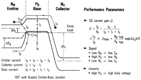
FIGURE 3.1 Current flow of the HBT (after Kroemer, Ref. 1 © IEEE).
As a result of a large energy gap difference between emitter and base, very high values of In / Ip can be achieved regardless of the doping ratio.
3.1.2 Abrupt and Graded Heterojunctions
For an abrupt N-p heterojunction, the conduction energy spike necessitates thermionic emission and tunneling for electron transport from the N-to-p quasineutral regions and the valence-band discontinuity suppresses hole injection from the p-to-N regions. The energy-band diagram of a heterojunction is shown in Fig. 3.2. Because of the valence-band discontinuity that suppresses hole injection into the emitter, the current gain of the heterojunction bipolar transistor has been increased significantly compared to that of the silicon bipolar transistor. The base doping of the HBT is thus increased to maintain a reasonable current gain. The increase in base doping decreases the base resistance.
The dominant transport mechanisms across an abrupt heterojunction are thermionic emission and tunneling. Thermionic emission theory relates barrier height to an injection current in the absence of tunneling. An expression for thermionic-field emitted current derived for Schottky barrier diodes can be written as
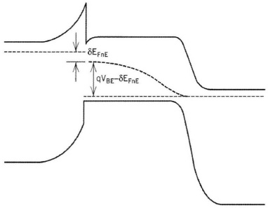
FIGURE 3.1 Energy-band diagram of an abrupt HBT.
where E0 = E00 coth(E00/kT), E00 = (qh/4π)(Ndεqm*)0.5, Φ is the barrier height (from conduction band in bulk to top of spike), and JS is the saturation current.
Compared to pure thermionic emission, tunneling through the conduction-band spike lowers the base—emitter bias needed for a given collector current. Reduced forward bias, in turn, implies larger energy barriers for hole injection into both the bulk and the depletion region of the emitter, which leads to improved injection efficiency. Tunneling through the spike generally serves to raise the ideality factor of the collector current. At low bias, the top of the spike is relatively narrow, and most electrons tunnel relatively far below the nominal peak. With increased forward bias, the top of the spike becomes thicker, and most electrons tunnel at higher energy levels than they do at low bias. Thus the effective barrier height increases with bias, creating an ideality factor greater than 1.
Figure 3.3 shows the measured terminal currents of abrupt AlGaAs/GaAs HBTs in both the forward and reverse active modes from many different wafers fabricated using MOCVD. In this figure the solid lines represent the emitter currents in the reverse active mode. These lines are almost identical for all the wafers measured. This indicates that diffusion is the primary mechanism of the carrier transport across the base–collector homojunction. In contrast, the dashed lines in Fig. 3.3 show different ideality factors, depending on the sample measured. All these dashed curves are different from the solid curves. The dashed curves have ideality factors between 1.11 and 1.18. This indicates that the forward terminal current in an abrupt AlGaAs/GaAs HBT is limited by conduction-band barrier transport mechanisms such as thermionic emission and tunneling.
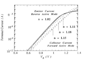
FIGURE 3.3 Measured collector current for forward and reverse active modes of AlGaAs/GaAs HBTs (after Liu et al, Ref. 2 © IEEE).
Current transport mechanisms in GaInP/GaAs HBTs are investigated. To determine the dominant current-transport mechanism in the GaInP/GaAs HBTs, the Gummel plot is displayed. Figure 3.4 illustrates measured terminal currents of the GaInP/GaAs HBT in both the forward active and reverse active modes. The device has an emitter area of 100 × 100 μm2, and its base–collector junction area is about 110 × 200 μm2. When the device is in the forward active mode, conduction carriers are emitted from the emitter–base junction, which is a GaInP/GaAs heterojunction. When the HBT is in the reverse active mode, the conduction carriers are emitted from the base–collector junction, which is a GaAs homojunction. Despite the operation differences in the forward active and reverse active modes, this figure demonstrates that the two terminal currents are nearly identical, with an ideality factor of 1.02. This indicates that carriers injected from both the GaInP/GaAs heterojunction and the GaAs homojunction are limited by the transport across the base layer, not by the conduction barrier. Note that the conduction-band discontinuity of the GaInP/GaAs HBT observed in [2] is much smaller than that of the AlGaAs/GaAs HBT.
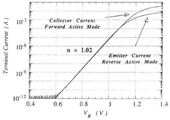
FIGURE 3.4 Measured collector current for forward and reverse active modes of GaInP/GaAs HBTs (after Liu et al, Ref. 2 © IEEE).
The carrier injection efficiency can be improved if a thin region adjacent to the heterojunction is graded, especially for GaAs HBTs. Usually, a grading distance on the order of 100 to 300 Å, related to the Debye length, is sufficient to remove the discontinuity. The Debye length is related to the screening length and hence to the electrostatic field. The heterojunction grading effectively removes the spike and thus makes the thermionic and tunneling mechanisms less important. A linearly graded heterojunction with complete removal of the energy-band spike and discontinuity, shown in Fig. 3.5, has transport behavior similar to that of a homojunction.
For an abrupt heterojunction, the electron current density across the heterointerface is the difference between two opposing fluxes [3]:

FIGURE 3.5 Energy-band diagram of a graded emitter–base heterojunction.
where ![]() and
and ![]() are the electron concentrations at each side of the heterointerface and υn is the mean electron thermal velocity. These concentrations may be related to the electron concentrations at the boundaries of the space-charge region:
are the electron concentrations at each side of the heterointerface and υn is the mean electron thermal velocity. These concentrations may be related to the electron concentrations at the boundaries of the space-charge region:
and
where VBE is the base–emitter voltage, εE the permittivity in the emitter, and εB the permittivity in the base.
The electron current density given by (3.5) should be equal to the electron current density due to diffusion at the boundary of the space-charge region in the base:
where Dn is the electron diffusion constant, Ln the electron diffusion, and WB the base thickness. Equating (3.5) and (3.8), one can solve for n(X1) and then Jn(X1).
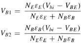
Figure 3.6 shows the collector current density versus the base–emitter voltage of the AlGaAs/GaAs HBT for various graded layer thicknesses (Wg = 0 for an abrupt heterojunction). The collector current density increases considerably when the graded layer thickness is increased from 0 to 150 Å. The collector current density increases only slightly when Wg is increased from 150 Å to 300 Å. Note that the roll-off of JC at high VBE for both Wg = 150 Å and 300 Å is due to the presence of the “alloy” barrier in the graded layer.
3.1.3 Undoped Setback Layer
Another approach to improve the injection efficiency is to insert a thin intrinsic spacer or setback layer at the heterojunction. The setback layer reduces the impurity out-diffusion from the heavily doped region and alters the potential barrier of the heterojunction for improving the injection efficiency. Figure 3.7 shows the energy-band diagram of an abrupt AlGaAs/GaAs HBT with an undoped setback layer. The effective potential barrier for electrons injected from emitter to base is reduced significantly. The reduction of the electron potential barrier, in turn, increases the electron injection into the base. Note that the addition of the spacer layer increases not only the injected current across the heterojunction, but also the recombination at the heterojunction space-charge region.
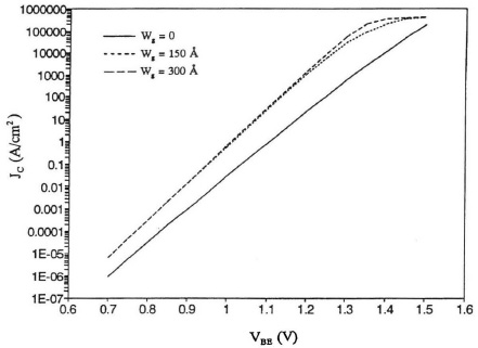
FIGURE 3.6 JC−VBE characteristics (after Liou, Ref. 4 © Artech House).
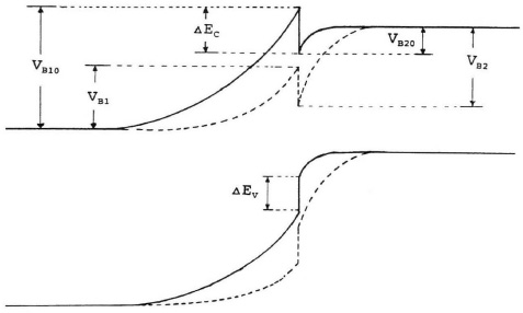
FIGURE 3.7 Energy-band diagram of an HBT with a setback layer.

FIGURE 3.8 Effect of setback layer thickness on the collector current of an HBT (after Liou et al., Ref. 5 © Elsevier Science).
The effect of setback layer thickness (Wi) on the collector current density of an AlGaAs/GaAs HBT is shown in Fig. 3.8. In the JC−VBE characteristics, the lines represent the analytical predictions and the symbols represent the numerical simulation results. Clearly, the setback layer improves the emitter injection efficiency, particularly when the base–emitter voltage is relatively low. Also note that there is a smaller increase in collector current density when the setback layer thickness is increased from 100 Å to 200 Å than from 0 to 100 Å.
3.1.4 Graded-Base HBTs
With the ability to control semiconductor bandgap, it is also worthwhile to establish a gradual change in bandage across the base layer from EG0 near the emitter to EG0 − ΔEG near the collector. In such a situation, the high hole conductivity ensures that the valence band is effectively flat, and the bandgap shifts establish a conduction-band energy gradient equal to ΔEG/WB. This energy gradient constitutes a quasi-electric field that drives electrons across the base by drift as well as diffusion.
Figure 3.9 shows the energy-band diagram of a graded-base HBT. An aiding builtin field EB is formed in the quasi-neutral base which results in a reduction in the minority-carrier transit time and an increase in the common-emitter current gain. EB can be obtained by varying the Al or Ge mole fraction in the base, which varies the electron affinity χ and thus the conduction-band edge in the base. The magnitude of the aiding field is determined by the difference of the electron affinity at the collector–base space-charge layer edge and at the emitter-base space-charge-layer edge in the base divided by the base width.
FIGURE 3.9 Energy-band diagram of a graded-base HBT.
A change of bandgap using a linear grading at small mole fractions gives
Since the intrinsic carrier concentration varies exponentially with the bandgap, the position-dependent intrinsic carrier concentration is written as
where ni0 is the intrinsic carrier concentration associated with the bandgap EG0 at the emitter edge of the quasi-neutral base. The corresponding quantities at the collector edge are ![]() and EG1. The current density of a graded heterojunction bipolar transistor with a linearly graded, uniformly doped base is given by [6]
and EG1. The current density of a graded heterojunction bipolar transistor with a linearly graded, uniformly doped base is given by [6]

3.1.5 Double Heterojunctions
Another possibility offered by bandgap engineering is to increase the bandgap of the collector. These types of devices are referred to as double heterojunction bipolar transistors (DHBTs). A wide bandgap collector suppresses the injection of holes from the base into the collector when the base–collector junction becomes forward biased. Increasing the bandgap of the collector greatly diminishes the charge storage in saturation and speeds up device turn-off from the saturation region. With double-heterojunction devices, symmetrical operation in the upward and downward directions can be established, which leads to circuit flexibility. Additional advantages of wide-bandgap collector devices are the increase in breakdown voltage and the reduction in leakage current.
The energy-band diagram of a double-heterojunction bipolar transistor is shown in Fig. 3.10. Note that the influence of the spike in the emitter–base heterojunction highlights a larger ideality factor on the corresponding current component, whereas the influence of the collector–base junction spike is characterized only by a saturation current. In an HBT with a heterojunction collector, an alloy barrier effect [7] also appears. The alloy barrier effect in the collector is essentially the same as in the emitter. At low currents, the alloy potential difference appears in the valence band, resulting in the usual hole-retarding barrier and field, while at higher currents it appears partially in the conduction band as a barrier to the flow of minority carriers. The consequences of this barrier are excess charge storage in the base and a decrease of current gain resulting from recombination.
Figure 3. 11 shows two perspective plots of the conduction-band edge energy in the base of a double-heterojunction bipolar transistor at VBE = 1.3 and 1.5 V, with zero base–collector bias VBC = 0 V. The region plotted extends 500 Å into both the emitter and the collector. The 1.3-V surface is shifted down for clarity. The emitter junction is located in the lower right, and the collector is the broader region in the background. The base is the constant-energy region. Both heterojunctions are parabolically graded. At low bias, the potential profile is similar to that of a homojunction bipolar transistor. At higher voltages, however, a barrier due to both the alloy potential and electron space charge appears at the collector junction [8,9]. This barrier is largest where the current density is largest (i.e., opposite the emitter injection). The barrier is lower in the extrinsic part of the HBT because the current density is lower there. Significant spreading of the electron current goes toward the extrinsic base because the alloy barrier varies proportionally with current density.

FIGURE 3.10 Energy-band diagram of a double-heterojunction bipolar transistor.
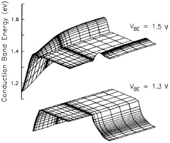
FIGURE 3.11 Conduction-band diagram at VBE = 1.3 and 1.5 V (after Tiwari et al., Ref. 8 © IEEE).
Current gain behavior for single-heterojunction, graded-base, and double-heterojunction bipolar transistors in the absence of surface recombination (s = 0 cm/s) [8] is shown in Fig. 3.12. Similar behavior at a surface velocity of 2 × 10⁵ and 2 × 106 cm/s is also observed. The graded base has larger current gains than those of single- and double-heterojunction bipolar transistors over a wide range of collector current densities. The larger current gain in the graded-base HBT is due to the aiding quasi-electric field, which reduces the storage of electrons in the base and hence the neutral base recombination. The double-heterojunction HBT shows a rapid drop at high collector current densities due to the base–collector barrier effect. Although the graded-base HBT has a lower barrier-to-hole injection into the emitter, its gain actually continues to be comparable to that of the other devices at low current densities.
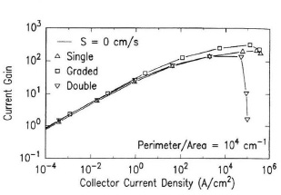
FIGURE 3.12 Current gain versus collector current in the absence of surface recombination (after Tiwari and Frank, Ref. 9 © IEEE).
3.1.6 Electron Quasi-Fermi Level Splitting
In the abrupt heterojunction, a forward-biased junction reduces the barrier to electron flow into the base, yet increases the barrier to electron flow in the opposite direction. This leads to a situation where the net electron flow in the heterojunction space-charge region may not be small compared to each of the counter-direct flows. The flow of electrons thus cannot be considered as a perturbation from equilibrium. It was first proposed by Perlman and Feucht [10] that the electron quasi-Fermi level be discontinuous at the metallurgical boundary of an abrupt heterojunction. Lundstrom quantified the electron quasi-Fermi level splitting by using boundary conditions for the electron concentration on the p-side of the junction. These were arrived at by equating the thermionic emission current across the junction to the diffusion current away from the junction. The degree of electron quasi-Fermi level splitting was presented by Pulfrey and Searles [11].
The electron quasi-Fermi level splitting is given by
where n(0) is the excess electron concentration at the base edge of the emitter–base space-charge region and nb0 is the electron concentration in the base at equilibrium. Note that ΔEC and ΔEV result from the formation of a heterojunction. ΔEFn is obtained due to electron current flow across the forward-biased heterojunction. ΔEC and ΔEV are physical constants, and ΔEFn is a function of bias.
Figure 3.13 shows the electron quasi-Fermi level splitting versus base–emitter voltage. For the abrupt heterojunction with tunneling included, the electron quasi-Fermi level splitting rises steadily with base–emitter voltage. This is because ΔEFn increases with forward bias, which leads to a reduction in the back injection of electrons and in increasing departure from quasiequilibrium. Suppression of the conduction-band spike by junction grading gives the barrier a more homojunction-like character. Thus electron quasi-Fermi level splitting is greatly reduced. By neglecting tunneling, the current at the junction is underestimated. This exaggerates the restrictive role of the junction as regards charge transport and leads to an overestimation of the electron quasi-Fermi level splitting.
The electron Fermi level splitting for both single- and double-heterojunction bipolar transistors with uniform and graded bases is shown in Fig. 3.14. For low base–emitter voltages, the DHBT virtually eliminates collector–emitter offset voltage. At VBE = 1.5 V the electron quasi-Fermi level splitting is reduced to less than 50 meV for the DHBT with a uniform base, while it is about 170 meV for the SHBT. Grading the base reduces the amount of electron quasi-Fermi level splitting in an SHBT but increases it in a DHBT, although the degree of splitting is inherently less in a DHBT than in a SHBT. In the SHBT, the most important manifestation of base grading is the reduction in the conduction-band spike. This makes the junction more homojunction-like, so the electron quasi-Fermi level splitting is reduced. Interestingly, although this effect is also present in the DHBT case, it is swamped by the effect of the built-in base field, which sweeps carriers away from the emitter–base junction. This action opposes that of the electron barrier at the base–collector junction. Thus n(0) is not augmented to the same degree as it is in the uniform-base case, the departure from quasiequilibrium increases and therefore the electron quasi-Fermi level splitting increases.

FIGURE 3.13 Electron quasi-Fermi level separation (after Pulfrey and Searles, Ref. 11 © IEEE).

FIGURE 3.14 Electron quasi-Fermi level separation (after Pulfrey and Searles, Ref. 11 © IEEE).
3.1.7 Collector–Emitter Offset Voltage
AlGaAs/GaAs single-heterojunction bipolar transistors exhibit significant collector–emitter offset voltage ΔVCE, as evidenced by experimental data [12] in Fig. 3.15. This offset voltage reduces logic swing in digital circuits and increases power dissipation in analog amplifiers. The offset voltage arises because the base–emitter and base–collector junctions are very dissimilar in their current–voltage dependence. For example, the built-in voltage for electrons in the base–emitter heterojunction is larger than that in the base–collector homojunction. It may also arise because devices have a large combination current that is dependent on area and lifetime. Widely different areas for the base–emitter and the base–collector junctions can therefore give rise to large offsets because of asymmetric junction areas.
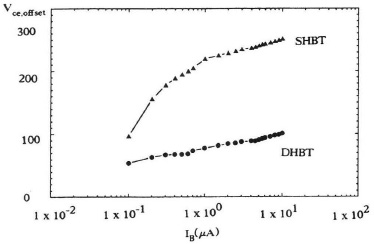
FIGURE 3.15 Offset voltage versus base current (after Won et al., Ref. 12 © IEEE).
Examine the collector current using the Ebers–Moll equation as follows:
where αN is the normal common-base current gain, αN IE0 = α1 IC0, where α1 is the inverse common-base current gain. The offset voltage can be deduced by setting IC = 0 in (3.13):
Although the offset voltage of InAlAs/InGaAs HBTs is slightly less than that of AlGaAs/GaAs HBTs, the offset voltages were found to originate from the asymmetry of emitter and collector junctions [12, 13]. Figure 3.16 shows variation of the offset voltage with the collector–emitter ratio (AE/AC) at a base current of 1 μA. The offset voltage is sensitive to AC / AE The offset voltage can be lowered by increasing the injection of electrons from the collector in the offset region and decreasing AC / AE The closer the inverse current transfer factor α1 is to unity, the smaller is the offset voltage. In fact, negligible offset voltage is observed when the transistor is operated in the inverted mode as shown in Fig. 3.17. In this case the appropriate offset voltage is the emitter-to-collector offset voltage, and the contribution of the first and second terms in (3.13) is negative. Thus one of the advantages of employing the collector-up structure can be the negligible offset voltage in the common-emitter configuration. For a single AlGaAs/GaAs heterojunction bipolar transistor, the collector-to-emitter offset voltage can be as large as 200 to 300 m V. This offset voltage is reduced significantly when double heterojunctions are used. Grading of the base–emitter heterojunction also reduces the offset voltage [14].

FIGURE 3.16 Offset voltage with collector–emitter area ratio (after Won et al., Ref. 12 © IEEE).

FIGURE 3.17 Collector current at the inverse active mode (after Won et al., Ref. 12 © IEEE).
The offset voltage is also a function of temperature. Figure 3.18 shows the collector current versus the collector–emitter voltage of an AlGaAs/GaAs HBT grown by chemical vapor deposition at 300, 423, 573, and 623 K. The HBT shows a low collector–emitter offset voltage of 0.1 V at 300 K. The offset voltage is increased to 0.4 V at 573 K. At higher temperatures, significant collector–base leakage current starts to degrade transistor performance. The ideality factors obtained from the Gummel plot are shown in Fig. 3.19. At 300 K the collector current exhibits an ideality factor of nC = 1.04, indicating diffusion-dominated current transport. The ideal behavior is maintained until it starts to increase at 523 K. The ideality factor nB of the base current at 300 K is 1.97, which is close to the ideal value of 2 for a pure recombination current. At temperatures higher than 523 K, the ideality factor of nB increases to 3.
3.1.8 Early Voltage
The Early voltage (VA) is an important parameter for the bipolar transistor. It describes the base-width modulation effect of the BJT in the forward-active mode. Since the discovery of the Early effect in 1952 [16], numerous papers on Early voltage have been published [17–20]. Roulston [17] studied mathematically the Early voltage of narrow-base bipolar transistors, including the effect of velocity saturation in the collector–base junction. Velocity saturation increases the effective Early voltage of the bipolar transistor. A more self-consistent equation was derived by Liou [18]. Yuan and Liou [19] reported that the Early voltage is influenced by both the base–emitter voltage and the collector–base voltage of the BJT. This effect is significant for modern bipolar transistors with very narrow base width WB. Ugajin et al. [20] investigated the inverse base width modulation effect when the bipolar transistor is operated at high current densities before base pushout occurs. Unlike the Early voltage effect, the inverse base width modulation increases base width and hence decreases the collector current.

FIGURE 3.18 Collector current versus collector–emitter voltage at (a) 300 K, (b) 423 K, (c) 573 K, and (d) 623 K (after Fricke et al., Ref. 15 © IEEE).

FIGURE 3.19 Ideality factors for base and collector currents versus temperature (after Fricke et al., Ref. 15 © IEEE).
The definition of the Early voltage is given by
where VCE is the collector–emitter bias. For an HBT with high base doping, the Early voltage is relatively large. Grading in the base of the HBT also increases the Early voltage.
3.1.9 Bias-Dependent Base Resistance
The base resistance plays a significant role in the switching speed of bipolar logic and the frequency response of small-signal amplifiers. The base resistance can be divided by the intrinsic base resistance Rbi and the extrinsic base resistance Rbx. The intrinsic base resistance for a double-base contact bipolar transistor is given by
where XE is the emitter width in the horizontal dimension and WB is base thickness in the vertical dimension. WB is subject to base width modulation, base conductivity modulation, emitter current crowding, and base pushout effects. This makes the base resistance current dependent [21].
The base width is modulated by the moving edge of the emitter–base space-charge region when VBE changes. As VBE increases, the emitter–base space-charge region contracts, and WB expands. This reduces Rbi because the base cross-sectional area WBLE increases, resulting in a larger base charge and a larger effective Gummel number.
When an n-p-n bipolar transistor is in high current operation, the hole concentration (including the excess carrier concentration) in the base will exceed the acceptor (dopant) concentration to maintain charge neutrality. As a result, the base sheet resistance under the emitter decreases as the hole injection level increases. The intrinsic base resistance is then decreased as the level of injection increases.
The nonuniform emitter current density distribution makes the effective emitter width smaller. Hence emitter current crowding reduces the effective intrinsic base resistance. For a bipolar transistor with a large emitter width at high base–emitter voltage, Rbi is more susceptible to emitter crowding effect.
For bipolar transistors operating at high currents, base pushout occurs. The base pushout increases the effective base width, which decreases the intrinsic base resistance. For a bipolar transistor with low epi-layer collector doping operating at high collector current density and low VCE, the intrinsic base resistance is more vulnerable to the base pushout effect.
Figure 3.20 shows the base resistance versus the base current of a heterojunction bipolar transistor. The base resistance was obtained from the Gummel plot measurement. It is clear from Fig. 3.20 that the base resistance decreases with increase in base current. It is anticipated that the base current dependence will be enhanced if a lower base doping is used.
3.1.10 High Injection Barrier Effect
Heterojunction bipolar transistors rely on a difference in bandgap to obtain a selective suppression of carriers from the base into the emitter. Double-heterojunction bipolar transistors such as SiGe HBTs exhibit a unique effect at high current densities. As the collector current is larger than the onset current for base pushout, holes tend to move into the lightly doped collector when the electric field at the collector–base junction changes from negative to positive. The valence-band discontinuity at the base–collector heterojunction, however, prevents holes from moving into the collector. Thus electrons in the collector are not compensated with holes, and an electric field is established that creates a potential barrier [23]. This barrier opposes the electron flow into the collector, and an increased density at the base–collector heterojunction is required to support the collector current density.

FIGURE 3.20 Base resistance versus base current (after Lu et al., Ref. 22 © IEEE).
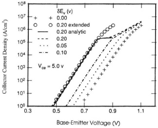
FIGURE 3.21 High current IC versus VBE (after Cottrell and Yu., Ref. 23 © IEEE).
Figure 3.21 shows the collector current density versus base–emitter voltage. The n-p-n SiGe HBT with uniform base and collector doping and varying valence band offset magnitude in the base. The base has a constant valence-band offset except for the case labeled “extended,” where the narrow bandgap region is extended through the collector to the buried layer. The base width is 0.25 μm and the collector doping is 1 × 1016 cm−3. The transistor structure was chosen to emphasize and isolate this effect rather than to represent a “real” design. The solid line in Fig. 3.21 represents results obtained with the analytic model and the remainder with SEDAN [24]. It is clear from Fig. 3.21 that the collector current density decreases significantly at high base-emitter voltages due to the high-injection barrier effect.
The high current barrier effect has also been shown in the AlGaAs/GaAs/ AlGaAs HBT [8]. Figure 3.22 illustrates the Gummel plot of this double-heterojunction HBT for the emitter area 4 × 12μm2. The HBT has a base doping of 5 × 1018cm−3 and thickness of 100 Å, an emitter doping of 4 × 1017cm−3, a collector doping of 1 × 1017cm−3, and an aluminum mole fraction of 0.3. In Fig. 3.22 the base current shows a rapid rise at high current densities, with the point of rapid increase dependent on the applied base–collector voltage. The onset of this effect is pushed toward higher current densities or base–emitter voltages with increased reverse biasing of the base–collector junction. The barrier decreases the electron injection into the collector and leads to large electron accumulation or hole recombination in the base. This is why the collector current is decreased and the base current is increased at high base–emitter voltages.
Consider a base–collector heterojunction with a parabolically graded GaAs/AlGaAs junction. Under low injection conditions, the alloy grading results in a retarding chemical field for holes from the base and none for electrons because most of the alloy grading potential appears in the valence band. As injection increases, the decreasing net charge density in the depletion region, and hence reduced electrostatic field, leads to the appearance of some of this potential as an electron chemical barrier that retards the flow of electrons also. An electron barrier just begins to appear when the electrostatic field is the same as the electron chemical field resulting from alloy grading.
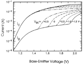
FIGURE 3.22 High current IC versus VBE (after Tiwari, Ref. 7 © IEEE).
Figure 3.23 shows the conduction-band edge and quasi-Fermi level for electrons at the base–collector junction for base–emitter voltages of 1.3, 1.4, and 1.5 V and VBC = 0 V. At high collector current densities, the mobile charge concentration becomes sufficiently large, resulting in the appearance of the bandgap grading–related electron chemical potential barrier. This barrier is about 0.07 eV at a forward voltage of 1.5 V at the base–emitter junction, corresponding to an emitter current density of 8 × 10⁴ A/cm2. The electron barrier is seen to form after the forward bias of 1.3 V and increases with forward biasing of the emitter–base junction. When a reverse bias is applied at the base–collector junction, the barrier is reduced because of an increase in the compensating electrostatic field, thus reducing the magnitude of this effect.

FIGURE 3.23 Conduction-band edge and electron quasi-Fermi level at VBE = 1.3, 1.4, and 15 V (after Tiwari, Ref. 7 © IEEE).
The degradation of collector current due to the conduction-band barrier effect may be related to the following degradation factor [23]:
where
![]()
EM is the electric field at the base–collector metallurgical junction, εC the permittivity in the collector, NC the collector doping, and υS the saturation velocity. The agreement between the analytic and device simulation in [23] seems to justify the simplifying assumptions and lends credibility to the physical explanation of this high-injection barrier phenomenon.
Joseph et al. [25] used a one-dimensional device simulator to examine the barrier effect of the SiGe HBT with a triangle Ge profile in the base. Electric field as a function of position in the base and collector at JC = 0.1 and 4.0 mA/μm2 is shown in Fig. 3.24. The collector–base voltage is equal to 0 V. The ambient temperature is at 200 K. As seen in Fig. 3.24, the electric field at JC = 4 mA/μm2 shows a bump at the base–collector heterojunction (≈ 260 nm from emitter contact). The conduction-band edge in the base and collector at JC = 0.1, 2.0, and 4.0 mA/μm2 is displayed in Fig.3.25. It is clear from this figure that a conduction barrier has been formed at a current density of 4 mA/μm2.

FIGURE 3.24 Electric field versus position to demonstrate the collector–base heterojunction barrier effect (after Joseph et al., Ref. 25 © IEEE).

FIGURE 3.25 Simulated conduction-band edge of an SiGe HBT (after Joseph et al., Ref. 25 © IEEE).
3.2 SiGe HETEROJUNCTION BIPOLAR TRANSISTORS
The SiGe bipolar transistor in the BiCMOS process is attractive for low-cost, mixed-signal wireless applications, due to its high performance and process compatibility with Si technology. In this section, some unique features of the SiGe HBT not discussed in Section 3.1 are presented.
3.2.1 Current Gain and Early Voltage Product
The germanium profiles with the same total germanium content and graded-base width include uniform, trapezoid, and triangle profiles, as shown in Fig. 3.26. The grading of the Ge across the quasi-neutral base induces a drift field in the base which accelerates the electrons injected from the emitter to the collector, thereby decreasing the base transit time compared to a Si BJT. Figure 3.27 shows the SiGe/Si ratio for the three parameters of current gain, Early voltage, and gain–Early voltage product [26]. The x-axis represents the total Ge grading across the base. At ΔEg,Ge(grade) = 0, a pure Ge box profile of 8.4% Ge is obtained, while at ΔEg,Ge(grade) = 125 meV, a purely triangular profile of 0 to 18.6% Ge is obtained. The intermediate Ge trapezoid is located between these two extremes. The triangular profile has the largest Early voltage and gain–Early voltage product. The box profile, however, has the highest current gain since the enhancement of current gain depends exponentially on the boundary value in bandgap reduction at the emitter–base junction.
The advantages of the SiGe HBT can also be analyzed by the equations as follows. The collector current density of an n-p-n HBT where the bandgap can vary across the base is given by


FIGURE 3.26 Uniform, triangle, and trapezoid Ge profiles in the base of an SiGe HBT.
For the SiGe bipolar transistor with a trapezoid Ge profile, the intrinsic carrier concentration in the base is given by

where ΔEg,Ge(0) is the bandgap reduction due to Ge concentration at x = 0, ΔEg,Ge(WB) the bandgap reduction due to Ge concentration at x = WB, ![]() the apparent bandgap narrowing due to heavy doping effect in the base, and XT the transition point between the linear and flat Ge concentrations in the base. ΔEg,Ge(grade) = ΔEg,Ge(WB) − ΔEg,Ge(0). For XT = 0 the Ge base profile becomes uniform; for XT = WB, the Ge profile is linear.
the apparent bandgap narrowing due to heavy doping effect in the base, and XT the transition point between the linear and flat Ge concentrations in the base. ΔEg,Ge(grade) = ΔEg,Ge(WB) − ΔEg,Ge(0). For XT = 0 the Ge base profile becomes uniform; for XT = WB, the Ge profile is linear.
Equation (3.18) is valid for the HBT without a conduction-band spike at the emitter–base heterojunction and when the base is at low level of injection. If the base current is caused only by hole injection from base into emitter, JB = JB0 exp(q VBE/kT), the maximum current gain at a moderate base–emitter bias is equal to

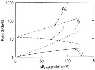
FIGURE 3.27 Early voltage and gain–Early voltage products (after Harame et al, Ref. 26 © IEEE).
where JB0 is the hole diffusion current density into the emitter at zero base–emitter bias. Examining Eq. (3.20), it is clear that the current gain of the SiGe HBT is larger than that of the Si BJT because of a smaller bandgap and a larger intrinsic carrier concentration in the SiGe base. Rewriting the Early voltage in (3.15) gives
The change of base width with respect to collector–base voltage is
where CJC is the collector–base junction capacitance.
The change of collector current density with respect to base width is derived as
Inserting Eqs. (3.22) and (3.23) into (3.21) gives
From Eqs. (3.20) and (3.24) the current gain and Early voltage product is given simply by
It is clear from (3.25) that the βVA product is a strong function of Ge concentration at the edge of the collector–base space-charge layer in the quasi-neutral base form ![]() . It is also clear that the current gain–Early voltage product of the SiGe HBT is larger than that of the Si BJT, due to a larger
. It is also clear that the current gain–Early voltage product of the SiGe HBT is larger than that of the Si BJT, due to a larger ![]() value in the SiGe base.
value in the SiGe base.
Table 3.1 shows measured and calculated values of βVA, JB0 and CJC for four devices with different Ge concentrations in the base. All devices have identical emitter and collector layers. The base consists of two 200-Å-thick SiGe layers with constant Ge profile. On both sides of the base, 40-Å-thick intrinsic SiGe spacer layers were inserted to remove spike-and-notch or conduction-band discontinuity. Using no adjustable parameters, the calculated results using (3.25) are in good agreement with the experimental data. The Early voltage is increased dramatically when the bandgap at the collector edge of the base is lower than the maximum bandgap in the base. A αVA product of over 100,000 for device 3 with 14% Ge at the emitter side and 25% at the collector side in the base has been observed.
3.2.2 Temperature-Dependent Current Gain
Silicon bipolar transistors are generally not considered for operation at liquid-nitrogen temperatures (LNT) because of insufficient current gain [28]. The reduction in current gain is a result of the smaller bandgap in the emitter than in the base. The base current is typically limited by hole injection into the emitter, and its temperature dependence is determined largely by the effective bandgap of the emitter, which is reduced because of a combination of heavy doping effects. The collector current, on the other hand, consists of electrons traversing the base, and its temperature dependence is therefore determined by the bandgap in the base. The difference in bandgap between the emitter and the base causes the current gain to decrease exponentially with temperature by two to three orders of magnitude between room temperature (RT) and liquid-nitrogen temperature. In addition to the drop in current gain, the base resistivity increases sharply because of carrier freeze-out. This effective reduction in base doping provides relatively more collector current but also increases current crowding, which is expected to degrade switching performance.
TABLE 3.1 Measured β, VA, JB0, and RB with Various Ge Concentrations

Recent advances in high-quality low-temperature epitaxial processes offer great potential for achieving the very thin, heavily doped, and abrupt base profiles required for continued vertical scaling of bipolar transistors. Because of the use of smaller bandgap and graded germanium content in the base region, the current gain of the SiGe heterojunction bipolar transistor is superior to that of Si bipolar transistors.
Proper bipolar transistor scaling and design reduce the current gain sensitivity to temperature. Figure 3.28 shows the transistor current gain as a function of reciprocal temperature for bipolar technologies of varying age. In the legend, I/I stands for ion implantation, DD stands for double diffusion, and LTE stands for low-temperature epitaxy. The SiGe technology produces a current gain at LNT which is essentially unchanged from its RT value. The high current gain at low temperature is a result of both the heavily doped base and the presence of SiGe, which offsets the bandgap narrowing in the emitter. These results suggest that silicon–germanium bipolar technology is suitable for very high speed applications at cryogenic temperatures.
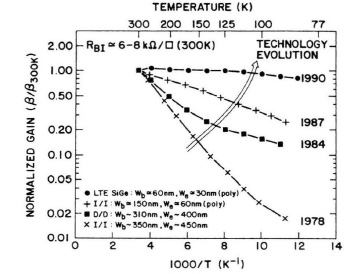
FIGURE 3.28 Current gain versus temperature for different process technologies (after Cressler et al., Ref. 29 © IEEE).
3.2.3 Current Gain Roll-off in Graded SiGe Base
For Si homojunction bipolar transistors, the current gain at a moderate injection level is relatively independent of base–emitter bias and collector current [30]. For SiGe heterojunction bipolar transistors with graded bases, however, the current gain exhibits a significant emitter–base bias dependence at moderate VBE [31]. The nonideal collector current is caused by the interaction of the bias dependence of the emitter–base space-charge region width and the exponential dependence of the collector current on the Ge concentration at the edge of the emitter–base space-charge region. For example, the saturation collector current density in a graded-base HBT with a uniformly-doped base is
The saturation current is an exponential function of ΔEg,Ge(0). The location of x = 0, however, is moving with respect to the emitter–base bias. Base-width modulation effect at the emitter–base junction changes the location of the emjtter–base space-charge-layer edge in the base region. For increasing VBE, the emitter–base space-charge layer shrinks. This results in a smaller ΔEg,Ge(0) value for a linearly graded Ge base, as indicated in Fig. 3.29. The exponential dependence of the collector current on this bandgap reduction leads to a significant decrease in the collector current density, even for a minor variation of the width of the emitter–base space-charge region. The normalized current gain versus collector current density at 300 and 85 K is displayed in Fig. 3.30. The normalized current gain decreases with JC due to the base-width modulation effect at the emitter–base junction. The decrease in current gain is faster when Ge grading is increased. This effect is much more pronounced at low temperatures because JC0 is exponentially dependent on the ratio of ΔEg,Ge(0) to kT.
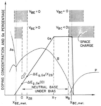
FIGURE 3.29 Schematic of the emitter–base space-charge region and its bias dependence (after Crabbé et al., Ref. 31 © IEEE).
3.2.4 Early Voltage, Including Recombination in the SiGe Base
The Early voltage predicted in (3.24) does not account for the effect of neutral-base recombination (NBR). For the heterojunction bipolar transistor with a heavily doped base, the neutral-base recombination is significant. Analytical equations to examine the output conductance of silicon bipolar transistors with large neutral-base recombination current were derived by McGregor et al. [32]. Neutral-base recombination increases the output conductance at a given collector current. A similar analytical study was published by Mohammandi and Selvakumar [33].
We now present the Early voltage of SiGe bipolar transistors with neutral-base recombination in the base. Using (3.21), the derivative of JC with respect to WB is given by


FIGURE 3.30 Normalized current gain versus collector current density (after Crabbé et al., Ref. 31 © IEEE).
Neglecting emitter–base space-charge-layer recombination, the total base current density is written
where JB0 is the preexponential base current density for hole injection into the emitter and τ is the position-dependent electron lifetime in the base. The first term in Eq. (3.28) represents the recombination current in the emitter and the second term represents the recombination in the base. At constant JB, dVBE/dJB could be set to zero. The derivative of (3.28) gives
Using Leibniz’s rule for the differentiation of integrals yields
Since n(WB) is negligible at the forward active mode, (3.30) can be rewritten
Using
and solving (3.31) gives

where
Substituting Eq. (3.33) into (3.27) leads to

Inserting (3.22) and (3.35) into (3.21) gives [34]
The effect of neutral-base recombination on the Early voltage of SiGe bipolar transistors can be evaluated by the recombination factor defined as follows:
If the recombination current in the emitter is much larger than that of the base, τ → ∞ and fR → 1. If the recombination current in the base is much larger than that of the emitter, JB0 ≈ 0. For the bipolar transistor with a trapezoid Ge concentration (including linear profile also) in the uniformly doped base, (3.37) reduces to

where A = ΔEg,Ge(grade) / kT.
Figure 3.31 shows the effect of XT / WB on the Early voltage of a SiGe bipolar transistor normalized to that of the Si bipolar transistor. In this plot the solid lines represent the analytical model in (3.36) and the empty squares represent the predictions using [35]. Good agreement between the analytical predictions using (3.36) and in [35] has been obtained. Note that the results in [35] only account for linear Ge grading in the base (i.e., XT / WB = 1), without neutral-base recombination. It is clear from Fig. 3.31 that increasing XT / WB enhances the normalized Early voltage. The normalized Early voltage is plotted against ΔEg,Ge(grade) / kT in Fig. 3.32. The empty squares represent the linear Ge concentration in the base. As shown in Fig. 3.32, the larger the Ge grading, the larger the normalized Early voltage. The increasing rate is nearly exponential. The normalized Early voltage for a flat Ge profile (XT / WB = 0) is independent of ΔEg,Ge(grade) / kT, which is consistent with device physics.

FIGURE 3.31 Normalized Early voltage versus XT / WB.
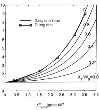
FIGURE 3.32 Normalized Early voltage versus ΔEg,Ge(grade) / kT.
As indicated in [32,33], neutral-base recombination current changes the Early voltage and output conductance of bipolar transistors. The normalized Early voltage versus ΔEg,Ge(grade) / kT between two extreme conditions (0 and 100% neutral-base recombination) is shown in Fig. 3.33. In this figure the dashed line represents the HBT without neutral-base recombination, the dotted line represents the device with 100% neutral-base recombination (i.e., no recombination in the emitter), the solid line represents the model predictions with both neutral-base recombination and back injection into the emitter, and the solid circles represent the experimental data [27]. In this plot, the SiGe HBTs have two stepped flat Ge profiles with positive and negative ΑEg,Ge(grade) / kT. The agreement between the analytical predictions using (3.36) and experimental data is very good. The analytical predictions without taking into account neutral-base recombination are overestimated. The predictions taking into account 100% neutral-base recombination (or no back injection into the emitter) give the normalized Early voltage of 0.5, independent of the Ge grading.
The recombination factor fR in (3.38) for the Early voltage versus XT / WB is displayed in Fig. 3.34. At XT / WB = 0, the recombination factor is 0.5. This is identical to that published in [32] for a silicon bipolar transistor without Ge content in the base. When both Ge grading [i.e., ΑEg,Ge(grade) / kT] and XT / WB increase, the recombination factor decreases significantly. This indicates that the neutral-base recombination current must be considered in evaluation of the Early voltage when Ge grading is increased. This plot also demonstrates that a fast degradation occurs for XT / WB from 0 to about 0.4. The degradation is more significant for larger Ge grading.
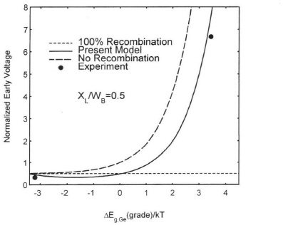
FIGURE 3.33 Normalized Early voltage versus ΔEg,Ge(grade) / kT (with and without neutral-base recombination).

FIGURE 3.34 Recombination factor for the Early voltage versus XT / WB for various ΔEg,Ge(grade) / kT values.
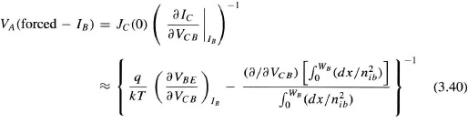
It is clear that base bandgap and temperature significantly affect the βVA product of transistors in the presence of neutral-base recombination. Figures 3.35 and 3.36 show the typical common-emitter output characteristics (IC − VCE) for a SiGe HBT obtained using forced IB and forced VBE at 358 and 200 K, respectively. In a forced-IB situation, VBE is allowed to change in such a way as to maintain constant IB. Due to the fact that IB decreases with increasing VCB in the presence of neutral-base recombination, VBE is forced to increase so as to maintain a constant IB. The analytical equation of VA under forced-VBE conditions is given by
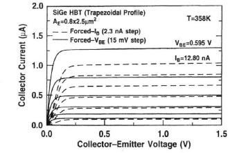
FIGURE 3.35 Collector current versus collector–emitter voltage under forced VBE and IB conditions at 358 K (after Joseph et al., Ref. 36 © IEEE).

FIGURE 3.36 Collector current versus collector–emitter voltage under forced VBE and IB conditions at 200 K (after Joseph et al., Ref. 36 © IEEE).

In a forced-VBE situation, VBE is kept constant. The increase of IC is due to the decrease in base width for an increase of VCB. The Early voltage under forced-IB conditions is approximated as
It is apparent from Figs. 3.35 and 3.36 that with cooling, the slope of IC with respect to VCE increases in forced-IB measurement, as opposed to a decrease in the same quantity for a forced-VBE measurement. Figure 3.37 displays VA obtained for both Si and SiGe transistors using forced-IB and forced-VBE conditions as a function of reciprocal temperature. The exponential degradation of VA measured using a forced-IB technique in the trapezoidal-base SiGe HBT is due to the thermally activated nature of the neutral-base recombination of IB through ΔEg,Ge(x = 0).

FIGURE 3.37 Early voltage versus inverse temperature (after Joseph et al., Ref. 36 © IEEE).
Precision current sources (CSs), which are used extensively in many analog circuits, rely on the Early voltage of a transistor to maintain constant current output for large output voltage swings, and thus require large output resistance. Due to the significant differences between the VA of a SiGe HBT, depending on how the device is biased at the input, it is expected that the presence of neutral-base recombination will have a strong impact on the temperature characteristics of such SiGe HBT current sources. Figure 3.38 shows the cascode and Wilson current sources used in high-precision analog circuits. The impact of NBR on the temperature characteristics of these circuits has been examined using SPICE. The temperature dependence of NBR was modeled by introducing a collector-to-base resistance whose values were determined experimentally from the inverse slope of the IB versus VCB characteristics. Figure 3.39 shows the close agreement between the modified SPICE model predictions and the measured common-emitter output characteristics for the SiGe HBT at 358 and 200 K, respectively. The output resistance of cascode and Wilson current sources versus temperature predicted by SPICE simulation with and without NBR is shown in Fig. 3.40. Under the ideal situation (i.e., without NBR), both current sources show an increase in the output resistance with cooling. In the presence of NBR in the transistors, however, the output resistance of both current sources is not only smaller compared to the ideal case but also has the opposite temperature dependence.
3.2.5 Inverse Base Width Modulation Effect
Base pushout is the usual mechanism underlying the high current degradation of bipolar transistors. At high current densities, mobile carriers modulate the collector–base junction space charge and push it into the epitaxial collector. The effective quasi-neutral base widens. For SiGe bipolar transistors with high collector doping concentration, base pushout effect is reduced. Two physical mechanisms, inverse base width modulation and collector space-charge-region widening, become important before base pushout. Inverse base width modulation is a widening of the quasi-neutral base width. The collector–base space-charge-region layer on the base side shrinks as the collector current density increases. Mobile carriers modulate the space charge and diminish the electric field at the junction. The inverse base width modulation decreases the current gain and increases the base transit time of the HBT [20].
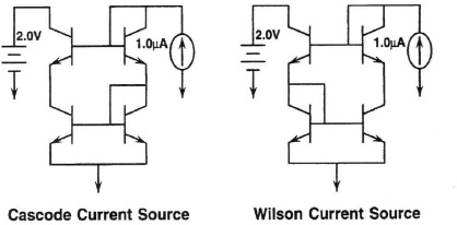
FIGURE 3.38 Cascade and Wilson current sources.
The base widening due to inverse base width modulation and collector space-charge-layer widening is illustrated in Fig 3.41. The magnitude of the peak electric field in the collector–base space-charge region diminishes with increasing collector current density because of current-induced perturbation and ohmic drops in the collector region. This causes the collector–base space-charge-layer thickness on the base side to decrease and hence the quasi-neutral base width to increase. The inverse base width modulation begins at a collector current density below the onset current density for base pushout.
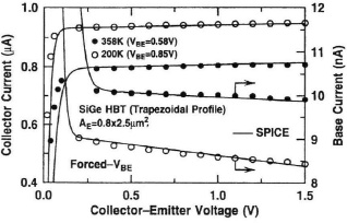
FIGURE 3.39 Collector current versus collector–emitter voltage (SPICE prediction versus experiment) (after Joseph et al., Ref. 36 © IEEE).

FIGURE 3.40 Output resistance versus temperature (after Joseph et al., Ref. 36 © IEEE).
Assuming that the base doping profile is exponential, the thicknesses of WSC and WSCC are given by [20]
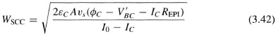
where NC = NA0 exp(−η), REPI is the epitaxial collector resistance, I0 = q AυsNEPI, and ![]() = VBC + ICRC − IBRB.
= VBC + ICRC − IBRB.

FIGURE 3.41 Bipolar doping profile for demonstrating inverse base width modulation effect (after Ugain et al., Ref. 20 © IEEE).
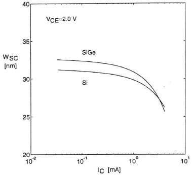
FIGURE 3.42 WSC versus IC (after Ugajin et al., Ref. 20 © IEEE).
Figure 3.42 shows the dependence of WSC on the collector current with and without Ge incorporation. The two transistors have an effective emitter area of 0.2 × 3.0μm2. Although the low-IC values of WSC differ between the two devices (because of slight differences in base doping near the collector junction), both devices show significant decrease in WSC at IC ≈ 2 mA. This result supports the significance of inverse base width modulation at high collector currents in highly scaled transistors.
3.3 III/V COMPOUND HETEROJUNCTION BIPOLAR TRANSISTORS
In this section we address some unique de characteristics of III/V compound HBTs not presented in Section 3.1.
3.3.1 Self-Heating Effect
Heterojunction bipolar transistors using GaAs semi-insulating substrates exhibit self-heating effects due to low thermal conductivity of the GaAs semi-insulating substrate (about one-third of Si thermal conductivity) [37]. The collector current of the heterojunction bipolar transistor shows a negative differential resistance at high power dissipation levels, as seen in Fig. 3.43. Unlike the silicon bipolar transistor, which has a positive temperature coefficient for current gain, the heterojunction bipolar transistor exhibits a decrease in current gain with increasing collector–base voltage due to self-heating. The negative temperature coefficient of the current gain results from bandgap narrowing in the base of the HBT. For example, self-heating causes the increase in base and collector currents. The increase in base current is larger than that of the collector current. Thus, for a constant base current in the IC−VCE plot, the collector current decreases with increasing collector–emitter voltage. The negative resistance effect becomes significant when the power dissipation is large. Therefore, reducing the self-heating effect is very important for power heterojunction bipolar transistor circuit design.
FIGURE 3.43 Collector current versus collector–emitter voltage to demonstrate self-heating effect.
Self-heating could change analog circuit response significantly. For example, consider the current mirror in Fig. 3.44, with two discrete heterojunction bipolar transistors Q1 and Q2 and two external resistors R1 and R2. Since the collector–emitter voltage of Q1 equals the base–emitter voltage VBE1, the bipolar transistor Q1 usually does not experience self-heating. However, the collector–emitter voltage of the bipolar transistor Q2 is VCC − IC2R2 and the bipolar transistor Q2 can have significant self-heating if the collector current QC2 and the collector–emitter voltage of Q2 are high. Self-heating of Q2 can thus result in a totally different output current, which is much higher than the designed current at the isothermal condition. For a fixed resistor R1, for instance, the collector current IC1 of the reference transistor Q1 is constant. The collector current IC2 of transistor Q2 follows the reference current IC1 when R1 = R2. If the resistance of R2 is decreased, the collector current IC2 will increase due to the increase of collector–emitter voltage at Q2. The output current IC2 will then be much larger than the reference current.
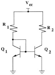
FIGURE 3.44 Schematic of a current mirror.
Figure 3.45 shows the sensitivity of the collector currents for reference transistor Q1 and mirror transistor Q2 as a function of 1 / R2 at VCC = 15 V. The resistor R1 is selected at 2 kΩ in order to make the base–emitter voltage VBE equal to 1.4 V. The mirror current designed to operate at the isothermal condition should follow the reference current (solid line in Fig. 3.45). The predicted mirror current with self-heating, however, increases with decreasing R1 due to an increase in the collector–emitter voltage for Q2. The solid squares of Fig. 3.45 represent R1 simulated at 2 kΩ, 1.5 kΩ, 1 kΩ, 500 Ω, 333 Ω and 250 Ω, respectively. The corresponding relative error (IC2 − IC1)/IC1 is 4.85, 17.3, 31, 46, 51.3, and 54.1%, respectively.
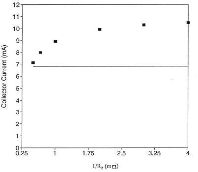
FIGURE 3.45 Collector current versus 1 / R2 (after Yuan, Ref. 38 © IEEE).
Since the size of the intrinsic HBT (e.g., intrinsic emitter, base, and collector) is much smaller than that of the extrinsic HBT (e.g., subcollector and semi-insulating substrate), the temperature in the intrinsic HBT can be considered spatially independent. Heat generated in the intrinsic HBT is dissipated primarily through an effective heat diffusion area in the semi-insulating substrate. The heat power PS generated in the HBT is thus
The temperature increment due to self-heating is related to power dissipation and thermal resistance Rth:
where T is the lattice temperature and T0 is the ambient temperature (300 K). Note that the heat is dissipated throughout the semi-insulating substrate with a lateral diffusion angle θ [39] as shown in Fig. 3.46, and the thermal conductivity of GaAs is proportional to (T / T0)−b. This, together with the Kirchhoff transformation [40],

FIGURE 3.46 Heat diffusion of an HBT throughout the semi-insulating substrate (after Liou et al., Ref. 39 © IEEE)
where
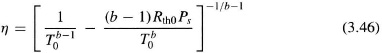
Here Rth0 is the thermal resistance for the case that the thermal conductivity in the semi-insulating substrate is temperature independent and Rth is the temperature-dependent thermal resistance.
For microwave HBTs, the multiemitter finger structure is frequently used. Such a structure allows less power to be generated in each HBT unit cell, thus making the self-heating effect less prominent than to its single-emitter finger counterpart. The thermal effect in the multiemitter HBT is more complicated than that in the single-emitter finger HBT, because thermal coupling among the neighboring fingers is also important in the multiemitter finger HBT. The combination of self-heating and thermal coupling is examined in detail in Chapter 7. Note that InAlAs/InGaAs HBTs on InP substrates have a relatively smaller self-heating effect because of the higher substrate thermal conductivity of InP substrates (0.7 versus 0.46 W cm−1 K−1). A list of thermal conductivities for key semiconductor materials is given in Table 3.2.
The self-heating effect in III/V HBTs could be enhanced in high-temperature operation. The dc performance of a single-emitter finger HBT operating at high ambient temperature (between 300 and 500 K) has been investigated [41]. Both large (100 × 100μm2)- and small (2 × 10μm2)-emitter-area HBTs were considered. The self-heating effect of the large-emitter-area HBT is less significant than that of the small emitter area HBT because the large emitter area allows heat generation to be dissipated quickly.
TABLE 3.2 Thermal Conductivity of Elemental and Compound Semiconductors
| Semiconductor | κ(W cm−1K−1) |
|---|---|
| Si | 1.5 |
| Ge | 0.6 |
| AlP | 0.9 |
| AlAs | 0.8 |
| AlSb | 0.57 |
| GaAs | 0.46 |
| GaP | 0.77 |
| GaSb | 0.39 |
| InAs | 0.273 |
| InP | 0.68 |
| InSb | 0.166 |
3.3.2 Recombination Currents
The major sources of generation–recombination effects in the heterojunction bipolar transistors are the emitter–base and collector–base space-charge regions, the quasi-neutral base and emitter, the surface at the extrinsic base, and the surface at the junction depletion region edges. The emitter quasi-neutral recombination can be ignored in most cases because hole injection is suppressed efficiently by the valence-band discontinuity ΔEV. The recombination in the collector–base space-charge region is not important because the junction is reverse biased under normal operating conditions. Figure 3.47 shows the relative recombination rates of recombination in the space-charge region and at the surface compared to quasi-neutral recombination. This figure shows that the electrons injected into the base recombine copiously at the surface of the GaAs base and at the base–emitter junction and that holes injected from the base recombine at the GaAlAs emitter surface. Of these, the base surface and the base–emitter space-charge recombination are the dominant components. The quasi-neutral base recombination is the smallest.
The space-charge recombination in the base–emitter junction has a 2kT exponential dependence. Surface recombination at the extrinsic base behaves similar to bulk recombination in the quasi-neutral base. Surface recombination at the junction depletion region edges behaves similarly to conventional recombination in the depletion region. Tiwari and Frank [9] have analyzed the surface recombination numerically using the single acceptor–donor model. At low currents, the surface recombination current density follows a 1.8kT behavior. At high currents and high surface recombination velocity, the ideality factor shows a 1.2kT dependence. The effective way of separating these “surface” recombination mechanisms from the “bulk” recombination mechanisms is to observe the device size dependence of base current and current gain.

FIGURE 3.47 Relative recombination rates of a heterojunction bipolar transistor (after Tiwari and Frank, Ref. 9 © IEEE).
The semiconductor surface is characterized by a surface recombination velocity and a surface-state density. Compared to InP HBTs with GaAs counterparts, InGaAs lattice matched to InP substrates have a smaller surface recombination velocity than that of GaAs (103 cm/s versus 106 cm/s). Therefore, the surface recombination current of InP HBTs should be much smaller. For AlGaAs/GaAs HBTs, however, the extrinsic base surface recombination can be a major component of the overall base current. Surface recombination can be minimized by various technologies, including the use of surface chemical passivation or the use of a wide-gap material at the surface of the extrinsic base. This could be a p-type GaAlAs obtained by converting the polarity of the injection emitter, or a depleted GaAlAs emitter region (by thinning of this material). The use of a graded-base layer may also reduce the surface recombination.
The extrinsic base surface passivated with a thin depleted AlGaAs layer virtually eliminates the surface recombination current and increases the current gain of AlGaAs/GaAs HBTs. Experimental results [42] of passivated and unpassivated AlGaAs/GaAs HBTs of various emitter areas are compared here. The HBTs have a linearly graded emitter-base heterojunction with a AlGaAs grading layer of 300 Å. In smaller devices, the emitter width WE is varied from 4, 8, 12, to 16 μm, and the emitter length LE is 10 μm. For bigger devices, the emitter area is 100 × 100 μm2. The relation between the current gain and the emitter dimensions is given by
where JBB, JBSCR, and JBE are the recombination current densities in the base, emitter–base space-charge region, and emitter. KBsurf is the surface recombination current divided by the emitter periphery.
Figure 3.48 shows measured JB (= JC / β versus (1 / WE + 1 / LE) for passivated and unpassivated HBTs at JC = 104 A/cm2. The intercept of the curves with the y-axis represents the sum of JBB, JBSCR, and JBE. The slope represents 2KBsurf. It is clear from this plot that the unpassivated HBTs have significant KBsurf. The passivated HBTs show virtually no variation with (1 / WE + 1 / LE), demonstrating that the surface recombination current in the passivated devices is indeed negligible. Figure 3.49 shows measured Gummel plots for HBTs with emitter areas of 4 × 10 and 12 × 10 μm2. The ideality factors of collector currents are about 1, indicating that the collector current is diffusion limited in the base layer. This is because the emitter–base heterojunction has a linearly graded AlGaAs layer. More important, Fig. 3.49 shows that the ideality factors for the base currents are 1.71 for the passivated device and 1.33 for the unpassivated device with emitter area of 4 × 10 μm2. For the passivated and unpassivated devices with an emitter area of 12 ×10 μm2, the ideality factors are 1.76 and 1.49, respectively. For passivated devices, the surface recombination is negligible.

FIGURE 3.48 Measured JC(1 / β) versus (1 / WE + 1 / LE) (after Liu and Harris, Ref. 42 © IEEE).
The overall base recombination current dominates by space-charge recombination. This is why the ideality factor is close to 2. For unpassivated devices, the overall base current is the sum of the space-charge region recombination and the surface recombination. The ideality factors in this case indicate that the surface recombination current increases with the base–emitter voltage with an ideality factor of between 1 and 1.33. Figure 3.50 shows the current gain versus collector current. The HBTs in this plot have a linearly graded base-emitter heterojunction. The emitter area of the devices is 4 × 10 μm2. As demonstrated in Fig. 3.50, the current gain of passivated devices improves significantly.
3.3.3 Temperature-Dependent Current Gain of AlGaAs/GaAs HBTs
GaAs has a wide bandgap which suppresses the thermal generation of carriers and thus reduces leakage currents more effectively than does silicon. Microwave devices with an extended temperature range for space applications may be realized because of GaAs’s high electron mobility and saturation velocity. High-temperature operational amplifiers with excellent frequency response may be realized using AlGaAs/GaAs HBTs.
Figure 3.51 displays the small-signal current gain hFE, β, and IC as a function of temperature. The current gain is defined by
![]()

FIGURE 3.49 Gummel plot of an HBT (after Liu and Harris, Ref. 42 © IEEE).
At increased temperatures, hFE, β, and IC are reduced by the same order of magnitude. The increase in current gain at the highest temperature measured (523 K) is due to the additional hole leakage current from the collector into the emitter.
An analytical description that highlights the important physical parameters influencing the temperature dependence of the current gain in heterojunction bipolar transistors has been developed [43]. Each of the possible base current components was discussed and its relative importance to temperature dependence was assessed. For a typical abrupt AlGaAs/GaAs HBT, the current gain versus collector current at various temperatures was simulated, and the result is shown in Fig. 3.52a. The collector and base current were computed self-consistently using generalized Ebers–Moll transport equations taking into account thermal effects and electrical effects, including tunneling through the conduction-band spike, electron quasi-Fermi level splitting, base bandgap narrowing, and series resistances in the emitter and collector. The space-charge-region recombination currents are evaluated numerically using Shockley–Read–Hall statistics.

FIGURE 3.50 Current gain versus collector current (after Liu and Harris, Ref. 42 © IEEE).
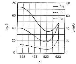
FIGURE 3.51 Dependence of hFE, β, and IC on temperature (after Fricke et al., Ref. 15 © IEEE).
The dominance of the large variations with temperature of SCR recombination at low currents is shown clearly in Fig. 3.52a. The current gain versus temperature for a 200-Å graded AlGaAs/GaAs HBT is also shown (Fig. 3.52b). Similar temperature dependence of current gain for the AlGaAs/GaAs HBT measured at different substrate temperatures is shown in Fig. 3.53.
In abrupt HBTs, the ΔEC/ΔEV partitioning ratio determines the relative importance of reverse hole current compared to injected electron current. The conduction-band discontinuity ΔEC suppresses the electron current, causing an increase in the relative importance of the reverse hole current. Tunneling significantly enhances the current gain at low currents, but its role at high currents is less effective because of the flattening of the conduction-band spike. At high temperatures, the thermionic emission component of the electron current becomes more important. Also, the reverse hole injection could be significant as the temperature is raised.
In general, the following temperature-dependent characteristics have been observed [43]:
- The gain of HBTs in the base–emitter bias region is governed by SCR recombination in the emitter and is subject to large reductions with increasing temperature despite the fact that the recombination lifetime is generally thought to increase with temperature.
FIGURE 3.52 Calculated current gain versus collector current at different temperatures for (a) an abrupt AlGaAs/GaAs HBT and (b) a linearly graded AlGaAs/GaAs HBT (after Ng et al., Ref. 43 © IEEE).
- Extrinsic base surface recombination in GaAs is unlikely to cause significant temperature dependence of current gain even in unpassivated structures, where it can dominate the base current.
- At high current densities, reverse hole injection can contribute to limiting the gain and may be the main cause of negative differential resistance (NDR) in abrupt AlGaAs/GaAs HBTs, where the conduction-band discontinuity is large.
- At very high base doping (> 2 × 1019 cm−3), in devices whose gain is limited by base bulk recombination, the negative temperature dependence of the dominate Auger recombination lifetime in GaAs can result in NDR.


FIGURE 3.53 Measured cunent gains versus collector current of AlGaAs/GaAs HBTs at various temperatures (after Liu et al., Ref. 44 © IEEE).
3.3.4 Temperature-Dependent Current Gain of InP-Based HBTs
AlInAs/GaInAs heterojunction bipolar transistors grown on InP substrate have gained considerable attention for high-performance, low-power, and low-voltage applications. These devices have demonstrated excellent reliability and stable device characteristics under high-temperature stress. AlInAs/GaInAs HBT technology is also attractive for cryogenic applications because of the narrow bandgap of the GaInAs base layer, which leads to a low turn-on voltage for the device.
An AlInAs/GaInAs HBT on the InP substrate grown by MBE was studied [45]. The base–emitter turn-on voltage was measured from −196 to 250°C. The base–emitter turn-on voltage is 0.64 V at JC = 5 × 10³ A/cm2. The low turn-on voltage of this HBT is due to the use of the low bandgap GaInAs base. The temperature coefficient of the turn-on voltage is approximately −0.95 mV/°C. The current gain over the temperature range from −196 to 250°C is relatively stable, as shown in Fig. 3.54. The dc current gain is measured from a 2 × 5μm2 HBT at VBC = 0 V and JC = 5 × 10³ 5 × 10⁴, and 2.5 × 10⁵ A/cm2. From room temperature up to 250°C, the current gain is decreased by 15%. From room temperature to liquid-nitrogen temperature (−196°C), the current gain is increased by 5% at JC = 2.5 × 10⁵ A/cm2.
Similar temperature behavior has been observed in AlxGa0.52−x In0.48P/GaAs HBTs grown by MOCVD [46]. Nearly-ideal de characteristics observed at room temperature are maintained up to at least T = 623 K across the entire range of aluminum composition x. The excellent quality of the emitter for direct bandgap compositions means that the current gain is limited by the base bulk recombination current, giving rise to temperature-insensitive current gain performance and a lack of negative differential resistance.
Figure 3.55 shows a plot of current gain versus collector current from 300 to 623 K for the AlxGa0.52−x In0.48P/GaAs HBTs with two different Al composition values (x = 0.18 and 0.52). The current gain decreases substantially only at low currents and only after the temperature has risen to more than 500 K, while at higher currents the gain is stable with both collector current and temperature. The larger bandgap emitter device (S5) demonstrates a greater range of current gain stability at low currents.

FIGURE 3.54 Current gain versus temperature of an AlInAs/GaInAs HBT (after Hafizi et al., Ref. 45 © IEEE).
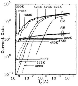
FIGURE 3.55 Temperature-dependent current gain characteristics of AlxGa0.52−x In0.48P/GaAs HBTs with x = 0.18 (S2) and x = 0.52 (S5) (after Yow et al., Ref. 46 © IEEE).
REFERENCES
1. H. Kroemer, “Theory of wide-gap emitter for transistor,” Proc. IRE, 45, 1535 (1957).
2. W. Liu, S.-K. Fan, T. S. Kim, E. A. Beam III, and D. B. Davito, “Current transport mechanism in GaInP/GaAs heterojunction bipolar transistors,” IEEE Trans. Electron Devices, ED-40, 1378 (1993).
3. M. Shur, GaAs Devices and Circuits, Plenum, New York (1987).
4. J. J. Liou, Principles and Analysis of AlGaAs/GaAs Heterojunction Bipolar Transistors, Artech House, Norwood, MA (1996).
5. J. J. Liou, C. S. Ho, L. L. Liou, and C. I. Huang, “An analytical model for current transport in AlGaAs/GaAs abrupt HBTs with a setback layer,” Solid-State Electron., 36, 819 (1993).
6. H. Kroemer, “Heterostructure bipolar transistors and integrated circuits,” Proc. IEEE, 70, 13 (1982).
7. S. Tiwari, “A new effect at high currents in heterostructure bipolar transistors,” IEEE Electron Device Lett., EDL-6, 142 (1988).
8. S. Tiwari, S. L. Wright, and A. W. Kleinsasser, “Transport and related properties of (Ga,Al)As/GaAs double heterostructure bipolar junction transistors,” IEEE Trans. Electron Devices, ED-34, 185 (1987).
9. S. Tiwari and D. J. Frank, “Analysis of the operation of GaAlAs/GaAs HBTs,” IEEE Trans. Electron Devices, ED-36, 2105 (1989).
10. S. S. Perlman and D. L. Feucht, “P-n heterojunction,” Solid-State Electron., 27, 911 (1964).
11. D. L. Pulfrey and S. Searles, “Electron quasi-Fermi level splitting at the base–emitter junction of AlGaAs/GaAs HBTs,” IEEE Trans. Electron Devices, ED-40, 1183 (1993).
12. T. Won, S. Iyer, S. Agarwala, and H. Markç, “Collector offset voltage of heterojunction bipolar transistors grown by molecular beam epitaxy,” IEEE Electron Device Lett., EDL-10, 274 (1989).
13. S.-C. Lee, J.-N. Kau, and H.-H. Lin, “Origin of high offset voltage in an AlGaAs/GaAs heterojunction bipolar transistor,” Appl. Phys. Lett., 45(10), 1114 (1984).
14. N. Chand, R. Fisher, and H. Markç, “Collector–emitter offset voltage in AlGaAs/GaAs heterojunction bipolar transistors,” Appl. Phys. Lett., 47(3), 313(1985).
15. K. Fricke, H. L. Hartnagel, W.-E. Lee, and J. Würfl, “AlGaAs/GaAs HBT for high-temperature applications,” IEEE Trans. Electron Devices, ED-39, 1977 (1992).
16. J. M. Early, “Effects of space-charge layer widening in junction transistors,” Proc. IRE, 40, 1401 (1952).
17. D. J. Roulston, “Early voltage in very-narrow-base bipolar transistors,” IEEE Electron Device Lett., EDL-11, 88 (1990).
18. J. J. Liou, “Comments on ‘Early voltage in very-narrow-base bipolar transistors,’” IEEE Electron Device Lett., EDL-11, 236 (1990).
19. J. S. Yuan and J. J. Liou, “An improved Early voltage model for advanced bipolar transistors,” IEEE Trans. Electron Devices, ED-38, 179 (1991).
20. M. Ugajin, G.-B. Hong, and J. G. Fossum, “Inverse base-width modulation and collector space-charge-region widening: degradation effects at high current densities in highly scaled BJTs (and HBTs),” IEEE Trans. Electron Devices, ED-41, 266 (1994).
21. J. S. Yuan, J. S. Yuan, and W. R. Eisenstadt, “Physics-based current-dependent base resistance mode for advanced bipolar transistors,” IEEE Trans. Electron Devices, ED-35, 1055 (1988).
22. K. Lu, A. Perry, and T. J. Brazil, “A new large-signal AlGaAs/GaAs HBT model including self-heating effects, with corresponding parameter-extraction procedure,” IEEE Trans. Microwave Theory Tech., MTT-43, 1433 (1995).
23. P. E. Cottrell and Z. Yu, “Velocity saturation in the collector of Si/Gex,Si1−x/Si HBTs,” IEEE Electron Device Lett., EDL-11, 431 (1990).
24. SEDAN: One-Dimensional Device Analysis Program, Technology Modeling Associates, Inc. Palo Alto, CA, 1984.
25. A. J. Joseph, J. D. Cressler, D. M. Richey, and D. L. Harame, “Impact of profile scaling on high-injection barrier effects in advanced UHV/CVD SiGe HBTs,” IEDM Tech. Dig., 253 (1996).
26. D. L. Harame, J. H. Comfort, J.D. Cressler, E. F. Crabbé, J. Y.-C. Sun, B. S. Meyerson, and T. Tice, “Si/SiGe epitaxial-base transistors: I. Materials, physics, and circuits,” IEEE Trans. Electron Devices, ED-42, 455 (1995).
27. E. J. Prinz and J. C. Sturm, “Current-gain–Early voltage products in heterojunction bipolar transistors with nonuniform base bandgaps,– IEEE Trans. Electron Devices, ED-12, 661 (1991).
28. W. P. Dumke, “The effect of base doping on the performance of Si bipolar transistors at low temperatures,” IEEE Trans. Electron Devices, ED-28, 494 (1981).
29. J. D. Cressler, J. H. Comfort, E. F. Crabbé, G. L. Patton, J. M. C. Stork, J. Y.-C. Sun, and B. S. Meyerson, “On the profile design and optimization of epitaxial Si- and SiGe-base bipolar technology for 77 K applications: I. Transistor de design considerations,” IEEE Trans. Electron Devices ED-40, 525 (1993).
30. S. M. Sze, Physics of Semiconductor Devices, 2nd ed., Wiley, New York (1981).
31. E. F. Crabbé, J. D. Cressler, G. L. Patton, J. M. C. Stork, J. H. Comfort, and J. Y.-C. Sun, “Current gain rolloff in graded-base SiGe heterojunction bipolar transistors,” IEEE Electron Device Lett., EDL-14, 193 (1993).
32. J. M. McGregor, D. J. Roulston, J. P. Noel, and D. C. Houghton, “Output conductance of bipolar transistors with large neutral-base recombination current,” IEEE Trans. Electron Devices, ED-39, 2569 (1992).
33. S. Mohammandi and C. R. Selvakumar, “Analysis of BJT’s, pseudo-HBT’s, and HBT’s by including the effect of neutral base recombination,” IEEE Trans. Electron Devices, ED-41, 1708 (1994).
34. J. Song and J. S. Yuan, unpublished data.
35. W. R. Zhang, W. G. Wu, Z. Zeng, and J. S. Luo, “Effect of Ge composition linear grading in the base on the Early voltage of Si/Si1-xGex/Si HBTs,” Solid-State Electron., 38, 1842 (1995).
36. A. J. Joseph, J. D. Cressler, D. M. Richey, R. C. Jaeger, and D. L. Harame, “Neutral base recombination and its influence on the temperature dependence of Early voltage and current gain–Early voltage product in UHV/CVD SiGe heterojunction bipolar transistors,” IEEE Trans. Electron Devices, ED-44, 404 (1997).
37. D. P. Maycock, “Thermal conductivity of silicon, germanium, III-V compound and III-V alloys,” Solid-State Electron., 10, 161 (1967).
38. J. S. Yuan, “Thermal and reverse base current effects on heterojunction bipolar transistors and circuits,” IEEE Trans. Electron Devices, ED-43, 789 (1995).
39. J. J. Liou, L. L. Liou, C. I. Huang, and B. Bayraktaroglu, “A physics-base heterojunction bipolar transistor including thermal and high-current effects,” IEEE Trans. Electron Devices, ED-40, 1570 (1993).
40. W. B. Joyce, “Thermal resistance of heat sink with temperature-dependent conductivity,” Solid-State Electron., 18, 321 (1975).
41. S.-F. Lin, “Modeling the AlGaAs/GaAs heterojunction bipolar transistor operating in the temperature range of 300 and 500 K,” M.S. thesis, University of Central Florida (1995).
42. W. Liu and J. S. Harris, Jr., “Diode ideality factor for surface recombination current in AlGaAs/GaAs heterojunction bipolar transistors,” IEEE Trans. Electron Devices, ED-39, 2726 (1992).
43. C.-M. S. Ng, P. A. Houston, and H.-K. Yow, “Analysis of the temperature dependence of current gain in heterojunction bipolar transistors,” IEEE Trans. Electron Devices, ED-44, 17 (1997).
44. W. Liu, S.-K. Fan, T. Henderson, and D. Davito, “Temperature dependencies of current gains in GaInP/GaAs and AlGaAs/GaAs heterojunction bipolar transistors,” IEEE Trans. Electron Devices, ED-40, 1351 (1993).
45. M. Hafizi, W. E. Stanchina, R. A. Metzger, P. A. Macdonald, and F. Williams, Jr., “Temperature dependence of dc and RF characteristics of AlInAs/GaInAs HBTs,” IEEE Trans. Electron Devices, ED-40, 1583 (1993).
46. H.-K. Yow, P. A. Houston, C.-M. Ng, C. Button, and J. S. Roberts, “High-temperature dc characteristics of AlxGa0.52−x In0.48P/GaAs heterojunction bipolar transistors grown by metal organic vapor phase epitaxy,” IEEE Trans. Electron Devices, ED-43, 2 (1996).
PROBLEMS
3.1. Calculate and plot the collector current density versus VBE for a uniform Si0.8Ge0.2 base, a linear Si1−xGex base, and a trapezoidal SiGe base. For the Si1−xGex base, x = 0 at the emitter–base heterojunction and x = 0.2 at the collector–base heterojunction. For the trapezoidal SiGe base, the transition point between the linear and flat Ge regions is at 0.5 WB. The uniform base doping is 1018 cm−3 and the base width is 0.08 μm.
3.2. Compare the Early voltage of a linearly graded SiGe HBT with and without neutral-base recombination. The SiGe HBT has the base width WB = 0.08μm, the base doping NB(x) = 1018 exp(−2x / WB) cm−3, and the Ge content x = 0.2 at the collector−base junction.
3.3. Show that the recombination factor fR in (3.37) equals 0.5 for a two-step SiGe profile.
3.4. Discuss qualitatively how bandgap narrowing affects the collector current density, current gain, and Early voltage of the HBT.
3.5. Plot the base sheet resistance of an n-p-n SiGe HBT as a function of Ge content. The base doping is 1018 cm−3 and the base thickness is 0.08 μm.
3.6. (a) If a SiGe heterojunction bipolar transistor has two base contacts (one on either side of an emitter stripe), find the intrinsic base resistance expression of a uniformly doped base at low injection.
(b) If the base doping is exponential, NB(x) = 1018 exp(−2x / WB), what is the intrinsic base resistance for a single-base-contact HBT at low injection? The base thickness WB is 0.08 μm, the emitter width XE is 1 μm, and the emitter length LE is 5 μm.
3.7. Explain qualitatively how the base width modulation at the emitter–base and collector–base junctions together at high IC affect the base transit time of a SiGe HBT at high collector current densities.
3.8. Design a collector profile to reduce the high-injection-induced barrier effects of a double-heterojunction bipolar transistor.
3.9. The ideality factor of an HBT is measured to be 1.2. Is it a graded or an abrupt heterojunction?
3.10. Consider an Al0.3Ga0.7As/GaAs graded junction HBT with a GaAs collector. The emitter region is doped 2 × 1018 cm−3, and the grading is across 300 Å. The base is doped 1 × 1019 cm−3, and is 1000 Å in thickness. The collector is doped 5 × 1016 cm−3 and is 0.5 μm in thickness, and the subcollector is doped 5 × 1018 cm−3 and is 0.2 μm in thickness.
(a) For a one-dimensional structure, draw the energy-band diagram, including the conduction-band edge, the valence-band edge, and the electron and hole quasi-Fermi levels in the forward active, saturation, and inverse active mode of operation.
(b) At what current density will the Kirk effect become important? Assume a saturated velocity of 8 × 106 cm/s.
3.11. Discuss the thermal behavior of abrupt and graded AlGaAs/GaAs heterojunction bipolar transistors. Both transistors are operated at VBE = 1.4 V and VCE = 8.0 V. Assume both transistors have identical dopings and device sizes.
3.12. Plot various base recombination currents versus the base-emitter voltage of an AlGaAs/GaAs HBT. The emitter doping is 7 × 1018 cm−3, the base doping is 5 × 1019 cm−3, the collector doping is 5 × 1017 cm−3; the emitter thickness is 0.1 μm; the base thickness is 0.08 μm, and the collector thickness is 0.5 μm.