
CHAPTER SIX
Heterojunction Device Simulation
Device simulation provides the ability to perform computer simulation experiments without using semiconductor wafers. The simulation is transparent to semiconductor technologies and independent of expensive fabrication equipment. The use of device simulation also provides physical insight into device operation for model development and reduces the design cycle for new transistor design. Figure 6.1 shows the flowchart of device and circuit design using device simulation. For example, device physics provides analytical equations and physical parameters for device simulation. The device simulator solves the fundamental semiconductor equations numerically. The dc, ac, and transient simulation results are used for device design and device model development. The device model is implemented in the circuit simulator. The circuit simulation results are then used for the design of integrated circuits. A more detailed flowchart is illustrated in Fig. 6.2, which demonstrates the relationship of device, process, and circuit simulation in technology CAD. The semiconductor process time, temperature, dopants, and so on, are specified in a two-dimensional process simulator such as SUPREM IV [1]. The process simulation produces the doping profile in two dimensions. This doping profile is loaded into a two-dimensional device simulator such as MEDICI [2]. The device simulation generates I–V and C–V data of semiconductor devices. Using a parameter extraction program, SPICE [3] circuit parameters are obtained. Based on these circuit parameters, SPICE simulation predicts the circuit performance for IC design.
6.1 BOLTZMANN TRANSPORT EQUATION
The Boltzmann transport equation (BTE) describes the time-dependent position and momentum of carrier transport in crystals. The BTE is a pseudoclassical equation that illustrates the statistical behavior of electrons or holes in solids. The total time rate of change of the distribution function f(k, r, t), which describes the occupancy of allowed energy states involved in transport processes, is

FIGURE 6.1 Role of device simulation in device and circuit design.
For an external force F, one can write

FIGURE 6.2 Relationship of device, process, and circuit simulations.
For the diffusion process, we have
where v is the velocity. If the collision processes are elastic and the scattering is random, the scattering can be described by using a relaxation time τ:
Bearing in mind that the momentum for a periodic structure is quantized according to p = ħk, we have the following equations for each band β:
Equations (6.5) and (6.6) specify the motion of an electron between collisions. The result (6.6) also reads
where We is the electron kinetic energy and Wh is the hole kinetic energy. These equations give the total force experienced by an electron in a band. The total force experience by a hole is Fh = –Fe.
The derivative of the electron distribution function is
Combining the equations above, we have for electrons in the conduction-band,
where τe refers to scattering in the conduction-band. For hole distribution fh of the valence band, one finds that
Note that like current density and carrier density, macroscopic variables for electrons and holes, can be calculated once fe and fh in (6.10) and (6.11) are solved.
The solution of the stationary transport equation is discussed as follows. Writing ![]() , one finds the perturbation solution for
, one finds the perturbation solution for ![]() by retaining only
by retaining only ![]() in the streaming terms and
in the streaming terms and ![]() in the collision term of (6.10); thus
in the collision term of (6.10); thus
The local equilibrium distribution is given by the Fermi function:
Equation (6.13) gives the fraction of quantum states having total energy that are occupied by electrons (or equivalently, the probability that a state of energy E is occupied by an electron). For all energies higher than about 2.3kT above EFn, (6.13) reduces to
Thus if the quasi-Fermi level is more than 2.3kT below the edge of the conduction-band, the electron gas obeys Boltzmann statistics and the material is nondegenerate.
For holes, ![]() . Again in streaming terms, we retain
. Again in streaming terms, we retain ![]() and in the collision term,
and in the collision term, ![]() . For
. For ![]() one finds a result similar to (6.12). The local equilibrium distribution is given by
one finds a result similar to (6.12). The local equilibrium distribution is given by
Note that ![]() . For all energies lower than about 2.3kT below EFp, (6.15) reduces to
. For all energies lower than about 2.3kT below EFp, (6.15) reduces to
6.2 MONTE CARLO SIMULATION
The Monte Carlo simulation [4] is a probabilistic approach based on sampling of the parameter distributions of the Boltzmann transport problem using a random distribution. Parameters of the problem are given by probability distributions. Whether a carrier undergoes lattice scattering, defect scattering, or other scattering depends on possible occurrences of these events as represented by their probability. Therefore, if a random distribution is used to sample these events in a transport problem and sufficient statistics are collected, one should obtain realistic distributions of parameters of interest. Examples of these parameters may be carrier distribution as a function of energy, momentum, and position in a sample. In general, this function need not be a Maxwell–Boltzmann distribution in energy, and the Monte Carlo approach can determine what it is. As a statistical method, Monte Carlo is natural for obtaining solutions to transient and large-signal operation conditions. As with any technique, inaccurate solutions can be obtained if the problem is described incompletely.
The Monte Carlo technique involves evaluation of the trajectories of a sufficient number of carriers inside the semiconductor to evaluate a statistically meaningful description of the transport. These trajectories occur under the influence of applied and built-in forces (electric fields) in the semiconductor and due to scattering events such as the numerous mechanisms of defect and lattice scattering. These things can all lead to a change in energy and momentum of the carrier. The technique evaluates both the scattering event and the time between scattering events, a period during which the carrier moves ballistically. These events are accounted for stochastically according to the relative probability of their occurrence.
For a steady-state homogenous problem, the behavior of the motion of the particle in these large scattering events would be representative of the behavior of the particle gas. Consider an example of a carrier’s motion and scattering as it drifts in an electric field in momentum and space in Fig. 6.3. Free flight is shown as a solid line and scattering as a dashed line. Corresponding to each scattering event, a change in momentum is shown via the dashed line in k-space, and the particle moves again under the influence of the electric field in the z-direction. If this simulation was continued for many more scattering events and hence in time, the final z-position of the particle as a function of time would vary nearly linearly with time for constant effective mass (i.e., the velocity would be a constant).
The equation of motion of this particle follows from our description of particle motion. The momentum of the particle is and it energy is ħ2k2/2m* for the simple free particle. Under the influence of electric field E, the equation of motion of the particle is
If the initial momentum corresponds to a wave vector ki, the momentum at an instant in time t during free flight corresponds to a wave vector k, where
Since the motion is by drift, momentum changes only in the direction of the electric field (or z-direction).

FIGURE 6.3 Carrier scattering in (a) momentum and (b) space.
For a transient problem, where one is interested in the behavior of a particle of gas on a time scale during which too few scattering events occur, as well as for a spatially nonhomogeneous problem such as transport in the base–collector space-charge region of a bipolar transistor, many more particles have to be considered to obtain meaningful results. The test is the standard derivation of the parameter of interest in order to determine its uncertainty. It is usually accomplished by dividing the accumulated information into sufficiently large equal time intervals and determining the parameter of interest (e.g., the velocity). The average of this information is the mean of interest, and its standard derivation is a measure of the uncertainty.
A fully self-consistent Monte Carlo simulation has been used to investigate electron transport through the base–collector region of various GexSi1−x base heterojunction bipolar transistors [5]. For electron transport in Si and SiGe, six anisotropic, nonparabolic valleys in the model of the conduction-band are included. The four valleys that exhibit low effective masses in the growth direction [100] are designated as or transverse valleys. The other two valleys are designated as Δ⊥ or longitudinal valleys. Both heavy and light holes are included in the simulation, but their respective bands are approximated as isotropic in k-space even under the influence of strain. The carrier scattering mechanisms included in the transport model are acoustic and optical phonons, hole phasmas, positive ionized impurities, and alloy disorder. The scattering by acoustic phonons is assumed elastic and described in the commonly used equipartition approximation. The nonpolar optical phonon scattering is inelastic and its effect on carrier wave vector and energy is included in the simulation. The intervalley phonon scattering of electrons in Si and related materials are treated separately in the simulation. Scattering of electrons by hole plasmas is important in the heavily doped p-type base. The ionized impurity scattering is treated in the Coinwell–Weisskopf approximation [6]. Alloy scattering has been included for electrons by assuming a random alloy described by the virtual crystal approximation and an array of short-range potentials to represent the effects of chemical disorder.
Figure 6.4a shows the average drift velocity of electrons as they cross the base–collector region of the Ge0.3Si0.7 device for a current density of 1 × 10⁷ A/cm2. Transient velocity overshoot effect is seen as electrons pass from the base into the collector at x = 0.025 μm, where they experience the large electric field (see Fig. 6.4b) and are accelerated to a maximum average drift velocity of 1.78 × 107 cm/s. As the electrons transverse the depletion region, their average drift velocity falls as the electrons rapidly come into equilibrium with the field. The rapid increase in average velocity close to the collector contact is due to electrons being absorbed into the subcollector at x = 0.325 μm, which is assumed perfectly absorbing. The same SiGe device has been investigated for a current density of 5 × 10⁸ A/cm2 in order to examine the high current transport effect. Figure 6.5a shows the average velocity of the electrons. The redistribution of electric field shown in Fig. 6.5a has a marked effect on the average velocity of the electrons. The electrons now reach a velocity of 0.5 × 107 cm/s at x = 0.025 μm. Due to the extended field in the collector, though, electrons continue to accelerate and attain a velocity of 1 × 107 cm/s at x = 0.3 μm. The increase of average velocity in the collector–base depletion region decreases the collector–base transit time from 9.3 ps at JC = 1 × 10⁷ A/cm2 to 5.7 ps at JC = 5 × 10⁸ A/cm2.

FIGURE 6.4 (a) Average drift velocity and (b) field versus position at JC = 1 × 10⁷ A/cm2 (after Hughes et al., Ref. 5 © IEEE).
A model-based comparison of AlInAs/GaInAs and InP/GaInAs HBTs using one-dimensional self-consistent Monte Carlo simulation was reported [7]. The band structure, electron affinity, effective mass, dielectric constant, and other various physical parameters appearing in the scattering rates were determined by linear interpolation of the data for binary alloy systems such as GaAs, InAs, AlAs, and InP [8-10]. Figure 6.6 shows the JC–VBE plot for the InP/InGaAs and InAlAs/InGaAs HBTs. Significant difference in turn-on voltage between these two transistors was observed. The electron energy distributions for the two HBTs are shown in Fig. 6.7, where the base–emitter voltage was chosen to yield an identical collector current density (≈ 5 × 10⁴ A/cm2). In the emitter region, since the Γ–L band separation energy (ΔEΓ–L) for the InP/InGaAs HBT was by far larger than that for the InAs/InGaAs HBT, there were no electrons in the upper valley of the InP/InGaAs HBT. In the base region, the inclination of the conduction-band for the InAlAs/InGaAs HBT was steeper than for the InP/InGaAs HBT, because of the larger bandgap difference of the AlInAs/GaInAs heterojunction compared with the InP/InGaAs heterojunction. Therefore, the electrons in the InAlAs/InGaAs gained a higher energy within the base region than in the InP/InGaAs HBT. In the collector region, there can be seen a large amount of L-valley electrons for both transistors, thus reducing the average electron velocity, even though GaInAs and InP have larger ΔEΓ–L values than GaAs. In the collector depletion region, a larger number of Γ-valley electrons can be seen in the InAlAs HBT because of a larger ΔEΓ–L. The Γ-valley electrons were transferred from the L-valley via intervalley scattering, thus having a large energy with a random-direction wave number vector. In the collector neutral region, there existed numerous L-valley electrons for the InAlAs HBT, while only a small number of L-valley electrons were found for the InP HBT. This difference in the L-valley population was attributed to the difference in the magnitude of the transfer rate by intervalley scattering from the L-valley to the Γ-valley. Since the intervalley scattering rate is proportional to the power of the electron effective mass in the transferred Γ-valley, the transfer rate in the InP collector is larger than in the GaInAs.

FIGURE 6.5 (a) Average drift velocity and (b) field versus position at JC = 5 × 10⁸ A/cm2 (after Hughes et al., Ref. 5 © IEEE).

FIGURE 6.6 JC–VBE for InAlAs/InGaAs and InP/InGaAs HBTs (after Katoh and Kurata, Ref. 7 © IEEE).
Figure 6.8 shows the average electron velocity of InP and InAlAs HBTs. In the base region, the electron velocity for the InAlAs HBT was about 1.5 times larger that that of the InP HBT, resulting in a smaller base transit time. In the collector region, the peak overshoot velocity for the InP HBT was a little larger because of the smaller velocity in the base region. The overshoot distance at a lower base–emitter bias was about 750 Å for both HBTs. At higher base–emitter voltages, the electron velocity of both HBTs began to increase in a wider range of the collector, thus decreasing the collector transit time. This phenomenon was attributed to the relaxation of the electric field at the onset of the collector high injection. Although the peak overshoot velocity decreased markedly as VBE increased, it was insensitive to the magnitude of collector transit time since the overshoot velocity was inherently large.

FIGURE 6.7 Electric energy distribution of (a) the InAlAs/InGaAs HBT and (b) the InP/InGaAs HBT (after Katoh and Kurata, Ref. 7 © IEEE).
Nonequilibrium effects become important in heterojunction bipolar transistors because the hot carriers can occur in the collector–base space-charge region, where the electric field is maximum and changes suddenly over scales that are very short. It can also occur in the base if carriers are injected hot using an abrupt heterostructure as an emitter or accelerated by quasielectric fields produced by base bandgap grading. Katoh et al. [11] used Monte Carlo self-consistent particle simulation examining effects of different heterojunction structures. Electrons as a function of energy in a AlxGa1−x As/GaAs HBT for a uniformly doped base, an abrupt injection barrier, a grade mole fraction base, and a graded base with higher electron quasielectric field are shown in Fig. 6.9. A number of interesting features can be seen in these plots. In the Al0.3Ga0.1 As emitter, the electrons populate all the Γ, L, and X valleys. While the Γ valley is the lowest, it has a low density of states. Higher L and X valleys have a heavier effective mass and a size of eight equivalent minimum, resulting in a significantly higher density of states. This results in large carrier populations in the L and X valleys also. In the AlGaAs emitter, the carriers are almost evenly divided between the valleys. In the base, the Γ, L, and X valleys are farther apart, and the barriers to the X and L valleys are large. Figure 6.9a shows that electron are higher up in the Γ valley in the emitter at the injecting emitter–base junction. These carriers may enter the base hot if an abrupt heterojunction transition is used, as in part (b). Compared to the other cases, there are many more hot electrons at the emitter–base junction with the use of an abrupt barrier. Carriers can pick up energy from the electron quasielectric field in the base, as in parts (c) and (d), where as they approach the collector end of the base, there is a fair fraction of hot electrons.

FIGURE 6.8 Average drift velocity versus position for (a) the InAlAs/InGaAs HBT and (b) the InP/InGaAs HBT (after Katoh and Kurata, Ref. 7 © IEEE).
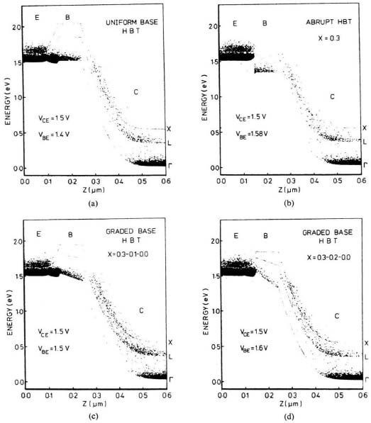
FIGURE 6.9 Electron energy distritutions for (a) a uniform doped base, (b) an abrupt injection barrier, (c) a grade mole fraction base, and (d) a graded base AlGaAs/GaAs HBTs (after Katoh etal., Ref. 11 © IEEE).
The collector depletion region has large electron fields in it resulting from the p-n junction, and at the base end it rises rapidly because of the heavy base doping. This results in rapid carrier heating in the depletion region in all the examples over a short distance, on the order of 500 Å. Carriers heat up in the valley, rapidly increasing in energy and velocity, and when they have sufficient energy they scatter into the X and L valleys, finally resulting in transport at the saturation velocity.
Electron drift velocity as a function of position for the structures of cases (a)–(d) is shown in Fig. 6.10. The velocity in the base varies from the drift-diffusion-like velocity of 2 to 4 × 106 cm/s in the uniformly doped base to higher velocities in the abrupt and graded base cases. The velocity in the collector rises very rapidly due to velocity overshoot and subsequently relaxes to approximately 107 cm/s saturation velocity of GaAs. The peak velocities are near the maximum group velocity.
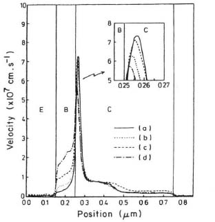
FIGURE 6.10 Electron drift velocity as a function of position (after Katoh et al., Ref. 11 © IEEE).
Electron energy as a function of position for a collector doping of 1 × 1017 cm−3 (a), 2 × 1017 cm−3 (b), a thickness collector of 5 × 1016 cm−3 with a p-extension of the base (c), and a 1 × 1017 cm−3 collector with a p-extensions of the base (d) is displayed in Fig. 6.11. For cases (a) and (b) in Fig. 6.11, the depletion region shrinks at the higher doping in the collector, with a corresponding increase in the electric field. This leads to a transfer of electrons to the L and X valleys occurring over a shorter distance. Cases (c) and (d) are of more interest because of the decrease in the electric field in the collector depletion region as well as the rapid change in the field by employing a p-type extension of the base region. The decrease in electric field, as a result, allows the carriers to overshoot over a longer distance because they do not pick up enough energy to transfer to the L and X valleys during the approximately 1000 Å of travel. In these structures, during the transit through the collector depletion region, the average velocity can be much larger, and the corresponding transit delay significantly shorter.

FIGURE 6.11 Electron energy versus position for various collector designs (after Katoh et al., Ref. 11 © IEEE).
Overshoot effects occur because the relaxation rate of momentum is larger than that of energy, and a major cause of these large rates is the large scattering rate resulting from the secondary valley transfer. Ga0.47In0.53 As, which has secondary valleys placed much higher than the primary valleys, may show stronger nonequilibrium effects than GaAs. The maximum possible velocities are related to this Γ–L separation and the effective mass of electrons. InP, which has a larger bandgap and hence a larger breakdown voltage. InAs is another contrasting choice because it has a very large secondary valley separation, an unusually low scattering rate and effective mass, but a small bandgap and hence a small breakdown voltage.
Consider the switching in heterojunction bipolar transistors. Figure 6.12 shows transient evolution of the potential (a), the kinetic energy (b), the carrier density (c), and the velocity (d) for a switching in VBE from 1.2 V to 1.4 V, with VBC maintained at 0 V of a GaAs HBT [12]. The collector doping is 1 × 1017 cm–3 with an expitaxial thickness of 0.175 μm, a compromise between excess storage delay due to the Kirk effect at the 1.4-V input bias and collector signal delay. Indeed, at the high input bias, evidence of the Kirk effect is observable in the conduction-band edge and electron density profiles of Fig. 6.12. The electron transit time, as a function of time, is observable in the collector space-charge region. However, the time taken for this transit (the collector transit time) is larger than the delay time of the collector current in the quasi-neutral collector (the collector signal delay), as explained in Section 4.2.6. Note that in Fig. 6.12 a broader velocity overshoot region develops, due to the presence of a larger electron density in the collector space charge at the higher bias. To generate this, consider the InP steady-state characteristics shown in Fig. 6.13. The peak velocity at the high bias is smaller than at the lower bias. This large bias case is actually quite similar to that of an extended lower doped base. With the switching to a higher bias at the base–emitter junction, the field in the base region decreases because of the higher electron density, and the high-field regions shift toward the collector–collector interface. The charge storage is larger. This occurs despite the collector transit time being smaller in this device. The collector signal delay is still larger. Therefore, both the analysis of the steady-state behavior alone and a strict emphasis on broadness of the overshoot can be deceiving. Similar comments also hold regarding small-signal behavior.
Steady-state behavior, however, does provide an adequate low-order description of the device behavior and is a good tool to compare the behavior of other materials and their behavior versus GaAs. Figure 6. 14 shows the steady-state behavior of the conduction-band edge energy, the kinetic energy, and the velocity in GaAs, InP, Ga0.47In0.53 As, and InAs under conditions of low Kirk effect. InP is of particular interest because of its larger secondary valley separation. This results in the broader but still peak overshoot behavior. Ga0.47In0.53 As HBTs have a secondary valley separation comparable to the bandgap, a smaller fraction of carrier transfer at this bias condition, and a broader overshoot. InAs is an extreme example in this comparison. It has a low scattering rate at low energies, a significantly larger secondary valley separation than the bandgap(> 1 eV separation compared to ≈ 0.4 eV bandgap), and hence only a few carriers transfer to the secondary valleys. Consequently, InAs bipolar transistors show the broadest and highest overshoot features of all these devices.

FIGURE 6.12 (a) Conduction-band energy, (b) kinetic energy, (c) electron density, and (d) velocity versus position as a function of time (after Tiwari et al., Ref. 12 © IEEE).
6.3 DRIFT AND DIFFUSION EQUATIONS
Standard drift and diffusion simulation is useful for semiconductor device analysis because of its computation efficiency. The drift–diffusion model assumes isothermal (or constant lattice temperature) and solves the five basic semiconductor equations: namely, Poisson’s equation,
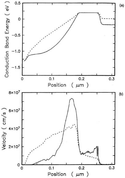
FIGURE 6.13 (a) Conduction-band energy and (b) velocity versus position for an InP HBT in low and high injection levels (after Tiwari et al., Ref. 12 © IEEE).
the continuity equations for electrons and holes,
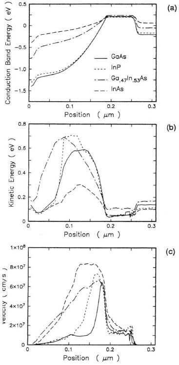
FIGURE 6.14 (a) Conduction-band energy, (b) kinetic energy, and (c) velocity of GaAs, Ga0.47In0.53 As, and InAs.
and the electron and hole current density equations,
In (6.19)–(6.23) ε is the permittivity, ψ the electrostatic potential, ![]() the ionized donor concentration,
the ionized donor concentration, ![]() the ionized acceptor concentration, ρF the fixed charge density that may be present due to fixed charge in insulating materials or charged interface states, t the time, Jn the electron current density, Jp the hole current density, Un the electron recombination rate, and Up the hole recombination rate.
the ionized acceptor concentration, ρF the fixed charge density that may be present due to fixed charge in insulating materials or charged interface states, t the time, Jn the electron current density, Jp the hole current density, Un the electron recombination rate, and Up the hole recombination rate.
When the semiconductor is lightly doped, the use of Boltzmann statistics is adequate in determining the Fermi level and carrier concentration:
where NC and NV are the density of states for conduction-band and valence band, EC and EV are the energy levels at the bottom of the conduction-band and at the top of the valence band, respectively, and EF is the Fermi level.
It is, however, necessary to use Fermi–Dirac statistics to calculate the Fermi level when the semiconductor is heavily doped (> 1018 cm−3):
where F1/2 is the Fermi–Dirac integral of order ![]() .
.
![]()
and ηn = (EFn – EC)/kT and ηρ = (EV – EFp)/kT. Although for most practical cases, full impurity ionization is assumed (i.e., ![]() and
and ![]() ), the device simulators are able to model the incomplete ionization due to carrier freeze-out effect
), the device simulators are able to model the incomplete ionization due to carrier freeze-out effect
where gc is the degeneracy factor for electrons, gd the degeneracy factor for holes, EFn the electron quasi-Fermi level, EFp the hole quasi-Fermi level, ED the donor energy level, and EA the acceptor energy level.
In the continuity equations for electrons and holes, Shockley–Read–Hall and Auger recombination models are used:

where Ei is the intrinsic energy level, ET the trap density energy level, τn, the electron lifetime, and τp the hole lifetime.
The intrinsic concentration, energy bandgap, effective density of states for the conduction-band, and density of states for the valence band are temperature dependent
where α = 4.73 × 10⁻⁴ for Si and 5.405 × 10⁻⁴ for GaAs and β = 636 for Si and 204 for GaAs [13]. A list of α and β for various compound semiconductors is given in Table 6.1.
TABLE 6.1 Values of α and β in (6.35) for Various III/V Compound Semiconductors

The electron and hole mobilities as a function of concentration and temperature are expressed as [2]
for Si and
for GaAs.
The diffusion coefficients are related by the Einstein relation
for nondegenerate semiconductors and
for degenerate semiconductors.
When solving for structures that contain heterojunctions, the intrinsic Fermi potential is in general not a solution to Poisson’s equation. The vacuum level, however, is a solution to Poisson’s equation. The intrinsic Fermi potential and vacuum level are related by
where ψ is the intrinsic Fermi potential and θ is the band structure parameters given by
Note that if the band structure parameter is spatially constant, ψ will be a solution to Poisson’s equation. However, this is seldom the case in structures containing heterojunctions due to differences in bandgap, electron affinity, and densities of states in adjacent materials. Thus Poisson’s equation must be written in the form
The form of the continuity equations remains unchanged for the heterojunction except that the electric field terms En and Ep in the transport equations must account for gradients in conduction- and valence-band edges:
The material parameters available for describing the properties of the heterojunction are just the usual parameters available for describing the properties of the materials that meet at the heterojunction. Some of these include the energy bandgap parameters, electron affinity, and densities of states, as well as the various parameters for describing recombination, mobility, and so on.
6.4 HYDRODYNAMIC EQUATIONS
The drift–diffusion approximation can lead to unacceptable inaccuracies in the predicted electrical characteristics of modern devices. For example, when the base thickness of the heterojunction bipolar transistor is made very thin, electrons injected into the base encounter only a few collisions before reaching the collector. High-energy electrons transverse across the thin base ballistically. Conventional drift and diffusion mechanisms used to describe carrier transport become invalid. To describe the movement of electrons accurately in the thin-base bipolar transistor, the use of Monte Carlo simulation is essential. Monte Carlo simulations, however, are extremely time consuming and not useful for studying device terminal currents. Hydrodynamic or energy balance model s have become popular as a way of accounting for nonlocal transport effects to emulate the Monte Carlo simulation behavior. The solutions of the standard hydrodynamic equation are approximations to the lowest three moments of the Boltzmann transport equations.
Furthermore, in device simulation it is typically assumed that the carrier transport is always isothermal, and the carriers are always in a quasi-static state such that a direct relation between the carrier energy and the local electrical field exists. The first assumption eliminates the carrier flux component driven by the temperature gradient, while the second allows the use of local field-dependent relationships for carrier transport parameters such as the carrier mobility. Since only potential and carrier concentrations are included in the solutions, it is assumed implicitily that dissipated power density inside devices is so low that no significant lattice temperature increase occurs. These assumptions, however, begin to fail for heterojunction semiconductor devices on the GaAs semi-insulating substrate, where self-heating is significant. Moreover, hot carrier nonlocal transport such as velocity overshoot begins to emerge due to the large field gradient and the finite-energy relaxation rate. Consequently, a full thermodynamic (nonisothermal) solution is needed to account for nonuniform lattice temperature for more accurate device performance prediction.
The complete thermodynamic system consists of a set of additional partial differential equations in conjunction with standard drift and diffusion equations. These additional equations are the particle energy balance equations for electrons and holes:
and the lattice energy-balance equation
where Sn and Sp are the energy flux densities associated with electrons and holes, Wn and Wp are the energy density loss rates for electrons and holes, and H is the heat source for the lattice.
The hydrodynamic set of equations uses generalized expressions for the electron and hole current densities [2]:

Figure 6.15 shows the Gum mel plot of the heterojunction simulation using MEDICI. It is obvious from Fig. 6.15 that self-heating increases the collector and base currents at high base–emitter biases. The nonuniform temperature distribution of the HBT biased at VBE = 1.5 V is shown in Fig. 6.16. The effect of self-heating affects the Early voltage of the bipolar transistor significantly. Figure 6.17 shows the simulated Early voltage of a bipolar device using drift diffusion and the energy balance equation versus the collector current. The standard drift-diffusion simulation predicts an increase of the Early voltage at high collector currents. The energy balance simulation, however, gives a decrease of the Early voltage at high collector currents. The latter simulation accounts for device self-heating, which reduces the Early voltage of the bipolar device.

FIGURE 6.15 Simulated collector and base currents versus base–emitter bias.
The coupling effect of the AlGaAs/GaAs HBT between nonlocal charge transport and nonisothermal behavior was investigated [16]. The Al0.3Ga0.7 As emitter has a width of 0.15 μm, with the last 30 nm graded. The GaAs base, n− collector, and n+ collector widths are 0.1, 0.5, and 0.15 μm, respectively. The doping concentrations in the emitter, base n− collector, and n+ collector are 5 × 10¹⁷, 1019, and 1017m and 1018 cm−3, respectively. The lengths of the emitter and collector are 1 and 4 μm. A thermal resistor with a value of Rth = 6.7 × 10⁻⁴ K·cm/W connects the bottom of the device to a heat sink held at 300 K. Figure 6.18 shows the cutoff frequency of the HBT simulated by drift–diffusion (DD), nonisothermal drift–diffusion (NDD), energy balance (EB), and nonisothermal energy balance (NEB). Significant differences between the results calculated using the DD and EB models were observed. This is because the EB model accounts for velocity overshoot, which reduces the base–collector transit time, thereby increasing the cutoff frequency. Inclusion of the nonisothermal model reduces the cutoff frequency at high collector current compared to that of the EB model. The nonisothermal energy-balance model predicts significant negative differential resistance (NDR) as shown in Fig. 6.19. The drift–diffusion model predicts no NDR. The nonisothermal drift–diffusion model predicts much less pronounced NDR. The energy-balance model predicts NDR over only a limiting range of bias voltage.

FIGURE 6.16 Temperature distribution of an HBT in MEDICI simulation.
The Monte Carlo, energy balance, and drift–diffusion simulations for a SiGe HBT were compared [17]. Figure 6.20 shows the electric field, energy, velocity, and electron concentration versus position of the SiGe HBT. The electric field is virtually the same as that predicted by these three simulations. However, the energy distribution predicted by the energy balance simulation is closer to the Monte Carlo simulation, while the drift–diffusion simulation predicts a uniform energy distribution, as shown in Fig. 6.20b. The velocity overshoot profiles between the MC and EB simulations are pretty much the same, while the drift–diffusion simulation projects a uniform saturation velocity. In Fig. 6.20c the electron velocity for 150 nm < x < 300 nm predicted by the MC and EB simulations is lower that of the drift–diffusion result. This is due to an enhancement of electron concentration in that region, as shown in Fig. 6.20d. For a given set of boundary conditions (VBE = 0.7 V and VCE = 1.0 V), the electron velocity is reduced when the electron concentration is increased to maintain a constant collector current density.

FIGURE 6.17 Early voltage versus collector current (after Liang and Law, Ref. 15 © IEEE).
6.5 TRANSISTOR DESIGN USING HETEROJUNCTION DEVICE SIMULATION
Device simulators are powerful tools that model the two- or three-dimensional distributions of potential and carrier concentrations as well as current vectors in a device and predict the device electrical characteristics for any bias condition. Simulators are useful not only for majority-carrier devices, which involve a single carrier type such as the MESFET and MODFET, but also for minority-carrier devices, which involve both carriers (electrons and holes) such as HBTs. The device can be simulated under steady-state, small-signal, and transient operating conditions.
In general, device simulation provides the ability to perform computer simulation experiments without using semiconductor wafers. The simulation is transparent to semiconductor technologies and independent of expensive fabrication equipment. In addition, the turnaround design time of advanced or prototype devices is reduced. Efficient use of device simulators, however, requires knowledge of semiconductor device physics for the insightful interpretation of device simulation results. The accuracy of device simulation relies heavily on the physical parameters used in the simulator. The simulation results are sensitive to the design of mesh points, especially for non-planar device structures. In addition, the accuracy of the doping profile is important, especially for small-geometry devices. Nevertheless, device simulation provides a relatively accurate model of device response with respect to boundary conditions. It also provides insight into device operation and doping profile optimization.

FIGURE 6.18 Cutoff frequency versus collector current (after Apanovich et al., Ref. 16 © IEEE).
There are many device simulators available, such as SEDAN [18], PISCES [19], BIPOLE [20], BAMBI [21], MINIMOS [22], MEDICI [2], DAVINCI [23], and ATLAS [24]. Here we use the device simulator MEDICI for illustration purposes. MEDICI accurately describes the behavior of deep submicron devices by providing the ability to solve the electron and hole energy balance equations consistently with the other device equations. Effects such as carrier heating and velocity overshoot are accounted for. Many physical models are incorporated into the program. Among these are models for recombination, mobility, and lifetime. Both Boltzmann and Fermi-Dirac statistics, including the incomplete ionization of impurities and effect of carrier freeze-out, are included. The simulator is able to attach lumped resistors, capacitors, and inductors to contacts as well as distributed contact resistances. Both voltage and current boundary conditions during a simulation can be specified. In addition, a light source can be specified for examining the photoelectrical response of photodiodes and phototransistors. Advanced application modules (AAMs) are available. The lattice temperature AAM is able to solve the lattice heating equation self-consistently with the other device equations. The heterojunction device AAM simulates the heterojunction device behavior.
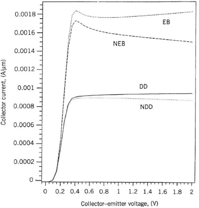
FIGURE 6.19 Collector current versus collector-emitter voltage (after Apanovich et al., Ref. 16 © IEEE).
With its nonuniform triangular simulation grid, MEDICI can model arbitrary device geometries with both planar and nonplanar surface topologies. From the grid structure of the device and impurity doping profile, MEDICI used the finite element method for solving the five basic semiconductor equations. The finite element method lends itself to structures that are far from rectangular. Since they employ elements that can be quite different in size for different regions, the method is also ideal for having small elements in the vicinity of junctions, where the potential is rapidly changing. The boundary conditions are incorporated as integrals in a function that is minimized, and the scheme is independent of the specific boundary conditions; this provides a good degree of flexibility, particularly since elements of different sizes may be added without increasing the complexity.

FIGURE 6.20 (a) Electric field, (b) electron energy, (c) velocity, and (d) electron concentration versus position for a SiGe HBT (after Nuembergk et al., Ref. 17 © IEE).
MEDICI uses the box method to discretize the differential operators on a general triangular grid. Each equation is integrated over a small polygon enclosing each node. The integration equates the flux into the polygon with the sources and sinks inside it so that conservation current and electric flux are built into the solution. The integral involved is performed on a triangle-by-triangle basis, which leads to a simple and elegant way of handling general surface and boundary conditions.
The discretization of the semiconductor device equations gives rise to a set of coupled nonlinear algebraic equations which must be solved by a nonlinear iteration method starting from an initial guess. Two approaches are widely used: Gummel’s method and Newton’s method. In Gummel’s method, the equations are solved sequentially. Poisson’s equation is solved assuming fixed quasi-Fermi potentials; since Poisson’s equation is nonlinear, it is solved by an inner Newton loop. Then the new potential is substituted into the continuity equations, which are linear and can be solved directly. The new carrier concentrations are substituted back into the charge term of Poisson’s equation and another cycle begins. At each state only one equation is being solved, so the matrix has N rows and N columns, regardless of the number of carriers being solved. This is a decoupled method; one set of variables is held fixed while another set is solved. The success of the method therefore depends on the degree of coupling between the equations. In Newton’s method, all of the variables in the problem are allowed to change during each iteration, and all of the coupling between variables is taken into account. Due to this, the Newton method is very stable and the solution time is nearly independent of bias condition even at high levels of injection. Each approach involves solving several large linear systems of equations. The number of equations in each system is on the order of one to three times the number of grid points, depending on the number of carriers being solved for. The nonlinear iteration usually converges either at a linear rate or at a quadratic rate. In the former, the error decreases by about the same factor at each iteration. In a quadratic method, the error should go down at each iteration, giving rise to rapid convergence. For accurate solutions, it is advantageous to use a quadratic method. Newton’s method is quadratic, whereas Gummel’s method is linear in most cases.
A solution is considered converged, and iterations will terminate, when either the X norm falls below a certain tolerance or the right-hand-side (RHS) norm falls below a certain tolerance. The X norm measures the error as the size of the updates to the device variables at each iteration. For the X norm, the default tolerance is 10−5 kT/q for the potentials and 10−5 relative change in the concentrations. The RHS norm measures the error as a function of the difference between the left- and right-hand sides of the equations. For the RHS norm, the tolerance is 10−26 C/μm for the continuity equations. By default, MEDICI uses a combination of the X norm and RHS norm to determine convergence, and therefore alleviates the difficulty of choosing one method or the other. Basically, the program assumes that a solution is converged when either the X norm or RHS norm tolerances are satisfied at every node in the device. This often greatly reduces the number of iterations required to obtain a solution, compared to when either the X norm or RHS norm is used alone, without sacrificing the accuracy of the solution.
The correct allocation of the grid is a crucial issue in device simulation. The number of nodes in the grid has a direct influence on the simulation time. Because the different parts of a device have very different electrical behavior, it is usually necessary to allocate a fine grid in some regions and a coarse grid in others to maintain reasonable simulation time. Another aspect of grid allocation is the accurate representation of small-device geometries. To model the carrier flow correctly, the grid must be a reasonable fit to the device shape. This consideration becomes more and more important as smaller, more non planar devices are simulated. MEDICI supports a general irregular grid structure. This permits the analysis of arbitrarily shaped devices and allows the refinement of particular regions with minimum impact to others.
Because of the extremely rigid mathematical nature of Poisson’s equation and the electron and hole current continuity equations, strong stability requirements are placed on any proposed transient integration scheme. Additionally, it is most convenient to use one-step integration methods so that only the solution at the most recent time step is required. MEDICI has made use of the first-order (implicit) backward difference in time formula; that is, electron and hole concentrations are discretized as
where Δtj = tj − tj − 1 and ψj, nj, and pj denotes the potential, electron concentration, and hole concentration at time tj, respectively. The backward Euler method is known to be both A- and L-stable, but suffers from a large local truncation error (LTE), which is proportional to the size of the time steps taken.
The backward Euler method is a one-step method. An alternative to the backward Euler method is the second-order backward difference formula
where γ = (tj − 1 − tj − 2)/(tj − tj − 2). At a given point of time, MEDICI checks the local truncation error for both the first- and second-order backward difference methods and selects the method that yields the largest time step. By default MEDICI will select time steps so that the local truncation error matches the user-specified criteria. Specifying a larger tolerance will result in a quicker but less accurate simulation. MEDICI also places additional restrictions on the time steps:
(1) The time step size is allowed to increase at most by a factor of 2.
(2) If the new time step is less than half of the preceding step, the preceding time step is recalculated.
(3) If a time point fails to converge, the time step is reduced by a factor of 2 and the point is recalculated.
In addition to steady-state and transient simulation, MEDICI also allows small-signal analysis to be performed. An input of given amplitude and frequency can be applied to a device structure from which sinusoidal tern1inal currents and voltages are calculated. In MEDICI, the use of small-signal device analysis published by Laux [25] is adopted. An ac sinusoidal voltage bias is applied to an electrode i such that
where Vi0 is the dc bias, ![]() the small-signal amplitude, ω the angular frequency, and Vi the actual bias (sum) to be simulated. Rearranging the basic partial differential equations in (6.19)–(6.21), we obtain
the small-signal amplitude, ω the angular frequency, and Vi the actual bias (sum) to be simulated. Rearranging the basic partial differential equations in (6.19)–(6.21), we obtain
The ac solution to the equations above can be written as
where ψi0, ni0, and pi0 are the dc potential and carrier concentrations at node i, while ![]() ,
, ![]() , and
, and ![]() are the respective ac values. By substituting (6.62)−(6.64) into (6.59)−(6.61) and expanding as a Taylor series of first order only, one obtains nonlinear equations of the form for each of the three partial differential equations
are the respective ac values. By substituting (6.62)−(6.64) into (6.59)−(6.61) and expanding as a Taylor series of first order only, one obtains nonlinear equations of the form for each of the three partial differential equations
The heterojunction device simulation can be used to investigate different device design [26−28]. Liou [28] used the MEDICI simulation to study three different HBTs: the emitter island (E-island), emitter-base island (E/B-island), and emitter-base/collector (E/B/C-island) structure as shown in Fig. 6.21a–c, respectively. Device dc and RF characteristics were examined. Through the analysis, all three HBT structures have N-p+-n Al0.3Ga0.7As/GaAs three-finger HBTs with the following practical makeup: a 5 × 1018 cm−3 and 1000-Å emitter, 300-Å graded layer, 1019 cm−3 and 1000-Å base, 5 × 1016 cm−3 and 7000-Å collector, 4 × 10 μm2 emitter finger area, and 10-μm finger spacing.
Figure 6.22 shows the current gain versus the collector current of the three HBTs simulated at VCE = 2 and 5 V, respectively. It is clear that the E-island HBT has the highest current gain for a wide range of collector currents. This is due to the fact that the lattice temperature in such a device is the lowest among the three HBTs, as evidenced by the lattice temperature contours in Fig. 6.23. The current gain at high collector current(> 10−4A/μm) decreases with increasing IC and VCE due to self-heating. Note that the intrinsic HBT is located at 0 < y < 0.93 μm and 234 μm < x < 266 μm, and the lattice temperature decreases rapidly toward the sidewalls and semi-insulating substrate. Also, the middle finger is hotter than the outer fingers, due to the thermal coupling among the fingers. At low collector current (< 10−6 A/μm) the largest current gain in the E-island HBT results from the continuous base structure, which makes the electron-hole recombination in the base less prominent and hence reduces the base current. Intuitively, one expects that the E/B-island HBT has a lower lattice temperature than the E/B/C-island HBT, due to a more uniform collector formation. This is not the case, however, because the contiguous collector in the E/B-island HBT results in a more uniform current contour in the collector and thus a higher collector current. The higher collector current consequently gives rise to a more significant thermal effect and a higher lattice temperature in the E/B-island HBT than in its E/B/C-island counterpart.

FIGURE 6.21 (a) Emitter-island, (b) emitter/base-island, and (c) emitter/base/collector-island HBTs (after Liou, Ref. 28 © Artech House).

FIGURE 6.22 (a) Current gain versus collector current at VCE = 2 V (after Liou, Ref. 28 © Artech House).
Figure 6.24 shows the cutoff frequency of the three HBTs simulated at VCE = 2 and 5 V, respectively. Like the current gain, the high-current fT degradation at larger VCE is due to thermal effect. At low collector current, however, fT is slightly higher at larger VCE, due to a larger electric field in the base–collector junction and a smaller quasi-neutral base thickness as VCE increased. Furthermore, the simulation results show that the E/B/C-island HBT has the lowest peak fT, attributed to the fact that the E/B/C-island HBT has the least uniform electric field in the base–collector junction among the three devices. It has been shown that the free-carrier transit time across the base–collector space-charge region is often the limiting factor for the HBT cutoff frequency. Thus the lower field in the regions between fingers found in the E/B-and E/B/C-island HBTs increases the overall transit time and decreases the cutoff frequency of the HBTs.

FIGURE 6.22 (b) Current gain versus collector current at VCE = 5 V (after Liou, Ref. 28 © Artech House).
Advanced epitaxial growth of strained SiGe into a Si substrate enhances the free form for designing high-speed bipolar transistors. The use of device simulation helps the design of an optimized Ge profile in the base to achieve the best electrical characteristics, such as current gain and cutoff frequency. Hueting et al. [29] used the one-dimensional device simulator HeTRAP to study the optimization of SiGe-base bipolar transistors. The effect of the position of the leading edge of the Ge profile relative to the emitter–base metallurgical junction (distance d) on the HBT electrical performance was investigated. The maximum cutoff frequency and the current gain as a function of the distance d is shown in Fig. 6.25. Three regions of d are defined in Fig. 6.25. In region 1 the Ge edge is in the emitter–base space-charge region. Here the Ge causes extra bandgap narrowing and increased storage time, which reduces fT,max. Shifting the profile edge to region 2 increases fT,max but decreases the current gain. In this region the base Gummel number is very sensitive to VBE. Increasing the distance d causes an enhancement of the base Gummel number. This reduces the collector current density. Consequently, the current gain is reduced. In region 3 the profile edge enters deeper into the neutral base region, causing a considerable reduction in the collector current density and current gain. The peak cutoff frequency fT,max, however, decreases only slightly with increasing distance.
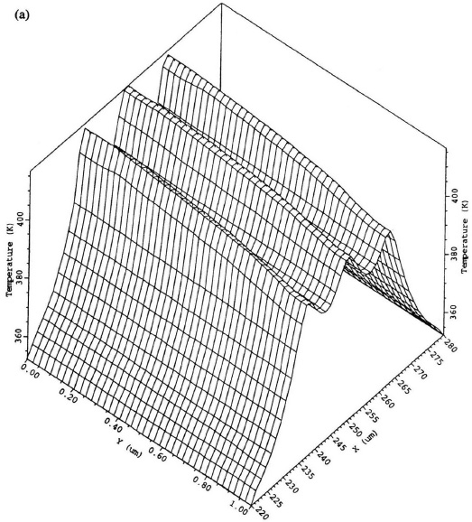
FIGURE 6.23 (a) Lattice temperature contours in the E-island HBTs at VBE = 1.5 V and VCE = 2.0 V (after Liou, Ref. 28 © Artech House).
Note that the slopes of both curves in Fig. 6.25 depend on the device structure, temperature, collector–base voltage, and Ge percentage. Only regions 1 and 3 have ideal Gummel plots. In region 2 the Ge profile is rather close to the emitter–base space charge, and this causes a parasitic energy barrier that strongly varies with the emitter–base bias. This modulates the base Gummel number and introduces strong nonideal IC−VBE characteristics. If the Ge profile reaches beyond region 3, a much larger SiGe layer thickness would be needed. This increases the risk of misfit dislocations in the material. Therefore, the optimal position of the Ge profile is in region 3.

FIGURE 6.23 (b) Lattice temperature contours in the E/B-island HBTs at VBE = 1.5 V and VCE = 2.0 V (after Liou, Ref. 28 © Artech House).
The various transit times between the Si BJT and SiGe HBT are compared [30]. The comparison is based on the charge partitioning method (quasistatic approximation) presented by van den Biesen [31]. From the integration of charge of two very similar operating points, one gets the emitter-to-collector transit time

FIGURE 6.23 (c) Lattice temperature contours in the E/B/C-island HBTs at VBE = 1.5 V and VCE = 2.0 V (after Liou, Ref. 28 © Artech House).


FIGURE 6.24 (a) Cutoff frequency versus collector current at VCE = 2 V (after Liou, Ref. 28 © Artech House).
while the transit time within the different regions of a device is given by
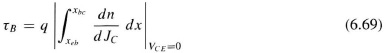

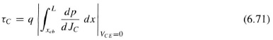

FIGURE 6.24 (b) Cutoff frequency versus collector current at VCE = 5 V (after Liou, Ref. 28 © Artech House).
Note that τE, τB, and τC are influenced by the neutral, mobile charge stored in the emitter, base, and collector. τEB and τBC are the charging times for the space-charge regions. The boundary conditions Xbe and Xbc are determined from the intersection of the curves |dn/dJC|VCE=0 and |dp/dJC|VCE=0. Therefore, xbe and xbc are not the usual boundaries for the space-charge regions.
Figure 6.26 shows a comparison of various transit times for a Si BJT and a SiGe HBT. As shown in Fig. 6.26, the collector–emitter transit time has been reduced significantly for the SiGe HBT, due to reduction of base transit time and emitter transit time resulting from the introduction of Ge in the base.
6.6 MULTlEMITTER SIMULATION
The heterojunction bipolar transistors use multiemitter fingers to achieve excellent RF performance while maintaining dc current driving capability. The emitter finger width and spacing effects could only be studied by using three-dimensional analysis. Figure 6.27 shows the schematic diagram of conventional HBT chip with multiemitter fingers fabricated on the top surface of a GaAs substrate. Each emitter finger is further divided into a number of unit areas. Each unit area is assumed to be a heat source with constant temperature, with the exception of the substrate bottom surface, where the temperature is kept at heat sink temperature T0 and the heat sources on the top.

FIGURE 6.25 Peak cutoff frequency and current gain versus distance (after Hueting et al., Ref. 29 © IEEE).

FIGURE 6.26 Comparison of transit times of a BJT and a SiGe HBT.
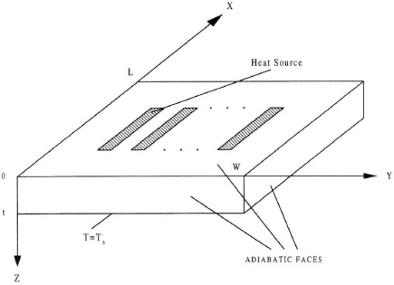
FIGURE 6.27 Multiemitter fingers on the top surface of a GaAs substrate.
The remaining surfaces are assumed adiabatic. Using these boundary conditions

the temperature distribution at the top surface (i.e., z = 0) can be obtained by solving the heat transfer equation
If thermal conductivity is temperature independent [κ(T) = κ0], the solution is given by [32,33]

qi Δx Δy is the heat generated at ith unit area with the center located at (xi, yi), Δx Δy the unit area, N the number of the unit area on the surface, κ0 the thermal conductivity at the heat sink temperature, and Lx, Ly, and d are the x, y, and z-dimensions, respectively. Kirchhoff’s transformation can be used to account for the temperature-dependent thermal conductivity. Assuming that the thermal conductivity is proportional to (T/T0)−1.22, the corrected temperature is
where θ is as given in (6.73).
The effect of chip thickness on HBT thermal behavior is shown in Fig. 6.28. Both the active region and substrate are assumed to have a square shape. La/ Lc is the ratio of side lengths between the active region and the substrate. If this ratio is equal to 0.8, which is typical of conventional Si power transistors, the peak junction temperature decreases almost linearly with the decrease in chip thickness. However, if the ratio is less than 0.5, thinning of the substrate has little impact on peak junction temperature based on the result of the three-dimensional thermal analysis. Where the dimension of the active region is much less than the chip size, the heat flow is distributed in a cone shape, and the junction temperature is determined primarily by the lateral size of the device rather than the chip thickness.
Analytical and experimental results used to investigate thermal behavior depending on the emitter-finger area and substrate thickness in multifinger HBTs were also published [34]. As the substrate thickness decreases from 100 μm to 30 μm under the fixed power dissipation condition, the peak temperature of the large-emitter-area HBT (Fig. 6.29) decreases from 373 K to 346 K, while that of the small-emitter-area HBT (Fig. 6.30) decreases to 367 K. Thermal resistance Rth (= Tj − T0/dissipate power) of the large-emitter-area HBT decreases from 40°C/W to 25°C/W, while the Rth values of the small-emitter-area HBT decreases from 200°C/W to l86°C/W. A reduction in Rth is obtained in the large-emitter-area HBT, while only a small reduction of 7% is obtained in the small-emitter-area HBT.
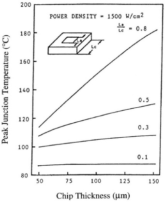
FIGURE 6.28 Effect of chip thickness (after Gao et al., Ref. 32 © IEEE).
Clearly, the junction temperature in the larger-emitter-area HBT decreases significantly when the substrate is thinned. This can be explained in term of the three-dimensional effect of the heat flow. As the emitter-finger area becomes smaller, the three-dimensional effect becomes dominant, and the heat concentrates in the vicinity of the emitter fingers. In this case, the junction temperature decreases very gradually with the thinning of the substrate. On the other hand, as the emitter-finger area becomes larger, the three-dimensional effect weakens, and the heat spreads over the entire chip. In this case the junction temperature decreases significantly with thinning of the substrate.
Three-dimensional transmission-line matrix simulation was used to evaluate the thermal behavior of power HBTs with multiple-emitter fingers [35]. The power device consists of five cells. Each cell has two emitter fingers grouped closely together by the emitter–base self-alignment process. The temperature distribution is simulated at a dissipated power density of 2 mW/μm2 under steady state. Figure 6.31 shows the isometric view of temperature distribution of five emitter fingers, and Fig. 6.32 is the contour plot with interval of l5°C. The isometric projection and the corresponding temperature contours clearly display that two peak values of junction temperature occur at the centers of the two central emitter fingers. The junction temperature drops sharply around the central cell, with an average temperature gradient as high as 9°C/μm in these areas. From a device-reliability point of view, the peak junction temperature is the most important parameter for the device thermal design and should be used to characterize the device thermal behavior.

FIGURE 6.29 Three-dimensional temperature distribution of a 40 × 4 μm2 HBTat a substrate thickness of (a) 100 μm and (b) 30 μm; the dissipated power is fixed at 1.7 W (after Kim et al., Ref. 34 © IEEE).
The nonuniform junction temperature distribution of HBTs for various substrate materials is depicted in Fig. 6.33. The peak junction temperatures are 180, 140, and 101°C for the HBTs on GaAs, lnP, and Si substrates, respectively. The HBT on a Si substrate obviously operates better than others for the same power dissipation.
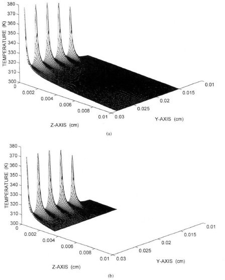
FIGURE 6.30 Three-dimensional temperature distribution of a 2.7 × 4 μm2 HBT at a substrate thickness of (a) 100 μm and (b) 30 μm; the dissipated power is fixed at 0.34 W (after Kim et al., Ref. 34 © IEEE).
In the design of power heterojunction bipolar transistors, the emitter-finger length is determined primarily by the emitter metallization resistance and the junction temperature nonuniformity along the emitter length. In general, the length and the length/width ratio of an emitter finger should not exceed 30 μm and have a 20:1 ratio in order to minimize the junction temperature and the voltage drop along the length of the finger. From thermal considerations, a power HBT with a longer emitter length results in a higher junction temperature and in turn causes a reduction in the output power density.

FIGURE 6.31 Isometric view of temperature distribution of five emitter fingers (after Gui et al., Ref. 35 © IEEE).
The total emitter area is determined by the desired output power or the maximum peak collector current. For silicon bipolar transistors, the peak current is strongly dependent on the emitter periphery, due to current crowding at high currents. For HBTs with high base doping concentration, the emitter crowding effect is reduced significantly. The calculated emitter utilization factor as a function of operating frequency and emitter size is depicted in Fig. 6.34. Clearly, an emitter width of 2 μm is sufficient for an operating frequency of 10 GHz. In this case, the emitter utilization factor should be greater than 95%. This allows the current capability and the output power for HBTs to be dependent on the emitter area rather than the emitter periphery.

FIGURE 6.32 Contour plot of temperature distribution (after Gui et al., Ref. 35 © IEEE).

FIGURE 6.33 Junction temperature distribution for different substrate materials (after Gao et al., Ref. 36 © IEEE).

FIGURE 6.34 Emitter utilization factor as a function of frequency (after Gao et al., Ref. 36 © IEEE).

FIGURE 6.35 Peak junction temperature versus emitter spacing (after Gao et al., Ref. 36 © IEEE).
Another very important parameter for multiple-emitter-finger HBT design is the emitter spacing, which is defined as the center distance between two adjacent emitter fingers. A larger spacing results in a higher base resistance and capacitance, both of which degrade the fmax or the power gain. On the other hand, a larger spacing reduces the peak value of junction temperature at a given power dissipation, as seen in Fig. 6.35. When the spacing increases from 4.4 μm to 6, 10, and 14 μm, the peak value of junction temperature is reduced by 17.5, 35.0, and 42.5%, respectively, for a power density of 2 m W/μm2.
REFERENCES
1. SUPREM IV: Two-Dimensional Semiconductor Process Simulation, Technology Modeling Associates, Inc., Palo Alto, CA (1993).
2. MEDICI : Two-Dimensional Semiconductor Device Simulation, User’s Manual, Technology Modeling Associates, Inc., Palo Alto, CA (1993).
3. L. W. Nagel, SPICE2: A Computer Program to Simulate Semiconductor Circuits, Electronics Research Laboratory Report ERL-M520, University of California, Berkeley, CA (1975).
4. M. V. Fischett and S. E. Laux, “Monte Carlo analysis of electron transport in small semiconductor devices including band structures and space charge effects,” Phys. Rev. B, 38, 9721 (1988).
5. D. T. Hughes, R. A. Abram, and R. W. Kelsall, “An investigation of graded and uniform base GexSi1−x HBTs using a Monte Carlo simulation,” IEEE Trans. Electron Devices, ED-42, 201 (1995).
6. B. K. Ridley, Quantum Processes in Semiconductors, University Press, Oxford, Oxford (1993).
7. R. Katoh and M. Kurata, “A model-based comparison of AlInAs/GaInAs and InP/GaInAs HBTs: a Monte Carlo study,” IEEE Trans. Electron Devices, ED-37, 1245 (1990).
8. S. Adachi, “Material parameters of In1−x Gax Asy, P1−y and related binaries,” J. Appl. Phys., 53, 846 (1989).
9. S. Adachi, “GaAs, AlAs, and AlxGa1−x As: material parameters for use in research and device applications,” J. Appl. Phys., 58, R1 (1985).
10. K. Brennan and K. Hess, “High field transport in GaAs, InP, and InAs,” Solid-State Electron., 27, 237 (1984).
11. R. Katoh, M. Kurata, and J. Yoshida, “Self-consistent particle simulation for (Al,Ga)-As/GaAs HBTs with improved base–collector structures,” IEEE Trans. Electron Devices, ED-36, 846 (1989).
12. S. Tiwari, M. Fischetti, and S. E. Laux, “Transient and steady-state overshoot in GaAs, InP, Ga0.47 In0.53 As, and InAs bipolar transistors,” IEDM Tech. Dig., 435 (1990).
13. S. Sze, Physics of Semiconductor Devices, 2nd ed., Wiley, New York (1981).
14. H. C. Casey, Jr., and M. B. Panish, Heterostructure Lasers: Part B. Materials and Operating Characteristics, Academic Press, San Diego, CA (1978).
15. M. Liang and M. E. Law, “Influence of lattice self-heating and hot-carrier transport on device performance,” IEEE Trans. Electron Devices, ED-41, 2391 (1994).
16. Y. Apanovich, P. Blakey, R. Cottle, E. Lyumkis, B. Polsky, A. Shur, and A. Tchemiaev, “Numerical simulation of submicrometer devices including coupled nonlocal transport and non isothermal effects,” IEEE Trans. Electron Devices, ED-42, 890 (1995).
17. D. M. Nuernbergk, H. Forster, F. Schwierz, J. S. Yuan, and G. Paasch, “Comparison of Monte Carlo, energy transport, and drift−diffusion simulations for a Si/SiGe/Si HBT,” High Peiformance Electron Devices for Microwave and Optoelectronics Applications, London, Nov. 24−25 (1997).
18. TMA SEDAN-2: One-Dimensional Device Analysis Program, User ’s Manual, Technology Modeling Associates, Inc., Palo Alto, CA (1984).
19. PISCES: Two-Dimensional Device Analysis Program, User’s Manual, Technology Modeling Associates, Inc., Palo Alto, CA (1989).
20. BIPOLE3: Bipolar Semiconductor Device Simulation, User’s Manual, Technology Modeling Associates in conjunction with Electrical and Computer Engineering Department, University of Waterloo (1993).
21. A. F. Franz, G. A. Franz, W. Kausel, G. Nanx, P. Dickinger, and C. Fischer, BAMBI 2.1 User’s Guide, Institute for Microelectronics, Technical University, Vienna (1989).
22. C. Fischer, P. Habas, O. Heinreichsberger, H. Kosina, Ph. Lindorfer, P. Pichler, H. Potzl, C. Sala, A. Schutz, S. Selberherr, M. Stiftinger, and M. Thurner, MINJMOS 6.0, User ’s Guide, Institute for Microelectronics, Technical University, Vienna (1994).
23. DAVINCI, Three-Dimensional Semiconductor Device Simulation, Technology Modeling Associates, Inc., Palo Alto, CA (1993).
24. ATLAS User Manual, Device Simulation Software, Silvaco International, Inc., Santa Clara (1996).
25. S. E. Laux, ’Techniques for small-signal analysis of semiconductor devices,” IEEE Trans. Electron Devices, ED-32, 2028 (1985).
26. A. J. Kager, J. J. Liou, L. L. Liou, and C. I. Huang, “A semi-numerical model for multiemitter finger AlGaAs/GaAs HBTs,” Solid-State Electron., 37, 1825 (1994).
27. W. Liu, S. Nelson, D. Hill, and A. Khatibzadeh, “Current gain collapse in microwave multifinger heterojunction bipolar transistors operated at very high power density,” IEEE Trans. Electron Devices, ED-40, 1917 (1993).
28. J. J. Liou, Principles and Analysis of AlGaAs/GaAs Heterojunction Bipolar Transistors, Artech House, Norwood, MA (1996).
29. J. E. Hueting, J. A. Slotboom, A. Pruijmboom, W. B. de Boer, C. E. Timmering, and N. E. B. Cowern, “On the optimization of SiGe-base bipolar transistors,” IEEE Trans. Electron Devices, ED-43, 1518 (1996).
30. D. M. Nuernbergk and J. S. Yuan, unpublished data.
31. J. J. H. van den Biesen, “A simple regional analysis of transit times in bipolar transistors,” Solid-State Electron., 29, 529 (1986).
32. G.-B Gao, M.-Z. Wang, X. Gui, and H. Morkoç, “Thermal design studies of high-power heterojunction bipolar transistors,” IEEE Trans. Electron Devices, ED-36, 854 (1989).
33. L. L. Liou and B. Bayraktaroglu, “Thermal stability analysis of AlGaAs/GaAs heterojunction bipolar transistors with multiple emitter fingers,” IEEE Trans. Electron Devices, ED-41, 629 (1994).
34. C.-W. Kim, N. Goto, and K. Honjo, “Thermal behavior depending on emitter finger and substrate configurations in power heterojunction bipolar transistors,” IEEE Trans. Electron Devices, ED-45, 1190 (1998).
35. X. Gui, G.-B. Gao, and H. Morkoç, “Simulation study of peak junction temperature and power limitation of AlGaAs/GaAs HBTs under pulse and CW operation,” IEEE Electron Device Lett., EDL-13, 411 (1992).
36. G.-B Gao, H. Morkoç, and M.-C Chang, “Heterojunction bipolar transistor design for power applications,” IEEE Trans. Electron Devices, ED-39, 1987 (1992).
PROBLEMS
6.1. Consider heavily doped n+ silicon. A model for minority hole transport in this material is based on the assumption that the effective doping density is constant; that is,
ND(eff) ≈ KD ≠ f(ND)
Using Nilsson’s empirical approximation,
![]()
derive an approximate expression for the phenomenological bandgap narrowing ΔEg (ND) commensurate with a nearly constant ND(eff).
6.2. Show that in moderately doped but nondegenerate n-type semiconductor, if EC − ED is fixed,

Why might this prediction of particle ionization of the dopant impurities be invalid?
6.3. Perform a device simulation for an Al0.3Ga0.7As/GaAs abrupt HBT with NE = 5 × 1017 cm−3, NB = 1 × 1019 cm−3, and NC = 1 × 1017 cm−3. Set up a grid and determine the current gain. Divide the grid spacing by 2. Simulate the current gain again. Is the current gain a function of the grid spacing?
6.4. How would you design the mesh points for a SiGe HBT with a Gaussian profile in the emitter, a Gaussian profile in the base, and a uniform profile in the collector?
6.5. Use a device simulator to simulate EFn versus VBE of an AlGaAs/GaAs HBT.
6.6. Use Table 6.1 to plot EG as a function of temperature for InP, GaAs, InAs, and Si materials.
6.7. Use a device simulator to simulate the current gain versus IC using the driftdiffusion and hydrodynamic models.
6.8. Simulate the relationship between fmax, d, and current gain for a SiGe HBT.