
CHAPTER SEVEN
Breakdown and Thermal Instability
7.1 AVALANCHE BREAKDOWN
For heterojunction bipolar transistors the collector doping concentration is on the order of 1017cm−3. As a result of higher collector doping, the electric field in the base–collector space-charge region increases accordingly. The resulting peak electric field can be as high as 105 V/cm and impact ionization-induced current can become prominent even under normal operating conditions. Understanding the avalanche breakdown mechanism will help device designers and circuit designers make reliable, high-performance transistors and integrated circuits.
The breakdown phenomenon occurs in the collector–base depletion region, where the electric field is highest. A high electric field accelerates the carriers and imparts to them a large kinetic energy. Indeed, this kinetic energy can become sufficiently large to cause an electron, or even more than one electron under the right conditions, to be removed from the valence band and transferred to the conduction-band. Take the case of the GaAs energy-band diagram shown in Fig. 7.1. The electron- and hole-initiated transition, involving a single electron–hole pair generation, consists of a transfer of energy from the hot carrier to an electron in the valence band, which jumps into the conduction-band leaving a hole behind [1]. In Fig. 7.1 the ionization process initiated by a hot electron is shown by solid lines. The ionization process initiated by a hot hole from the split-off band is shown by dashed lines. For small-bandgap semiconductors, even multiple pairs may be generated.
The ionization process is characterized in a semiconductor by the parameter ionization rate. The ionization rate is the relative increase in carrier density per unit length of carrier travel. For GaAs, the impact ionization occurs largely from carriers that are not in the lowest bands. Electrons cause ionization from higher bands, and holes generally cause it from the split-off band. At a low field, the ionization rate is also orientation dependent because of a lack of randomization. For most compound semiconductors with greater than 1 eV of bandgap, the hole ionization rate is larger than the electron ionization rate. For smaller-bandgap semiconductors such as In As and Ga0.47In0.53As, the hole ionization rate is always low because the threshold energy for ionization is lower. Figure 7.2 shows the impactionization coefficient for electrons and holes for GaAs, InP, and Ga0.47In0.53As as a function of the inverse of the electric field. The electron and hole impact ionization coefficients for Si, Ge, Al0.48In0.52As, and In As are displayed in Fig. 7.3.

FIGURE 7.1 GaAs energy-band diagram for illustration of impact ionization (after Tiwari, Ref.1 © Academic Press).
It is interesting to note that impact ionization does not necessarily need an electric field to show a large generation rate for electrons and holes. In compound semiconductor heterostructures, there exist many small-bandgap compounds that can be lattice matched to other semiconductors with a bandgap discontinuity for a conduction or valence band that is larger than the bandgap. Even in the absence of an electric field, high-energy carriers injected into the smaller-bandgap semiconductor can cause impact ionization. This process is often referred to as Auger generation.
When impact ionization occurs in the presence of an electric field, such as in a p-n junction, both electrons and holes are accelerated in opposite directions, and both cause further impact ionization. The process of electron–hole pair creation, acceleration of carriers, and creation of more electron–hole pairs sets up an avalanche breakdown. Assume that a current Ip0 is incident at the left-hand side of the depletion region. When the electric field in the depletion region is high enough, free electron–hole pairs are created by impact ionization. The hole current Ip will increase with distance through the depletion region and reaches Mp Ip0 at the end of the depletion region (x = W). Similarly, the electron current In will increase from x = W to x = 0. The total current I (= Ip + In) should be constant at steady state. The incremental hole current at x equals the number of electron–hole pairs generated per second in the distance dx:

FIGURE 7.2 Impact ionization rate for electrons and holes for GaAs, InP, and Ga0.47In0.53As (after Tiwari, Ref. 1 © Academic Press).
or
The solution of (7.2) with the boundary condition of Ip(W) = Mp Ip0 is given by

where Mp is defined as the multiplication factor:
Equation (7.3) can be rewritten as
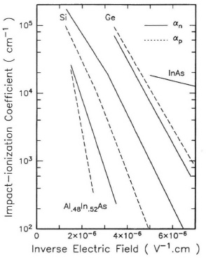
FIGURE 7.3 Impact ionization rate for electrons and holes for Si, Ge, Al0.48In0.52As, and In As (after Tiwari, Ref. 1 © Academic Press).
The condition for breakdown caused by electron-initiated avalanche is the condition where MP goes to infinity. This occurs when the integral in this equality goes to unity. Avalanche breakdown therefore occurs when
The condition for breakdown caused by electron-initiated avalanche can be found following a similar analysis. The expression for the electron multiplication factor is given as
and hence breakdown is said to have occurred when

Note that equations (7.6) and (7.8) are equivalent. The breakdown conditions depend on what is happening in the depletion region and not on the carriers that initiate the avalanche process.
Figure 7.4 shows the avalanche breakdown voltage versus impurity concentration for one-sided abrupt junctions in Si, Ge, GaAs, and GaP. The dashed line indicates the maximum doping beyond which the tunneling mechanism will dominate the voltage breakdown characteristics. The breakdown voltage decreases with increasing impurity concentration. At given doping concentrations, GaP has the highest breakdown voltage, followed by GaAs, Si, and Ge. The avalanche breakdown voltage versus the impurity gradient for linearly graded junctions in Si, Ge, GaAs, and GaP is shown in Fig. 7.5. The dashed line indicates the maximum gradient beyond which the tunneling mechanism will dominate. Again, GaP has the highest breakdown voltage, followed by GaAs, Si, and Ge for given impurity gradients.
7.1.1 Reverse Base Current Phenomenon
In the collector–base depletion region for substantial reverse bias, the electric field intensity is fairly high. Free carriers can be accelerated by the field to a point where they acquire sufficient energy to create additional carriers when collisions occur. If there is a sufficient distance for the carriers to be accelerated to a high-enough velocity, generation of additional carriers during collisions will continue to sustain the avalanche process. Electrons and holes generated in the base–collector space-charge region drift to the quasi-neutral regions under the influence of the electric field. For an n+-p-n-n+ bipolar transistor, impact-ionization-induced electrons are swept to the collector and increase the collector current:
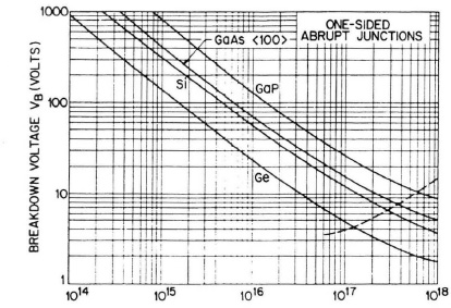
FIGURE 7.4 Collector breakdown voltage versus doping concentration (after Sze, Ref. 2 © John Wiley & Sons).
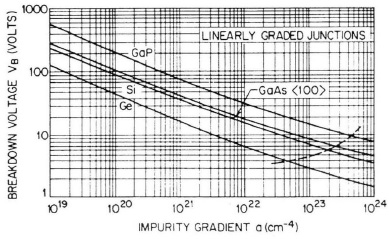
FIGURE 7.5 Collector breakdown voltage versus doping gradient (after Sze, Ref. 2 © John Wiley & Sons).
where ξ is the avalanche multiplication rate (ξ = M − 1) and ![]() is the collector current in the absence of avalanche multiplication.
is the collector current in the absence of avalanche multiplication.
Impact-ionization-induced holes also drift to the quasi-neutral base, as shown in Fig. 7.6. Since the hole current from the base to the emitter is fixed by the base–emitter voltage, excess holes are forced to flow to the base terminal, as shown in Fig. 7.6. The external base current decreases as [3]
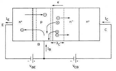
FIGURE 7.6 Hole current flow in avalanche breakdown.
where ![]() is the base current in the absence of avalanche multiplication.
is the base current in the absence of avalanche multiplication.
If the avalanche current ξ IC is larger than ![]() , the terminal current will reverse its sign. However, the base current can be made positive at higher base–emitter bias. This is because the hole diffusion current across the base–emitter junction increases at higher base–emitter bias so that
, the terminal current will reverse its sign. However, the base current can be made positive at higher base–emitter bias. This is because the hole diffusion current across the base–emitter junction increases at higher base–emitter bias so that ![]() is larger than ξ IC. The base–collector avalanche multiplication has strong dependence on the collector current density.
is larger than ξ IC. The base–collector avalanche multiplication has strong dependence on the collector current density.
Avalanche multiplication has strong dependence on the collector current density. The avalanche multiplication rate decreases at higher base–emitter bias because it reduces the electric field in the collector–base depletion region. This is explained as follows. When the collector–base voltage VB E is increased, the electric field in the collector–base space-charge region increases and the space-charge layer expands. The electric field distribution in the bipolar transistor as a function of the collector current for a given VC B is depicted in Fig. 7.7. The peak electric field is located at the collector–base metallurgical junction. From the local field model, the electron and hole impact ionization coefficients are highest at the collector–base metallurgical junction, as evidenced by the impact-ionization-rate plot in Fig. 7.8. When the base–emitter voltage increases, the peak electric field at the collector–base junction decreases gradually, due to electron injection from the emitter (curve 2 in Fig. 7.7). The peak electric field decreases until a uniform distribution is attained (curve 3). At this point, impact ionization at the collector–base junction reaches a minimum. As injection increases further, the peak electric field moves toward the collector region (curve 4). The peak field starts to rise again at higher base–emitter voltages and collector current densities.

FIGURE 7.7 Electric field versus position as a function of collector current density.
When the collector current density approaches the onset current density for the Kirk effect J0, base pushout occurs. The effective base region is then widened and the peak electric field is pushed into the collector high–low junction (curve 5). When JC > J0, the impact ionization rate increases again, due to increases in the peak electric field at the collector high–low junction.
The qualitative explanation of injection-modulated impact ionization is evidenced by the experimental data [4,5], as shown in Fig. 7.9, where the avalanche multiplication rate ξ is extracted by using

FIGURE 7.8 Impact ionization rate versus position from device simulation.
The reverse base current was observed in Si bipolar transistors first [6,7]. A negative base current at a moderate base–emitter bias has also been seen in AlGaAs/GaAs heterojunction bipolar transistors [8]. The physical description of impact ionization in silicon bipolar transistors [9] is suitable for explaining base current reversal in AlGaAs/GaAs heterojunction bipolar transistors. In GaAs heterojunction bipolar transistors, however, the thermal conductivity of the GaAs semi-insulating substrate is low. The AIGaAs/GaAs heterojunction bipolar transistor experiences severe self-heating. Since self-heating increases the junction temperature, avalanche multiplication is reduced.
Figure 7.10 shows the measured collector and base currents versus emitter current for an AlGaAs/GaAs HBT biased at various collector–base voltages. At VC B = 0, impact ionization does not occur and IB is always positive. On increasing VC B and |IE|, the number of electron–hole pairs generated by impact ionization increases. The electrons generated are swept in the collector, contributing a positive term to IC, while the holes generated are collected at the base electrode, contributing a negative term to IB. In particular, at VC B = 6 V this contribution is so high that IB reverses it sign and becomes negative. In general, IB is negative if β(M − 1) > 1. The value of |IE| at which the reversal of IB occurs becomes lower and lower with increasing VC B. On increasing |IE| further, different effects contribute to a decrease in the generation rate and IB recovers to a positive value, as occurs for |IE| > 10 mA at VC B = 8.6 V (see Fig. 7.10). These effects are voltage drops due to RC and RB parasitic resistances, device self-heating, and electric field lowering in the base–collector junction due to the presence of mobile carriers. Figure 7.11 shows the effect of reducing device self-heating by pulsing IE with a duty cycle as low as 0.2% and correcting voltage drops on parasitic resistances (the extracted values being RB = 180 Ω, RC = 10 Ω) [10]. At a given |IE| in Fig. 7.11, the difference between dc and pulsed response is caused by the self-heating effect. The effect of parasitic resistances on the avalanche multiplication factor is seen by the pulsed curves with and without RB and RC correction.

FIGURE 7.9 Impact ionization versus collector current (after Liu et al., Ref. 5 © IEEE).

FIGURE 7.10 Gummel plot of an AlGaAs/GaAs HBT (after Zanoni et al., Ref. 8 © IEEE).

FIGURE 7.11 Self-heating effect on ionization multiplication factor (after Zanoni et al., Ref. 8 © IEEE).
7.1.2 Nonlocal Avalanche Effect
The collector doping profile directly influences impact-ionization effects and breakdown voltage, which are important factors for power applications of HBTs. High-speed performance and breakdown voltage cannot be optimized independently. Due to the strong electric fields present in the base–collector space-charge region of HBTs and to the presence of hot electron phenomena, conventional drift-diffusion analysis, which assumes locality of ionization events, is inadequate to describe and predict the avalanche breakdown. The local model implies that the impactionization coefficients at the base–collector metallurgical junction are the highest. Since electrons must travel a nonnegligible distance within the collector before attaining sufficient energy to initiate impact ionization, ionization events do not occur in correspondence to maximum electric field. Such a phenomenon is referred to as a nonlocal or dead-space effect [11] since the electron energy usually lags the electric field. For an n-p-n bipolar transistor, the peak electron impact-ionization coefficient shifts from the base–collector metallurgical junction into the collector, and the peak hole impact-ionization coefficient shifts from the base–collector metallurgical junction into the base, as evidenced by Monte Carlo simulations [10]. The local electric field model thus overestimates the avalanche multiplication rate compared to that obtained from the energy model, which uses mean carrier energy. Furthermore, as the collector–base voltage approaches the breakdown voltage, the contribution of secondary holes must be accounted for. Experimentally, the secondary holes cause a steep increase in the avalanche rate at a peak electric field of 9 × 10⁵ V/cm [11, 12].
The nonlocal model for impact-ionization current may be implemented as follows [13]. For a given E(x) in the collector–base depletion region, the electron temperature Te(x) can be approximated by [14]
where λe is the energy relaxation length of the electron. The solution of the equation is given by
For an abrupt n-p junction with uniform doping concentration in the quasi-neutral regions,

where x = 0 is at the edge of the depletion layer next to the quasi-neutral n region, x = xa is at the metallurgical junction, and x = xb is at the edge of the depletion layer next to the quasi-neutral p region. Inserting the electric field into (7.13) gives
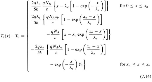
where
![]()
For x > xb,
where

A graphical representation of the normalized electric field and the electron temperature distributions is displayed in Fig. 7.12. The solid lines in this figure represent the nonlocal model and the dashed lines represent the local model. It is clear from this plot that the nonlocal model shows the energy lag effect. Figure 7.13 shows experimental data for M − 1 obtained at |IE| = 50 nA compared with values calculated by the local model and the energy model with and without the contribution of secondary holes to ionization. In the local model, αn, p(E(x)) is modeled as αn, p exp[−βn, p/ E(x)]. In Fig. 7.13, αn = 5 × 106 cm−1 and βn = 1.6 × 10⁶ V/cm. When holes are considered (dashed lines in Fig. 7.13), αp = 1.01 × 106 cm−1 and βp = 2.11 × 10⁶ V/cm. For the energy model, λe = 70 nm and λh = 100 nm. At low VC B the simulated curves with and without the contribution of holes are superimposed. The inclusion of secondary holes gives more accurate M − 1 predictions at high VC B. To improve the predictability of the avalanche multiplication model at very high electric field intensity, incorporation of a delay in the conventional current equation has been proposed [11]. This simple analytical approach provides a steep increase in the avalanche multiplication rate for ξ > 10.

FIGURE 7.12 Normalized electron temperature and field distributions in the collector (after Hong and Fossum, Ref. 13 © IEEE).
The multiplication factor is defined by the ratio of electron current density Jn (xb) where electrons enter the space-charge region to Jn (0), where electrons leave the space-charge region:
To model the avalanche current correctly, the impact-ionization rate as a function of electron temperature must be used. For example,

FIGURE 7.13 Comparison of local and nonlocal model in impact ionization characteristics (after Zanoni et al., Ref. 12 © IEEE).
where A0 and β0 are impact ionization coefficients and Te(x) is given in (7.14) and (7.15)
7.1.3 Influence of the Base Thickness on the Collector Breakdown
When the base thickness is less than the electron mean free path, electrons enter the collector region with excess energy and initiate impact ionization after acquiring additional kinetic energy from the electric field. Figure 7.14 illustrates the energy-band diagram of an AlIn As/InGaAs HBT showing the collector impact ionization caused by high-energy injection from the emitter under nonequilibrium transport. In the impact-ionization process, an energetic electron undergoes a transition to a lower state, during which another electron is excited across the bandgap.
A key to understanding the effect of high-energy injection from the emitter and ballistic base transport on impact ionization in the collector is the threshold energy for electron-induced impact ionization. The threshold energy can be calculated from knowledge of energy-band structures. For example, consider an initial electron in a conduction-band with a wave vector ki making a transition to a lower state with a wave vector k1. This will then excite an electron from a state at k2 in the valence band to k3 in the conduction-band. Conservation of total energy and momentum together with the condition for minimum energy requires that at threshold
where vgi = 2π/h∇k E (ki) is the group velocity of a charge carrier with a wave vector ki. Using the condition in (7.18) with the method of Anderson and Crowell [16], the threshold for impact ionization along the direction of electron transport in the collector occurs for an electron with Ei = 0.83 eV above the conduction-band minium.

FIGURE 7.14 Energy-band diagram of an AlInAs/InGaAs HBT (after Jalali et al., Ref. 15 © IEEE).
Comparison of the collector ionization threshold Ei = 0.83 eV and the emitter injection energy E0 = 0.48 eV indicates that hot electron injection enhances impact ionization in the collector if electrons traverse the base before dissipating their energy via inelastic collisions. Figure 7.15 shows the measured multiplication factor using (7.11) for AlInAs/InGaAs transistors with a base thickness of 200, 400, 700, 1200, and 4000 Å. The common-base breakdown voltage is BVC B0 6.5 V for all devices. High collector–base junction breakdown is desirable for high device linearity and high-power application. The breakdown voltage is governed by the collector doping and width because the base is highly doped. Thicker and lower-doped collectors increase the breakdown voltage at the expense of increased collector depletion-layer transit time. The collector–emitter breakdown voltage is governed by collector–base breakdown coupled with a feedback multiplication factor of the current gain. BVC B0 is related to BVC E0 as follows:
where n is an empirical constant between 2 and 6. In Fig. 7.15 the base–emitter voltage is kept the same for all measurements to ensure the same injection energy. In the thin base region, charge transport can be described by ballistic or quasiballistic motion. The multiplication factor has been increased significantly.
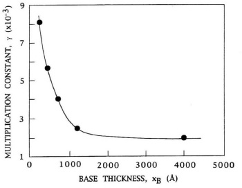
FIGURE 7.15 Measured multiplication factor versus base thickness (after Jalali et al., Ref. 15 © IEEE).
Since the base and collector transport are coupled, there is a trade-off between the need for short base and collector transit times and adequate collector breakdown voltage. This is more important for AlInAs emitter HBTs than those with InP emitters because of the 0.48-eV injection energy compared to 0.24 eV for the latter. The optimum base design must result in a small intrinsic delay with reasonable transistor output impedance.
7.1.4 Avalanche Effect on the Collector-Base Junction Capacitance
The free carrier capacitance concept has been applied to the collector–base junction capacitance where free carriers in the collector–base depletion region are injected from the emitter. For silicon bipolar transistors, free carrier capacitance becomes important when base pushout occurs. For GaAs heterojunction bipolar transistors, base pushout is suppressed due to high collector doping and valence-band discontinuity at the collector–base heterojunction. However, free carriers generated by avalanche multiplication can become important. The collector–base junction capacitance of the HBT, including the impact-ionization effect, is written as [17]
where ΔQp is the hole mobile charge in the collector–base depletion region(ΔQp = ΔQn).
For an N-p-n heterojunction bipolar transistor, impact-ionization-induced electrons in the collector depletion region are swept to the collector and impact-ionization-induced holes drift to the base terminal. The ionization-induced hole charge is associated with the incremental base current density Δ JB [= (M − 1) JC] and can be expressed by using the charge-control model:
where τ is the lifetime and
Using (7.21) and (7.22), the free carrier capacitance per unit area due to impact ionization is expressed as
Since the Early voltage of the heterojunction bipolar transistor is very large, the base-width modulation effect on the collector current ∂JC/∂VBC is very small. For an injection-level independent lifetime, (7.23) is approximated as

The analytical prediction of collector–base junction capacitance including avalanche effect is compared against MEDICI simulation. The Al1−x GaxAs/GaAs heterojunction bipolar transistor has an abrupt emitter–base heterojunction with an aluminum mole fraction x = 0.3, emitter doping 2 × 1017 cm−3, base doping 1019 cm−3, collector doping 1 × 1017 cm−3, emitter thickness 0.1 μm, base thickness 0.1 μm, and collector thickness 0.6 μm. The physical models used in MEDICI include Shockley–Read–Hall recombination, Auger recombination, bandgap narrowing, impact ionization, and concentration-and field-dependent mobilities. Figure 7.16 shows the electron and hole concentrations in the collector obtained from MEDICI for the HBT at VB E = 1.4 V and VC B = 6 and 12 V. The electron and hole concentration and depletion region thickness at VC B = 12 V are much larger than those at VC B = 6 V. The difference is obviously due to avalanche multiplication at the large reverse-biased junction. Impact-ionization-induced holes drift to the base terminal, which reduce the base current at high VC B, as shown in Fig. 7.17. In this plot the line represents the model prediction using (7.10) and the squares represent the MEDICI simulation results. The agreement between the model predictions and simulation data is excellent. The agreement allows us to obtain empirical parameters B VC B0 and n accurately. From the base current, BVC B0(= 13 V) and n(= 1.4) are extracted and then used to predict the collector–base junction capacitance at high collector–base bias. The results are illustrated in Fig. 7.18. The collector–base junction capacitance decreases with collector–base voltage and then increases with VC B when the device is in close proximity to avalanche breakdown. An abrupt increase of the collector junction capacitance at VC B > 12 V is seen in Fig. 7.18, which is consistent with base current reversal when VC B is approaching B VC B0.

FIGURE 7.16 Electron and hole concentrations in the collector (after Yuan and Ning, Ref. 17 © Elsevier Science).
7.1.5 Avalanche Effect on the Output Conductance
Avalanche multiplication also changes the output conductance of the HBT. The output conductance of the bipolar transistor is defined as

FIGURE 7.17 Base current versus collector–base voltage (after Yuan and Ning, Ref. 17 © Elsevier Science).
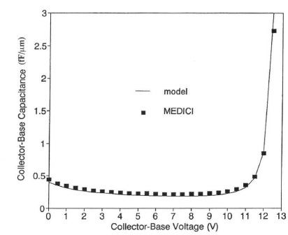
FIGURE 7.18 collector–base junction capacitance versus collector–base voltage (after Yuan and Ning, Ref. 17 © Elsevier Science).
Using (7.9) and (7.22), the output conductance per unit area is derived as

7.1.6 Breakdown and Speed Considerations in lnGaAs HBTs
In the III/V compound heterojunction bipolar transistors, AlGaAs/GaAs and AlInAs/GaInAs HBTs exhibit different temperature behavior in collector breakdown voltage [18]. Figure 7.19 shows the common-emitter I−V characteristics at 25 and 125°C for the GaAs and In0.53Ga0.47 As HBTs. The de current gains are β (GaAs) = 60 and β(In0.53Ga0.47As) = 130 for IC = 1 mA. It is evident that there are significant differences in the I−V characteristics of the transistors. For the GaAs HBT, the collector current saturates completely with negligible output conductance. The collector breakdown voltage BVCEX is greater than 10 V at 25°C and actually increases at 125°C. In contrast, the In0.53Ga0.47As HBT has poor saturation characteristics with high output conductance. The collector breakdown voltage, BVCEX, is very low, less than 2.5 V at 25°C, which is related to the high current gain in the transistor. The collector breakdown voltage is also seen to decrease at 125°C. The poor saturation characteristics and low collector breakdown voltages in the ln0.53Ga0.47As collector are caused by thermally generated leakage current at the collector–base junction.
It has been noted by many researchers that InGaAs-collector HBTs grown on InP substrates exhibit low common-emitter collector breakdown BVCEO and high output conductance [18,19]. This is believed to be related to the low bandgap in the InGaAs collector. The use of δ-doping techniques for the improvement of breakdown characteristics [20] may not be applicable to the InP/InGaAs due to the high electric fields associated with δn+ or δp+ layers. Although the collector–base breakdown voltage increases with collector thickness, the collector transit time becomes larger in this case and degrades the overall speed performance. To increase the collector breakdown voltage, the use of InP rather than InGaAs collectors is attractive. InP has a larger bandgap energy (1.35 eV) and greater saturation velocity (1.3 × 107 cm/s) than InGaAs. The conduction spike at the collector–base heterojunction, however, tends to degrade the electron transport.
The study of breakdown–speed characteristics has been carried out using single and double heterostructures with InGaAs and InP collectors [21]. The design of different-collector HBTs is shown in Fig. 7.20. The thickness, doping, and composition of the emitter, base, and subcollector are kept the same for all designs in order to have a fair comparison. All collectors have a thickness of 3000 Å and are either doped at 5 × 1016 cm−3 or left undoped. For single HBTs, the InGaAs collectors are chosen based on (A)n−, (B) p−, (C)i, and (D)p− -n− design schemes. The first three structures correspond to the conventional, inverted field, and modified (without δp+ toward the subcollector side) undoped collector designs. Design (E) uses a wider bandgap InP collector to improve the breakdown characteristics. This collector results in a double heterojunction with an abrupt transition from the InGaAs base to the InP collector.

FIGURE 7.19 Collector current versus collector–emitter voltage for (a) GaAs and (b) InP HBTs (after Malik et al., Ref. 18 © IEEE).
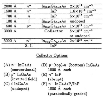
FIGURE 7.20 Design of different-collector HBTs (after Chau et al., Ref. 21 © IEEE).
The base–collector heterojunction spike can be smoothed out by using composition grading in design (F), where a parabolically graded profile is used.
The collector breakdown voltage BVC B0 of InP/InGaAs single HBTs as a function of collector current density is depicted in Fig. 7.21. The breakdown voltage was obtained from one-dimensional device simulation. The simulation results underestimate the breakdown characteristics compared to the experimental data. However, the expected trends of the simulation results are correct and therefore serve as guidelines for comparing the relative performance of various designs rather than estimating the absolute values of the breakdown voltages. In Fig. 7.21 the breakdown voltage is highest for doping profile (C) and smallest for (A) and (B) at low current densities. At high collector current densities, devices (B), (C), and (D) show monotonic decrease in BVC B0 with JC whereas device (A) shows a peak in the breakdown voltage–JC characteristics. This makes BVC B0 of device (A) larger than the other three devices at high JC. The difference arises because of the change in the peak electric field with current. In the n− collector (A), Epeak occurs at the base–collector interface, whereas in (B) and (C), it occurs at the collector–subcollector interface. Since high injection at the collector changes the position and magnitude of Epeak in design (A), the breakdown voltage increases with JC initially and then decreases rapidly at high collector current densities. In the case of p− and i collectors, Epeak always occurs at the collector–subcollector interface, resulting in a rapid decrease of BVC B0 with JC under all current-level injections.

FIGURE 7.21 Base–collector breakdown voltage versus collector current (after Chau et al., Ref. 21 © IEEE).
Figure 7.22 shows the sum of the base transit time and the collector space-charge layer transit time of the four HBTs as a function of collector current density. The p−collector (device B) has the shortest total transit time followed by i (C), p− -n− (D), and n− (A) collector devices. Device A is the slowest due to the high electric field at the base end of the collector SCR region which results in electron excitation to the upper energy valleys. The other three HBTs [devices (B), (C), and (D)] all show broad velocity overshoot characteristics, which give rise to shorter transit time. The figure of merit
VC B| JB=0/ (τB + τSCR)|VC E=VC E.br/2
is plotted as a function of collector current density in Fig. 7.23. The figure of merit for all four devices decreases with the collector current density. Among the four HBTs, the i-collector design (C) has the highest breakdown voltage and the p− -collector design (B) has the shortest total transit time. In terms of speed–breakdown tradeoffs, the results of Fig. 7.23 show that p− -n− collectors have the best performance, while design p− has the worst performance. Thus optimum collector designs such as (B), which normally give the highest speed, do not necessarily combine good power characteristics.

FIGURE 7.22 τB + τSC R versus collector current density (after Chau et al., Ref. 21 © IEEE).

FIGURE 7.23 Figure of merit versus collector current density (after Chau et al., Ref. 21 © IEEE).
7.2 THERMAL INSTABILITY
A three-dimensional transmission-line matrix simulation was used to evaluate the thermal behavior of power HBTs with multiple emitter fingers [22]. The power device consists of five cells. Each cell has two emitter fingers grouped closely together by the emitter–base self-alignment process. The temperature distribution at a dissipated power density of 2 mW/μm2 under steady state is simulated. Figure 7.24a shows the isometric view of the temperature distribution of five emitter fingers and Fig. 7.24b is the contour plot with intervals of 15°C. The isometric projection and the corresponding temperature contours clearly display that two peak values of the junction temperature occur at the centers of the two central emitter fingers. The junction temperature drops sharply around the central cell, with an average temperature gradient of as high as 9°C/μm in these areas. From a device-reliability point of view, the peak junction temperature is the most important parameter for the device thermal design and should be used to characterize the device thermal behavior.
Despite the fact that the multifinger HBT has become increasingly important and popular in high-power microwave applications, efforts to model such a device analytically have been limited due to the complicated nature of thermal coupling between the neighboring emitter fingers. Consider a three-finger-pattern HBT. The temperature of the two outer fingers, which have identical thermal properties due to the symmetrical geometry, and the temperature at the center finger are given by

FIGURE 7.24 (a) Isothermal and (b) contour plot of a five-finger HBT (after Gui et al., Ref. 22 © IEEE).
where the subscripts S and C denote outer and center fingers, respectively. Rth is the thermal resistance due to self-heating in the unit HBT, and Rcp is the thermal resistance due to heating from the neighbor emitter elements.
Rth can be determined using (3.45). The value of Rcp depends on the geometry of the emitter fingers and the process including the emitter mesa etching and metallization. For typical mesa-etch HBTs, Rcp has been determined empirically as
where δ is a fitting parameter with a typical value of 0.25, and Sf is the emitter-finger spacing in μm. Decreasing Sf will increase Rcp.
7.2.1 Emitter Collapse Phenomenon
Power heterojunction bipolar transistors are designed to deliver large amounts of power at high frequencies. Because these HBTs are operated at high power densities, the ultimate limit on their performance is imposed by thermal considerations. Recently, a thermal phenomenon was observed for the case when a multifinger GaAs HBT was operating at high power densities [23]. This phenomenon, referred to as emitter collapse, occurs when one finger of a multifinger HBT suddenly conducts most of the device current. This leads to an abrupt decrease in current gain. The collapse does not cause the HBTs to fail immediately, and the device can be biased in and out of the collapse by adjusting the level of power dissipation. This collapse, however, degrades the device performance significantly and should be avoided.
The collapse phenomenon is illustrated by the common-emitter I−V characteristics measured at constant base currents. As the collector–emitter voltage increases, the power dissipation in the HBT increases. This increase in power dissipation elevates the junction temperature above the ambient temperature and causes an increase in base and collector currents. At high VC E, impact ionization increases IC. At a certain collector–emitter bias, the collapse of collector current occurs, as shown in Fig. 7.25. At an even higher collector–emitter voltage, the collector current goes to infinity due to the domination of avalanche breakdown again.
Consider the case of a multifinger HBT. If one finger becomes slightly warmer than the others, this particular finger conducts more current at a given base–emitter bias. This increased collector current, in turn, increases the power dissipation in the junction and raises the junction temperature and collector current even further. The collapse occurs when the junction temperature in one finger becomes much hotter than the rest of the fingers.
Note that the collapse does not cause the HBTs to fail immediately. In fact, the collapse is reversible and the same device can be measured for several experiments. This is markedly different from thermal runaway in silicon BJTs, which causes the devices to fail irreversibly. Both thermal runaway in BJTs and the collapse of HBTs result from an increase in junction temperature. Since the current gain in Si bipolar transistors increases rather than decreases with temperature, the increased current in that finger of the BJT will draw more and more current. This is in contrast to the collapse when IC decreases after the critical condition occurs.

FIGURE 7.25 Collector current versus collector-emitter voltage (collapse phenomenon).
The collector current collapse (or crush) effect has also been observed by using numerical electrothermal simulation [24]. The contour plots of the temperature distribution on the top surface of a three-finger HBT under the bias of VCE = 2, 3, 5, and 6 V are shown in Fig. 7.26. The first two operation points are before the current crush. At this point the temperature variation is small across the three emitter fingers. The last two operating points occur after the current crush. The temperature distribution here shows a drastic difference between the center and the other two emitter fingers. As VCE increases, the center finger will eventually conduct the largest base current, and the other two fingers become nearly inactive. The collector current wi ll continue to decrease due to the smaller current gain at higher junction temperatures.
7.2.2 Relation Between Emitter Collapse and Avalanche Breakdown
The interdependence between collapse phenomenon and avalanche breakdown is discussed in detail in this section. The measured and calculated I–V characteristics for IB = 5 μA are shown in Fig. 7.27. The calculated collector current of a six-finger HBT flowing in the hot finger is IC1 and in one of the cold fingers is IC2. The calculated total current is IC1 + 5IC2. Significant avalanche multiplication starts at VCE ≈ 22.5 V for both curves. The collector current reaches a maximum value of 5.3 mA before the collapse occurs and the collector current decreases. In Fig. 7.27, at point A, which corresponds to VCE ≈ 22.5 V and IC ≈ 0 A, the collector current level is well below the collapse locus. Therefore, the total device current at point A is uniformly distributed among the six fingers. As VCE increases slightly past point A, impact ionization in the base–collector junction becomes noticeable. The product of the avalanche multiplication factor Mn and the current transfer ratio α0 approaches unity, and causes the collector current to increase rapidly toward the collapse locus. This well-known trend of increasing IC, however, stops abruptly upon initiation of the collapse at point B, corresponding to VCE ≈ 24.1 V. Beyond this point, a further increase in collector–emitter voltage results in a greater proportion of the collector current being conducted in the hot finger, until all of the available device current is conducted through the hot finger.

FIGURE 7.26 Contour plot of temperature distribution for (a) VCE = 2 V, (b) VCE = 3 V, (c) VCE = 5 V, and (d) VCE = 6 V (after Liou and Bayraktaroglu, Ref. 24 © IEEE).
Between point B, which marks the onset of the collapse, and point D, where the device bums out, device operation can be separated into two phases according to the features in the junction temperature of the hot finger (T1). Between points B and C, T1 quickly increases toward some drastically higher temperature than that prior to collapse. The rapid increase of T1 in the hot finger corresponds to the rapid decrease of T2 in the cold finger. During this phase, the incremental increase of IC1 with respect to VCE is high since a greater amount of current flows into the hot finger. The surge in power density further increases the hot finger junction temperature. In contrast, the cold finger loses more and more of its current with increasing VCE and the cold finger temperature plummets. Between points C and D, most of the available current has been directed to the hot finger. The six-finger HBT is effectively a one-finger HBT, with the hot finger conducting the entire device current.

FIGURE 7.27 Measured and calculated I–V characteristics (after Liu, Ref. 25 ©IEEE).
The classification of the two distinct phases in the T1 characteristics is critical to the understanding of the collapse–avalanche breakdown interaction. Figure 7.28 shows both electron ionization multiplication factor Mn and zero-ionization current gain β0 as a function of VCE. The two phase boundaries are marked in Fig. 7.28 as dashed lines. All six fingers share current equally before phase I. Hence Mn and β0 of the six fingers are indistinguishable. In phase I, when the current redistributes among the fingers, T1 increases dramatically while T2 decreases toward room temperature. Because in general both Mn and β0 decrease with temperature, Mn1 and β01of the hot finger decrease from their values prior to phase I. In contrast, Mn2 and β02 of the cold fingers increase with VCE because the cold finger temperature decreases. In phase II, T1 remains relatively constant and T2 continues to decrease slowly toward room temperature. Because T2 no longer increases dramatically, Mn1 reverses its decreasing trend and increases gradually with VCE because of the increased ionization rate with higher electric field. Similarly, β01 no longer decreases dramatically with VCE but stays relatively constant. Meanwhile, Mn2 and β2 continue to increase, as in phase I.
7.2.3 lnP HBT Thermal Instability
For AlGaAs/GaAs heterojunction bipolar transistors, the collapse of current gain occurs when the thermal instability condition is met. Because the current gain decreases with temperature in the AlGaAs/GaAs HBT, the increasing junction temperature during thermal instability causes the current gain to decrease dramatically leading to the collapse. For InP heterojunction bipolar transistors, the current gain is essentially independent of the junction temperature. Therefore, further examination is required to see how the InP HBT characteristics are modified upon entering the thermal instability condition.

FIGURE 7.28 Calculated (a) junction temperature and (b) electron ionization multiplication factor and current gain as a function of VCE (after Liu, Ref. 25 © IEEE).
Figure 7.29 shows the measured I–V characteristics of a two-finger InP HBT. Each finger has an area of 2 × I 0 μm2. The total collector current of these two fingers is plotted against VCE as a function of the total base current from 0.07, 0.24, 0.44, 0.56, 0.66, 0. 76, 0.86 to I mA. The emitter resistance is measured to be 8 Ω per finger. The familiar decrease of IC with VCE appears only at high current levels in the region marked A in Fig. 7.29. At medium current levels (region B), the collector current increases abruptly at certain values of VCE, opposite to what is observed in region A. At low current levels, the collector current increases toward infinity similarly to the breakdown mechanism.

FIGURE 7.29 Measured I–V characteristics of a two-finger InP HBT (after Liu et al., Ref. 26 © IEEE).
Figure 7.30 displays the individual collector currents corresponding to the Ic–VCE plot in Fig. 7.29. The dashed and dotted lines in Fig. 7.30 represent the hot finger and cold finger, respectively. In contrast to Fig. 7.25, the individual currents clearly demonstrate that thermal instability occurs at some bias conditions in all three regions. Before the thermal instability loci, both fingers conduct relatively identical currents. Beyond the instability loci, a current and junction temperature increase in the hot finger occurs. When the hot finger takes away the cold finger current, the hot-finger current gain decreases, resulting in the collapse of the overall collector current. The collapse observed in a multifinger InP HBT is in principle similar to that in the AlGaAs/GaAs HBT. The major difference is that the gain collapses in the InP HBT are due to its current gain dependence on collector current, while the gain collapses in the AlGaAs HBT are due to its current gain dependence on temperature. Therefore, the collapse in the AlGaAs/GaAs HBT occurs over the entire range of current levels and the collapse in the InP HBT occurs only at high current levels.

FIGURE 7.30 Individual collector current corresponding to the I–V of Fig. 7.29 (after Liu et al., Ref. 26 © IEEE).
7.2.4 Modeling the Emitter Collapse Loci
The critical current level at the collapse loci separating the normal region and the collapse region is modeled as [27]

where N is the number of emitter fingers and ![]() is the base–emitter junction voltage feedback coefficient.
is the base–emitter junction voltage feedback coefficient.
Figure 7.31 plots the collapse loci of the I–V characteristics at the four substrate temperatures. In this figure, solid lines represent the measured collapse loci and the dashed lines are the calculated collapse loci. The temperature dependence of all the parameters was evaluated. The ideality factor nf of the collector currents are 1.165, 1.110, 1.070, and 1.041 as TA increases from 25, 100, 175, and 250°C, respectively. The emitter resistances measured with an open-collector method [28] are found to be 4.0 Ω per finger throughout the various ambient temperatures. The thermal-voltage feedback coefficients are determined by measuring the base–emitter turn-on voltage at Ic = 60 mA at various substrate temperatures between 25 and 300°C. The base–collector bias was maintained at 0 V during such measurements, so that the actual junction temperature was well approximated by the substrate temperature. Similar to the emitter resistance, ![]() does not vary with ambient temperature, remaining roughly at 1.0 m V/°C. Among all the parameters, the thermal resistance is the one that manifests the strongest dependence on TA. The thermal resistance per finger, estimated from measurements, is found to be 930, 1050, 1200, and 1370°C/W as TA increases from 25, 100, 175, and 250°C, respectively. The increase in thermal resistance with respect to TA is caused by the reduction of the GaAs thermal conductivity at higher temperatures. As seen in Fig. 7.31, the model predictions are in good agreement with the experimental data. Equation (7 .30) is generally correct and applicable at various elevated temperatures.
does not vary with ambient temperature, remaining roughly at 1.0 m V/°C. Among all the parameters, the thermal resistance is the one that manifests the strongest dependence on TA. The thermal resistance per finger, estimated from measurements, is found to be 930, 1050, 1200, and 1370°C/W as TA increases from 25, 100, 175, and 250°C, respectively. The increase in thermal resistance with respect to TA is caused by the reduction of the GaAs thermal conductivity at higher temperatures. As seen in Fig. 7.31, the model predictions are in good agreement with the experimental data. Equation (7 .30) is generally correct and applicable at various elevated temperatures.

FIGURE 7.31 Collapse loci at the four different substrate temperatures (after Liu and Khatibzadeh, Ref. 27 © IEEE).
The thermal instability criterion is the S-factor proposed for silicon bipolar transistors [29]. The S-factor is given by
The transistor is said to be thermally unstable when S > 1. From the plot of collector current versus junction temperature rise, the S-factor can be plotted. Figure 7.32 shows the S-factor as a function of junction temperature rise at different base–emitter voltages. The curve connecting the points where S = 1 is the S-factor loci. Note that in practice S-factor values obtained are very close to, but not exactly equal to, unity. Thus the S-factor loci are the points having the highest S-factor values. In fact, the collapse loci and the S-factor loci are governed by the same equation, namely, (7.31).
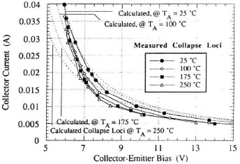
FIGURE 7.32 S-factor versus junction temperature (after Liu and Khatibzadeh, Ref. 27 ©IEEE).
For the S-factor loci, one can write
Taking the derivative of (7.32) with respect to T, we have
where β* is the coefficient that measures the amount of bandgap shrinkage as T increases. Solving for ∂IC/∂T and setting S = 1, one then deduces the same equation for the S-factor loci as (7.31).
If the temperature variation of Rth is considered, the S-factor defined in (7.31) should be revised as

From (7.34) the governing equation of the collapse loci, taking into account the Rth variation with temperature, can be derived:
7.3 DESIGN IN THERMAL STABILITY
7.3.1 Emitter Ballasting Resistors
To reduce the likelihood of the emitter collapse phenomenon, and to ensure a more uniform current distribution, emitter ballasting (EB) resistors can be inserted in series with each emitter finger. However, the determination of the value of ballasting resistance is not simple. There are a number of conflicting requirements. Too large a resistance will cause degradation of power gain while too small a resistance will not effectively protect the HBT from thermal instability. The optimal value of the total ballasting resistance is determined by [30]
where RT is the total thermal resistance from the active device area to the point where the case temperature Tc is measured, Tj = IC VCE RT + Tc, REC is the emitter contact resistance, ![]() and
and ![]()

FIGURE 7.33 Junction temperature for various emitter ballasting resistors (after Gao et al., Ref. 30 © IEEE).
The effect of the emitter ballasting resistors on the junction temperature of the AlGaAs/GaAs HBT is shown in Fig. 7.33. In the figure, curve 1 represents the HBT without ballasting resistors, curve 2 represents the HBT with equally valued emitter ballasting resistors, and curve 3 represents the HBT with unequally valued emitter ballasting resistors. As seen in Fig. 7.33, the nonuniform junction temperature distribution with multiple emitter fingers over the entire active region can be improved by using ballasting resistors, especially unequally valued emitter resistors. It is anticipated that highly thermostable HBTs with homogeneous junction temperature can be fabricated by this technique.
The effects of emitter-finger layout, emitter resistance, and substrate thermal conductivity on collector current crush are also demonstrated by the numerical simulation results [25]. The dependence of current instability on the spacing between emitter fingers is shown in Fig. 7 .34a. The maximum temperature on the chip as a function of VCE is also given. The case of zero spacing corresponds to an HBT with only one emitter finger with an area of 10 × 6 μm2. As the spacing between the emitter fingers increases, VCE shifts slightly to a smaller value, while IC shifts slightly to a larger value, at the current crush point. This result shows that the threshold power current instability is only rrunimally improved by increasing the emitter-finger spacing beyond 10 μm and not increasing the number of emitter fingers. The dependence of current crush due to thermal instability on the emitter specific resistance is shown in Fig. 7.34b. As the emitter specific resistivity ρe increases, threshold power increases. This result verifies the reduction in thermal instability by implementing a ballast resistor at each emitter node. The dependence of current crush on the substrate thermal conductivity is shown in Fig. 7.34c. A reduction in the thermal resistance due to an increase in the thermal conductivity results in a smaller temperature rise and a larger critical voltage for current crush. Improvement in thermal instability by increasing substrate conductivity is the most efficient way of increasing power capability without encountering high-frequency limitations and consuming extra semiconductor area. This suggests that the power HBT on Si substrate provides a smaller negative differential resistance and a larger current crush voltage and is more thermally stable than the HBT on GaAs substrate. verifies the reduction in thermal instability by implementing a ballast resistor at each emitter node. The dependence of current crush on the substrate thermal conductivity is shown in Fig. 7.34c. A reduction in the thermal resistance due to an increase in the thermal conductivity results in a smaller temperature rise and a larger critical voltage for current crush. Improvement in thermal instability by increasing substrate conductivity is the most efficient way of increasing power capability without encountering high-frequency limitations and consuming extra semiconductor area. This suggests that the power HBT on Si substrate provides a smaller negative differential resistance and a larger current crush voltage and is more thermally stable than the HBT on GaAs substrate.

FIGURE 7.34 Ic–VCE for various (a) emitter resistivities, (b) spacing, and (c) substrate conductivities (after Liou and Bayralktaroglu, Ref. 24 © IEEE).
7.3.2 Emitter Thermal Shunt
Recently developed thermal shunt technology [31, 32] has the benefit of improving the thermal stability of the HBT while the device cutoff frequency and efficiency are not reduced. Thermal-shunted HBTs utilize a thermal stabilization feature to minimize problems due to nonuniform junction temperature distribution, without the addition of ballast resistors. In thermal-shunted devices, the emitter elements are connected by a thick metal bridge (thermal shunt). Temperature differences between emitter elements are reduced since the emitters are now thermally coupled to each other. To reduce temperature nonuniformities efficiently, the thermal shunt thickness needs to be larger than 10 μm, which is significantly larger than the conventional emitter metallization thickness. In addition, the shunt channels transfer heat to spreading areas on the substrate that further lowers the thermal resistance compared to conventional device geometries. The heat-spread areas are referred to as thermal lenses. Figure 7.35 shows a typical layout for a thermally shunted device. The thermal lenses are the areas of the thermal shunts that anchor onto the emitter pads. Bar shaped emitter elements (device B 1) are shown in Fig. 7.35a and dot-shaped emitter elements (device Dl) are displayed in Fig. 7.35b. Device Bl has five bar-shaped emitter elements. Each element is a 3-μm x 11.8-μm rectangle which is surrounded by a self-aligned base finger that leads to the base pad. The base fingers are separated by 24 μm (edge to edge). The collector is interdigitated between the base fingers. Device D1 has 25 dot-shaped emitter elements. Each row of five dots is surrounded by a self-aligned base finger that leads to the base probe pad. Dots in each base finger are 3 μm in diameter and are separated by 6 μm (edge to edge). The D1 device has a wider thermal shunt than that of the B 1 device, due to dot spacing requirements. The total emitter area of both devices is 177 μm2. A summary of the geometries of the two devices and their thermal resistances at different power dissipations is given in Table 6.1.
Figure 7.36 shows the collector current versus the collector–emitter voltage of device D1 measured at room temperature. The negative differential resistance in the forward active mode is due to self-heating. Current collapse in a nonthermal shunt device occurs at a power density of about 1.33 mW/μm2 [27], while the thermallyshunted devices have been taken up to a power density of 3.50 mW/μm2 without showing signs of current collapse. The measured cutoff frequencies are between 50 and 60 GHz and fmax between 85 and 100 GHz. These results compare favorably with those of the non-thermal-shunt device, suggesting that the extra parasitic reactance elements due to the thermal shunt are not significant.

FIGURE 7.35 Layouts for (a) an emitter-bar device and (b) an emitter-dot device (after Sewell et al., Ref. 32 © IEEE).
Figure 7.37 shows the junction temperature and extrapolated thermal resistance versus power for bar-shaped emitter and dot-shaped emitter HBTs. The increase in thermal resistance at higher power densities is due to the temperature-dependent thermal conductivity of the GaAs substrate. The dot-shaped emitter devices have smaller thermal resistances and junction temperatures than those of the bar-shaped emitter devices over a wide range of power. The lower thermal resistance for the DI device is due primarily to the spreading of the heat sources and the larger thermal shunt width. At a power of 0.1 W, thermal resistance is 147 and 232°C/W for DI and B1 devices, respectively. For a conventional HBT without thermal shunt, thermal resistances of 465°C/W (120 μm2 emitter area) [27], l000°C/W (60 μm2 emitter area) [33], and 1500 °C/W (41 μm2 emitter area) [34] have been reported at 0.1 W.

FIGURE 7.36 Collector current versus collector–emitter voltage (after Sewell et al., Ref. 32 © IEEE).

FIGURE 7.37 Junction temperature and thermal resistance versus power (after Sewell et al., Ref. 32 © IEEE).
7.3.3 Base Ballasting Resistors
The use of emitter ballasting resistors is somewhat effective to prevent the collapse of current gain in AlGaAs/GaAs HBTs. The ballasting resistor is placed in the collector current path. The collector efficiency of the overall device is thus degraded. Therefore, the emitter resistance value chosen for a practical HBT is often compromised by performance issues, and absolute thermal stability in the entire operating region is not achieved. An alternative approach is to place the ballasting resistor in the base [35]. Because the base-ballasting (BB) resistance resides outside the collector current path, the trade-off between having absolute thermal stability and attaining respectable large-signal performance is possible. Since the base current is substantially less than the collector current, a large value base-ballasting resistor can be chosen before the de power dissipation across the ballasted resistor becomes noticeable. With a base-ballasting resistance on the order of 100 Ω per finger, a capacitor with a practical area can then be connected in parallel to bypass the ballasted resistor at microwave frequencies. In this manner, minimization of the resistance's deleterious effects at RF and minimization of the power dissipation at de is achieved simultaneously. The use of base-ballasting resistors therefore guarantees absolute thermal stability without adversely affecting the overall large-signal power performance.
Figure 7.38 shows the I–V characteristics of an unballasted (UB) two-finger HBT, displaying two distinctive regions separated by the collapse loci. Each finger has an area of 2 × 30 μm2. The parasitic emitter contact resistance is measured to be 4 Ω per finger. As soon as VCE increases beyond the collapse loci, only one finger remains active while the other ceases to function. Adding an emitter ballasting of 3 Ω per finger moves the collapse loci only slightly; the collapse of current gain still occurs at a low VCE of about 6 V. If the ballasting resistance is increased further, the power dissipation in the resistor becomes a significant portion of the overall de power dissipation. The ballasted transistor would then suffer from degraded collector efficiency. Figure 7.39 shows the I–V characteristics of a BB HBT grown on the same wafer as the UB HBT in Fig. 7.39. The I–V characteristics in Fig. 7.39 show that the collector current decreases gradually over the entire bias range and exhibits no sign of the current gain collapse. The apparent lack of collapse signifies that base ballasting is an effective alternative to emitter ballasting. Further evidence of the absolute thermal stability of the BB HBT is needed.
Figure 7.40 illustrates the regression characteristics of a BB HBT, obtained by applying a certain VCE and measuring both collector current and base–emitter voltage as the base current increases. This measurement differs from a Gummel measurement in which collector and base currents are measured as VBE increases. For comparison, the regression characteristics of both UB and EB HBTs is also shown in Fig. 7.40. It has been established that the transistor thermal instability, and consequently the collapse, occurs at the bias condition where ∂IC/∂VBE → ∞ (i.e., at the regression point). Compared to EB and UB HBTs, the BB HBT shows that VBE continues to increase throughout the entire range of operation without ever reaching a maximum value and then regressing toward lower values. Since thermal instability never occurs in the BB HBT, Fig. 7.39 does not exhibit the collapse of current gain.

FIGURE 7.38 I–V characteristics for UB and EB HBTs (after Liu et al., Ref. 35 © IEEE).
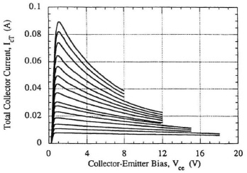
FIGURE 7.39 I–V characteristics for BB HBTs (after Liu et al., Ref. 35 © IEEE).
Figure 7.41 shows the large-signal output versus the input power for EB and BB HBTs measured at 9 GHz. Each HBT has an eight-finger unit cell, with a total emitter area of 800 μm2. The two transistors are physically adjacent, making comparison meaningful. The UB HBTs are found to operate improperly under these operating conditions, possibly due to thermal instability occurring in part of the RF cycle. Therefore, only the results of the BB HBT and the EB HBT are compared. The collector bias was between 9 and 10 V to maximize the output power. It is clear from Fig. 7.41 that the BB HBT consistently has larger output power and power-added efficiency across the input power range. Figure 7.42 shows the frequency dependence of the large-signal performance. Each data point represents the average result of five devices. The input RF power is fixed at 24 dBm. As shown in Fig. 7.42, the collector efficiency of the BB HBT maintains at about 70% throughout the measured band between 8.5 and 10.5 GHz, whereas it decreases to about 55% for the EB HBT as frequency increases. The significant difference in the collector efficiency is attributed to the difference in the power dissipations across the ballasted resistors. Because the bypass capacitance effectively shunts the RF signal away from the ballasted resistor in the BB HBT, all of the RF signal goes through the ballasted resistor in the EB HBT. The large signal power is larger in the BB HBT by about 0.5 dB. This leads to the larger output power consistently measured from the BB HBT. The combined superiority in both the collector efficiency and the output power naturally results in the larger power added efficiency observed in the BB HBT. These results demonstrate that base ballasting is the preferred ballasting scheme, not only because it guarantees absolute thermal stability at de, but also results in better large-signal performance at RF.
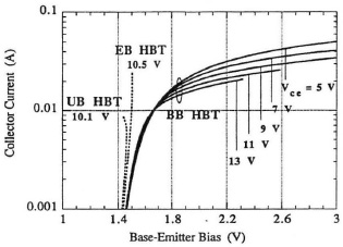
FIGURE 7.40 Regression characteristics of UB, EB, and BB HBTs (after Liu et al., Ref. 35 © IEEE).

FIGURE 7.41 Output power versus input power (after Liu et al., Ref. 35 ©IEEE).

FIGURE 7.42 Output power, collector efficiency, and power-added efficiency versus frequency (after Liu et al., Ref. 35 © IEEE).
REFERENCES
1. S. Tiwari, Compound Semiconductor Device Physics, Academic Press, San Diego, CA (1992).
2. S. M. Sze, Physics of Semiconductor Devices, 2nd ed., Wiley, New York (1981).
3. J. J. Liou and J. S. Yuan, “Modeling the reverse base current phenomenon due to avalanche effect in advanced bipolar transistors,” IEEE Trans. Electron Devices, ED-37, 2274 (1990).
4. E. Zanoni, E. F. Crabbè, J. M. C. Stork, P. Pavan, G. Verzellesi, L. Vendrame, and C. Canali, “Measurements and simulation of avalanche breakdown in advanced Si bipolar transistors,” International Electron Device Meeting, 927 (1992).
5. T. M. Liu, T.-Z. Chiu, V. D. Archer, and H. H. Kim, “Characteristics of impact-ionization current in the advanced self-aligned polysilicon-emitter bipolar transistor,” IEEE Trans. Electron Devices, ED-38, 1845 (1991).
6. K. Sakui, T. Hasegawa, T. Fuse, S. Watanabe, K. Ohuchi, and F. Masuoka, “A new static memory cell based on the reverse base current effect of bipolar transistors,” IEEE Trans. Electron Devices, ED-36, 1215 (1989).
7. P.-T. Lu and T.-C Chen, “Collector–base junction avalanche effects in advanced double-poly self-aligned bipolar transistors,” IEEE Trans. Electron Devices, ED-36, 1182 (1989).
8. E. Zanoni, R. Malik, P. Pavan, J. Nagle, A. Paccagnella, and C. Canali, “Negative base current and impact ionization phenomenon in AlGaAs/GaAs HBTs,” IEEE Electron Device Lett., EDL-13, 253 (1992).
9. T. K. Liu, T.-Y. Chiu, C. D. Archer III, and H. H. Kim, “Characteristics of impact-ionization current in the advanced self-aligned polysilicon-emitter bipolar transistor,” IEEE Trans. Electron Devices, ED-38, 1845 (1991).
10. E. Zanoni and G. Zandler, “Experimental and Monte Carlo analysis of impact-ionization in AlGaAs/GaAs HBTs,” IEEE Trans. Electron Devices, ED-43, 1769 (1996).
11. C. Canali, P. Pavan, A. D. Carlo, P. Lugli, R. Malik, M . Manfredi, A. Neviani, and L. Vendrame, “Dead-space effects under near-breakdown conditions in AlGaAs/GaAs HBTs,” IEEE Electron Device Lett., EDL-14, 103 (1993).
12. E. Zanoni, E. F. Crabbè, J. M. C. Stork, P. Pavan, G. Verzellesi, L. Vendrame, and C. Canali, “Extension of impact-ionization multiplication coefficient measurements to high electric fields in advanced Si BJTs,” IEEE Electron Device Lett., EDL-14, 69 (1993).
13. G.-B. Hong and J. G. Fossum, “Implementation of nonlocal model for impact ionization cunrrenl in bipolar circuit simulation and application to SiGe HBT design optimization,” IEEE Trans. Electron Devices, ED-42, 166 (1995),
14. Y. Apanovich, P. Blakey, R. Cottle, E. Lyumkis, B. Polsky, A. Shur, and A. Tcherniaev, “Numerical simulation of submicrometer devices including coupled nonlocal transport and nonisothermal effects,” IEEE Trans. Electron Devices, ED-42, 890 (1995).
15. B. Jalali, Y.-K. Chen, R.N. Nottenburg, D. Sivco, D. A. Humpherey, and A. Y. Cho, “Influence of base thickness on collector breakdown in abrupt AllnAs/InGaAs heterojunction bipolar transistors,” IEEE Electron Device Lett., EDL-11, 400 (1990).
16. C. L. Anderson and C. R. Crowell, “Threshold energies for electron–hole pair production by impact ionization in semiconductors,” Phys. Rev. B, 5, 2267 (1972).
17. J. S. Yuan and J. Ning, “Effect of impact ionization on Cjc of heterojunction bipolar transistors,” Solid-State Electron., 3, 742 (1995).
18. R. J. Malik, N. Chand, J. Nagle, R. W. Ryan, K. Alavi, and A. Y. Cho, “Temperature dependence of common-emitter I–V collector breakdown voltage characteristics in AlGaAs/GaAs and AllnAs/GalnAs HBTs grown by MBE,” IEEE Electron Device Lett., EDL-13, 557 (1992).
19. B. Jalali and S. J. Pearton, eds., InP HBTs: Growth, Processing, and Applications, Artech House, Norwood, MA (1995).
20. H. F. Chau, J. Hu, D. Pavlidis, and K. Tomizawa, “Breakdown-speed considerations in AlGaAs/GaAs heterojunction bipolar transistors with special collector design,” IEEE Trans. Electron Devices, ED-39, 2711 (1992).
21. H.-F. Chau, D. Pavlidis, J. Hu, and K. Tomizawa, “Breakdown-speed considerations in InP/InGaAs single-and double-heterostructure bipolar transistors,” IEEE Trans. Electron Devices, ED-40, 2 (1993).
22. X. Gui, G.-B. Gao, and H. Morkoç, “Simulation study of peak junction temperature and power limitation of AlGaAs/GaAs HBTs under pulse and CW operation,” IEEE Electron Device Lett., EDL-13, 411 (1992).
23. W. Liu, S. Nelson, D. Hill, and A. Khatibzadeh, “Current gain collapse in microwave multifinger heterojunction bipolar transistors operated at very high power density,” IEEE Trans. Electron Devices, ED-40, 1917 (1993).
24. L. L. Liou and B. Bayraktaroglu, “Thermal stability analysis of AlGaAs/GaAs hetero-junction bipolar transistors with multiple emitter fingers,” IEEE Trans. Electron Devices, ED-41, 629 (1994).
25. W. Liu, “The interdependence between the collapse phenomenon and the avalanche breakdown in AlGaAs/GaAs power heterojunction bipolar transistors,” IEEE Trans. Electron Devices, ED-42, 591 (1995).
26. W. Liu, H.-F. Chau, and E. Beam III, “Thermal properties and thermal instabilities of InP-based heterojunction bipolar transi stors,” IEEE Trans. Electron Devices, ED-43, 388 (1996).
27. W. Liu and A. Khatibzadeh, “The collapse of current gain in multi-finger heterojunction bipolar transistors: its substrate temperature dependence, instability criteria, and modeling,” IEEE Trans. Electron Devices, ED-41, 1698 (1994).
28. I. E. Getreu, Modeling the Bipolar Transistor, Elsevier, New York (1978).
29. P. L. Hower and P. K. Govil, “Comparison of one- and two-dimensional models or transistor thermal instability,” IEEE Trans. Electron Devices, ED-40, 1917 (1993).
30. G.-B. Gao, M. S. Unlu, H. Morkoy, and D. Blackburn, “Emitter ballasting resistor design for, and current handling capability of AlGaAs/GaAs power heterojunction bipolar transistors,” IEEE Trans. Electron Devices, ED-38, 185 (1991).
31. B. Bayraktaroglu, J. Barrette, L. Kehias, C. I Hunag, R. Fitch, R. Neikhard, and R. Scherer, “Very high-power-density CW operation of GaAs/AlGaAs microwave heterojunction bipolar transistors,” IEEE Electron Device Lett., EDL-40, 493 (1993).
32. J. Sewell, L. L. Liou, D. Barlage, J. Barrette, C. Bozada, R. Dettmer, R. Fitch, T. Jenkins, R. Lee, M. Mack, G. Trombley, and P. Watson, “Thermal characterization of thermallyshunted heterojunction bipolar transistors,” IEEE Trans. Electron Devices, ED-17, 19 (1996).
33. M.G. Adlerstein and M.P. Zaitlin, “Thermal resistance measurements for AlGaAs/GaAs heterojunction bipolar transistors,” IEEE Trans. Electron Devices, ED-38, 1553 (1991).
34. J. R. Waldrop, K. C. Wang, and P.M. Asbeck, “Determination of junction temperature in AlGaAs/GaAs heterojunction bipolar transistors by electrical measurement,” IEEE Trans. Electron Devices, ED-39, 1248 (1992).
35. W. Liu, A. Khatibzadeh, J. Sweder, and H.-F. Chau, “The use of base ballasting to prevent the collapse of current gain in AlGaAs/GaAs heterojunction bipolar transistors,” IEEE Trans. Electron Devices, ED-43, 245 (1996).
PROBLEMS
7.1. Show that when the avalanche process is initiated by electrons, the avalanche integral of interest is related by the equation
![]()
7.2. Derive the multiplication factor as a function of αn and E(x).
7.3. Compare the collector–base junction capacitance with and without avalanche effect for local and nonlocal models.
7.4. Derive the Early voltage, including avalanche effect.
7.5. Derive the free carrier capacitance using the expression
![]()
where Δp = p(O)(M − 1) and M = 1/[1 − (V / BVCB0)n].
7.6. A two-finger HBT has an area of 2 × 20 μm2 of each finger sitting on top of a 100-μm GaAs substrate. Assume that the mutual thermal coupling between theμ two fingers is negligible. Estimate the thermal resistance of each of the fingers . What is the overall thermal resistance of the two-finger device?
7.7. Explain qualitatively the thermal stability of multifinger Si BJTs and SiGe HBTs.
7.8. Discuss how to design the HBT to improve thermal stability.