
CHAPTER EIGHT
Reliability
Heterojunction bipolar transistors have demonstrated excellent performance for high-frequency IC applications and for insertion of this technology into practical systems. The ultimate usefulness of this technology for system applications is determined by its reliability. The reliability-related parameters of interest, such as failure rates, mean time to failure (MTTF), and activation energies, are commonly determined by stressing devices and circuits under high forward biases and/or elevated temperatures. This procedure is known as high-current and high-temperature accelerated aging or life testing. The interpretation of the statistical life-test data is very important to ensure that the high-temperature and high-current stress tests induce realistic failures, which are expected under normal operating conditions. For bipolar transistors it is important to determine the actual device junction temperature or “hot spot” under biased-stress conditions. The junction temperature differential depends on the device thermal resistance, device size, and temperature.
8.1 ELECTRICAL AND THERMAL OVERSTRESS
Reliability requirements are dictated by the application. Reliability qualification work is aimed at establishing robust process and design rules for achieving high mean time between failure. General HBT reliability testing includes stabilization bake, accelerated life testing, and step-stress testing. An initial stabilization bake is performed to stabilize the device parameters prior to accelerated aging and step-stress tests, and to screen for infant mortality. Devices are typically subject to 200 to 240°C for 48 hours in a nitrogen ambient atmosphere to stabilize dc parameters.
Accelerated life tests include aging at 200 to 260°C under dc bias with step-stress testing to extract the activation energy and MTTF for degradation designed to explore accelerated lifetimes. This is more realistic because high-temperature aging induces a failure mechanism that may never be encountered in normal operation conditions. High-temperature testing is performed to reduce the time needed to achieve median lifetimes.
Reliability testing of GaAs HBTs has focused on accelerated aging of discrete devices under normal operating dc bias. The packaged devices are removed periodically and tested for dc current gain, base–emitter turn-on voltage, ohmic contact resistance, and junction leakage. Figures 8.1a–d show the experimental data of base–emitter leakage current, current gain, collector–emitter offset voltage, and base–collector leakage versus stress time. These key parameters enable test engineers to assess the stability and integrity of the base–emitter junction, the base layer, and the base–collector junction [1,2]. The base–emitter leakage current in Fig. 8.1a is seen to decrease steadily and uniformly with increasing stress time in the test population. The current gain in Fig. 8.1b has an initial increase of approximately 10%, which is attributed to a reduction in the surface recombination velocity as a result of exposure to high temperature. As the stress increases, this process reverses and the current gain decays gradually. The offset voltage increases with stress time as shown in Fig. 8.1c. Intially, the offset voltage is unchanged. It is then followed by a period of stress time and displays an identical trend to that of the base–collector leakage increase in Fig. 8.1d. It is clear that the leakage current decreases steadily in approximately the first 300 hours of stress. This is then followed by a rapid increase in the leakage current of the base–collector junction. The increase in the leakage current occurs very uniformly over a short interval of time, as opposed to the case where the degradation spreads out over the entire length of the stress period. This feature is highly desirable. The confinement and the uniformity of device degradation results in a failure distribution for the life-test population, which has a very low dispersion. Another apparent feature is the lack of early device failures or rapid degradation in the early hours of stress, known as infant mortality.
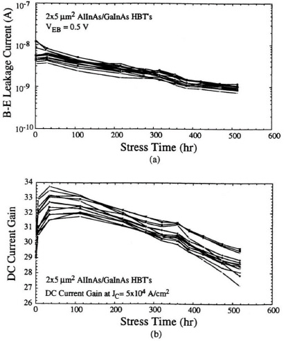

FIGURE 8.1 (a) Base–emitter leakage current and (b) current gain versus stress time (after Hafizi et al., Ref. 1 © IEEE). (c) Collector–emitter offset voltage and (d) base–collector leakage current versus stress time (after Hafizi et al., Ref. 1 © IEEE).
8.1.1 Forward- and Reverse-Bias Stress Effects
When bipolar transistors are forward-biased at high current densities, changes in the transistor performance characteristics, including leakage currents, parasitic resistances, and current gain can result. As bipolar technology is scaled to smaller dimensions, the operating current densities increase and the implications of forward-bias degradation for device design are of increasing concern.
Studies by Hemmert et al. [3,4] showed that forward bias stress induced gradual current gain degradation due to an increase in base current. They attributed the gain changes to electromigration. Other physical mechanisms to explain the gain degradation, such as Auger recombination, produced hot electrons were reported [5]. Sun et al. [6] examined forward-biased stress effects on silicon bipolar transistors in gain and noise characteristics. Test bipolar transistors from three different fabrication technologies were used. Type A devices were fabricated by conventional oxide isolation techniques with emitter dimensions of 2.5 μm × 4.3 μm. Type B devices were fabricated with polysilicon base contacts and sidewall oxide, which had emitter dimensions of 1.5 μm × 2.0 μm. Metal contacts were via metal studs through oxide vias to reduce eletromigration-induced stress directly over the transistor contacts. Type C devices are from a test structure [2] designed particularly to investigate electromigration effects. Type C devices have emitter dimensions of 2.5 μm × 4.0 μm. Transistors were stressed with the base–collector junction short-circuited and the base–emitter junction forward biased. There was no reverse-biased junction to eliminate the possibility of degradation due to reverse-bias produced hot electrons. The temperature of the stressed devices was varied between −75 and 240°C. Stressing was interrupted at selected times to measure the Gummel plots and the noise spectra of the stressed devices. Control devices were used that received temperature stress but not electrical stress. Device measurements were performed at a temperature of 23 ± 1°C in an environmental chamber.
Stress effects on bipolar current gain have been studied. Figure 8.2 shows current gain versus base–emitter bias for technology A transistor. The forward stressing was done at 240°C with a current density of 2 mA/μm2. These devices showed a pronounced and systematic gradual degradation of current gain with increasing stress time when subject to a combination of high forward-bias current and temperature. Normalized current gain (average current gain after stress/average current gain before stress) versus stress time at different current levels and ambient temperatures is shown in Fig. 8.3. In this plot solid squares represent 1 mA/μm2 at −75°C, empty squares 1 mA/μm2 at l75°C, solid circles 1 mA/μm2 at 240°C, and triangles 2 mA/μm2 at 240°C. The resulting gain degradation after 500-hour of stress at 240°C is approximately 20% when the stress current is 2 mA/μm2 and approximately 10% after 750 hours when the stress current is 1 mA/μm2. No degradation was observed during the 500-hour stress with ambient temperatures of −75 and 175°C. The gradual degradation and the temperature dependence is consistent both with electromigration-induced compressive stress and with Auger hot-electron-induced damage.
For type B devices, the degradation was quite different than for type A devices. Figure 8.4 shows the result of forward-bias stress with 5 mA/μm2 at a temperature of 225°C. No systematic change was observed up to 100 hours, but significant degradation occurs later. In contrast to the result for type A technology, degradation for a given device was precipitous rather than gradual. Once degradation had begun, in about 30 to 40 hours the process culminated in an open-circuit transistor. The time required for 50% drop out of the population was approximately 400 hours. The nature of the failure is indicative of electromigration. Electromigration opens in the line initially, which produces an increase in series resistance and results in an open circuit when a line is opened completely. Scanning electron microscopy (SEM) confirmed this conclusion.

FIGURE 8.2 Current gain versus base–emitter voltage (after Sun et al., Ref. 6 © IEEE).

FIGURE 8.3 Normalized current gain versus stress time for technology A device (after Sun et al., Ref. 6 © IEEE).

FIGURE 8.4 Current gain versus stress time for technology B device (after Sun et al., Ref. 6 © IEEE).
The gain degradation on type C devices is displayed in Fig. 8.5. The transistor that received the direct electrical stress shows the largest degradation in current gain after 500 hours of stressing with 5 mA/μm2 at 200°C. For the other transistors, the gain degradation decreases with increasing distance from the first transistor, consistent with expectations for electromigration-induced compressive stress. For all type C transistors, the decrease in gain is due to an increase in base current.
The low-frequency noise characteristics were also measured for the three different bipolar technologies. In each case the noise measurement was done with a base–emitter bias in the range 0.77 to 0.82 V, corresponding to emitter currents below 0.5 mA. Under these bias conditions, the shot noise is much less than the 1/f noise in the frequency range 1 to 100 Hz. The technology C transistors were stressed with a current density of 5 mA/μm2 at T = 200°C for up to 500 hours. As shown in Fig. 8.6, the noise initially dropped for measurements taken after 1 hour of stress. Subsequent noise measurement of cumulative stress showed an increase in noise level with stress time. This noise decrease is in contrast to noise changes caused by hot-electron-induced stress since hot electrons produce an increase in noise [7]. Experiments performed on both technology A and B transistors show similar noise characteristic changes due to forward-bias stress. Technology A transistors showed an initial decrease in low-frequency noise when stressed at 240°C with a current density of 2 mA/μm2. After a noise minimum is reached, the noise for technology A devices eventually increases with longer stress time (i.e., 100 hours of cumulative stress). This behavior is similar to that observed for technology C transistors. For both technology A and C transistors, the noise starts to increase, after its initial decrease, at about the same time that the gain begins to drop substantially. Technology B transistors also show a drop in the low-frequency noise characteristics as shown in Fig. 8.7. This technology, however, did not show the later increase in the low-frequency noise as did the other technologies. Note that technology B transistors did not show a gradual gain degradation as did technology A and C devices; rather, they showed an abrupt failure due to open circuits caused by electromigration.
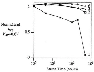
FIGURE 8.5 Normalized current gain versus stress time for technology C device (after Sun et al., Ref. 6 © IEEE).
Comparison of time to failure of SiGe and Si bipolar transistors has been made [8]. The effects of Ge in the epitaxial base on the reliability of SiGe HBTs were investigated. The 10-year time to failure under emitter–base junction reverse-bias stress was measured at the designed operation voltage by the current-acceleration method and compared to that of Si BJTs with no Ge content in the base. High-performance Si and SiGe bipolar transistors were fabricated epitaxially on Si wafers using rapid thermal chemical vapor deposition (RTCVD) technology [9]. Substrates were ![]() 100
100![]() Si:Sb (2 × 10¹⁸ Sb/cm−3). Following growth of 2.5-μm Si collector (5 × 10¹⁵ As/cm3), the active regions were isolated by a modified LOCOS process and RCA-cleaned prior to nonselective deposition of the SiGe base. Boron implantation in the extrinsic base was then performed, and an oxide/nitride stack was deposited and etched to open the emitter region followed by a polysilicon and As implant. All implants were activated by a single RTA. A 3000-Å undoped low-T oxide was then deposited. Contacts were then opened followed by TiW/AlCuSi metallization. The Ge concentration in the base and the dopant impurity concentrations were measured by SIMS. The Ge content is linearly graded from 0% at the emitter–base junction to a peak of 10% at the base–collector junction. The base dopant density is nearly constant (ca. 4 × 1018 cm−3), and the base thickness is about 800 Å. The baseline Si BJT was fabricated with identical fabrication steps except that it has no Ge in the quasi-neutral base. The TEM cross section does not show dislocations in the SiGe base indicating that the SiGe layer is not relaxed after the fabrication is completed.
Si:Sb (2 × 10¹⁸ Sb/cm−3). Following growth of 2.5-μm Si collector (5 × 10¹⁵ As/cm3), the active regions were isolated by a modified LOCOS process and RCA-cleaned prior to nonselective deposition of the SiGe base. Boron implantation in the extrinsic base was then performed, and an oxide/nitride stack was deposited and etched to open the emitter region followed by a polysilicon and As implant. All implants were activated by a single RTA. A 3000-Å undoped low-T oxide was then deposited. Contacts were then opened followed by TiW/AlCuSi metallization. The Ge concentration in the base and the dopant impurity concentrations were measured by SIMS. The Ge content is linearly graded from 0% at the emitter–base junction to a peak of 10% at the base–collector junction. The base dopant density is nearly constant (ca. 4 × 1018 cm−3), and the base thickness is about 800 Å. The baseline Si BJT was fabricated with identical fabrication steps except that it has no Ge in the quasi-neutral base. The TEM cross section does not show dislocations in the SiGe base indicating that the SiGe layer is not relaxed after the fabrication is completed.
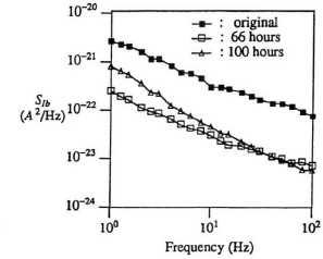
FIGURE 8.6 Noise versus frequency for technology A device (after Sun et al., Ref. 6 © IEEE).

FIGURE 8.7 Noise versus frequency for technology B device (after Sun et al., Ref. 6 © IEEE).
Figure 8.8 shows the time to failure (TTF) versus reverse emitter–base stress voltage of the SiGe and Si bipolar transistors. The TTF was obtained from two stress and measure experiments: (1) the open-collector (OC) method, and (2) the forward-collector (FC) method, using VBC in the range 0.75 to 0.9 V. First, the integrated terminal charge to failure, QTF = QEB-stress = ≡ ∫ jE-stress (t) dt required for ΔβF = −10% at VBE = 0.76 V, is plotted against the stress voltage VBE-stress for both OC and FC measurements. Then the FC data are normalized twice with respect to the OC data to account for the different geometrical current distributions and the kinetic energy difference between the bond-breaking hot carriers at the two bias conditions. The TTF is then obtained by dividing the normalized QTF data by the open-collector emitter current JE-stress. It is clear from Fig. 8.8 that the TTF is not affected by Ge. The slightly higher TTF in the SiGe HBTs may be due to a smaller reverse current. Note that the OC data (open circles and triangles) gave TTF only for VEB-stress > 2.75 V because of the long stress time (> 105 s) required at lower stress voltages. This OC TTF increases rapidly beyond reasonable time as the stress voltage is lowered below 2.75 V. The current-accelerated FC data (filled circles and triangles), however, gave TTF as high as 2.3 × 10⁹ s (ca. 745 years). From Fig. 8.8 the 10-year TTF was attained when VEB-stress ≤ 2.2 V in the Si BJT and VEB-stress ≤ 2.26 V in the SiGe HBT.

FIGURE 8.8 TTF as a function of VEB-stress (after Neugroschel et al., Ref. 8 © IEEE).
8.1.2 Thermal Overstress
The thermal stress test is performed at given bias conditions and at elevated ambient temperatures, assuming that the failure mechanisms are thermally accelerated. Discrete devices with a substrate thickness of 100 μm were packaged to perform the accelerated life test [1]. The transistors were biased in the forward active mode with a constant collector current density of 7 × 10⁴ A/cm. Over 2,500 hours of accelerated life test was carried out at 193, 208, and 228°C ambient temperatures. Extensive dc characterization was performed periodically during the life test. For devices with compositionally graded base–emitter junctions, an increase of approximately 1.8 m V in VBE per angstrom of Be diffusion was determined. This indicates that the VBE is a very sensitive parameter for monitoring the stability of the Be. Collector–emitter offset voltage and junction leakage currents were also recorded to monitor the stability of the base–emitter and base–collector junctions.
Figure 8.9 shows measured base–emitter and base–collector junction leakage currents before and after stress at 208°C. At low base–emitter biases, the base current decreases and leads to an increase of about 10% in the dc current gain. The base–emitter junction leakage currents, in both forward and reverse biases, decreased steadily under stress. The crystallographic orientation of the emitter mesa or a Si3N4 surface passivation did not have any effect on the stability of the B-E junction, due to the use of a nine-period superlattice inserted between the Be-doped GaInAs base and the AlInAs emitter. The superlattice effectively blocks the movement of any interstitial Be+ diffusion from the base into the emitter. The base–collector leakage current in the reverse bias (see Fig. 8.9b) increases rapidly as the bias stress progresses. In the forward bias region, in addition to an emerging leakage current, the turn-on voltage of the junction also steadily decreases. The stress-increased leakage current has a voltage dependence of exp(q VBE/nkT), where n increases from 1 to greater than 2 as the stress progresses. When the junction is under reverse bias, surface states are generated by hot electrons at or near the metallurgical junction where the electric field is greatest. The interface traps act as generation–recombination centers, causing an increase in the reverse leakage current and the nonideal current in the forward direction. The stress-induced leakage currents of the B-C junction correlate with the amount of reverse-bias voltage applied to the B-C junction.

FIGURE 8.9 (a) Base emitter and (b) base–collector currents before and after stress at 208°C (after Jalali and Pearton, Ref. 10 © Artech House).
Reliability of InP-based HBTs has been demonstrated for applications requiring MTTF in excess of 107 hours (at l25°C junction temperature) at high current drive levels. It appears that because of the excellent reliability performance, low-power operation, and relative ease of fabrication for this new technology, there are excellent prospects for insertion of InP-based integrated circuits into practical products in commercial and space applications. Figure 8.10 shows a failure plot for an InP-based HBT biased at VCE = 2 and 3 V. In this plot the logarithm of time to failure is shown as a function of cumulative failure distribution. The 50% cumulative failure point in this graph yields the MTTF value for each of the life tests. The MTTF values obtained were 22, 122, and 390 hours at different IC, VCE, and temperatures. The dispersion (σ) of the log-normal distribution is approximately 0.3. The σ is estimated as log(time to 50% failure) minus log(time to 16% failure). There is no apparent change in the value of σ over the range of temperature of the tests, indicating the validity of the accelerated stress experiments. From an Arrhenius plot of the MTTF values (figure not shown here), an activation energy of 1.92 eV was obtained and a MTTF of 1.23 × 10⁷ hours at 125°C junction temperature was projected. The MTTF at 50°C junction temperature is 5.7 × 10¹² hours. The low dispersion of the failure distribution observed in the life test data is desirable for system applications because it leads to a very small failure rate.

FIGURE 8.10 Failure plot for an HBT biased at VCE = 2 and 3 V (after Jalali and Pearton, Ref. 10 © Artech House).

FIGURE 8.11 Arrhenius plot for data shown in Fig. 8.10 (after Jalali and Pearton, Ref. 10 © Artech House).
Figure 8.11 shows an Arrhenius plot of MTTF for the 2 V and 3 V life tests. The projected MTTF is 2.16 × 10⁷ and 6.15 × 10⁶ hours, respectively, at a junction temperature of 125°C. For these predictions, the failure criterion was set as the collector–base leakage current ICB > 1% of IB at a reverse bias of VCE = 2.5 V. The activation energy was assumed to be 1.92 eV. A similar reliability performance has been predicted for double-heterojunction bipolar transistors incorporating an InP collector [11]. The failure mechanism and the performance degradation in InP-based DHBTs is identical to that of single-heterojunction devices.
8.1.3 Burn-in
Burn-in carried out in a high-temperature/current environment is used widely to assess the reliability of semiconductor devices. Such a test is particularly useful to determine the long-term performance of heterojunction bipolar transistors since semiconductor bulk and surface properties are susceptible to thermal and electrical stresses. Experimental results show that for a fixed bias condition, the burn-in could increase or decrease the base current of the HBT but does not change the collector current. An abnormal base current with an ideality factor of about 3 has been observed in the Gummel plot of an HBT [12] subject to a relatively long-hour burn-in test as shown in Fig. 8.12.
Two theories have been reported to explain the abnormal base current in the post-burn-in HBT [13, 14]. The first theory [13] suggests that defects in a semiconductor can redistribute themselves and diffuse to dislocations due to enhanced recombination process and/or high thermal energy. Since the HBT undergoing the burn-in test is subject to high temperature and high injection stresses, such a recombination/thermal-enhanced defect diffusion is a likely mechanism attributing to the unique post-burn-in behavior. The second theory [14] suggests that the abnormal current is attributed to a significant increase in the number of defects in the strained base. This is confirmed by deep-level transient spectroscopy, which indicates that the trapping states generated by the burn-in test are located in the base region.

FIGURE 8.12 Base and collector currents after burn-in (after Liou and Huang, Ref. 12 © Elsevier Science).
Note that burn-in could also result in a decrease of base current. This burn-in effect is suggested related to the interface between the passivation layer and the semiconductor in the extrinsic base surface region [15]. Correlation between the burn-in effect and the extrinsic base surface quality in carbon-doped GaInP/GaAs HBTs was studied [16]. The wafers employed for the fabrication of the HBTs were grown by MOCVD with different passivation techniques. Figure 8.13 shows cross sections of the investigated HBTs. Sample A devices have SiN passivation, while sample B devices have a ledge passivation. After an initial characterization, the devices were stressed at room temperature in the forward active region. During the stress the applied Collector–emitter voltage was 5.7 V and the stress collector current density was kept constant at 104 A/cm2. The base current variation of these two passivated devices versus stress time is shown in Fig. 8.14. A decrease of base current for both A and B samples has been observed. The SiN passivated devices exhibit a larger burn-in effect associated with a reduction of the base current. This burn-in effect is a surface-related phenomenon. The defects involved in the burn-in effect are probably located at the extrinsic base surface region and possibly at the passivation/semiconductor interface. From Fig. 8.14 it indicates that the ledge passivation may be a very promising technology to improve device stability and reliability.

FIGURE 8.13 Two device structures for the investigation of burn-in effect (after Borgarino et al., Ref. 16 © IEE).
8.2 PROCESS-RELATED RELIABILITY ISSUES
8.2.1 Base Dopant Out-diffusion
The effects of base dopant out-diffusion on SiGe [17] and GaAs [18] heterojunction bipolar transistors have been studied. Small amounts of base dopant out-diffusion from a heavily doped base into a more lightly doped emitter can seriously change the device performance, due to the formation of parasitic barriers. Once the barriers occur, the device performance cannot be recovered.
Consider an n-p-n SiGe heterojunction bipolar transistor with a flat Ge profile in the base. The interfaces between the Si–SiGe emitter–base junction and the SiGe–Si collector–base junction have abrupt dopant transitions. The entire base layer is heavily doped with boron in a boxlike profile. The transistor structures were grown in situ on a ![]() 100
100![]() n-type silicon substrate using RTCVD. After chemical cleaning, the wafers were loaded into the RTCVD reactor and baked in hydrogen carrier gas. Heavily doped n+ buffer layers and n-type collector layers doped about 5 × 1017 cm−3 were grown at 100°C. The p-type Si0.8Ge0.2 base has a doping of 1019 or 1020 cm−3 with 300-Å thickness and were grown at 850°C for 3 minutes. The base layers are strained because of a negligible number of misfit dislocations observed from TEM measurement. Base contact was established by boron implant, while emitter contact had a shallow arsenic implantation. The device was passivated with SiO2 film deposited by plasma deposition at 350°C. The implants were then annealed for 10 minutes at 800°C. Titanium–aluminum metallization and patterning were used at the end of processing.
n-type silicon substrate using RTCVD. After chemical cleaning, the wafers were loaded into the RTCVD reactor and baked in hydrogen carrier gas. Heavily doped n+ buffer layers and n-type collector layers doped about 5 × 1017 cm−3 were grown at 100°C. The p-type Si0.8Ge0.2 base has a doping of 1019 or 1020 cm−3 with 300-Å thickness and were grown at 850°C for 3 minutes. The base layers are strained because of a negligible number of misfit dislocations observed from TEM measurement. Base contact was established by boron implant, while emitter contact had a shallow arsenic implantation. The device was passivated with SiO2 film deposited by plasma deposition at 350°C. The implants were then annealed for 10 minutes at 800°C. Titanium–aluminum metallization and patterning were used at the end of processing.
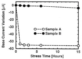
FIGURE 8.14 Base current variation versus stress time at VCE = 1.4 V and IC = 4 mA (after Borgarino et al., Ref. 16 © IEE).
The valence-band discontinuity ΔEv for a strained Si1−xGx layer grown on ![]() 100
100![]() Si is close to the total bandgap difference between Si and SiGe [19]. Autodoping at interfaces during growth or boron out-diffusion into the adjacent silicon layers during growth can move the electrical p-n junction into the silicon emitter and collector regions [20]. Figure 8.15 shows that even small amounts of boron out-diffusion cause large parasitic barriers for electrons at both emitter–base and collector–base heterojunctions when the device is in forward-active mode. For example, for an out-diffusion length of 25 Å, a parasitic barrier of a height of 80 meV is formed at the emitter–base junction. This parasitic barrier impedes electrons injected from emitter to base and degrades the emitter efficiency and collector current. The overall barrier for holes traveling from base to emitter, however, is not changed. Device simulation results of normalized collector current versus inverse temperature for different out-diffusion lengths are shown in Fig. 8.16. In Fig. 8.16 curves (a), (b), (c), and (d) correspond to no out-diffusion and LD = 25, 50, and 75 Å, respectively. Curve (e) corresponds to LD = 25 Å with 100 Å spacer. The devices with out-diffusion have significant collector current degradation. The out-diffusion also reduces the slope of the collector current versus inverse temperature. The degradation in heavily doped devices indicates that the parasitic barrier effect is much larger than any beneficial effect of bandgap narrowing in the heavily doped bases. In addition, severe degradation is expected for more heavily doped bases because of the higher doping levels in the out-diffusion tails and because of the linear dependence of the boron diffusion coefficient on boron concentration [20].
Si is close to the total bandgap difference between Si and SiGe [19]. Autodoping at interfaces during growth or boron out-diffusion into the adjacent silicon layers during growth can move the electrical p-n junction into the silicon emitter and collector regions [20]. Figure 8.15 shows that even small amounts of boron out-diffusion cause large parasitic barriers for electrons at both emitter–base and collector–base heterojunctions when the device is in forward-active mode. For example, for an out-diffusion length of 25 Å, a parasitic barrier of a height of 80 meV is formed at the emitter–base junction. This parasitic barrier impedes electrons injected from emitter to base and degrades the emitter efficiency and collector current. The overall barrier for holes traveling from base to emitter, however, is not changed. Device simulation results of normalized collector current versus inverse temperature for different out-diffusion lengths are shown in Fig. 8.16. In Fig. 8.16 curves (a), (b), (c), and (d) correspond to no out-diffusion and LD = 25, 50, and 75 Å, respectively. Curve (e) corresponds to LD = 25 Å with 100 Å spacer. The devices with out-diffusion have significant collector current degradation. The out-diffusion also reduces the slope of the collector current versus inverse temperature. The degradation in heavily doped devices indicates that the parasitic barrier effect is much larger than any beneficial effect of bandgap narrowing in the heavily doped bases. In addition, severe degradation is expected for more heavily doped bases because of the higher doping levels in the out-diffusion tails and because of the linear dependence of the boron diffusion coefficient on boron concentration [20].

FIGURE 8.15 Out-diffused doping profile characteristics (after Prinz et al., Ref. 17 © IEEE).
The reliability characteristics of AlGaAs/GaAs n-p-n bipolar transistors with beryllium and carbon-doped base layers have been investigated [18]. Reliability assessment was based on a constant-stress life test conducted at three temperatures and using the dc current gain as the critical device parameter. For this life test, a 10% degradation in prestress current gain at a 1-mA collector current was established as the failure criteria. The experiment is a constant-stress lifetime at 240, 260, and 280°C ambient temperature. Over 215 discrete HBTs were studied. Postepitaxial growth processing is assumed to be identical over the various wafers. Electrical testing at 25°C was done periodically to monitor degradation in dc current gain at 1-mA. The life test with periodic electrical testing was continued until greater than 70% of a cell’s population failed. During thermal stress, all HBTs, excluding control devices, were subject to a forward bias of VCE = 3 V and IC = 2 mA (6.67 × 10³ A/cm). No RF bias was applied during thermal stress.

FIGURE 8.16 Normalized collector current versus inverse temperature (after Prinz et al., Ref. 17 © IEEE).

FIGURE 8.17 Failure time versus cumulative failure of Be-doped devices (after Yamada et al., Ref. 18 © IEEE).
Figure 8.17 shows the cumulative failure of the Be device EM+ at 570°C. For this group of devices, the standard deviation σ = 0.7 was calculated by least-squares fitting of the log-normal distribution. The failure time decreases with increasing temperature, as expected. An Arrhenius plot illustrating median life versus inverse junction temperature is shown in Fig. 8.18. Compensation for an estimated junction temperature rise of 12°C over ambient temperature has been accounted for in Fig. 8.18. The calculated activation energy for Be/570, Be/570, EM+, Be/580, and carbon devices are 1.52, 1.77, 1.19, and 0.86 eV, respectively. The difference between the Be/570 and the Be/570,EM+ device in fabrication is that in the latter device the subsequent emitter layer growth was performed at an elevated substrate temperature. At 125°C the MTTF is 8.4 × 10⁷, 1.87 × 10⁸, 3.3 × 10⁶, and 4.2 × 10⁵ hours for Be/570, Be/570, EM+, Be/580, and carbon devices, respectively.

FIGURE 8.18 MTTF current versus inverse temperature (after Yamada et al., Ref. 18 © IEEE).
For the Be-doped HBTs, the dominant failure mechanism is the diffusion of interstitial beryllium (Be+) from the base to graded base–emitter AlGaAs during forward bias operation. In devices with compositional grading at the base–emitter junction, the steady diffusion of the Be+ displays the p-n junction by moving it gradually into the graded region (toward the emitter) as the bias stress progresses. As a result of Be+ redistribution, a potential spike in the conduction-band at the emitter–base junction is formed. This increases the device turn-on voltage and causes a severe decrease in the dc current gain. The diffusion of interstitial Be+ from the base into the emitter is activated only under applied bias and is accelerated by temperature. This mechanism differs from growth-related Be diffusion [21], which is thermally activated. The bias-dependent Be diffusion widely reported for AlGaAs/GaAs HBTs depends strongly on the Be doping level and the amount of bias applied during the stress. It is also affected by the crystallographic orientation of the emitter mesa, such as [011], [010], or [0![]() 1] and by surface passivation films on the base–emitter junction. Low substrate growth temperature and a high As/Ga flux ratio during MBE growth of beryllium could suppress Be+ formation, resulting in reliable Be-doped HBTs. Lower Be-doping concentration improves device reliability also [22]. The failure mechanism is believed to be the same for all three Be groups. For carbon-doped HBTs the median lifetime is highest among all four groups at 260 and 280°C and second highest at 240°C. However, its low activation energy projects a MTTF at 125°C that is lowest among the four HBT groups in Fig. 8.18. In GaAs, the carbon has a high acceptor efficiency, and low diffusivity. This value of the diffusion coefficient is at least three orders of magnitude smaller than the value for beryllium. Thus a carbon-doped base improves the device reliability.
1] and by surface passivation films on the base–emitter junction. Low substrate growth temperature and a high As/Ga flux ratio during MBE growth of beryllium could suppress Be+ formation, resulting in reliable Be-doped HBTs. Lower Be-doping concentration improves device reliability also [22]. The failure mechanism is believed to be the same for all three Be groups. For carbon-doped HBTs the median lifetime is highest among all four groups at 260 and 280°C and second highest at 240°C. However, its low activation energy projects a MTTF at 125°C that is lowest among the four HBT groups in Fig. 8.18. In GaAs, the carbon has a high acceptor efficiency, and low diffusivity. This value of the diffusion coefficient is at least three orders of magnitude smaller than the value for beryllium. Thus a carbon-doped base improves the device reliability.
8.2.2 Sensitivity of Emitter–Base Junction Design
Base out-diffusion changes not only the collector current but also the ideality factor, Early voltage, and device switching speed. The simulations and experiments in [23] show that a strong correlation exists between the drop of collector saturation current, an increase of its ideality factor, and a rise in the switching time due to additional emitter delay from the parasitic barrier effects [24].
Examining Eq. (5.10), it is clear that the small part of the base dopant that lies outside the SiGe layer affects the integral significantly, due to the smaller ![]() in silicon. Although a very small fraction of the total base dopant is involved, the change in collector saturation current density may be significant. By the same token, a modulation of the space charge layer will cause an enormous variation in the effective base Gummel number, resulting in a low Early voltage or an ideality factor greater than 1, depending on whether the side of the out-diffusion is at the base–collector or base–emitter junction.
in silicon. Although a very small fraction of the total base dopant is involved, the change in collector saturation current density may be significant. By the same token, a modulation of the space charge layer will cause an enormous variation in the effective base Gummel number, resulting in a low Early voltage or an ideality factor greater than 1, depending on whether the side of the out-diffusion is at the base–collector or base–emitter junction.
A SiGe HBT with base doping 5 × 1019 cm−3, emitter doping 1 × 1018 cm−3, and ideal abrupt doping profiles has been investigated using one-dimensional device simulation [23]. The valence-band discontinuity is about 200 meV at 25% Ge content [25]. Its normalized collector current density, collector current ideality factor, and emitter–base delay time as a function of the Si/SiGe interface position with respect to the p-n junction at x = 0 are shown in Fig. 8.19. Consider the ideal abrupt doping profile, which is represented by the curve a in Fig. 8.19. At x = 0 the Si/SiGe interface and the p-n junction coincide. The Si/SiGe interface lies within the base for x > 0 and within the emitter for x < 0. In the case of x > 0, a rapid decrease in collector saturation current density can be observed with increasing distance x because of the increase in the base Gummel number. At the same time the ideality factor rises due to formation of a parasitic conduction-band barrier. The ideality factor increases with interface position, reaches a maximum, and then drops when the barrier becomes too stable to be modulated by VBE. The emitter–base delay increases rapidly for x > 0. This is due to a reduction in electron injection into the emitter which increases the emitter delay. The emitter delay is important for an HBT with a heavily doped base and a lightly doped emitter. The base delay remains almost constant. Moving the Si/SiGe interface into the emitter (x < 0), the collector saturation current density, ideality factor, and emitter–base delay are essentially unchanged.
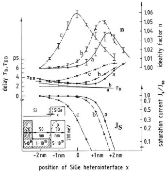
FIGURE 8.19 Jc, n, and E versus position (after Gruhle, Ref. 23 © IEEE).
When the rectangular base dopant profile has been broadened due to diffusion during growth, this leads to an error function distribution with NA/2 at the original step interface position. Curve b in Fig. 8.19 corresponds to a diffusion length of l = 2.5 nm, and a curve of c corresponds to l = 5 nm. The new position of the p-n junction moves 3.7 nm (curve b) and 7.4 nm (curve c) to the left. The general behavior of the SiGe HBT remains similar. At x > 0, parasitic barriers form when out-diffusion takes place, and both the ideality factor and emitter–base junction increase.
The out-diffusion effect may be improved by using an undoped spacer layer at the emitter–base heterojunction. Zhang et al. [26] performed short-term current stress tests on In0.53 Ga0.47As/In0.52Al0.48 As HBTs with lattice-matched and strained (tensile and compressive) spacer layers inserted between the base and emitter regions. No degradation of the dc and RF performance of the devices with a tensilely strained spacer layer was reported, while small changes in devices with lattice-matched and compressively strained spacer layers were recorded. The tensilely strained spacer layer is very effective in controlling the out-diffusion of Be dopant atoms from the base to the emitter region.
8.2.3 Influence of Dislocations on the Transistor Current Gain
The use of epitaxial layers grown on lattice-mismatched substrates can significantly expand the selection and combinations of material systems for various device applications. When the mismatched layer thickness becomes larger than the critical thickness, however, a high density of dislocations is generated at the mismatched interface, and these penetrate through the epitaxial layers grown above. The influence of dislocations on the minority-carrier lifetime in p+ -GaAs was investigated [27]. i-Al0.3Ga0.7As/p+ -GaAs/i-Al0.3Ga0.7 As (0.05/1.0/0.1 μm) DH samples were grown by MBE on (100)-oriented semi-insulating GaAs substrates. The GaAs layer was doped with Be to 1 × 1019 cm−3. Three different dislocation density substrates were used: low-dislocation-density (LDD; 2 × 103 cm−2) substrates, medium-dislocation-density (MDD) substrates, and a high-dislocation-density (HDD) substrate. They were created by inserting a lattice-mismatched InAs layer (0.1 μm) underneath an 1.1-μm undoped GaAs buffer layer. Each structure was grown simultaneously in a multiwafer MBE chamber. The substrate temperature during growth was 650°C. Minority electron lifetime was measured using a time-corrected single photon counting method [28].
Figure 8.20 shows the dependence of minority electron lifetime on dislocation density. In this figure the solid circles are the experimental data, the line τdf is the experimentally reduced dislocation-free electron lifetime, and the line τd is the dislocation-limited electron lifetime calculated using
where Nd is the average dislocation density. The minority electron lifetime measured in the MDD samples is almost the same as that in the LDD sample (260 versus 250 ps). This indicates that the existence of 3 × 105 cm−2 dislocations does not significantly affect the minority electron lifetime in the epilayer. On the contrary, the minority electron lifetime in the HDD sample (40 ps) is significantly smaller than that in the MDD and LDD samples. A reduction in the minority electron lifetime in the HDD sample is attributed to excess nonradiative recombination through recombination centers in the HDD material. The overall lifetime (1/τoverall = 1/τdf + 1/τd) is affected significantly by recombination at dislocations when the dislocation density is higher than 107 cm−2.

FIGURE 8.20 Lifetime versus dislocation (after Ito et aL, Ref. 27 © IEEE).
A 3 × 1017 cm−3 doped Al0.3Ga0.7 As emitter layer with compositional grading from x = 0.12 to 0.3 over 300 Å, an 800-Å.-thick 1 × 1019 cm−3 doped AlxGa1−xAs (x = 0 to 0.12) compositionally graded base layer, and a 3000-Å.-thick undoped GaAs collector layer were fabricated. The transistors had an emitter area of 3.6 × 3.6 μm2. Current gains at a current density of 2.5 × 10⁴ A/cm2 as a function of dislocation density are shown in Fig. 8.21. In this plot solid circles are the experimental data, and lines represent βdf0, βdf, βre, βrb, and βr0. βdf0 is calculated from dislocation-free current gain using the dislocation-free minority electron lifetime. βdf is the measured dislocation-free current gain. βre is the dislocation-related emitter–base junction recombination-limited current gain. βrb is the base recombination–lifetime limited current gain. βr0 is the overall dislocation-limited current gain. The overall current gain is determined by 1/βoverall = 1/βdf + 1/βr0. The results in Fig. 8.21 suggest that as long as the dislocation density is less than 107 cm−2, there is relatively little current gain reduction for 1 × 10¹⁹ doped 800-Å. base AlGaAs/GaAs HBTs. On the other hand, current gain reduction is prominent when the dislocation density is greater than 107 cm−2.
8.2.4 Effect of Passivation on InAlAs/InGaAs HBTs
Current-induced degradation such as a shift in turn-on voltage of AlGaAs/GaAs HBTs due to Be diffusion has been understood. Stability of beryllium as a p-dopant in high-performance AlInAs/GaInAs HBTs with compositionally graded and abrupt base–emitter junctions has been reported [1]. Compositionally abrupt AlInAs/GaInAs HBTs exhibited similar bias-dependent Be diffusion as observed in GaAs HBTs, but with a slower rate of degradation. Devices that were compositionally graded by inserting a nine-period AlInAs/GaInAs superlattice at the base–emitter junction were found to be extremely stable under a constant collector current stress of JC = 7 × 10⁴ A/cm2 [29].

FIGURE 8.21 Current gain versus dislocation (after Ito et al., Ref. 27 © IEEE).
In InGaAs HBTs polymide has been used widely for passivation and planarization. The use of polymide passivation results in low surface recombination velocity. This increases the dc current gain and decreases the 1/f noise of the HBT. Polyimide passivation also affects the stability and reliability of the heterojunction bipolar transistor [30]. The comparison of the Gummel plot for AlGaAs/GaAs and InAlAs/InGaAs HBTs before and after stress is displayed in Fig. 8.22. In the Gummel plots, the base current IB rather than the collector current IC presents a more striking contrast between the two HBTs. Whereas the base current for the GaAs-HBT is drastically reduced by the stressing current, it is essentially unchanged for the InGaAs-HBT. In the case of the GaAs-HBT, the base–emitter voltage shift for IB is more drastic than that for IC, and this may be different from the observation of SiO2-passivated HBTs [22]. The stress current behavior of InAlAs/InGaAs HBTs is related to low emitter surface and emitter–base space-charge region recombination from the InGaAs material. The remarkably stable I–V characteristics of InAlAs/InGaAs HBTs suggests minimum stress-current–induced Be diffusion, up to a current density of 1.5 × 10⁵ A/cm2.
8.2.5 Effect of Hydrogen Out-diffusion in InGaP/GaAs HBTs
Reliability of InGaP/GaAs HBTs grown by MOCVD and GSMBE has been investigated [31]. Differences between MOCVD-grown and GSMBE HBTs have been found. The N-p-n heterostructures had a 500-Å-thick In0.5Ga0.5P emitter doped with Si to 3 × 1017 cm−3, a 800-Å base doped with C to 4 × 1019 cm−3, and a 6000-Å GaAs collector doped with Si to 2 × 1016 cm−3. N+ In0.5Ga0.5As was used in the nonalloyed emitter contact layer. The emitter area is 3 × 3 μm2 and has an emitter–base spacing LEB = 0.5 and 2 μm. The stress was carried out at an ambient temperature of 200°C for 40 hours at VCE = 5 V and IC = 5 × 10⁴ A/cm2. The junction temperature was estimated to be 320°C. The stress was interrupted every 30 min. The current gain at 1 × 10⁴ A/cm2, the turn-on voltage at IC = 1 A/cm2, and the base resistance were measured.
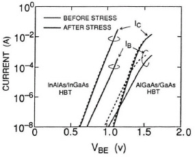
FIGURE 8.22 Gummel plot before and after stress (after Tanaka et al., Ref. 29 © IEEE).
The MOCVD devices had unstressed 200°C values of current gain of 34.3 and 36.2 for emitter–base spacing LEB= 0.5 and 2 μm, respectively. The GSMBE device had a current gain of 39.6. Unstressed turn-on voltage at 200°C was 0.806 V for the MOCVD devices and 0.834 V for the GSMBE device. Base sheet resistances were 189 and 218 Ω/sq, respectively. When stress is applied, the MOCVD devices show an initial burn-in during which current gain rises by about 5%, followed by an exponential-like decrease to about 85% of the starting value, regardless of emitter–base spacing. The GSMBE device, however, shows no significant degradation. After 40 hours of stress, the current gain at IC = 1 × 10⁴ A/cm2 changes by about 1% from the unstressed value. Similarly, the turn-on voltage increases about 9 m V for the MOCVD devices while remaining fairly stable for the GSMBE device. A larger emitter–base turn-on voltage could arise either from an increase in base doping, or the diffusion of the base dopant into the emitter. The latter effect, however, should not result in a decrease in base resistance, while the former effect should.
The presence of hydrogen in the epi is suspected when the base doping changes, since it is known that hydrogen passivates carbon acceptors [32]. The MOCVD epi has more in-grown hydrogen than the GSMBE epi, as shown by a SIM analysis result in Fig. 8.23. For the MOCVD epi, hydrogen concentrations of 1.25 × 1019 cm−3 and 1.07 × 1019 cm−3 were measured at sputter rates of 14 and 25.1 Å/s, respectively. In contrast, the GSMBE epi at a sputter rate of 14 Å/s showed a hydrogen concentration of 2.65 × 1018 cm−3 in the base; about five times lower than that obtained at the same sputter rate for the MOCVD-grown epi.
Since the MOCVD-grown epi has a high concentration of in-grown hydrogen, a substantial number of C-acceptors in the base are neutralized by the formation of C–H complexes. During stresses, the hydrogen is freed up and diffuses out of the intrinsic base region, thereby increasing the effective base doping. This hypothesis is supported by the experimental data in [32]. Since hydrogen moves out of the intrinsic base, the intrinsic base resistance will decrease, whereas the extrinsic base will remain largely unchanged. Therefore, for a given emitter area, the decrease in base resistance should be roughly independent of emitter–base spacing. The data in [32] show that the base resistance drops by 1.7Ω for MOCVD-grown devices with both LEB = 0.5 and 2 μm, in agreement with this expectation. The decrease in current gain and increase in turn-on voltage should be independent of emitter–base spacing also, assuming that the surface recombination in the extrinsic base is negligible. The data show that current gain for both device types degrades about 20% and that turn-on voltage increases about 7 mV after burn-in.
Using Fermi–Dirac statistics, Bahl et al. [31] estimated that an 8.6% increase in base doping without the effects of bandgap narrowing would correspond to a 7-mV increase in turn-on voltage. The base resistance of the MOCVD-grown device (LEB = 0.5 μm) dropped by 5.8%, which is not unrealistic for an 8.6% increase in base doping. In contrast, the GSMBE-grown device showed a 1.5% increase in base resistance and a 1-mV increase in turn-on voltage after burn-in. The results above are all consistent with dopant activation caused by hydrogen out-diffusion from the MOCVD-grown device during stress.

FIGURE 8.23 Hydroden concentration versus depth for MOCVD and GSMBE epi from SIMS analysis (after Bahl et al., Ref. 31 © IEEE).
To summarize the analysis, C-doped base InGaP/GaAs HBTs grown by MOCVD had a hydrogen concentration in the base of 8.4 × 1018 cm−3, about 20% of the base doping. During reliability testing, a medium-term degradation in current gain, a reduction in base resistance, and an increase in turn-on voltage were observed. The extrapolated activation energy of 0.64 eV is consistent with hydrogen movement in GaAs. The change in electrical characteristics is consistent with the base becoming more heavily doped as a result of C-acceptor activation due to hydrogen depassivation. In contrast, GSMBE-grown epi had five times less hydrogen concentration in the base, and HBT electrical characteristics were relatively stable under stress.
8.3 HOT CARRIER BEHAVIOR
As the dimensions of semiconductor devices shrink and the internal field rise, a large fraction of carriers in the active regions of the device are in states of high kinetic energy. At a given point in space and time, the velocity distribution of carriers may be narrowly peaked, in which case one speaks about “ballistic” electron packets. The term hot electron implies a nonequilibrium ensemble of high-energy carriers which have effective electron temperatures higher than the lattice temperature.
Ballistic motion of electrons can be launched by an electric field, thermionic emission from a wider-gap material, or tunneling. In the ballistic devices, electrons are injected into a narrow base layer at a high initial energy in the direction normal to the plane of the layer. Performance of these devices is limited by various energy-loss mechanisms in the base and by the finite probability of a reflection at the base–collector barrier. For example, electrons of HBTs are tunnel injected from the emitter to the conduction-band of the p-type quasi-neutral base. Initially, the injected electrons have average excess kinetic energy. At first the electron momentum is predominantly in the x direction (i.e., perpendicular to the plane of the injector). Later, while traversing the base, the injected electron can experience elastic (impurity) and inelastic collisions. This results in a redistribution of kinetic energy and directional motion. After transiting the base, electrons impinge on the collector barrier. The energy of this barrier may be controlled by the collector–base voltage. Derivation of the collector current with respect to the collector–base voltage for the AlGaAs/GaAs HBT is sketched in Fig. 8.24. The upper curve of this plot represents the initial energy of 220 meV and the lower curve represents the initial energy of 170 meV. The HBT has a p-type GaAs base with a concentration of 3 × 1018 cm−3 and a base thickness of 260 Å. d IC/dVCB as a function of VCB gives information related to a projection of the electron momentum distribution perpendicular to the plane of the collector barrier. Hot electron spectroscopy has been used to demonstrate the existence of nonequilibrium electron transport in the base of an AlGaAs/GaAs HBT in which the base width is comparable to the electron mean free path. In general, hot-electron HBTs show both high-gain and exceptionally high-speed operation.

FIGURE 8.24 Derivation of the collector current dIC/dVCB as a function of VCB (after Berthod et al., Ref. 33 © American Institute of Physics).
The hot electrons, which introduce the current gain degradation, are those injected into the Si/SiO2 interface of Si and SiGe bipolar transistors. Degradation of the bipolar current gain under emitter–base junction reverse-bias stress has been investigated extensively in the past decade [34–39]. It was believed that the current gain degradation was due to stress-generated interface traps at the oxide-covered emitter–base junction space-charge region. These interfacial traps were thought to be due to the dangling bonds from ruptured weak bonds during hot electron impact. Higher interface trap density gives higher electron–hole recombination rate, larger base current, and lower current gain via the SRH recombination current in the p-n junction space-charge region.
Figure 8.25 shows an n+-p junction and its energy-band diagram under reverse-bias stress. Under the oxide there are interface traps DIT (open triangles) at weak bonds (filled triangles) and charging of oxide electron (open squares) and hole (open hexagons) traps QOT by hot electrons and hot holes. Since the only direct source of hot electrons in n-p-n bipolar transistors under emitter–base reverse-bias stress is the thermal emission of trapped electrons, these thermal electrons are accelerated to high kinetic energies by the applied emitter–base voltage. The thermal emission rate increases rapidly with increasing temperature. Examine the measured base currents taken at 77 and 298 K shown in Fig. 8.26. The stress-induced base current increments are not a strong function of temperature. This indicates that thermally activated hot electrons are not the dominant hot carriers in a reverse-bias emitter–base junction. Because of the very high base and emitter doping concentrations, the emitter reverse current should be dominated by tunneling, such as tunneling of the valence-band electrons in the p-base into the unoccupied conduction-band states. This tunneling occurs predominately at the highest electric field location near the n+/p dopant-compensation boundary of the emitter–base junction. The tunneling is consistent with the small temperature dependence observed in Fig. 8.26. The tunneled valence-band electron labeled by the circled dots next to (T) leaves a thermal hole in the valence band of the emitter space-charge region. This thermal hole (the circles with the dot removed or electron dot tunneling out to the n+ emitter’s conduction-band) is then accelerated by the applied VEB-stress, moving in parallel with and adjacent to the SiO2/Si interface toward the p-base boundary of the emitter–base SCR at the SiO2/Si interface. This accelerated and hot primary hole can then generate secondary hot electrons by intervened impact generation.
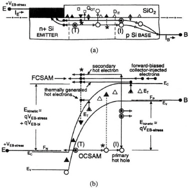
FIGURE 8.25 Thermally generated hot electrons, primary hot holes, and secondary hot electrons in (a) the cross sectional view and (b)the energy-band diagram along the SiO2/Si interface (after Neugroschel et al., Ref. 40 © IEEE).
Kizilyalli and Bude [41] used Monte Carlo simulations to determine the hot-electron and hot-hole distributions in the EB junction at high kinetic energies or stress voltages. The current gain degradation due to both the primary hot holes and secondary hot electrons was suggested. Neugroschel et al. [42] demonstrated experimental evidence of the degradation of current gain during reverse emitter–base bias stress. Experimental data favor the primary hot-hole pathways over secondary hot-electron pathways. The experimental stress fluence, charge to failure (QTF), was computed by QEB-stress = ∫ jE-stress (t)dt, for a 10% drop in current gain measured at VBE = 0.8 V. Figure 8.27a shows QTF versus VEB-stress for the two stress-and-measure (SAM) experiments [42] that delineated the hot-electron and hot-hole contributions. In Fig. 8.27a the circles represent the data from the open-collector or reverse-collector bias SAM bias configurations encountered in normal BiCMOS circuit operations in which both the primary hot-hole and secondary hot-electron degradation pathways could contribute. The solid lines represent the data from forward-biased collector–base junction SAM measurements (FCSAM) in which the hot-electron current injected by the forward-biased collector–base junction.

FIGURE 8.26 Collector and base currents versus base–emitter voltage (after Neugroschel et al., Ref. 40 © IEEE).
The fundamental parameter of DIT generation is the hot carrier kinetic energy, not VEB-stress; thus the kinetic energy of the primary holes in the OCSAM experiment is about EG+ EFn+ smaller than that in the FCSAM experimental, which accounts for the 1.23-V negative lateral shift of the FCSAM data from the OCSAM in Fig. 8.27a. Because only a small fraction of the electrons injected by the forward-biased collector–base junction in the FCSAM experiment will flow in the electron surface channel next to the SiO2–Si interface at the EB junction perimeter to break the weak bonds and increase DIT, the collector–base forward-bias voltage must be large, which gives high IC and IE values in the bulk region of the base layer. This large bulk component shifted the QTF(FCSAM) data upward from the OCSAM data by about 6.05/6.47 × 10−3 ≈ 935, as indicated in the QTF–Ek−max plot in Fig. 8.27b. The nearly constant QTF ratio of the OCSAM and FCSAM data indicates that the primary hot holes dominate over secondary hot electrons under the open- and reverse-bias collector-circuit-operation bias configurations and that the nearly identical kinetic energy dependence of the generation efficiency of interface traps is initiated by tunnel-injected hot holes and substrate-injected hot electrons. Using the normalized FCSAM and OCSAM experimental data, time to failure (TTF = QTF/JE-stress) versus VEB-stress is displayed in Fig. 8.28. The curve gives 2.35 V for the 10-year-TTF maximum operation voltage.

FIGURE 8.27 QTF versus (a) VEB-stress and (b) Ek-max (after Neugroschel et al., Ref. 42 © IEEE).
The base current relaxation transient following reverse emitter–base bias stress was measured in silicon bipolar transistors [43]. Figure 8.29 shows IB versus time measured at VBE-mess = 0.56 V during relaxation for a self-aligned bipolar transistor after reverse-bias stress at various stress voltages. The device was previously stressed at VEB-stress = 4.5 V for 104 s. The inset in Fig. 8.29 shows IB versus stress time. The base current increases with an increase in the stress time. In the IB relaxation transient measurement, the base current decreases with time. The poststress IB relaxation measured in the forward-biased EB junction results from the discharging of oxide traps. The oxide trap charging and discharging rates are determined by the trap distribution in the oxide rather than by the EB-junction perimeter electric field that controls the IB degradation due to NIT generation by hot carriers during reverse-bias stress. Device temperature as a factor affecting the IB relaxation characteristics is ruled out because the collector current remained constant during IB relaxation transient measurements.

FIGURE 8.28 TTF versus VEB-stress (after Neugroschel et al., Ref. 42 © IEEE).

FIGURE 8.29 IB versus time (after Neugroschel et al., Ref. 43 © IEEE).
The analysis in [43] shows that the IB relaxation is due to trapped holes in the oxide tunneling to the silicon valence band. The measured dependence of the IB relaxation on time, temperature, stress voltage, and forward bias during relaxation all support the hole tunneling mechanism. Since the delay time of ≈ 1 ms for IB relaxation to begin after termination of reverse-bias stress was observed, the bipolar reliability in high-speed circuits can be determined by measuring IB within ≈ 1 ms after stress.
8.4 RADIATION EFFECTS
Semiconductor devices in space radiation and nuclear explosion environments can suffer crystalline lattice displacement (defects) and ionization (generation of electron–hole pairs) effects. Radiation effects are generally divided into four categories according to their sources: (1) total ionizing dose, (2) neutron, (3) dose rate (low and high), and (4) single-event upset (SEU). The displacement alters the device performance by reduction of minority-carrier lifetime, majority-carrier removal (trapping and compensation), and mobility degradation. The ionization interaction in a low-dose-rate environment causes gradual charging of dielectric regions, while a high-dose-rate environment causes transient photocurrents. Dose-rate effects could upset circuit functions and cause burnout of junctions or interconnections associated with high or multiplied photocurrents. High-energy galactic particles, protons, and solar flare ions are the main sources of SEU in space, while alpha particles from minute traces of radiotopes in ceramic chip packages can cause the same effect in non-space-based environments. Excess carriers generated by these heavily ionizing particles incident on sensitive junctions are collected to create subnanosecond current pulses. Circuit upsets can result from a single particle confined to a single node. In some cases, single-event currents are regeneratively amplified in a device to cause burnout. Radiation-intensive applications include satellite systems, high-energy particle accelerators, instrumentation in nuclear reactors, and many low-noise high-speed military systems.
Radiation introduces point defects such as vacancies, interstitial, and antisites in semiconductors. Various materials respond differently to the same radiation environment because of variations in the formation of radiation-induced lifetime-limiting defects. In Si, radiation-induced point defects interact with dopants to form lifetime-limiting traps, resulting in higher lifetime degradation with increased base doping concentration [44]. In InP some of the radiation-induced point defects interact with the dopants to form complexes that do not affect the lifetime [45]. This results in a lower net concentration of radiation-induced lifetime-limiting point defects in InP. Consequently, an increase in doping concentration results in a decrease in the lifetime degradation in InP. Unlike Si and InP, the radiation-induced point defects in GaAs do not interact appreciably with the dopants, resulting in only a weak dependence of lifetime degradation on base doping. In GaAs, lifetime-limiting defects are attributed directly to point defects, such as antisites or sublattice atom vacancies [46].
Figure 8.30 shows the calculated lifetime as a function of doping concentration for Si, GaAs, and InP after a 1-MeV electron irradiation at a fluence of 1 × 1015 cm−3. Based on limited experimental data, radiation effects on SiGe HBTs are known as similar to that of Si bipolar transistors. The radiation hardness of GaAs HBTs are significantly greater than Si bipolar transistors, and InP-based HBTs are more radiation hard than are GaAs/AlGaAs HBTs.
8.4.1 Si-Based Bipolar Transistors
The detrimental effects of ionizing radiation on conventional double-diffused silicon bipolar transistors are well known. There has been renewed interest in the effects of ionizing radiation on modem double polysilicon self-aligned BJTs. Bipolar transistors are susceptible to particle bombardment in radiation environments, which create trapping centers in the emitter–base space-charge region and the base region and therefore increase electron–hole recombination in these regions [48]. For SiGe heterojunction bipolar transistors, however, very few radiation experimental data have been reported. Babcock et al. [49] reported in 1995 the effect of ionizing radiation on both the electrical and 1/f noise characteristics of advanced UHV/CVD SiGe HBTs for the first time. High-performance SiGe HBTs and Si BJTs manufactured by IBM were used in their investigation [50]. To ensure unambiguous comparison, the Si BJTs were processed in the same wafer lot, under processing conditions identical to those for SiGe HBTs. The only difference was the growth of Ge in the epitaxial base. Transistors were fabricated using a planar structure with a conventionally doped arsenic polysilicon emitter and a deep-trench isolation process, which is believed to give these transistors an inherent tolerance to ionizing radiation.
Irradiation was performed in a Gamma-Cell with a 60Co source providing a dose rate of about 48 rad(Si)/s. Pre- and postradiation electrical measurements were made after devices were removed from the source at 300 K using a computer-controlled Keithley measurement system. Delay time between irradiation and remote testing was approximately 15 minutes. All device terminals were grounded during irradiation and the dose rate during irradiation was confirmed using TLD dosimeters. Pre- and postradiation low-frequency 1/f noise measurements were made using an HP 3561 dynamic signal analyzer.

FIGURE 8.30 Calculated lifetime of Si, GaAs, and InP versus base doping concentration (a) before and (b) after irradiation (after Augustine et al., Ref. 47 © IEEE).

FIGURE 8.31 (a) IC and IB and (b) current gain versus VBE (after Babcock et al., Ref. 49 © IEEE).
The typical response of a SiGe HBT to ionizing radiation is displayed in the Gummel and β plots in Fig. 8.31a and b, respectively. As shown in Fig. 8.31a, ionizing radiation causes an increase in base current at low base–emitter voltages but does not affect the collector current of the SiGe HBT. Pre- and postradiation current gain in Fig. 8.31b indicate the reduction of current gain at low base–emitter voltages. A similar response to ionizing radiation was also observed in the electrical characteristics of Si BJTs. Radiation exposure to 2.0 Mrad(Si) results in virtually no current gain degradation for VBE ≥ 0.8 V (JC ≈ 24 μA/μm2 in the SiGe HBT). For VBE < 0.8 V, degradation in the current gain of both the SiGe HBT and the Si BJT becomes significant, especially for low base–emitter voltages. Less than 8% shift in the peak current gain (VBE = 0.7 V) after exposure to 2 Mrad(Si) has been observed. These results are remarkable compared to modern Si bipolar transistors, which typically have a 50% or greater reduction in the peak current gain after exposure to 500 krad(Si) [51]. Enhanced tolerance of the UHV/CVD SiGe HBTs and the Si BJTs used in the investigation is believed to be due to the result of the thin nitride/oxide spacer and the high doping at the surface of the epi base region. Utilization of a thin nitride/oxide spacer region over the intrinsic base results in significant reduction in the radiation-induced oxide trapped charge and interface trapped charge over conventional SiO2 spacers. UHV/CVD growth of the epitaxial base region allows for the incorporation of dopant atoms during the growth phase and thus eliminates implant damage in the screen oxide, which is typically found in more conventional bipolar processes [52]. The high doping at the surface of the epi base region requires a proportionally larger amount of radiation-induced trapped charge to cause a parasitic inversion region to form when compared to a lower-doped base.
Figure 8.32 shows the percent change in normalized base current difference (Δ IB/IB) versus total radiation dose at constant VBE. ΔIB is the difference between the post- and preradiation base current. In Fig. 8.32, almost identical shifts in base current with total radiation dose for both the SiGe HBT and the Si BJT have been observed. These results suggest that the introduction of SiGe strained layers into the epitaxial base of the SiGe HBT do not impose any additional reliability risk for ionizing radiation tolerance compared to Si BJTs.
The flicker noise of SiGe HBTs before and after ionizing radiation was measured [49]. Exposure to ionizing radiation resulted in an observed increase in the I/f noise in several of the SiGe HBTs and Si BJTs investigated. Figure 8.33 shows the measured pre- and postradiation equivalent base noise power spectral densities (SIB) in a SiGe HBT after exposure to 2 Mrad(Si). An increase in the 1/f noise is apparent after irradiation. The multiplication of SIB by the frequency reveals a Lorentzian-shaped hump superimposed on the 1/f component which is associated with generation–recombination (G/R) centers [53]. The time constant associated with G/R centers contributing to the postradiation noise is found by taking 1/ωG/R ≈ 6.1 ms, where ωG/R = 2πfG/R and fG/R is the 3-dB break frequency associated with the G/R noise (26Hz in this case).

FIGURE 8.32 Percent change in base current versus total dose (after Babcock et al., Ref. 49 © IEEE).

FIGURE 8.33 Equivalent base noise power spectral density (SIB) versus frequency before and after ionizing radiation (after Babcock et al., Ref. 49 © IEEE).
8.4.1.1 Oxide Trapped Charge and Excess Base Current
Exposure to ionizing radiation degrades the current gain of bipolar transistors by increasing the base current while leaving the collector current approximately unchanged, as evidenced by the Gummel plot in Fig. 8.33 [54]. The role of the net positive oxide trapped charge and surface recombination velocity on excess base current is identified. The oxide charge changes the surface potential along the base surface, causing depletion in the n-p-n bipolar transistor. The interface states near midgap cause an increase in the surface recombination velocity. Because of the surface potential behavior, the effects of ΔNot and ΔNit on ΔIB are interactive and not simply additive. In addition, the defects of interest in BJTs are not precisely the same as those in MOS transistors. For example, ΔNit in MOSFETs is a measure of the number of charged interface states at threshold. In BJTs, on the other hand, the excess base current depends on the number of interface states (recombination centers) near midgap, not the total number between midgap and threshold. The excess base currents due to changes in surface potential depend on the total radiation-induced oxide charge at the bias condition and the lateral position of interest
Consider the IB curves in Fig. 8.34, which exhibit two distinct slopes. The slope corresponding to the ideality factor 1 < n < 2 is a clear indication that surface recombination near the junction is dominant. The transition to n = 2 at higher values of VBE is a signature of predominately bulk rather than surface recombination. The voltage at which this transition occurs is an indication of the amount of radiation-induced charge in the oxide covering the emitter–base junction and the intrinsic base.

FIGURE 8.34 Base and collector currents versus base–emitter voltage at various radiation levels (after Kosier et al., Ref. 54 © IEEE).
8.4.1.2 Low-Dose-Rate Radiation
Investigations of the total dose response of modem n-p-n bipolar transistors have shown that the gain degradation is much greater at a dose rate below 10 rad/s than at a dose rate above 100 rad/s. Recent analysis of low-dose-rate response shows that excess base current, oxide charge, and effective surface recombination velocity are highest at a lower dose rate (< 10 rad/s) and decrease with increasing dose rate until they become independent of dose rate at higher dose rates (> 100 rad/s). The dose-rate response of the BJT is very different from the dose-rate response of MOSFETs [55], where oxide charge tends to be reduced at low dose rates due to trapped-hole neutralization and/or interface trap buildup. The enhanced degradation at low dose rate is a result of a larger net trapped positive charge NOX in base oxides at low electric field [52]. This larger NOX (20 to 30% higher) can cause a much larger (5 to 10 times) value of excess base current ΔIB when the surface potential at the intrinsic base surface is near the crossover point.

FIGURE 8.35 Normalized excess base current versus dose rate (after Nowlin et al., Ref. 55 © IEEE).
Figure 8.35 shows dose-rate dependence of the normalized excess base current for devices irradiated at room temperature. The magnitude of the total-dose-induced excess base current is independent of dose rate above 150 rad(SiO2)/s, and it increases below 150 rad(SiO2)/s. The degradation at low dose rates is about three to four times greater than that at the high dose rates. Moreover, these results are relatively independent of irradiation source.
The implications for radiation hardness assurance are discussed as follows. Since the dose-rate response saturates at low dose rates, it is not necessary to test at even lower dose rates to determine the device response for space applications because of the cost and time required for low-dose-rate experiments. One may have to test at dose rates about three- to fourfold worse than the high-dose-rate response when these devices are exposed to 100 krad(SiO2)/s. An overtest in dose by a factor of 3 can allow one to conservatively estimate device suitability for space applications if other circuit elements do not interfere by causing earlier failure.
8.4.1.3 Implications for Circuit Behavior
The total dose-rate radiation affects the input offset voltage, input offset current, and open-loop gain of linear amplifiers [56]. At a low dose rate, the average input offset voltage increases to −11 mV at 100 krad, whereas at high dose rate, the average showed essentially little change in Fig. 8.36a. Following a 168-hour 25°C anneal, the high-dose-rate average increased to −1.5 m V, then decreased slightly after an additional 300-hour l00°C anneal. Thus the change in input offset voltage at low dose rate is much greater than the change at high dose rate plus anneal. The input offset current increases significantly with total dose for both low and high dose rates, as shown in Fig. 8.36b. In Fig. 8.36c the open-loop gain decreases with total dose. The degradation is enhanced for low dose rate.
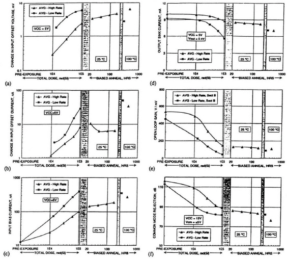
FIGURE 8.36 Change in (a) input offset voltage, (b) input offset current, (c) input bias current, (d) output sink current, (e) open-loop gain, and (f) common-mode rejection ratio versus total dose and anneal hours of a BJT linear amplifier (after McClure et al., Ref. 56 © IEEE)
Analog-to-digital converters (ADCs) are sensitive to the total ionizing dose. The most sensitive parameters were transfer curve nonlinearities, reference voltage, and tristate leakage current. The converters failed functionally at lower dose level with the low-dose-rate testing. After total dose irradiation, the internal reference voltage degraded significantly. The internal track-and-hold amplifier on the analog input allows the converter to accurately convert an input sine wave of 6 V peak-to-peak amplitude accuracy. Noise in this critical path along with internal reference noise will add significant distortions to the input sine wave and will eventually degrade the dynamic performance of the converter. The harmonic distortion of the converter increases substantially as the total dose radiation level increases. The signal-to-noise ratio decreases significantly as the noise level and number of harmonics increases. Similar noise results for a low-noise amplifier after total dose irradiation were observed. The voltage noise of this device was essentially unchanged by radiation, but the current noise degraded severely.
8.4.2 GaAs- and InP-Based Bipolar Transistors
To date, there has been little work on radiation effects on III/V compound HBTs. Schrantz et al. [57] reported that AlGaAs/GaAs HBTs irradiated with 1015 neutrons/cm−2 demonstrated much higher levels of immunity than did Si bipolar transistors. Devices fabricated from III/V materials generally display more resistance to total dose effects from all forms of radiation than does a comparable Si-based structure. The greater radiation hardness of III/V compound HBTs arises from shielding of the active junctions from the semi-insulating substrate by the highly doped sub-collector layer. Also, there is no n-p isolation junction effects or Fermi-level pinning at the surface. GaAs/AlGaAs heterojunction inverted transistor integrated logic gate arrays proved to be relatively insensitive to energetic protons and heavy ions between 37 and 66 meV.
Yamaguchi and co-workers [58–61] studied p-type InP with a report of 1.0-MeV electron irradiation-induced electron traps at activation energies of EA = 0.15, 0.22, 0.2, 0.37, and 0.52 eV and an electron trap at EA = 0. 19 eV. They attribute the radiation resistance of InP to the migration energy of In- and P-displaced atoms in InP, which is favorable compared to GaAs. Sibille et al. [62,63] reported on 1.0-MeV electron irradiation of p-InP using a Ti–Au Schottky contact. They reported hole traps with EA = 0.17, 0.33, 0.37, and 0.54 eV, in good agreement with Yamaguchi, although capture cross section differed in some cases by an order of magnitude. Sibille observed a significant reduction in radiation damage by annealing at 470 K for 10 min. They also identified the 0.37-eV level as a point defect and the 0.52-eV level as a point defect-impurity complex.
8.4.2.1 Total Dose Effects
In total dose testing a 60Co source provides gamma-ray radiation, which generates Compton electrons, accumulated over a long period. The damage is considered permanent. The total-dose environment appears to be less harmful to HBTs than to Si devices. InP-based devices are expected to be even more radiation-hard than their GaAs-based counterparts.
Song et al. [64] examined the radiation hardness of GaAs/AlGaAs HBTs in neutron, total γ-ray dose, and dose-rate environments. The HBTs were 3 × 10 μm2 devices, with Be base doping of 1 × 1019 cm−3, grown by MBE. Fission neutrons with energy greater than 10 keV were used to irradiate samples up to doses of 1.3 × 10¹⁴ neutrons/cm2. The dc gain of the devices decreased from 60 to 48 after a neutron flux of ≈ 1014 cm−2, with the onset of degradation at ≈ 3 × 1013 cm−2. It was postulated that much of the gain decrease resulted from an increase in space-charge recombination at the emitter–base heterojunction. The RF performance was unchanged by a neutron dose of 1014 cm−2. Similarly, only minor changes in dc gain of these devices was observed after a total γ-ray dose of 467 Mrad (7% reduction in current gain).

FIGURE 8.37 SEM micrographs of AlInAs/InGaAs before (a) and after (b)catastrophic failure (after Jalali and Pearton, Ref. 10 © Artech House).
Minimal changes in the dc characteristic of the InP-based HBT were observed for doses up to 20 Mrad, while at 40 Mrad some of the devices started to fail catastrophically. The failure-mode characteristic, an open circuit from base to emitter, was the same in all failed HBTs. The base-to-collector junction was not affected. The failed devices showed the presence of large quantities of oxygen and carbon-rich debris around the contact as displayed in Fig. 8.37. Parametric changes, such as decreased current gain, transconductance, and increased output resistance, were observed in the devices at high doses. Figure 8.38 shows a Gummel plot of a 2 × 4μm2 AlInAs/InGaAs HBT before and after 40-MRad radiation. Significant degradation of collector current occurs for VBE > 1.0 V, while the base current is increased at high base–emitter biases.
8.4.2.2 Transient Radiation Effects
Dose-rate tests have been performed by using flash x-ray pulses, 22 ns wide. The HBT transient collector current recovery time is on the order of a few microseconds, as shown in Fig. 8.39. The lack of long-term transients in HBTs is due to the vertical structure, where the active junctions are isolated from surfaces and substrate interface. Another transient radiation effect is the single-event upset (SEU). High-energy galactic particles, protons, and solar flare ions are the main sources of SEU in space, while alpha particles (helium nuclei) from minute traces of radioisotopes in ceramic chip packages can cause the same effect in non-space-based environments. Excess carriers generated by these heavily ionizing particles incident on sensitive junctions are collected to create a subnanosecond current pulse. In some cases, single-event currents are amplified regeneratively in a device to cause burnout. An LSI RAM or shift register is attractive for SEU monitoring.
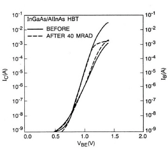
FIGURE 8.38 ICand IB of an AlInAs/InGaAs HBT before and after a 40-Mrad dose of 60Co γ-ray radiation (after Jalali and Pearton, Ref. 10 © Artech House).

FIGURE 8.39 Transient collector and base currents of an AlGaAs/GaAs HBT during a 120-ns ionizing radiation pulse (after Jalali and Pearton, Ref. 10 © Artech House).
REFERENCES
1. M. Hafizi, W. W. Stanchina, R. A. Metzger, J. F. Jensen, and F. Williams, “Reliability of AlInAs/GaInAs heterojunction bipolar transistors,” IEEE Trans. Electron Devices, ED-40, 2178 (1993).
2. M. Hafizi, W. E. Stanchina, F. Williams, Jr., and J. F. Jensen, “Reliability of InP-based HBT IC technology for high-speed, low-power applications,” IEEE Trans. Microwave Theory Tech., MTT-43, 3048 (1995).
3. R. S. Hemmert, G. S. Prokop, J. R. Lloyd, P. M. Smith, and B. M. Calabrese, “The relationship among electromigration, passivation thickness, and common-emitter current gain degradation within shallow junction npn bipolar transistors,” J. Appl. Phys., 53, 4456 (1982).
4. R. S. Hemmert and M. Costa, “Electromigration-induced compressive stresses in encapsulated thin-film conductors,” Proceedings of the 29th IEEE International Reliability Physics Symposium, 64 (1991).
5. R. A. Wachnik, T. J. Bucelot, and G. P. Li, “Degradation of bipolar transistors under high current stress at 300 K,” J. Appl. Phys., 63, 4734 (1988).
6. C. J. Sun, T. A. Grotjohn, C.-J. Huang, D. K. Reihard, and C.-C. W. Yu, “Forward-bias stress effects on BJT gain and noise characteristics,” IEEE Trans. Electron Devices, ED-41, 787 (1994).
7. C. J. Sun, D. K. Reinhard, C.-J. Huang, T. A. Grotjohn, and C.-C. W. Yu, “Hot-carrier-induced degradation and post-stress recovery of bipolar transistor gain and noise characteristics,” IEEE Trans. Electron Devices, ED-39, 2178 (1992).
8. A. Neugroschel, C.-T. Sah, J. M. Ford, J. Steele, R. Tang, and C. Stein, “Comparison of time-to-failure of GeSi and Si bipolar transistors,” IEEE Electron Device Lett., EDL-17, 211 (1996).
9. M. Hong, E. de Frésart, J. Streele, A. Zlotnicka, C. Stein, G. Tam, M. Racanelli, L. Knoch, Y.-C. See, and K. Evans, “High-performance SiGe epitaxial base bipolar transistors produced by a reduced-pressure CVD reactor,” IEEE Electron Device Lett., EDL-14, 450 (1993).
10. B. Jalali and S. J. Pearton, eds., InP HBTs: Growth, Processing, and Applications, Artech House, Norwood, MA (1995).
11. M. Hafizi, T. Liu, A. E. Schmitx, P. A. McDonald, M. Lui, and F. Williams, “Power performance and reliability of AlInAs/GaInAs/InP double heterojunction bipolar transistors,” Proceedings of the 6th International Conference on InP and Related Materials, Santa Barbara, CA, 527 (1994).
12. J. J. Liou and C. I. Huang, “Base and collector currents of pre- and post-burn-in AlGaAs/GaAs heterojunction bipolar transistors,” Solid-State Electron., 37, 1349 (1994).
13. J. L. Benton, M. Levinson, A. T. Macrander, H. Temkin, and L. C. Kimberling, “Recombination enhanced defect annealing in n-InP,” Appl. Phys. Lett., 45, 566 (1984).
14. H. Sugahara, J. Nagano, R. Nittono, and K. Ogawa, “Improved reliability of AlGaAs/GaAs heterojunction bipolar transistors with a strain-relaxed base,” IEEE GaAs IC Symposium, 115 (1993).
15. M. Borgarino, R. Plana, J. G. Tartarin, S. Delage, H. Blanck, F. Fantini, and J. Graffeuil, “On the stability of the DC and RF gain of GaInP/GaAs HBTs,” 1996 Workshop on High Performance Electron Devices for Microwave and Optolectronic Applications, 37 (1996).
16. M. Borgarino, J. G. Tartarin, S. Delage, R. Plana, F. Fantini, and J. Graffeuil, “Correlation between the burn-in effect and the extrinsic base surface quality in C-doped GaInP/GaAs HBTs,” 1997 Workshop on High Performance Electron Devices for Microwave and Optolectronic Applications, 43 (1997).
17. E. J. Prinz, P. M. Garone, P. V. Schwartz, X. Xiao, and J. C. Sturm, “The effects of base dopant out-diffusion and undoped Si1−xGex, junction spacer layers in Si/Si1−xGex/Si heterojunction bipolar transistors,” IEEE Electron Device Lett., EDL-2, 42 (1991).
18. F. M. Yamada, A. K. Oki, D. C. Steet, Y. Saito, D. K. Umemoto, L. T. Tran, S. Bui, J. R. Velebir, and G. W. Mclver, “Reliability analysis of microwave GaAs/AlGaAs HBTs with beryllium and carbon doped base,” Dig. IEEE MTT, 739 (1992).
19. R. People and J. C. Bean, “Band alignment of coherently strained GexSi1x−/Si heterostructure on ![]() 00
00![]() GeySi1−y substrates,” Appl. Phys. Lett., 48, 538 (1986).
GeySi1−y substrates,” Appl. Phys. Lett., 48, 538 (1986).
20. R. Fair, “Boron diffusion in silicon: concentration and orientation dependence, background effects and profile estimation,” J. Electrochem. Soc., 122, 800 (1975).
21. D. L. Miller and P. M. Asbeck, “Be redistribution during growth of GaAs and AlGaAs by molecular beam epitaxy,” J. Appl. Phys., 57, 1816 (1985).
22. O. Nakajima, H. Ito, T. Nittono, and K. Nagata, “Current induced degradation of Be-doped AlGaAs/GaAs HBTs and its suppression by Zn diffusion into extrinsic base layer,” IEDM Tech. Dig., 673 (1990).
23. A. Gruhle, “The influence of emitter–base junction design on collector saturation current, ideality factor, Early voltage, and device switching speed of Si/SiGe HBTs,” IEEE Trans. Electron Devices, ED-41, 198 (1994).
24. J. W. Slotboom, G. Streutker, A. Pruijmboom, and D. Gravesteijn, “Parasitic energy barriers in SiGe HBTs,” IEEE Electron Device Lett., EDL-12, 486 (1991).
25. R. People and J. C. Beam, “Band alignments of coherently strained GeSi/Si heterostructures,” Appl. Phys. Lett., 48, 538 (1986).
26. K. Zhang, X. Zhang, P. Bhattacharya, and J. Singh, “Influence of psedomorphic base–emitter spacer layers on current-induced degradation of beryllium-doped InGaAs/InAlAs heterojunction bipolar transistors,” IEEE Trans. Electron Devices, ED-43, 8 (1996).
27. H. Ito, O. Nakajima, T. Furuta, and J. S. Harris, Jr., “Influence of dislocations on the dc characteristics of AlGaAs/GaAs heterojunction bipolar transistors,” IEEE Electron Device Lett., EDL-13, 232 (1992).
28. H. Ito, T. Furuta, and T. Ishibashi, “Minority electron lifetimes in heavily doped p-type GaAs grown by molecular beam epitaxy,” Appl. Phys. Lett., 58, 2936 (1991).
29. S. Tanaka, K. Kasahara, H. Shimawaki, and K. Honjo, “Stress current behavior of InAlAs/InGaAs and AlGaAs/GaAs HBTs with polyimide passivation,” IEEE Electron Device Lett., EDL-13, 560 (1992).
30. M. Hafizi, R. A. Metzger, and W. E. Stanchina, “Stability of beryllium-doped compositionally graded and abrupt AlInAs/GaInAs HBTs,” Appl. Phys. Lett., 63, 93 (1993).
31. S. R. Bahl, L. H. Camnitz, D. Houng, and M. Mierzwinski, “Reliability investigation of InGaP/GaAs heterojunction bipolar transistors,” IEEE Electron Device Lett., EDL-17, 446 (1996).
32. S. J. Peart on, C. R. Abernathy, and J. W. Lee, “Comparison of H+ and He+ implant isolation of GaAs-based heterojunction bipolar transistors,” J. Vac. Sci. Technol., B13, 15 (1995).
33. K. Berthod, A. F. J. Levi, J. Walker, and R. J. Malik, “Extreme nonequilibrium electron transport in heterojunction bipolar transistors,” Appl. Phys. Lett., 52 (26), 2247 (1988).
34. D. R. Collins, “Excess current generation due to reverse bias P-N junction stress,” Appl. Phys. Lett., 14, 264 (1968).
35. D. D. Tang and E. Hackbarth, “Junction degradation n bipolar transistors and the reliability imposed constraints to scaling and design,” IEEE Trans. Electron Devices, ED-35, 2101 (1988).
36. J. D. Burnett and C. Hu, “Modeling hot carrier effects in polysilicon emitter bipolar transistors,” IEEE Trans. Electron Devices, ED-35, 2238 (1988).
37. D. Quon, P. K. Gopi, G. J. Sonet, and G. P. Li, “Hot carrier induced bipolar transistor degradation due to base dopant compensation by hydrogen: theory and experiment,” IEEE Trans. Electron Devices, ED-41, 1824 (1994).
38. H. S. Momose and H. Iwai, “Analysis of the temperature dependence of hot-carrier-induced degradation in bipolar transistors for BiCMOS,” IEEE Trans. Electron Devices, ED-41, 978 (1994).
39. S. L. Kosier, A. Wei, R. D. Schrimpf, D. M. Fleetwood, M. D. DeLaus, R. L. Pease, and W. E. Combs, “Physically based comparison of hot-carrier-induced and ionizing-radiation-induced degradation in BJTs,” IEEE Trans. Electron Devices, ED-42, 436 (1995).
40. A. Neugroschel, C.-T. Sah, and M. S. Carrol, “Degradation of bipolar transistor current gain by hot holes during reverse emitter–base bias stress,” IEEE Trans. Electron Devices, ED-43, 1286 (1996).
41. I. C. Kizilyalli and J. D. Bude, “Degradation of gain in bipolar transistors, ” IEEE Trans. Electron Devices, ED-41, 1083 (1994).
42. A. Neugroschel, C. T. Sah, and M. S. Carrol, “Accelerated reverse emitter–base stress methodologies and time-to-failure applications,” IEEE Electron Device Lett., EDL-17, 112 (1996).
43. A. Neugroschel, C.-T. Sah, M. S. Carrol, and K. G. Pfaff, “Base current relaxation transient in reverse emitter–base stressed silicon bipolar junction transistors,” IEEE Trans. Electron Devices, ED-44, 792 (1997).
44. A. Rohatgi, “Radiation tolerance of boron doped dendritic web silicon solar cells,” 4th Solar Cell High Efficiency and Radiation Damage Conference, Cleveland, OH, 281 (1980).
45. M. Yamaguchi and K. Ando, “Effects of impurities on radiation damage in InP,” J. Appl. Phys., 60, 935 (1986).
46. D. Pons, A. Mircea, and J. Bourgoin, “An annealing study of electron irradiation-induced defects in GaAs,” J. Appl. Phys., 51, 4150 (1980).
47. G. Augustine, A. Rohatgi, and N. M. Jokerst, “Base doping optimization for radiation-hard Si, GaAs, and InP solar cells,” IEEE Trans. Electron Devices, ED-39, 2395 (1992).
48. J. J. Liou, J. S. Yuan, and H. Shakouri, “Modulating the bipolar junction transistor subjected to neutron irradiation for integrated circuit simulation,” IEEE Trans. Electron Devices, ED-39, 593 (1992).
49. J. A. Babcock, J.D. Cressler, L. S. Vempati, S. D Clark, R. C. Jaeger, and D. L. Harame, “Ionizing radiation tolerance and low-frequency noise degradation in UHY/CYD SiGe HBTs,” IEEE Electron Device Lett., EDL-16, 351 (1995).
50. D. L. Harame, J. M. C. Stork, B.S. Meyerson, K. Y. Hsu, J. Cotte, K. B. W. Scharf, and J. A. Yasaitis, “Optimization of SiGe HBT technology for high speed analog and mixed-signal applications,” IEDM Tech. Dig., 874 (1993).
51. R. N. Enlow, R. L. Pease, W. E. Combs, R. D. Schrimpf, and R. N. Nowlin, “Response of advanced bipolar process to ionizing radiation,” IEEE Trans. Nucl. Sci., NS-39, 2206 (1992).
52. D. M. Fleetwood et al., “Physical mechanisms contributing to enhanced bipolar gain degradation at low dose rates,” IEEE Trans. Nucl. Sci., NS-41, 1871 (1994).
53. Y. Dai, “Deep-level impurity analysis for p-n junctions of a bipolar transistor from low-frequency G-R noise measurements,” Solid-State Electron., 32, 439 (1989).
54. S. L. Kosier, R. D. Schrimpf, R.N. Nowlin, D. M. Fleetwood, M. DeLaus, R. L. Pease, W. E. Combs, A. Wei, and F. Chai, “Charge separation for bipolar transistors,” IEEE Trans. Nucl. Sci., NS-40, 1276 (1993).
55. R.N. Nowlin, D. M. Fleetwood, and R. D. Schrimpf, “Saturation of the dose-rate response of single-poly BJTs below 10 rad(SiO2)/s: implication for hardness assurance,” IEEE Trans. Nucl. Sci., NS-41, 2637 (1994).
56. S. McClure, R. L. Pease, W. Will, and G. Perry, “Dependence of total dose response of bipolar linear microcircuits on applied dose rate,” IEEE Trans. Nucl. Sci., NS-41, 2544 (1994).
57. G. A. Schrantz, N. W. van Vonno, W. A. Krull, M. A. Rao, S. I. Long, and H. Kromer, “Neutron irradiation effects on AlGaAs/GaAs HBTs,” IEEE Trans. Nucl. Sci., NS-35, 1657 (1988).
58. M. Yamaguci, C. Uemura, and A. Yamamoto, “Radiation damage in InP single crystals and solar cells,” J. Appl. Phys., 55, 1429 (1984).
59. M. Yamaguci, K. Ando, A. Yamamoto, and C. Uemura, “Injection-enhanced annealing of InP solar-cell radiation damage” J. Appl. Phys., 58, 568 (1985).
60. M. Yamaguchi and K. Ando, “Effects of impurities on radiation damage in InP,” J. Appl. Phys., 60, 935 (1986).
61. M. Yamaguchi and K. Ando, “Mechanism for radiation resistance in InP solar cells,” J. Appl. Phys., 63, 5555 (1988).
62. A. Sibille and J. C. Bourgoin, “Electron irradiation induced deep levels in p-InP,” Appl. Phys. Lett., 41, 956 (1982).
63. A. Sibille, “Origin of the main deep electron trap in electron irradiated InP,” Appl. Phys. Lett., 48, 593 (1986).
64. Y. Song, M. E. Kim, A. K. Oki, M. E. Hafizi, J. B. Camou, and K. W. Kobayashi, “Radiation hardness characteristics of GaAs/AlGaAs HBTs,” 11th GaAs IC Symp. Tech. Dig., 155 (1989).
PROBLEMS
8.1. A reliability experiment was performed at 100, 200, and 300°C. In each case the junction temperature rise due to self-heating is 50°C. The MTTFs are 600, 700, and 800 hours, respectively. What should be the best estimate of the relibility lifetime at a junction temperature of 120°C?
8.2. Explain why the insertion of a space layer in the emitter–base junction reduces the out-diffusion effect.
8.3. Explain the radiation effect on the transconductance, mobility, and Collector–emitter offset voltage of the bipolar transistor.
8.4. Use the device cross section to explain why IIIN HBTs are more radiation hard than Si BJTs.
8.5. Analyze low-dose-rate radiation effect on the base current of the bipolar transistor.
8.6. Consider a semiconductor exposed to intense radiation that creates a high injection level; that is,
Δn ≈ Δp ≫ n0, P0.
The radiation is removed instantaneously, and the excess carrier densities begin to decrease via predominately band–band Auger recombination.
(a) What carrier lifetime τ value describes the rate of this recombination, Δn/τ = Δp/τ?
(b) Is the decay of Δn and Δp exponential in time? Explain.
8.7. A one-dimensional bipolar transistor is shown in Fig. P8.1. The current gain of the bipolar transistor is controlled predominately by recombination in the quasi-neutral emitter, which is characterized by the saturation current density JE0. Ionizing radiation produces G electron–hole pairs per unit area per unit time in the collector–base space-charge region. Neglect thermal generation and assume low-level injection.

(a) When the switch is closed, what is the collector current?
(b) When the switch is open, what is the collector current?
(c) What is the common-emitter breakdown voltage when the switch is open?
The carrier multiplication factor in the collector–base space-charge region is written as
![]()