Inductance is a critically important electrical property because it affects all four of the fundamental signal-integrity problems. Inductance plays a role in signal propagation for uniform transmission lines as a discontinuity, in the coupling between two signal lines, in the power-distribution network, and in EMI.
In many cases, the goal will be to decrease inductance, such as the mutual inductance between signal paths for reduced switching noise, the loop inductance in the power-distribution network, and the effective inductance of return planes for EMI. In other cases, the goal may be to optimize the inductance, as in achieving a target characteristic impedance.
By understanding the basic types of inductance and how the physical design influences the magnitude of the inductance, we will see how to optimize the physical design for acceptable signal integrity.
There is not a single person involved with signal integrity and interconnect design who has not worried about inductance at one time or another. Yet, very few engineers use the term correctly. This is fundamentally due to the way we all learned about inductance in high school or college physics or electrical engineering.
Typically, we were taught about inductance and how it related to flux lines in coils. We were introduced to the inductance of a coil with figures of coiled wires, or solenoids, with flux lines through them. Or, we were told inductance was mathematically an integral of magnetic field density through surfaces. For example, a commonly used definition of inductance, L, is:
While all of these explanations may be perfectly true, it doesn't help us on a practical level. Where are the coils in a signal path? What does an integral of magnetic field density really mean? We have not been trained to apply the concepts of inductance to the applications we face daily—applications related to the interaction of signals in interconnects as packages, connectors, or boards.
While all this is true, we still need to understand inductance in a more fundamental way. Our understanding of inductance needs to feed our intuition and give us the tools we need to solve real interconnect problems. A practical approach to inductance is based on just three fundamental principles.
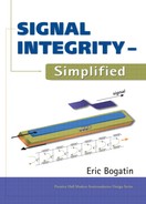
There is a new fundamental entity, called magnetic-field line loops, which surrounds every current. If we have a straight wire, as shown in Figure 6-1 for example, and send a current of one Amp through it, there will be concentric circular magnetic-field line loops created around the wire. These loops exist up and down the length of the wire. Imagine walking along the wire and counting the specific number of field line loops that completely surround it; the farther from the surface of the current, the fewer the number of field line loops will be encountered. If we move far enough away from the surface, we will count very few magnetic-field line loops.
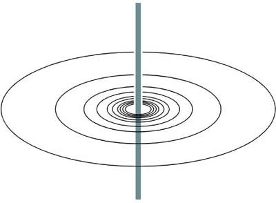
Figure 6-1. Some of the circular magnetic-field line loops around a current. The loops exist up and down the length of the wire.
These field line loops have a specific direction, as though they are circulating around the wire. To determine their direction, use the familiar right-hand rule: point the thumb of your right hand in the direction of the positive current and your fingers in the direction the field line loops circulate. This is illustrated in Figure 6-2.
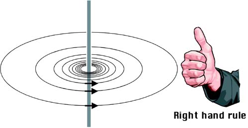
Figure 6-2. The direction of circulation of the magnetic-field line loops is based on the right-hand rule.
TIP
Magnetic-field line loops are always complete circles and always enclose some current. There must be some current encircled by the field line loops.
In what units do we count the field line loops? We count pens in units of gross. There are 144 pens in a gross. Paper in units of reams is counted, with 500 pages to each ream. Apples are counted by the bushel, which is a volume measure rather than a specific unit measure of apples. So how many apples are there in a bushel? The number is influenced by the shape and size of the apples. It's not clear exactly how many apples in a bushel, but there is some number.
Likewise, we count the number of magnetic-field line loops around a current in units of Webers. Like the apples in a bushel, the number of magnetic-field line loops in a Weber of field line loops is influenced by a number of factors.
What influences the number of field line loops around a current? There are a lot of factors. First is the amount of current in the conductor. If we double the current in the wire, we will double the number of Webers of magnetic-field line loops that are around it.
Second, the length of the wire around which the field line loops appear will affect the number of field line loops we count. The longer the wire length, the more field line loops there will be. Third, the cross section of the wire affects the total number of field line loops surrounding the current. This is a second-order effect and is more subtle. As we shall see, if the cross-sectional area is increased, for example if the wire is made thicker, the number of field line loops will decrease a little bit.
Fourth, the presence of other currents nearby will affect the number of field line loops around the first current. A special current to watch for is the return current. As the return current is brought closer, some of its field line loops will be around the first current and will change the total number of field line loops. On the other hand, the presence of dielectric materials does not affect the number of field line loops around the current.
TIP
Magnetic fields do not interact with dielectric materials at all. There is no change in the number of magnetic-field line loops around a current if it is surrounded with Teflon or with barium titanate.
Fifth, the metal of which the wire is composed will affect the total number of magnetic-field lines around the current only if the conductor contains iron, nickel, or cobalt. These three metals are called the ferromagnetic metals. They, or alloys containing them, have a permeability greater than 1. If any magnetic-field line loops are completely contained within one of these metals, the metal will have the effect of dramatically increasing the number of field line loops. However, it is only those field line loops that are circulating internally in the conductor that will be affected. Two common interconnect alloys, Alloy 42 and Kovar, are ferromagnetic because they both contain iron, nickel, and cobalt.
The composition of a wire made of any other metal, such as copper, silver, tin, aluminum, gold, lead, or even carbon, will have absolutely no effect on the number of field line loops around the current.
Inductance is fundamentally related to the number of magnetic-field line loops around a conductor, per amp of current through it.
TIP
Inductance is about the number of loops of magnetic-field lines enclosing a current, not about the absolute value of the magnetic field at any one point. Don't worry about magnetic-field concentration, worry about the number of magnetic-field line loops.
The units we use to measure inductance are Webers of field line loops per Amp of current. One Weber/Amp is given the special name, Henry. The inductance of most interconnect structures is typically such a small fraction of a Henry, it is more common to use the units of nanoHenry. A nanoHenry, abbreviated as nH, is a measure of how many Webers of field line loops we would count around a conductor per Amp of current through it:
where:
L = the inductance, in Henrys
N = the number of magnetic-field line loops around the conductor, in Webers
I = the current through the conductor, in Amps
If the current through a conductor doubles, the number of field line loops doubles but the ratio stays the same. This ratio is completely independent of how much current is going through the conductor. A conductor has the same inductance if 0 Amps are flowing through it or 100 Amps. Yes, the number of field line loops changes, but the ratio doesn't, and inductance is the ratio.
TIP
This means that inductance is really related to the geometry of the conductors. The only thing that influences inductance is the distribution of the conductors and in the case of ferromagnetic metals, their permeability.
We can apply this simple definition to all cases involving inductance. What makes it complicated and confusing is having to keep track of how much of the current loop we are counting the field line loops around and which other currents are present, creating field line loops. This gives rise to many qualifiers for inductance.
To keep track of the source of the magnetic-field line loops, we will use terms of self-inductance and mutual inductance. To keep track of how much of the current loop around which we are counting field line loops, we will use terms loop inductance and partial inductance. Finally, when referring to the magnetic-field line loops around just a section of an interconnect, while the current is flowing in the entire loop, we will use the terms total inductance, net inductance, or effective inductance.
Just using the term inductance is very ambiguous. We must develop the discipline to always use the qualifier of the exact type of inductance to which we are referring. The most common source of confusion arises from mixing up the various types of inductance.
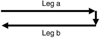
If the only current that existed in the universe were the current in a single wire, the number of field line loops around it would be easy to count. However, when there are other currents nearby, their magnetic-field line loops can encircle many different currents. Consider two adjacent wires, labeled a and b, as shown in Figure 6-3. If there were current in only one wire, a, it would have some number of field line loops around it and some inductance.
Figure 6-3. Magnetic-field line loops around one conductor can arise from its own currents and from another current.
Suppose there were to be some current in the second wire, b. It would have some field line loops around it, and hence, it would have some inductance. And, some of the field line loops from this wire, b, would also encircle the first wire, a. Around the first wire, a, there are now some field line loops from its own current and some field line loops from the adjacent, second current, b.
When we count field line loops around one wire, we need a way of keeping track of the source of the field line loops. We do this by labeling those field line loops from a wire's own currents as the self-field line loops and those from an adjacent current's, the mutual-field line loops.
TIP
The self-field line loops are those field line loops around a wire that arise from its own currents only. The mutual-field line loops are those magnetic-field line loops completely surrounding a wire that arise from another wire's current.
Every field line that is from wire b and goes around wire a must also be around both of them. In this way, we say the mutual-field line loops “link” the two conductors.
If we have two adjacent wires and we put current in the second wire, it will have some of its field line loops around the first wire. As we might imagine, if we move the second wire farther away, the number of mutual-field line loops that are around both wires will decrease. Move them closer and the number of mutual-field line loops will increase.
But, what happens to the total number of field line loops around the first wire? If there is current through both wires, they will each have some self-field line loops. If the currents are in the same direction, the circulation direction of their self-field line loops will be the same. To count the total number of field line loops around the first wire, we would count its self-field line loops plus the mutual-field line loops from the second wire, because they are both circulating in the same direction.
However, if the direction of their currents is opposite, the circulation direction of the self- and mutual-field line loops around the first wire will be opposite. The mutual-field line loops will subtract from the self-field line loops. The total number of field line loops around the first wire will be decreased due to the presence of the adjacent opposite current.
Given this new perspective of keeping track of the source of the field line loops, we can make inductance more specific.
TIP
We use the term self-inductance to refer to the number of field line loops around a wire per Amp of current in its own wire. What we normally think of as inductance we now see is really specifically the self-inductance of a wire.
The self-inductance of a wire will be independent of the presence of another conductor's current. If we bring a second current near the first wire, the total number of field line loops around the first may change, but the number of field line loops from its own currents will not.
TIP
Likewise, we use the term mutual inductance to refer to the number of field line loops around one wire per Amp of current in another wire.
As we bring the two wires close together, their mutual inductance increases. Pull them farther apart and their mutual inductance decreases. Of course, the units we use to measure mutual inductance are also nH, since it is the ratio of a number of field line loops per amp of current.
Mutual inductance has two very unusual and subtle properties. Mutual inductance is symmetric. Whether we send one Amp of current in one wire and count the number of field line loops around the other wire, or send one Amp of current through the other and count the field line loops it produces around the first, we get exactly the same ratio of field line loops per Amp of current. In this respect, mutual inductance is related to the field line loops that link two conductors and is tied to both of them equally. We sometimes refer to the “mutual inductance between two conductors,” because it is a property shared equally by the two conductors.
This is true no matter what the size or shape of each individual wire. One can be a narrow strip and the other a wide plane. The number of field line loops around one conductor per Amp of current in the other conductor is the same whether we send the current in the wide conductor or the narrow one.
The second property is that the mutual inductance between any two conductors can never be greater than the self-inductance of either one. After all, every mutual-field line loop is coming from one conductor and must also be a self-field line loop of that conductor. Since the mutual inductance between two conductors is independent of which one has the source current, it must always be less than the smallest of the two conductors' self-inductance.
A special property of magnetic-field line loops is that when the actual, total number of field line loops around a section of a wire changes, for whatever reason, there will be a voltage created across the length of the conductor. This is illustrated in Figure 6-4. The voltage created is directly related to how fast the total number of field line loops changes:
where:
V = the voltage induced across the ends of a conductor
ΔN = the number of field line loops that change
Δt = the time in which they change
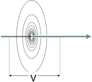
Figure 6-4. Voltage induced across a conductor due to the changing number of magnetic-field line loops around it.
If the current in a wire changes, the number of self-field line loops around it will change and there will be a voltage generated across the ends of the wire. The number of field line loops around the wire is N = L × I, where L in this example is the self-inductance of the section of the wire. The voltage created, or induced, across a wire can be related to the inductance of the wire and how fast the current in it changes:
TIP
Induced voltage is the fundamental reason why inductance plays such an important role in signal integrity. If there were no induced voltage when a current changed, there would be no impact from inductance on a signal. This induced voltage from a changing current gives rise to transmission line effects, discontinues, cross talk, switching noise, rail collapse, ground bounce, and most sources of EMI.
This relationship is, after all, the definition of an inductor. If we change the current through an inductor, we get a voltage generated across it. This voltage polarity is created to drive an induced current that would counteract the change in current. This is why we say, “an inductor resists a change in current.”
If we happened to have an adjacent current in another wire, near the first wire, some of the field line loops from this second wire may also surround the first wire. If the current in the second wire changes, the number of its field line loops around the first wire will change. This changing number of field line loops will cause a voltage to be created across the first wire. This is illustrated in Figure 6-5. These changes in the mutual-field line loops contribute to the induced voltage across the first wire. When it is another conductor in which the current changes, we typically use the term cross talk to describe the induced noise in the adjacent conductor. In this case, the voltage noise generated is:
where:
Vnoise = the voltage noise induced in the first, quiet wire
M = the mutual inductance between the two wires
I = the current in the second wire
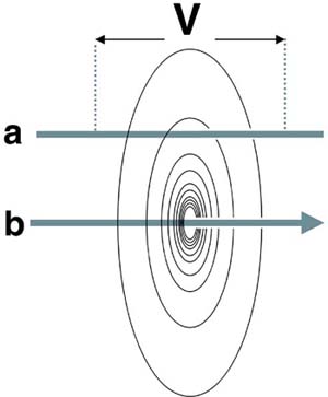
Figure 6-5. Induced voltage on one conductor due to a changing current in another and the subsequent changing mutual field lines between them are a form of cross talk.
Because the voltage induced depends on how fast the current changes, we sometimes use the term switching noise or delta I noise when describing the noise created when the current switches through an inductance.
To be able to analyze real-world problems that involve multiple conductors, we need to be able to keep track of all the various currents that are the sources of field line loops. The effects are the same; it's just more complicated when there are many conductors, each with possible currents and magnetic-field line loops.
Of course, real currents only flow in complete circuit loops. In the previous examples, we have been looking at just a section of a wire, where the only current that exists is the specific current in the section of wire we had drawn. As we have been counting field line loops, we have assumed that there was no current in the rest of the current loop to which this wire segment belonged. This type of inductance is called the partial inductance of the wire, accounting for the fact that we are looking at only a part of the current loop and assuming there are no other currents in the rest of the loop.
It is important to keep in mind that when we speak of partial inductance, the rest of the loop does not exist. It is not that we are ignoring it; it is that, in the view of partial inductance, there are no other currents that exist, except in the specific section of the conductor in which we are looking. The concept of partial inductance is a mathematical construct. It can never be measured, since an isolated current can never exist.
TIP
In reality, we can never have a partial current—we must always have current loops. However, the concept of partial inductance is a very powerful tool to understand and calculate the other flavors of inductance, especially if we don't know what the rest of the loop looks like yet.
Partial inductance has two flavors; partial self-inductance and partial mutual inductance. What we have been discussing above has really been the partial inductance of sections of two wires. More often than not, when referring to the inductance of a lead in a package, or a connector pin, or a surface trace, we are really referring to the partial self-inductance of this interconnect element.
The precise definition of partial self- and mutual inductance is based on a mathematical calculation of the number of field line loops around a section of a wire. Take a fixed-length section of conductor that might be part of a current loop. Rip it out of the loop so it is isolated in space but maintains its original geometry. On the ends, put large planes that are perpendicular to the length of the conductor. Now imagine injecting 1 A of current, appearing suddenly in one end of the wire, traveling through the wire, coming out the other end, and disappearing back into nothing when it exits.
The only current that exists in the universe is in the section of wire between the end planes. From this small section of current, count the number of field line loops that fit between the two end-cap planes. The number of field line loops counted, per the 1A of current in the wire section, is the partial self-inductance of that section of the conductor. Obviously, if we make the section of the wire longer, the total number of field line loops surrounding it will increase and the partial self-inductance will increase.
Now bring another short section of interconnect near this first section. Inject current from nowhere into the second wire and have it disappear out the opposite end. This partial current will create magnetic-field line loops throughout space, some of which will fit within the plane end caps of the first partial section of wire, completely enclosing the first wire segment. The number of field line loops around the first conductor segment, per amp of current in the second wire, is the partial mutual inductance between the two sections.
Obviously, in the real world, we can't create a current into the end of the wire without it coming from some other part of a circuit. However, we can perform this operation mathematically. This term, partial inductance, is a very well-defined quantity, it just can't be measured. As we shall see, it is a very powerful concept to facilitate optimizing the design for reduced ground bounce and calculating the other, measurable terms of inductance.
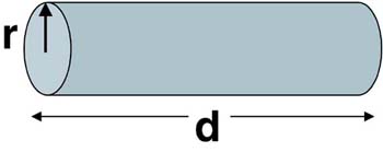
There are only a few geometries of conductors with a reasonably good approximation for their partial self-inductance. The partial self-inductance of a straight, round conductor, illustrated in Figure 6-6, can be calculated to better than a few percent accuracy using a simple approximation. It is given by:
where:
L = partial self-inductance of the wire, in nH
r = radius of the wire, in inches
d = length of the wire in inches
For example, an engineering change wire is typically 30-gage wire, or roughly 10 mils in diameter. For a length that is one inch long, the partial self-inductance is:
TIP
This gives rise to an important rule of thumb: the partial self-inductance of a wire is about 25 nH/inch or 1 nH/mm. Always keep in mind, this is a rule of thumb and sacrifices accuracy for ease of use.
We see that the partial self-inductance increases as we increase the length of the conductor. But, surprisingly, it increases faster than just linearly. If we double the length of the conductor, the partial self-inductance increases by more than a factor of two. This is because as we increase the length of the wire, there are more field line loops around this newly created section of the wire from the current in the new section, and some field line loops from the current in the other part of the wire are also around this new section.
The partial self-inductance decreases as the cross-sectional area increases. If we make the radius of the wire larger, the current will spread out more and the partial self-inductance will decrease. As we spread out the current distribution, the total number of field line loops will decrease.
TIP
This points out a very important property of partial self-inductance: the more spread out the current distribution, the lower the partial self-inductance. The more dense we bring the current distribution, the higher the partial self-inductance.
In this geometry of a round rod, the partial self-inductance varies only with the natural log of the radius, so it is only weakly dependent on the cross-sectional area. Other cross sections, such as wide planes, will have a partial self-inductance that are more sensitive to spreading out the current distribution.
Using the rule of thumb above, we can estimate the partial self-inductance of a number of interconnects. A surface trace from a capacitor to a via, 50 mils long, has a partial self-inductance of about 25 nH/inch × 0.05 inch = 1.2 nH. A via through a board, 064 mils thick, has a partial self-inductance of about 25 nH/inch × 0.064 inch = 1.6 nH.
Both the approximation and the rule of thumb are very good estimates of the partial self-inductance of a narrow rod. Figure 6-7 compares the estimated partial self-inductance for a 1-mil-diameter wire bond, based on the rule of thumb and the approximation given above, with the calculation from a 3D field solver. For lengths of typical wire bonds, about 100 mils long, the agreement is very good.
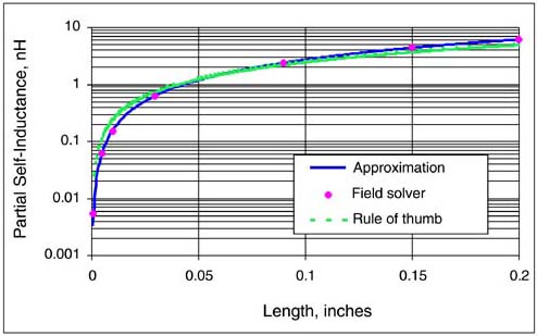
Figure 6-7. Partial self-inductance of a round rod, 1 mil in diameter, comparing the rule of thumb, the approximation, and the results from the Ansoft Q3D field solver.
The partial mutual inductance between two conductor segments is the number of field line loops from one conductor that completely surround the other conductor's segment. In general, the partial mutual inductance between two wires is a small fraction of the partial self-inductance of either one and drops off very rapidly as the wires are pulled apart. The partial mutual inductance between two straight, round wires can be approximated by:
where:
M = partial mutual inductance, in nH
d = length of the two rods, in inches
s = center-to-center separation, in inches
This formidable approximation takes into account second-order effects and is often referred to as a second-order model. It can be simplified by a further approximation when the separation is small compared to the length of the rods (s << d) as:
This is a first-order model, as it ignores some of the details of the long-range coupling between the rods. What it sacrifices in accuracy is made up for in being slightly easier to use. Figure 6-8 shows the predictions for the mutual inductance between two rods, as the rods are moved farther apart, and how they compare with the predictions from a 3D field solver. We see that when the partial mutual inductance is greater than about 20% of the partial self-inductance (i.e., when mutual inductance is significant), the first-order approximation is pretty good. It is a good, practical approximation.
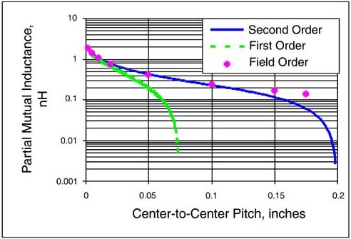
Figure 6-8. Partial mutual inductance between two round rods, 0.1 inch long, as their center-to-center separation increases, comparing the accurate approximation, the simplified approximation, and the result from Ansoft's Q3D field solver.
For example, two wire bonds may each have a partial self-inductance of 2.5 nH, if they are 100 mils long. If they are on a 5-mil pitch, they will have a partial mutual inductance of 1.3 nH. This means that if there were 1A of current in one wire bond, there would be 1.3 nH × 1 Amp = 1.3 nanoWebers of field line loops around the second wire bond. The ratio of the partial mutual inductance between the two wire bonds to the partial self-inductance of either one is about 50% with this separation.
TIP
From the graph of the mutual inductance and spacing, a good rule of thumb can be identified: if the spacing between two conductor segments is farther apart than their length, their mutual inductance is less than 10% of the partial self-inductance of either one and can often be ignored.
This says, the coupling between two sections of an interconnect are not important if they are farther apart than their length. For example, two vias 20 mils long have virtually no coupling between them if they are spaced more than 20 mils apart, center to center.
The concept of partial inductance is really the fundamental basis for all aspects of inductance. All the other forms of inductance can be described in terms of partial inductance. Package and connector models are really based on partial inductances. The output result of 3D static field solvers, when they calculate inductance values, is really in partial-inductance terms. SPICE models really use partial-inductance terms.
Consider a wire that is straight for some length and then loops back on itself, as shown in Figure 6-9, making a complete loop. This sort of configuration is very common for all interconnects, including signal and return paths and power paths and their ground-return paths. For example, it is common to have adjacent power-and ground-return wire bonds in a package. The pair could be adjacent signal and return leads in an IC package, or they could be an adjacent signal and a return plane pair in a circuit board.
When current flows in the loop, magnetic-field line loops are created from each of the two legs. If the current in the loop changes, the number of field line loops around each half of the wire would change. Likewise, there would be a voltage created across each leg that would depend on how fast the total number of field line loops around each leg was changing.
The voltage noise created across one leg of the current loop depends on how fast the total number of field line loops around the leg changes, while it is part of this complete current loop. The total number of field line loops around one leg arises from the current in that leg (the partial self-field line loops) and the field line loops coming from the other leg (the partial mutual-field line loops). But, the field line loops from the two currents circulate around the leg in opposite directions, so the total number of field line loops around this section of the loop is the difference between the self- and mutual-field line loops around it. The total number of field line loops per amp of current around this leg is given the special name effective inductance, total inductance, or net inductance.
TIP
Effective, net, or total inductance of a section of a loop is the total number of field line loops around just this section, per amp of current in the loop. This includes the contribution of field line loops from all the current segments in the complete loop.
We can calculate the effective inductance of one leg, based on the partial inductances of the two legs. Each of the two legs of the loop has a partial self-inductance associated with it, which we label as La and Lb. There is a partial mutual inductance between the two legs, which we label as Lab. We label the current in the loop, I, which is the same current in each leg, but of course, going in opposite directions.
If we could distinguish the separate sources of the field line loops around leg b, we would see some of the field line loops come from the current in leg b and are self-field lines. Around leg b, there would be Nb = I × Lb field line loops from its own current. At the same time, some of the field line loops around leg b are mutual field line loops and come from the current in leg a. The number of mutual field line loops coming from leg a, surrounding leg b is Nab = Lab × I.
What is the total number of field line loops around leg b? Since the current in leg a is moving in the opposite direction as leg b, the field line loops from leg a, around leg b, will be in the opposite direction as the field line loops from the current in leg b. When we count the total number of field line loops around leg b, we will be subtracting both sets of field line loops. The total number of field line loops around leg b is:
We call (Lb – Lab) the total, net, or effective inductance of leg b. It is the total number of field line loops around leg b, per amp of current in the loop, including the effects of all the current segments in the entire loop. When the adjacent current is in the opposite direction, as when the two legs are part of the same loop and one leg has the return current for the other leg, the effective inductance will determine how much voltage is created across one leg when the current in the loop changes. When the second leg is the return path, we call this voltage generated across the return path ground bounce.
The ground-bounce voltage drop across the return path is:
where:
Vgb = the ground-bounce voltage
Ltotal = the total inductance of just the return path
I = the current in the loop
Lb = the partial self-inductance of the return-path leg
Lab = the partial mutual inductance between the return path and the initial path
If the goal is to minimize the voltage drop in the return path (i.e., the ground-bounce voltage), there are only two approaches. First, we can do everything possible to decrease the current change in the loop. This means slow down the edges and limit the number of signal paths that use the same, shared return path. Rarely do we have the luxury of affecting these terms much. However, we should always ask.
Secondly, we must find every way possible to decrease Ltotal. There are only two knobs to tweak to decrease the total inductance of the return path: decrease the partial self-inductance of the leg and increase the partial mutual inductance between the two legs. Decreasing the partial self-inductance of the leg means making the return path as short and wide as possible (i.e., use planes). Increasing the mutual inductance between the return path and the initial path means doing everything possible to bring the first leg and its return path as close together as possible.
TIP
Ground bounce is the voltage between two points in the return path due to a changing current in a loop. Ground bounce is the primary cause of switching noise and EMI. It is primarily related to the total inductance of the return path. To decrease ground-bounce voltage noise, there are two significant features to change: decrease the partial self-inductance of the return path by using short lengths and wide interconnects, and increase the mutual inductance of the two legs by bringing the current and its return path closer together.
Surprisingly, decreasing ground bounce on the return path requires more than just doing something to the return path. It also requires thought about the placement of the initial current path and the resulting partial mutual inductance with the return path.
We can evaluate how much the net inductance of one wire bond can be reduced by bringing an adjacent wire bond closer, using the approximations above. Suppose one wire bond carries the power current and the other carries the ground-return current. They would have equal and opposite currents. In this case, the partial mutual inductance between them will act to decrease the total inductance of one of them: Ltotal = La – Lab. The closer we bring the wires, the greater the partial mutual inductance between them and the greater the reduction in the total inductance of one of the wires.
If each wire bond were 1 mil in diameter and 100 mils in length, the partial self-inductance of each would be about 2.5 nH. Using the approximation above for the partial self-inductance and the partial mutual inductance, we can estimate the net or effective inductance of one wire bond as we change the center-to-center spacing, s.
When the spacing is greater than 100 mils, the partial mutual inductance is less than 10% of the partial self-inductance. The effective inductance of one wire bond is nearly the same as its isolated partial self-inductance. But, when we bring them as close as 5 mils center-to-center pitch, the mutual inductance increases considerably and we can reduce the effective inductance of one wire bond down to 1.3 nH. This is a reduction of more than 50%. The lower the effective inductance, the lower the voltage drop across this wire bond and the less ground-bounce voltage noise the chip will experience.
If the effective inductance of one wire bond, when the other current is far away, is 2.5 nH and there is 100 mA of current that switches in 1 nsec (typical of what goes into a transmission line), the ground-bounce voltage generated across the wire bond is Vgb = 2.5 nH × 0.1A/1 nsec = 250 mV. This is a lot of voltage noise. When the two wire bonds are routed close together, with a center pitch of 5 mils, the ground-bounce noise is reduced to Vgb = 1.3 nH × 0.1A/1 nsec = 130 mV—considerably less.
TIP
This demonstrates the very important design rule: to decrease effective inductance, bring the return current as close as possible to the other current.
Suppose we have the opposite case. Suppose that both wires will be carrying power current. This is often the case in many IC packages, because multiple leads are used to carry power and carry the ground return. If we look at the net inductance of one of the power wires and bring an adjacent power wire nearby, what happens?
In this case, both currents are in the same direction. The mutual-field line loops will be in the same direction as the self-field line loops. The mutual-field line loops from the second wire will add its field line loops to the field line loops already around the first wire. The net inductance of one of the power wires will be Ltotal = La + Lab.
If the goal is to minimize the net inductance of the power lead, our design goal, as always, is to do everything possible to decrease the partial self-inductance of the lead. However, in this case, because the field line loops from the adjacent wire are in the same direction, we must do everything possible to decrease their mutual inductance. This means space the wires out as much as possible.
We can estimate the net or effective inductance of one wire bond when the adjacent one carries the same current, for the two cases of current in the same direction or in opposite directions, as we pull them farther apart. This is plotted in Figure 6-10.

Figure 6-10. Total inductance of one 100-mil-long wire bond when an adjacent wire bond carries the same current, for the two cases of the currents in the same direction and in opposite directions. The wires are pulled apart, comparing the total inductances with the partial self- and mutual inductances.
As long as the two wires are farther apart than their length, the net inductance is not much different from the partial self-inductance of one. As they are brought closer together, the net inductance decreases when the currents are in opposite directions, but increases when the currents are in the same direction.
TIP
A good general design rule to minimize the net inductance of either leg in the power-distribution system is to keep similar parallel currents as far apart as their lengths.
In other words, if there are two adjacent wire bonds, each 100 mils long and both carrying power, they should be at least 100 mils center-to-center. Any closer and their mutual inductance will increase the effective inductance of each leg and increase the switching noise on one of the wires. This is not to say that there is no benefit for parallel currents in close proximity. It's just that their effectiveness is reduced over the maximum possible gain.
A common practice in high-power chips is double bonding, that is, using two wire bonds between the same pad on the die and the same pad on the package. The series resistance between the two pads will be decreased because of the two wires in parallel, and the equivalent inductance of the two wire bonds will be reduced compared to that when using only one wire bond. The closer the wires, the higher the mutual inductance, and the larger the effective inductance. But, since there are two in parallel, the equivalent inductance is half the total inductance of either one.
When double bonding, the loops should be created to keep the wires as far apart as possible. If they are 50 mils long and can be kept 5 mils apart, the partial self-inductance of either wire bond would be about 1.25 nH and their partial mutual inductance would be about 0.5 nH. Their effective inductance would be 1.75 nH. With the two in parallel, their equivalent inductance would be 1/2 × 1.75 nH = 0.88 nH. This is reduced from the 1.25 nH expected with just one wire bond. Double bonding can, in fact, decrease the equivalent inductance between two pads.
As another example, consider the vias from a decoupling capacitor's pads to the power- and ground-return planes below, as illustrated in Figure 6-11. Suppose the distance to the plane below is 20 mils, and the vias are 10 mils in diameter. Is there any advantage in using multiple vias in parallel from each pad of the capacitor?
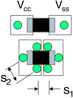
Figure 6-11. Via placement for decoupling capacitor pads between Vcc and Vss planes. Top: conventional placement. Bottom: optimized for low total inductance and lowest voltage-collapse noise: s2 > via length, s1 < via length.
If the center-to-center spacing, s, between the vias is greater than the length of a via, 20 mils, their partial mutual inductance will be very small and they will not interact. The net inductance of either one will be just its partial self-inductance. Having multiple vias in parallel from one pad to the plane below will reduce the equivalent inductance to the plane below inversely with the number of vias. The more vias there are in parallel, the lower the equivalent inductance. In the previous figure, this means s2 must be at least as large roughly as the distance to the planes, 20 mils. Likewise, if it is possible to bring vias with opposite currents closer together than their length, the effective inductance of each via will be reduced. If it is possible to place the vias with s1 less than 20 mils apart, the net inductance of each via will be reduced and the equivalent inductance from the pad to the plane below will be reduced and the rail-collapse voltage will be reduced.
TIP
This suggests the following design rule for minimizing the total inductance of either path: keep the center-to-center spacing between vias of the same current direction at least as far apart as the length of the via, keep the center-to-center spacing between vias with opposite direction current much closer than the length of the vias.
The general definition of inductance is the number of field line loops around a conductor per amp of current through it. In the real world, current always flows in complete loops. When we measure the total inductance of the complete current loop, we call it the loop inductance. This loop inductance is really the self-inductance of the entire current loop, or the loop self-inductance.
TIP
The loop self-inductance of a current loop is the total number of field line loops surrounding the entire loop, per amp of current in the loop. With 1 Amp in the loop, we start at one end of the loop, walk along the wire, and count the total number of field line loops we encounter from all the current in the loop. This includes the effect of the current distribution of each section of the wire.
Let's look at the loop self-inductance of the wire loop with two straight legs as in the example above. Leg a is like a signal path and leg b is like a return path. As we walk along leg a counting field line loops, we see the field line loops coming from the current in leg a (the partial self-inductance of leg a) and we see the field line loops around leg a coming from the current in leg b (or the partial mutual inductance between leg a and leg b).
Moving down leg a, the total number of field line loops we count is really the total inductance of leg a. When we move down leg b and count the total number of field line loops around leg b, we count the total inductance of leg b. The combination of these two is the loop self-inductance of the entire loop:
where:
Lloop = the loop self-inductance of the twin-lead loop
La = partial self-inductance of leg a
Lb = partial self-inductance of leg b
Lab = partial mutual inductance between legs a and b
This may look familiar, as it appears in many text books. What is often not explicitly stated and what often makes inductance confusing is that the self- and mutual inductances in this relationship are really the partial self- and mutual inductances.
This relationship says that as we bring the two legs closer together, the loop inductance will decrease. The partial self-inductances will stay the same; it is the partial mutual inductance that increases. In this case, the larger mutual inductance between the two legs will act to decrease the total number of field line loops around each leg and to reduce the loop self-inductance.
TIP
It is sometimes stated that the loop self-inductance depends on the “area of the loop.” While this is roughly true in general, it doesn't help feed our intuition much. As we have seen, it is not so much the area that is important, it is the total number of field line loops encircling each leg that is important.
For example, in Figure 6-12 we show two different current loops, each with exactly the same area. They will have different loop inductances, since the partial mutual inductances are so different. The closer together we bring the legs with opposite current, the larger their partial mutual inductances and the smaller the resulting loop inductance. As we have seen, the underlying mechanism for decreasing loop self-inductance is the increase in the partial mutual inductance between the signal and return paths when the return path is brought closer to the other leg and the loop is made smaller.
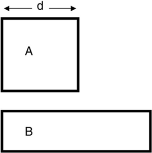
Figure 6-12. Two loops with exactly the same area but very different loop inductances. Bringing the return section of the loop closer to the other leg reduces the loop inductance by increasing the partial mutual inductance.
There are three important special-case geometries that have good approximations for loop inductance: a circular loop; two long, parallel rods; and two wide planes.
For a circular loop, the loop inductance is given by
where:
Lloop = loop inductance, in nH
R = radius of the loop, in inches
D = diameter of the wire making up the loop, in inches
For example, a 30-gauge wire, about 10 mils thick, that is bent in a circle with a 1-inch diameter, has a loop inductance of:
TIP
This is a good rule of thumb to remember. Hold your index finger and thumb in a circle. A loop of 30-gauge wire this size has a loop inductance of about 85 nH.
The loop inductance is not really proportional to the area or to the circumference. It is proportional to the radius times ln (radius). The larger the circumference, the larger the partial self-inductance of each section, but also, the farther away the opposite-direction currents in the loop and the lower their mutual inductance.
However, to first order, the loop inductance is roughly proportional to the radius. If the circumference is increased, the loop inductance will increase. For the 1-inch loop, the circumference is 1 inch × 3.14 or about 3.14 inches. This corresponds to a loop inductance per inch of circumference of 85 nH/3.14 inches ~ 25 nH/in. As a good rule of thumb, we see again that the loop inductance per length is about 25 nH/inch, for loops near 1 inch in diameter.
Figure 6-13 compares the loop inductance predicted by this approximation with the actual measured loop inductance of small copper wires. The accuracy is good to a few percent.
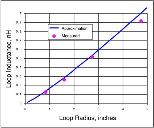
Figure 6-13. Comparison of the measured loop inductance of small loops made from 25-mil-thick wire with different loop radius and the predictions of the approximation. The approximation is seen to be good to a few percent.
The loop inductance of two adjacent, straight-round wires, assuming one carries the return current of the other, is given by:
where:
Lloop = loop inductance, in nH
len = the length of the rods, in inches
r = radius of the rods, in mils
s = center-to-center separation of the rods, in mils
For example, the loop inductance of two 1-mil-diameter wire bonds, 100 mils long and separated by 5 mils, is:
This relationship points out that the loop inductance of two parallel wires is directly proportional to the length of the wires. It scales directly with the natural log of the separation. Increase the separation and the loop inductance increases, but only slowly, as the natural log of the separation.
The loop inductance of long, straight, parallel rods is directly proportional to the length of the rods. For example, if the rods represent the conductors in a ribbon cable, with a radius of 10 mils and center-to-center spacing of 50 mils, the loop inductance for adjacent wires carrying equal and opposite current is about 16 nH for a 1-inch-long section.
In the special case when the signal and return paths have a constant cross section down their length, the loop inductance scales directly with the length, and we refer to the loop inductance per length of the interconnect. Signal and return paths in ribbon cable have a constant loop inductance per length. In the example above, the loop inductance per length of the ribbon-cable wires is about 16 nH/inch. In the case of two adjacent wire bonds, the loop inductance per length is 2.3 nH/0.1 inch, or 23 nH/inch.
As we shall see, any controlled-impedance interconnect will have a constant loop inductance per length.
When we think “signal integrity,” we usually think about reflection problems and cross talk between signal nets. Though these are important problems, they represent only some of the signal-integrity problems. Another set of problems is due not to the signal paths, but to the power and ground paths. We call this the power-distribution system or PDS. Planes play a crucial role in distributing the power- and ground-return currents primarily because of their potentially very low loop inductance.
The purpose of the PDS is to deliver a constant voltage across the power and ground pads of each chip. Depending on the device technology, this voltage difference is typically 5 v or 3.3 v or 2.4 v. Most noise budgets will allocate no more than 5% ripple on top of this. Isn't the regulator supposed to keep the voltage constant? If ripple is too high, why not just use a heftier regulator?
The expression “there's many a slip twixt cup and lip” pretty much summarizes the problem. Between the regulator and the chip are a lot of interconnects in the PDS—vias, planes, package leads, and wire bonds, for example. When current going to the chip changes (e.g., when the microcode causes more or fewer gates to switch, or at clock edges, where most gates tend to switch), the changing current, passing through the impedance of the PDS interconnects, will cause a voltage drop, called either rail droop or rail collapse.
To minimize this voltage drop from the changing current, the design goal is to keep the impedance of the PDS below a target value. There will still be changing current, but if the impedance can be kept low enough, the voltage drop across this impedance can be kept below the 5% allowed ripple.
TIP
The impedance of the PDS is kept low by two design features: the addition of low-impedance decoupling capacitors to keep the impedance low at lower frequencies and the minimization of the loop inductance between the decoupling capacitors and the chip's pads to keep the impedance low at higher frequencies.
How much decoupling capacitance is really needed? We can estimate roughly how much total capacitance is needed by assuming the decoupling capacitor provides all the charge that must flow for some time period, Δt.
During this time, the voltage across the capacitor, C, will drop as its charge is depleted by ΔQ, which has flowed through the chip. The voltage drop, ΔV, is given by:
where:
ΔV = the change in voltage across the capacitor
ΔQ = the charge depletion from the capacitor
C = the capacitance
How much current, I, flows through the chip? Obviously this depends strongly on the specific chip and will change a lot depending on the code running through it. However, we can get a rough estimate by assuming the power dissipation of the chip, P, is related to the voltage, V, across it, and the average current, I, through it. Given the chip's average power dissipation, the average current through the chip is:
The total amount of decoupling needed for the chip to be able to decouple for a time, Δt, is related by:
From this relationship, the time a capacitor will decouple can be found as:
or the capacitance required to decouple for a given time can be found from:
where:
Δt = the time during which the charge flows from the capacitor, in sec
0.05 = the 5% voltage droop allowed
C = the capacitance of the decoupling capacitor, in Farads
V = the voltage of the rail, in Volts
P = the power dissipation of the chip, in watts
For example, if the chip power is 1 watt, typical for a memory chip or small ASIC running at 3.3 v and with a 5% ripple allowed, the amount of total decoupling capacitance needed is about:
If the regulator cannot respond to a voltage change in less time than 10 microseconds, for example, then we need to provide at least 2 × 10 microsec = 20 microFarad capacitance for decoupling. Less than this and the voltage droop across the capacitor will exceed the 5% allowed ripple.
Why not just use a single 20-microFarad capacitor to provide all the decoupling required? The impedance of an ideal capacitor will decrease with increasing frequency. At first glance, it would seem that if a capacitor has low enough impedance (e.g., in the 1-MHz range) that the regulator cannot respond, then it should have even lower impedance at higher frequency.
Unfortunately, in real capacitors, there is a loop associated with the connection between the terminals of the capacitor and the rest of the connections to the pads on the chip. This loop inductance, in series with the ideal capacitance of the component, causes the impedance of a real capacitor to increase with increasing frequency.
Figure 6-14 is a plot of the measured impedance of an 0603 decoupling capacitor. This is the measured loop impedance between one end of the capacitor and the other, through a plane below the component. At low frequency, the impedance decreases, exactly as it does in an ideal capacitor. However, as the frequency increases, we reach a point where the series loop inductance of the capacitor begins to dominate the impedance. Above this frequency, called the self-resonant frequency, the impedance begins to increase. Above the self-resonant frequency, the impedance of the capacitor is completely independent of its capacitance. It is only related to its associated loop inductance. If we want to decrease the impedance of decoupling capacitors at the higher frequency end, we need to decrease their associated loop inductance, not increase the capacitance.
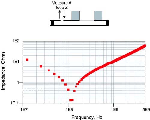
Figure 6-14. Measured loop impedance of a 1 nF 0603 decoupling capacitor, with a current loop configured as shown, measured with a Giga-Test Labs Probe Station.
TIP
A key feature of decoupling capacitors is that at high frequency, the impedance is solely related to their loop inductance, referred to as the equivalent series inductance (ESL). Decreasing the impedance of a decoupling capacitor at high frequency is all about decreasing the loop inductance of the complete path from the chip's pads to the decoupling capacitor.
The measured loop impedance of six 0603 decoupling capacitors with different values is shown in Figure 6-15. Their impedance at low frequency is radically different, since they have orders-of-magnitude different capacitance. However, at high frequency, their impedances are identical because they have the same mounting geometry on the test board.
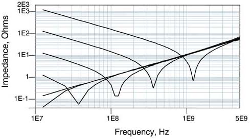
Figure 6-15. Measured loop impedance of 6 different 0603 capacitors with capacitances varying from 10 pF to 1 µF, but all with the same mounting geometry, measured with GigaTest Labs Probe Station.
TIP
The only way of decreasing the impedance of a decoupling capacitor at high frequency is by decreasing its loop self-inductance.
The best ways of decreasing the loop inductance of a decoupling capacitor are as follows:
Keep vias short by assigning the power and ground planes close to the surface.
Use small-body-size capacitors.
Use very short connections between the capacitor pads and the vias to the underlying planes.
Use multiple capacitors in parallel.
If the loop inductance associated with one decoupling capacitor and its mounting is 2 nH and the maximum allowed inductance is 0.1 nH, then there must be at least 20 capacitors in parallel for the equivalent loop inductance to meet the requirement.
From the decoupling capacitors to the chips' pads, the interconnect should be designed for the lowest loop inductance. In addition to short surface pads and short vias, planes are the interconnect geometry with the lowest loop inductance.
The loop inductance for a current path going down one plane and back the other, as illustrated in Figure 6-16, depends on the partial self-inductance of each plane path and the partial mutual inductance between them. The wider the planes, the more spread out the current distribution, the lower the partial self-inductance of each plane and the lower the loop inductance. The longer the planes, the larger their partial self-inductance and the larger the loop inductance. The closer we bring the planes, the larger their mutual inductance and the lower the loop inductance.
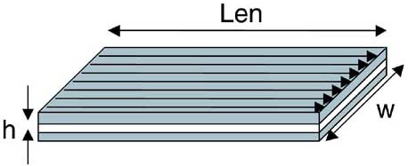
Figure 6-16. Geometrical configuration for the current flow in two planes forming a loop. The return current is in the opposite direction in the bottom plane.
For the case of wide conductors, where the width, w, is much larger than their spacing, h, or w >> h, the loop inductance between two planes is to a very good approximation given by:
where:
Lloop = the loop inductance, in nH
µ0 = permeability of free space = 32 nH/mil
h = spacing between the planes, in mils
Len = length of the planes, in mils
w = width of the planes, in mils
This assumes the current flows uniformly from one edge and back to the other edge.
If the section is in the shape of a square, the length equals the width, and the ratio is always 1, independent of the length of a side. It's startling that the loop inductance of a square section of a pair of planes that is 100 mils on a side is exactly the same as for a square section 1 inch on a side. Any square section of a pair of planes will have the same loop inductance. This is why we often use the term loop inductance per square of the planes, or the shortened version inductance per square of the board. It makes life more confusing, but now we know this really refers to the loop inductance between two edges of a square section of planes, when the other edges are shorted together.
For the thinnest dielectric spacing currently in volume production, 2 mils, our approximation above estimates the loop inductance per square as about Lloop = 32 pH/mil × 2 mil = 64 pH. As the dielectric thickness increases, the loop inductance per square increases. A dielectric spacing of 5 mils has a loop inductance per square of Lloop = 32 pH/mil × 5 mil = 160 pH.
As the spacing between adjacent planes increases, the partial mutual inductance will decrease and there won't be as many field line loops from one plane around the other to cancel out the total number of field line loops. With greater dielectric spacing, the loop inductance increases and the rail-collapse noise will increase. This will make the PDS noise worse and will also increase the ground-bounce noise that drives common-mode currents on external cables and causes EMI problems.
Current doesn't flow from one edge to another edge in planes. Between a discrete decoupling capacitor and the package leads, the connection to the planes is more like point contacts. In the above analysis we assumed the current was flowing uniformly down the plane. However, in actual practice, the current is not uniform. If the current is restricted due to point contacts, the loop inductance will increase.
The only reason we assumed the current was uniform was because this was the only case for which we had a simple approximation to help estimate the loop inductance. When balancing accuracy versus little effort to get an answer, we chose the path of little effort. The only way to get a better estimate of the loop inductance associated between two planes with real contacts is by using a 3D field solver.
We can gain some insight into how the geometry affects the associated loop inductance between two contact points between the planes. By using a 3D field solver, we can calculate the specific current distribution between the contact points and from the specific current distributions, the resulting loop inductance.
The good news about field solvers is that the accuracy can be very good, and they can include many real-world effects for which there are no good approximations. The bad news is that we can't generalize an answer from a field solver. It can run only one specific problem at a time.
As an example of the impact of the via contacts on the loop inductance between two planes, two special cases are compared. In both cases, a 1-inch-square section of two planes, 2 mils apart, was set up. In the first case, one edge of the top plane and the adjacent edge of the bottom plane were used as the current source and sink. The far ends of the planes were shorted together.
In the second case, two small via contacts were used as the current source and sink at one end and a similar pair of contacts shorted the planes together at the other end. The contacts were 10 mils in diameter, spaced on 25-mil centers, similar to how a pair of vias would contact the planes in an actual board.
Figure 6-17 shows the current distribution in one of the planes for each case. When the edge contact is used, the current distribution is uniform, as expected. The loop inductance between the two planes is extracted as 62 pH. The approximation above, for the same geometry, was 64 pH. We see that for this special case, the approximation is pretty good.
Figure 6-17. Current distribution in the top plane of a pair of planes with edge contact and a pair with point contacts. The lighter shade corresponds to higher current density. With edge contacts, the current distribution is uniform. With via point contacts, the current is crowded near the contact points. The higher current density creates higher inductance. Simulation with Ansoft's Q3D field solver, courtesy of Charles Grasso.
When the current flows from one via contact, down the board to a second via contact, through the via to the bottom plane, back through the board and up through the end vias, as would be the case in a real board, the loop inductance extracted by the field solver is 252 pH. This is an increase by about a factor of four. The increase in loop inductance between the planes is due to the higher current density where the current is restricted to flow up the via. The more constricted the current flow, the higher the partial self-inductance and loop inductance. This increase in loop inductance is sometimes referred to as spreading inductance. If the contact area were increased, the current density would decrease and the spreading inductance would decrease.
The loop inductance between the planes, even with the spreading inductance, will still scale with the plane-to-plane separation. Decrease the spacing and the spreading loop inductance will decrease.
TIP
From this example, we can develop a simple rule of thumb that for the case of 10-mil-diameter contacts, the plane-to-plane loop inductance is about four times the inductance per square in adjacent planes.
When many pairs of vias contribute current to the planes connecting many capacitors and many package leads, closely spaced planes will minimize the voltage drop from all the simultaneous dI/dt's.
The loop inductance, in the planes associated with the decoupling capacitor, is dominated by the spreading inductance, not by the distance between the chip and the capacitor. To a first order, the total loop inductance of the decoupling capacitor is only weakly dependent on its proximity to the chip. However, the closer the capacitor is to the chip, the more the high-frequency power and return currents will be confined to the proximity of the chip and the lower the ground-bounce voltage will be on the return plane.
TIP
By keeping decoupling capacitors close to the high-power chips, the high-frequency currents in the return plane can be localized to the chip and kept away from I/O regions of the board. This will minimize the ground-bounce voltage noise that might drive common currents on external cables and contribute to EMI.
A field solver is a useful tool to explore the impact of a field of via clearance holes on the loop inductance between two planes. Arrays of vias occur all the time. They happen under BGA packages, under connectors, and in very high-density regions of the board.
Often, there will be clearance holes in the power and ground planes of the via field. What impact will the holes have on the loop inductance of the planes? To a first order, we would expect the inductance to increase. But by how much? We often hear that an array of clearance holes under a package—the Swiss cheese effect—will dramatically increase the inductance of the planes. The only way to know by how much is to put in the numbers, that is, use a field solver.
Two identical pairs of planes were created, each 0.25 inch on a side and separated by 2 mils. Two via contacts were connected to each end of the planes. At one end, the vias were shorted together. At the other end, current was injected in one via and taken out from the other. This simulates one end connected to a decoupling capacitor and the other connected to the power and ground leads of a package through vias to the top surface.
In one pair of planes, a field of clearance holes was created in each plane. Each hole was 20 mils in diameter on 25-mil centers. This is an open area of about 50%. For each of the two cases, the current distribution was calculated and the loop inductance extracted with a 3D static field solver. Figure 6-18 shows the current distribution with and without the field of holes. The clearance holes constrict the current to the narrow channels between the holes, so we would expect to see the loop inductance increase.
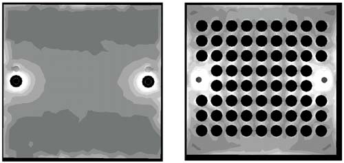
Figure 6-18. Current distribution on closely spaced planes with contact via points with and without a field of clearance holes. The lighter colors correspond to higher current densities. The holes cause the current to constrict, increasing the loop inductance. Simulated with Ansoft's Q3D field solver, courtesy of Charles Grasso.
The field solver calculates a loop inductance of 192 pH with no holes and 243 pH with this high density of holes. This is an increase of about 25% in loop inductance for an open area of 50%. We see that holes do increase the loop inductance of planes but not nearly as dramatically as we might have expected. To minimize the impact from the holes, it is important to make the holes as small as possible. Of course, bringing the planes closer together will also decrease the loop inductance of the planes, with or without clearance holes.
It is important to note that while a field of clearance holes in the power and ground planes will increase the loop inductance, the loop inductance can be kept well below a factor of two increase. It is not nearly as much of a disaster as commonly believed.
TIP
The optimum power and ground interconnects, for lowest loop inductance, are planes, as wide as possible and as closely spaced as possible. When we use a very thin dielectric between the planes, we reduce the loop inductance between the bulk decoupling capacitors and the chip's pads. This will decrease the rail collapse and EMI.
Both of these problems, rail collapse and EMI, will get worse as rise times decrease. As we move into the future of higher and higher clock frequencies, thin dielectrics in the power-distribution network will play an increasingly important role.
If there are two independent current loops, there will be a mutual inductance between them. The loop mutual inductance is the number of field line loops from the current in one loop that completely surrounds the current of the second loop, per amp of current in the first loop.
When current in one loop changes, it will change the number of field line loops around the second current loop and induce noise in the second current loop. The amount of noise created is:
where:
Vnoise = the voltage noise induced on one loop
Lm = the loop mutual inductance between the two loops
dI/dt = how fast the current in the second loop changes
The noise in the quiet loop will happen only when there is a dI/dt in the active loop, which is only during the switching transitions. This is why this sort of noise is often called switching noise, or simultaneous switching noise (SSN), or delta I noise.
TIP
The most important way of reducing switching noise is reducing the mutual inductance between the signal- and returnpath loops. This can be accomplished by moving the loops farther apart from each other. Since the mutual inductance between two loops can never be greater than the self-inductance of the smallest loop, another way of decreasing the loop mutual inductance is to decrease the loop self-inductance of both loops.
Loop mutual inductance also contributes to the cross talk between two uniform transmission lines and is discussed in a later chapter.
So far, we have been considering just the partial inductance associated with a single interconnect element that has two terminals, one on either end, and then the resulting loop inductance consisting of the two elements in series. For two separate interconnect elements, there are two ways of being connected together: end to end (in series) or with each end together (in parallel). These two circuit configurations are illustrated in Figure 6-19.
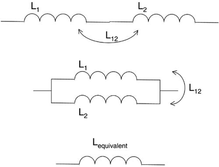
Figure 6-19. Circuit topologies for combining partial inductors in series (top) and in parallel (middle) into an equivalent inductance (bottom).
When connected together, the resulting combination has two terminals, and there is an equivalent inductance for the combination. We are used to thinking about the equivalent inductance of a series combination of two inductors simply as the sum of each individual partial self-inductance. But what about the impact from the mutual inductance?
The inclusion of the mutual inductance between the interconnect elements makes the equivalent inductance a bit more complicated. For the series combination of two partial inductances, the resulting equivalent partial self-inductance of the series combination is:
The equivalent partial self-inductance when the elements are connected in parallel is given by:
where:
Lseries = the equivalent partial self-inductance of the series combination
Lparallel = the equivalent partial self-inductance of the parallel combination
L1 = partial self-inductance of one element
L2 = partial self-inductance of the other element
L12 = the partial mutual inductance between the two elements
When the partial mutual inductance is zero, and the partial self-inductances are the same, both of these reduce to the familiar expressions of the series combination. That is, they are just twice the self-inductance of one of them and the equivalent parallel inductance is just half the partial self-inductance of one of them.
In the special case when the partial self-inductance of the two inductors is the same, the series combination of the two inductors is just twice the sum of the self- and mutual inductance. For the parallel combination, when the two partial self-inductances are equal, the equivalent inductance is:
where:
Lparallel = the equivalent partial self-inductance of the parallel combination
L = the partial self-inductance of either element
M = the partial mutual inductance of either element
This says that if the goal is to reduce the equivalent inductance of two current paths in parallel, we do get a reduction, as long as the mutual inductance between the elements is kept small.
All the various flavors of inductance are directly related to the number of magnetic-field line loops around a conductor per amp of current. The importance of inductance is due to the induced voltage across a conductor when currents change. Just referring to an inductance can be ambiguous.
To be unambiguous, we need to specify the source of the currents, as in the self-inductance or mutual inductance. Then we need to specify whether we are referring to part of the circuit using partial inductance or the whole circuit using loop inductance. When we look at the voltage noise generated across part of the circuit, because this depends on all the field line loops and how they change, we need to specify the total inductance of just that section of the circuit. Finally, if we have multiple inductors in some combination, such as multiple parallel leads in a package or vias in parallel, we need to use the equivalent inductance.
The greatest source of confusion arises when we misuse the term inductance. As long as we include the correct qualifier, we will never go wrong. The various flavors of inductance are listed here:
Inductance: the number of field line loops around a conductor per amp of current through it.
Self-inductance: the number of field line loops around the conductor per amp of current through the same conductor.
Mutual inductance: the number of field line loops around a conductor per amp of current through another conductor.
Loop inductance: the total number of field line loops around the complete current loop per amp of current.
Loop self-inductance: the total number of field line loops around the complete current loop per amp of current in the same loop.
Loop mutual inductance: the total number of field line loops around a complete current loop per amp of current in another loop.
Partial inductance: the number of field line loops around a section of a conductor when no other currents exist anywhere.
Partial self-inductance: the number of field line loops around a section of a conductor per amp of current in that section when no other currents exist anywhere.
Partial mutual inductance: the number of field line loops around a section of a conductor per amp of current in another section when no other currents exist anywhere.
Effective, net, or total inductance: the total number of field line loops around a section of a conductor per amp of current in the entire loop, taking into account the presence of field line loops from current in every part of the loop.
Equivalent inductance: the single self-inductance corresponding to the series or parallel combination of multiple inductors including the effect of their mutual inductance.
In evaluating the resistance and inductance of conductors, we have been assuming the currents were uniformly distributed through the conductors. While this is the case for DC currents, it is not always true when currents change. AC currents can have a radically different current distribution, which can dramatically affect the resistance and to some extent the inductance of conductors.
It is easiest to calculate the current distributions in the frequency domain where currents are sine waves. This is a situation where moving to the frequency domain gets us to an answer faster than staying in the time domain.
At DC frequency, the current distribution in a solid rod is uniform throughout the rod. When we counted magnetic-field line loops previously, we focused on the field line loops that were around the outside of the conductor. In fact, there are some magnetic-field line loops inside the conductor as well. They are also counted in the self-inductance. This is illustrated in Figure 6-20.
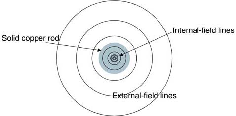
Figure 6-20. Magnetic-field line loops from the DC current in a uniform solid rod of copper. Some of the field line loops are internal- and some are external-field line loops.
To distinguish the magnetic-field line loops contributing to the conductor's self-inductance that are enclosed inside the conductor from those that are outside the conductor, we separate the self-inductance into internal self-inductance and external self-inductance.
The internal magnetic-field line loops are the only field line loops that actually see the conductor metal and can be affected by the metal. For a round wire, the external-field line loops never see any conductor and they will never change with frequency. However, the internal-field line loops do see the conductor and they can change as the current distribution inside the conductor changes with frequency.
Consider two cylinders of current with exactly the same cross-sectional area in a solid rod of copper, as shown in Figure 6-21. If the cross-sectional area of each is exactly the same, each cylinder has the same current. Which cylinder has more field line loops around it?
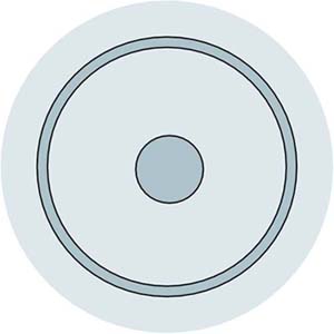
Figure 6-21. Two cylinders of current, traveling into the paper, singled out in a solid rod of copper, both of exactly the same cross-sectional area.
The outer cylinder and the inner cylinder have exactly the same number of field line loops in the region outside the outer cylinder. The number of field line loops outside a current is only related to the amount of total current enclosed by the field line loops. There are no field line loops from currents in the outer cylinder inside this cylinder, since field line loops must encircle a current.
The current from the inner cylinder has more internal self-field line loops, since it has more distance from its current to the outer wall of the rod. The closer to the center of the rod the current is located, the greater the total number of field line loops around that current.
TIP
Currents closer to the center of the rod will have more field line loops per amp of current and a higher self-inductance than currents toward the outside of the conductor.
Now, we turn on the AC current. Currents are sine waves. Each frequency component will travel the path of lowest impedance. The current paths that have the highest inductance will have the highest impedance. As the sine-wave frequency increases, the impedance of the higher inductance paths get even larger. The higher the frequency, the greater the tendency for current to want to take the lower inductance path. This is the path toward the outer surface of the rod.
In general, the higher the frequency, the greater the tendency for current to travel on the outside surface of the conductor. At a given frequency, there will be some distribution of current from the center to the outside surface. This will depend on the relative amount of resistive impedance and inductive impedance. The higher the current density the higher the voltage drop from the resistive impedance. But the higher the frequency, the bigger the difference between the inductive impedance of the inner and outer paths. This balance means the current distribution changes with frequency, tending toward all the current in a thin layer around the outer surface, at high frequency.
TIP
As the frequency of the sine waves of current through the rod increases, the current will redistribute so most of the current is taking the path of lowest impedance, that is, toward the outside of the conductor. At high frequency, it appears as though all the current is traveling in a thin shell at the conductor's surface.
There are only a few simple geometries where there is a good approximation for the actual current distribution of the current in a conductor. One of these is for a round cylinder. At each frequency, the current distribution will drop off exponentially toward the center of the conductor. This is illustrated in Figure 6-22.
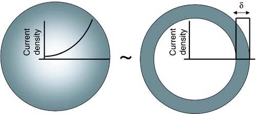
Figure 6-22. Left: Current distribution in a solid rod of copper at some frequency, showing the concentration of current near the outer surface. Darker color is high-current density. Right: Approximating the current in the rod in terms of a uniform current distribution with a thickness equal to the skin depth.
In this geometry, we can approximate the shell of current as a uniform distribution with a fixed thickness, a distance δ, from the outer surface. We call this equivalent thickness of the current shell, the skin depth. It depends on the frequency, the conductivity of the metal, and the permeability of the metal:
where:
δ = skin depth, in meters
σ = conductivity of conductor, in Siemens/m
µ0 = permeability of free space, 4 × π × 10-7 H/m
µr = relative permeability of the conductor
f = sine-wave frequency, in Hz
For the case of copper with a conductivity of 5.6 × 10⁷ Siemens/m and relative permeability of 1, the skin depth is approximately:
where:
δ = the skin depth, in microns
f = the sine-wave frequency, in MHz
At 1 MHz, the skin depth in copper is 66 microns. In Figure 6-23, the skin depth for copper is plotted and compared to the geometrical thickness of 1-ounce and 1/2-ounce copper. This points out that for 1-ounce copper traces, when the sine-wave frequency of the current is higher than about 10 MHz, the current distribution is determined by skin depth; not the geometrical cross section. Below 10 MHz, the current distribution will be uniform and independent of frequency. When the skin depth is thinner than the geometrical cross section, the current distribution, the resistance, and the loop inductance will be frequency dependent.
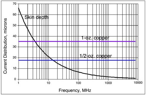
Figure 6-23. Current distribution in copper when skin depth is limited and compared with the geometrical thickness of 1-ounce and 1/2-ounce copper.
This is a handy rule of thumb to keep in mind. This means that if we have a board with 1-ounce copper traces or a geometrical thickness of 34 microns, current that is moving through the conductor at 10-MHz or higher sine-wave frequencies would not use the entire cross section of the trace. It would be dominated by these skin-depth effects.
In real interconnects, there is always a signal path and a return path. As the current loop propagates down the signal and return path, it is the loop self-inductance that influences the impedance the current sees. As frequency increases, the impedance from the loop self-inductance will increase and the current in both conductors will redistribute to take the path of lowest impedance or lowest loop self-inductance. What is the current distribution for lowest loop self-inductance?
There are two ways the loop self-inductance can be decreased: by spreading out the current within each conductor and by bringing the return current closer to the signal current. This will decrease the partial self-inductance of each conductor and increase the partial mutual inductance between them. Both effects will happen: current will spread out within each conductor and the current distribution in both conductors will redistribute so the two currents get closer to each other. The precise current distribution in each conductor is determined by the balance of two forces. Within each conductor, the current wants to spread apart to decrease its partial self-inductance. At the same time, the current in one conductor wants to get as close as possible to the current in the other conductor to increase their partial mutual inductance. The resulting current distribution can only be calculated with a 2D field solver. Figure 6-24 shows the simulated current distribution in a pair of 20-mil (500-micron) diameter ribbon wires. At low frequency, the skin depth is large compared with the geometrical cross section and the current is uniformly distributed in each conductor. At 100 kHz, the skin depth in copper is about 10 mils (250 microns) and is comparable with the cross section, so it will begin to redistribute. At 1 MHz, the skin depth is 2.5 mils (66 microns), small compared to the diameter. The current distribution will be dominated by the skin depth. As the frequency increases, the current redistributes to minimize the loop impedance.

Figure 6-24. Current distribution in 20-mil-diameter wire at three different frequencies and 1-ounce copper microstrip. The lighter the color the higher the current density. Simulated with Ansoft's 2D Extractor.
Also shown is the current distribution for a 1-ounce copper microstrip. At 1 MHz, the current is mostly uniformly distributed. At 10 MHz, it begins to redistribute. Above 10 MHz, the skin depth is much smaller than the cross section and will dominate the current distribution. In both examples, the current redistributes at higher frequency to minimize the impedance.
As the frequency increases, the bulk resistivity of the conductor does not change. For copper, the bulk resistivity doesn't begin to change until above 100 GHz. However, if the current travels through a thinner cross section due to skin-depth effects, the resistance of the interconnect will increase.
TIP
In the skin-depth regime, when the skin depth is thinner than the geometrical cross section, as frequency increases, the cross-sectional area the current travels through decreases proportionally to the square root of the frequency. This will cause the resistance per length of the line to increase with the square root of the frequency as well.
Consider the case of a simple microstrip line, made from 1-ounce copper, 5 mils wide. The resistance per length of the signal path at DC frequency is:
where:
RDC = the resistance per length for DC currents
ρ = the bulk resistivity of copper
w = the line width of the signal trace
t = the geometrical thickness of the signal trace
At frequencies above about 10 MHz, the current is skin-depth limited and the resistance will be frequency dependent. Above this frequency, the thickness of the conductor that is actually being used by the current is roughly the skin depth, so the high-frequency resistance is really:
where:
RHF = the resistance per length for high-frequency currents
ρ = the bulk resistivity of copper
w = the line width of the signal trace
δ = the skin depth of copper at the high frequency
The ratio of resistance at high frequency to the resistance at DC is roughly RHF/RDC = t/δ. At 1 GHz, where the skin depth of copper is 2 microns, the high-frequency resistance will be 30 microns/2 microns = 15 × higher than the low-frequency resistance for 1-ounce copper. The series resistance of a signal trace will only get larger at higher frequencies.
Figure 6-25 shows the measured resistance of a small loop of 22-gage copper wire, 25 mils in thickness. The loop was about 1 inch in diameter. The skin depth is comparable to the geometrical thickness at 10 kHz. At higher frequencies, the resistance should increase with roughly the square root of frequency.
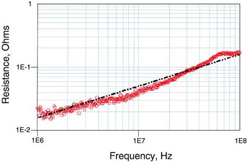
Figure 6-25. Measured series resistance of a 22-gage copper wire loop, 1 inch in diameter, showing the resistance increasing with the square root of frequency. Circles are measured resistance; the line is resistance increasing with the square root of frequency.
One consequence of the frequency-dependent current distribution is the frequency-dependent resistance. In addition, the inductance will change. Since the driving force for the current redistribution is decreasing loop self-inductance, the loop self-inductance will decrease with higher frequency.
At DC frequency, the self-inductance of a wire will be composed of the external self-inductance and the internal self-inductance. The external self-inductance will not change as the current redistributes within the conductor, but the internal self-inductance will decrease as more current moves to the outside. At frequencies far above where the skin depth is comparable to the geometrical thickness, there will be very little current inside the conductor and there will be no internal self-inductance.
We would expect the self-inductance of a wire to be frequency dependent. At low frequency, it will be Linternal + Lexternal. At high frequency, it should be simply Lexternal. The transition should start at about where the skin depth is comparable to the geometrical thickness and reach a steady value above a frequency where the skin depth is just a small fraction of the geometrical thickness.
The precise current distribution and the contribution of internal and external self-inductance are hard to estimate analytically, especially for rectangular cross sections. However, they can be calculated very easily using a 2D field solver.
Figure 6-26 shows an example of the loop self-inductance per length for a microstrip as the current redistributes itself. This illustrates that due to skin-depth effects, the low-frequency inductance is higher than the high-frequency inductance by an amount equal to the internal self-inductance. Above about 100 MHz, the current travels in a thin shell, and the inductance is constant with further increase in frequency.
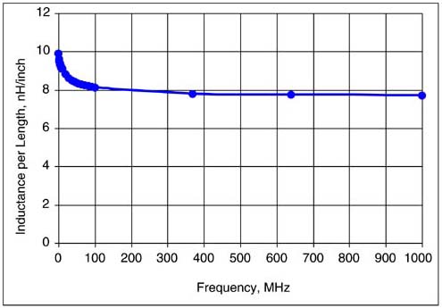
Figure 6-26. Loop self-inductance of a microstrip as the current redistributes due to skin-depth effects, calculated with Ansoft's 2D Extractor.
TIP
When we refer to the loop self-inductance of a microstrip, for example, we are more often referring to this high-frequency limit, assuming all the current is in the outside surface. “High frequency” refers to above the skin-depth limit, where current is close to the surface and not dependent on the geometrical thickness.
There is an important term affecting skin depth that applies to only a few special materials. This term is the permeability of the conductor. Permeability refers to how the conductor interacts with magnetic-field line loops. Most metals have a permeability of 1 and they do not interact with magnetic-field line loops.
However, when the permeability is greater than 1, the number of field line loops in the metal is amplified over what would be there if the permeability were 1. There are only three metals that have a permeability other than 1. These are the ferromagnetic metals: iron, nickel, and cobalt. Most alloys that contain any combination of these metals have a permeability much greater than 1. We are most familiar with ferrites, which usually contain iron and cobalt and can have permeabilities of over 1,000. Two important interconnect metals are ferromagnetic: Alloy 42 and Kovar. The permeability of these metals can be 100–500. This high permeability can have a significant impact on the frequency dependence of the resistance and inductance of an interconnect made from these materials.
For a ferromagnetic wire, at DC frequency, the self-inductance of the wire will be related to the internal and external self-inductance. All the field line loops that contribute to the external self-inductance see only air, which has a permeability of 1. The external self-inductance of a ferromagnetic wire will be exactly the same as if the wire were made of copper. After all, for the same current in the wire, there would be the same external-field line loops per amp of current.
However, the internal-field line loops in the ferromagnetic wire will see a high permeability, and these magnetic-field line loops will be amplified. At low frequency, the inductance of a ferromagnetic wire is very high, but above about 1 MHz, all the field line loops are external and the loop self-inductance is comparable to a copper loop of the same dimension.
TIP
The loop inductance that high-speed signals would encounter in a ferromagnetic conductor is comparable to the loop inductance if the conductor were made from copper, since above the skin-depth limit the loop inductance is composed almost solely of external-field line loops.
The skin depth for a ferromagnetic conductor can be much smaller than for a copper conductor, due to its high permeability. For example, nickel, having a bulk conductivity of about 1.4 × 10⁷ Siemens/m and permeability of about 100, has a skin depth of roughly:
At the same frequency, the cross section for current in a nickel conductor will be much thinner than for an equivalent-geometry copper conductor. In addition, the bulk resistivity is higher. This means the series resistance will be much higher. Figure 6-27 shows the measured series resistance of 1-inch-diameter loops of copper wire and nickel wire of roughly comparable cross section. The resistance of the nickel wire is more than 10 times higher than that of the copper wire and is clearly increasing with the square root of frequency, which is characteristic of a skin-depth-limited current distribution. This is why the high-frequency resistance of Kovar or Alloy 42 leads can be very high compared to nonferromagnetic leads.
Figure 6-27. Measured resistance of 1-inch-diameter loops of copper wire and nickel wire, of roughly the same cross section, showing much higher resistance of the nickel conductor, due to skin-depth effects. The resistance increases with the square root of frequency, shown by the superimposed line. The noise floor of the measurement was about 10 milliOhms.
Surface microstrip traces on circuit boards are often plated on their top surface with a nickel/gold layer to facilitate solder-attach of components. This nickel layer has virtually no impact on the electrical properties of the trace because it is on the other side of the trace from the return path. The current will travel the path of lowest impedance, which is not through the nickel layer. If the conductor were solid nickel, the resistance and inductance would be strongly frequency dependent. With the thick copper on one side, all the current can flow through the lower-impedance path in the copper.
This is why a plating of silver is sometimes applied to Alloy 42 leads to limit their resistance at high frequency. It provides a nonferromagnetic conductor on the outer surface for high-frequency currents to travel. The highest frequency components will experience a larger-skin-depth and higher-conductivity material.
The precise resistance of a conductor will depend on the frequency-dependent current distribution, which, for arbitrary shapes, may be difficult to calculate. This is one of the values of a good 2D field solver that allows the calculation of frequency-dependent current distributions and the resulting inductance and resistance.
As mentioned previously, if there are two conductors and the current in one changes, there will be a voltage created across the second, due to the changing mutual magnetic-field line loops around it. This voltage induced in the second conductor can drive currents in the second conductor. In other words, changing the current in one conductor can induce current in the second conductor. We call the induced currents in the second conductor eddy currents.
There is an important geometry where eddy currents can significantly affect the partial self-inductance of a conductor and the loop self-inductance of a current loop. This geometry occurs when a loop is near a large conducting surface, such as a plane in a circuit board or the sides of a metal enclosure.
As the simplest example, consider a round wire above a metal plane. It is important to keep in mind that this metal plane can be any conductor and can float at any voltage. It does not matter what its voltage is, or what else it is connected to. All that is important is that it is conductive and that it is continuous.
When there is current in the wire, some of the field line loops will pass through the conducting plane. There will be some mutual inductance between the wire and the plane. When current in the wire changes, some of the magnetic-field line loops going through the plane will change and voltages will be induced in the plane. These voltages will drive eddy currents in the plane. These eddy currents will, in turn, produce their own magnetic fields.
By solving Maxwell's Equations, it can be shown that the pattern of the magnetic-field line loops generated by the eddy currents looks exactly like the magnetic-field lines from another current that would be located below the surface of the plane (i.e., a distance below equal to the height above the plane of the real current). This is illustrated in Figure 6-28. This fictitious current is called an image current. The direction of the image current is opposite the direction of the real current that induced it. The net magnetic-field lines from the real current and the induced eddy currents will have the same field line distribution as from the real current and the image current, as though the plane were not there. To understand the actual magnetic-field line loops present with the combination of the real current and the induced eddy currents, we can throw out the plane and the real eddy currents and replace them with the image current. The field line loops from the real current and the image current will be exactly the same as the field line loops from real current and the eddy currents.

The current in the image current is exactly the same magnitude as the current in the real current, but in the opposite direction. Some of the field line loops from the image current will go around the real current. But, because the direction of the image current is opposite the direction of the source current, the field line loops from the image current will subtract from the field line loops around the real current.
This has the unusual effect of decreasing the partial self-inductance of the wire. If a current loop is over the surface of a floating, conducting plane, which has absolutely no electrical contact to the loop, the mere presence of the plane will decrease the loop inductance of the loop. The closer the wire is to the plane, the closer is the image current, and the more mutual-field line loops there are from the image current, and the lower the partial self-inductance of the real current. The closer the floating plane below, the larger the induced eddy currents in the plane and the greater the reduction of the self-inductance of the signal path. Figure 6-29 shows the eddy current distributed in an adjacent plane when the signal path is in proximity to the floating plane.
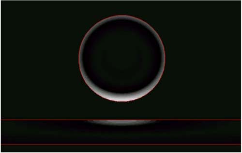
Figure 6-29. Current distribution at 1 MHz in a round conductor near a floating plane showing the eddy currents induced in the plane.
When two long, rectangular coplanar conductors make up a signal and return path loop, they will have some loop self-inductance per length. If a uniform, floating conducting plane is brought in proximity, their loop self-inductance will decrease due to the field line loops from the eddy currents in the plane below. The closer the plane, the lower the loop inductance. Figure 6-30 shows this reduction in loop self-inductance per length for a simple case.

Figure 6-30. Top: current distribution in the two legs of a long rectangular coplanar loop, showing the induced eddy currents in the floating plane. Bottom: the change in loop self-inductance per length as the distance to the floating plane changes, calculated with Ansoft's 2D Extractor.
In this example, the line width is 5 mils and the spacing is 10 mils. The span between the outer edges of each conductor is 20 mils. As a rough rule of thumb, the induced eddy currents will play a role if the spacing to the floating plane is closer than the total span of the conductors.
Inductance is a critically important term that affects all aspects of signal integrity.
The basic definition of inductance is that it is the number of magnetic-field line loops around a conductor per amp of current through the conductor.
All the various types of inductance are special qualifiers that specify from which conductor the field line loops arise (self and mutual), about how much of the conductor the field line loops are counted (partial and loop) and if all the field line loops are included, even those from the rest of the loop (total).
The only reason inductance is important is because of induced voltage: if the number of field line loops around a conductor changes, a voltage is induced across the ends of the conductor related to how fast the field line loops change.
Ground bounce is the voltage induced between different parts of the ground-return path due to a total inductance of the return path and a dI//dt through it.
Reducing ground bounce is about reducing the total inductance of the return path: wide conductors, short lengths, and the signal path as close as possible to the return path.
Lowest rail-collapse noise is obtained when the loop inductance from the chip pad to the decoupling capacitor is as low as possible. The lowest loop inductance interconnect is two wide planes as close together as possible.
The loop inductance between two planes is increased by the presence of a field of via holes. For the case of about 50% open area, the loop inductance is increased by about 25%.
As the sine-wave frequency components of currents increase, they will take the path of lowest impedance which translates to a distribution toward the outside surface of the conductors and signal and return currents as close together as possible. This causes the inductance to be slightly frequency dependent, decreasing toward higher frequency, and the resistance to be strongly frequency dependent, increasing with the square root of the frequency.
When a current is in proximity to a uniform plane, even if it is floating, induced eddy currents will cause the self-inductance of the current to decrease.