
In high-speed digital systems, where signal integrity plays a significant role, we often refer to signals as either changing voltages or a changing currents. All the effects that we lump in the general category of signal integrity are due to how analog signals (those changing voltages and currents) interact with the electrical properties of the interconnects. The key electrical property with which signals interact is the impedance of the interconnects.
Impedance is defined as the ratio of the voltage to the current. We usually use the letter Z to represent impedance. The definition, which is always true, is Z = V/I. The manner in which these fundamental quantities, voltage and current, interact with the impedance of the interconnects determines all signal-integrity effects. As a signal propagates down an interconnect, it is constantly probing the impedance of the interconnect and reacting based on the answer.
TIP
If we know the impedance of the interconnect, we can accurately predict how the signals will be distorted and whether a design will meet the performance specification, before we build it.
Likewise, if we have a target spec for performance and know what the signals will be, we can sometimes specify an impedance specification for the interconnects. If we understand how the geometry and material properties affect the impedance of the interconnects, then we will be able to design the cross section, the topology, and the materials and select the other components so they will meet the impedance spec and result in a product that works the first time.
TIP
Impedance is the key term that describes every important electrical property of an interconnect. Knowing the impedance and propagation delay of an interconnect is to know almost everything about it electrically.
Each of the four basic families of signal-integrity problems can be described based on impedance.
Signal-quality problems arise because voltage signals reflect and are distorted whenever the impedance the signal sees changes. If the impedance the signal sees is always constant, there will be no reflection and the signal will continue undistorted. Attenuation effects are due to series and shunt-resistive impedances.
Cross talk arises from the electric and magnetic fields coupling between two adjacent signal traces (and, of course, their return paths). The mutual capacitance and mutual inductance between the traces establishes an impedance, which determines the amount of coupled current.
Rail collapse of the voltage supply is really about the impedance in the power-distribution system (PDS). A certain amount of current must flow to feed all the ICs in the system. Because of the impedance of the power and ground distribution, a voltage drop will occur as the IC current switches. This voltage drop means the power and ground rails have collapsed from their nominal values.
The greatest source of EMI is from common-mode currents, driven by voltages in the ground planes, through external cables. The higher the impedance of the return current paths in the ground planes, the greater the voltage drop, or ground bounce, which will drive the radiating currents. The most common fix for EMI from cables is the use of a ferrite choke around the cable. This works by increasing the impedance the common-mode currents see, thereby reducing the amount of common-mode current.
There are a number of design rules, or guidelines, that establish constraints on the physical features of the interconnects. For example, “keep the spacing between adjacent signal traces greater than 10 mils” is a design rule to minimize cross talk. “Use power and ground planes on adjacent layers separated by less than 5 mils” is a design rule for the power and ground distribution.
TIP
Not only are the problems associated with signal integrity best described by the use of impedance, but the solutions and the design methodology for good signal integrity are also based on the use of impedance.
These rules establish a specific impedance for the physical interconnects. This impedance provides a specific environment for the signals, resulting in a desired performance. For example, keeping the power and ground planes closely spaced will result in a low impedance for the power distribution system and hence a lower voltage drop for a given power and ground current. This helps minimize rail collapse and EMI.
If we understand how the physical design of the interconnects affects their impedance, we will be able to interpret how they will interact with signals and what performance they might have.
TIP
Impedance is the Rosetta stone that links physical design and electrical performance. Our strategy is to translate system-performance needs into an impedance requirement and physical design into an impedance property.
Impedance is at the heart of the methodology we will use to solve signal-integrity problems. Once we have designed the physical system as we think it should be for optimal performance, we will translate the physical structure into its equivalent electrical circuit model. This process is called modeling.
It is the impedance of the resulting circuit model that will determine how the interconnects will affect the voltage and current signals. Once we have the circuit model, we will use a circuit simulator, such as SPICE, to predict the new waveforms as the voltage sources are affected by the impedances of the interconnects. Alternatively, behavioral models of the drivers or interconnects can be used where the interaction of the signals with the impedance, described by the behavioral model, will predict performance. This process is called simulation.
Finally, the predicted waveforms will be analyzed to determine if they meet the timing and distortion or noise specs, and are acceptable, or if the physical design has to be modified. This process flow for a new design is illustrated in Figure 3-1.
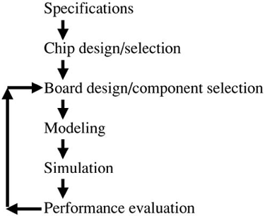
Figure 3-1. Process flow for hardware design. The modeling, simulation, and evaluation steps should be implemented as early and often in the design cycle as possible.
The two key processes, modeling and simulation, are based on converting electrical properties into an impedance, and analyzing the impact of the impedance on the signals.
If we understand the impedance of each of the circuit elements used in a schematic and how the impedance is calculated for a combination of circuit elements, the electrical behavior of any model and any interconnect can be evaluated. This concept of impedance is absolutely critical in all aspects of signal-integrity analysis.
We use the term impedance in everyday language and often confuse the electrical definition with the common usage definition. As we saw earlier, the electrical term impedance has a very precise definition based on the relationship between the current through a device and the voltage across it: Z = V/I. This basic definition applies to any two-terminal device, such as a surface mount resistor, a decoupling capacitor, a lead in a package, or the front connections to a printed circuit-board trace and its return path. When there are more than two terminals, such as in coupled conductors, or between the front and back ends of a transmission line, the definition of impedance is the same, it's just more complex to take into account the additional terminals.
For two-terminal devices, the definition of impedance, as illustrated in Figure 3-2, is simply:
where:
Z = the impedance, measured in Ohms
V = the voltage across the device, in units of volts
I = the current through the device, in units of Amps

Figure 3-2. The definition of impedance for any two-terminal device showing the current through the component and the voltage across the leads.
For example, if the voltage across a terminating resistor is 5 v and the current through it is 0.1 A, then the impedance of the device must be 5 v/0.1 A = 50 Ohms. No matter what type of device the impedance is referring to, in both the time and the frequency domain, the units of impedance are always in Ohms.
TIP
This definition of impedance applies to absolutely all situations, whether in the time domain or the frequency domain, whether for real devices that are measured or for ideal devices that are calculated.
If we always go back to this basic definition, we will never go wrong and oftentimes eliminate many sources of confusion. One aspect of impedance that is often confusing is to think of it only in terms of resistance. As we shall see, the impedance of an ideal resistor-circuit element, with resistance, R, is, in fact, Z = R.
Our intuition of the impedance of a resistor is that a high impedance means less current flow for a fixed voltage. Likewise, a low impedance means a lot of current can flow for the same voltage. This is consistent with the definition that I = V/Z, and applies just as well when the voltage or current is not DC.
In addition to the notion of the impedance of a resistor, the concept of impedance can apply to an ideal capacitor, an ideal inductor, a real-wire bond, a printed circuit trace, or even a pair of connector pins.
There are two special extreme cases of impedance. For a device that is an open, there will be no current flow. If the current through the device for any voltage applied is zero, the impedance is Z = 1 v / 0 A = infinite Ohms. The impedance of an open device is very, very large. When the device is a short, there will be no voltage across it, no matter what the current through it. The impedance of a short is Z = 0 v / 1 A = 0 Ohms. The impedance of a short is always 0 Ohms.
There are two types of electrical devices, real and ideal. Real devices can be measured. They are the only things that physically exist. They are the actual interconnects or components that make up the hardware of a real system. Real devices are traces on a board, leads in a package, or discrete decoupling capacitors mounted to a board.
Ideal devices are mathematical descriptions of specialized circuit elements that have precise, specific definitions. Simulators can only simulate the performance of ideal devices. The formalism and power of circuit theory apply only to ideal devices. Models are composed of combinations of ideal devices.
It is very important to keep separate real versus ideal circuit elements. The impedance of any real, physical interconnect or passive component can be measured. However, when impedance is calculated, it is only the impedance of four very-well-defined, ideal circuit elements that can be considered. We cannot measure ideal circuit elements, nor can we calculate the impedance of any circuit elements other than ideal ones. This is why it is important to make the distinction between real components and ideal circuit elements. This distinction is illustrated in Figure 3-3.
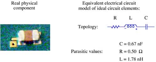
Figure 3-3. The two worldviews of a component, in this case a 1206 decoupling capacitor mounted to a circuit board and an equivalent circuit model composed of combinations of ideal circuit elements.
TIP
Ultimately, our goal is to create an equivalent circuit model composed of combinations of ideal circuit elements whose impedance closely approximates the actual, measured impedance of a real component.
A circuit model will always be an approximation of the real-world structure. However, it is possible to construct an ideal model with a simulated impedance which accurately matches the measured impedance of a real device. For example, Figure 3-4 shows the measured impedance of a real decoupling capacitor and the simulated impedance based on an RLC circuit model. These are the component and model in Figure 3-3. The agreement is excellent even up to 5 GHz, the bandwidth of the measurement.
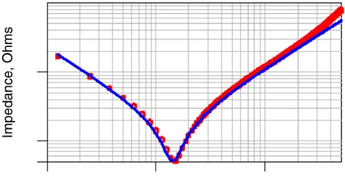
Figure 3-4. The measured impedance, as circles, and the simulated impedance, as the line, for a nominal 1-nF decoupling capacitor. The measurement was performed with a network analyzer and a GigaTest Labs Probe Station.
There are four ideal, two-terminal, circuit elements that we will use in combination as building blocks to describe any real interconnect:
A resistor
A capacitor
An inductor
A transmission line
We usually group the first three elements in a category called “lumped circuit elements,” in the sense that their properties can be lumped into a single point. This is different from the properties of an ideal transmission line, which are “distributed” along its length.
As ideal circuit elements, these elements have precise definitions that describe how they interact with currents and voltages. It is very important to keep in mind that ideal elements are different from real components, such as real resistors, real capacitors, or real inductors. One is a physical component, the other an ideal element.
The properties of a transmission line are initially seen as so confusing and non-intuitive, yet so important, that we devote an entire chapter to transmission lines and their impedance. In this chapter, we will concentrate on the impedance of just R, L, and C elements.
An equivalent electrical circuit model is an idealized electrical description of a real structure. It is an approximation, based on using combinations of ideal circuit elements. A good model will have a calculated impedance that closely matches the measured impedance of the real device. The better we can model the impedance of an interconnect, the better we can predict how a signal will interact with it.
When dealing with some high-frequency effects, such as lossy lines, we will need to invent new ideal circuit elements to create better models.
Each of the four basic circuit elements above has a definition of how voltage and current interact with it. This is different from the impedance of the ideal circuit element.
The relationship between the voltage across and the current through an ideal resistor is:
where:
V = the voltage across the ends of the resistor
I = the current through the resistor
R = the resistance of the resistor, in Ohms
An ideal resistor has a voltage across it that increases with the current through it. This definition of the I-V properties of an ideal resistor applies in both the time domain and the frequency domain.
In the time domain, we can apply the definition of the impedance and, using the definition of the ideal element, calculate the impedance of an ideal resistor:
This basically says, the impedance is constant and independent of the current or voltage across a resistor. The impedance of a resistor is pretty boring.
In an ideal capacitor, there is a relationship between the charge stored between the two leads and the voltage across the leads. The capacitance of an ideal capacitor is defined as:
where:
C = the capacitance, in Farads
V = the voltage across the leads, in volts
Q = the charge stored between the leads, in Coulombs
The value of the capacitance of a capacitor describes its capacity to store charge at the expense of voltage. A large capacitance means the ability to store a lot of charge at a low voltage across the terminals.
The impedance of a capacitor can only be calculated based on the current through it and the voltage across its terminals. In order to relate the voltage across the terminals with the current through it, we need to know how the current flows through a capacitor. A real capacitor is made from two conductors separated by a dielectric. How does current get from one conductor to the other, when it has an insulating dielectric between them? This is a fundamental question and will pop up over and over in signal integrity applications.
The answer is that real current probably doesn't really flow through a capacitor, it just acts as though it does when the voltage across the capacitor changes. Suppose the voltage across a capacitor were to increase. This means that some positive charge had to be added to the top conductor and some negative charge had to be added to the bottom conductor. Adding negative charge to the bottom conductor is the same as pushing positive charge out; it is as though positive charges were added to the top terminal and positive charges were pushed out of the bottom terminal. This is illustrated in Figure 3-5. The capacitor behaves as though current flows through it, but only when the voltage across it changes.
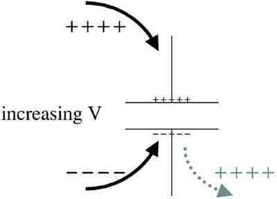
Figure 3-5. Increasing the voltage across a capacitor adds positive charge to one conductor and negative charge to the other. Adding negative charge to one conductor is the same as taking positive charges from it. It looks like positive charge enters one terminal and comes out of the other.
By taking derivatives of both sides of the previous equation, a new definition of the I-V behavior of a capacitor can be developed:
where:
I = the current through the capacitor
Q = the charge on one conductor of the capacitor
C = the capacitance of the capacitor
V = the voltage across the capacitor
This relationship points out, as we saw previously, that the only way current flows through a capacitor is when the voltage across it changes. If the voltage is constant, the current through a capacitor is zero. We also saw that for a resistor, the current through it doubled if the current doubled. However, in the case of a capacitor, the current through it doubles if the rate of change of the voltage across it doubles.
This definition is consistent with our intuition. If the voltage changes rapidly, the current through a capacitor is large. If the voltage is nearly constant, the current through a capacitor is near zero. Using this relationship, we can calculate the impedance of an ideal capacitor in the time domain:
where:
V = the voltage across the capacitor
C = the capacitance of the capacitor
I = the current through the capacitor
This is a complicated expression. It says that the impedance of a capacitor depends on the precise shape of the voltage waveform across it. If the slope of the waveform is large (i.e., if the voltage changes very fast), the current through it is high and the impedance is small. It also says that a large capacitor will have a lower impedance than a small capacitor for the same rate of change of the voltage signal.
However, the precise value of the impedance of a capacitor is more complicated. It is hard to generalize what the impedance of a capacitor is other than it depends on the shape of the voltage waveform. The impedance of a capacitor is not an easy term to use in the time domain.
The behavior of an ideal inductor is defined by:
where:
V = the voltage across the inductor
L = the inductance of the inductor
I = the current through the inductor
This says that the voltage across an inductor depends on how fast the current through it changes. If the current is constant, the voltage across the inductor will be zero. Likewise, if the current changes rapidly through an inductor, there will be a large voltage drop across it. The inductance is the proportionality constant that says how sensitive the voltage generated is to a changing current. A large inductance means that a small changing current produces a large voltage.
There is often confusion about the direction of the voltage drop that is generated across an inductor. If the direction of the changing current reverses, the polarity of the induced voltage will reverse. An easy way of remembering the polarity of the voltage is to base it on the voltage drop of a resistor.
If a DC current goes through a resistor, the terminal the current goes into is the positive side and the other terminal is the negative side. Likewise, with an inductor, the terminal the current is increasing into is the positive side and the other is the negative side for the induced voltage. This is illustrated in Figure 3-6.
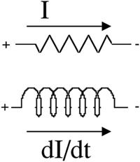
Figure 3-6. The direction of voltage drop across an inductor for a changing current is in the same direction as the voltage drop across a resistor for a DC current.
Using this basic definition of inductance, we can calculate the impedance of an inductor. This is, by definition, the ratio of the voltage to the current through an inductor:

where:
V = the voltage across the inductor
L = the inductance of the inductor
I = the current through the inductor
Again, we see the impedance of an inductor, though well defined, is awkward to use in the time domain. The general features are easy to discern. If the current through an inductor increases rapidly, the impedance of the inductor is large. An inductor will have a high impedance when current through it tries to change. If the current through an inductor changes only slightly, its impedance will be very small. For DC current the impedance of an inductor is nearly zero. But, other than these simple generalities, the actual impedance of an inductor depends very strongly on the precise waveform of the current through it.
TIP
For both the capacitor and the inductor, the impedance, in the time domain, is not a simple function at all. Impedance in the time domain is a very complicated way of describing these basic building-block ideal circuit elements. It is not wrong, it is just complicated.
This is one of the important occasions where moving to the frequency domain will make the analysis of a problem much simpler.
The important feature of the frequency domain is that the only waveforms that can exist are sine waves. We can only describe the behavior of ideal circuit elements in the frequency domain by how they interact with sine waves: sine waves of current and sine waves of voltage. These sine waves have three and only three features: the frequency, the amplitude, and the phase associated with each wave.
Rather than describe the phase in cycles or degrees, it is more common to use radians. There are 2 x π radians in one cycle, so a radian is about 57 degrees. The frequency in radians per second is referred to as the angular frequency. The Greek letter omega (ω) is used to denote the angular frequency. ω is related to the frequency, by:
where:
ω = the angular frequency, in radians/sec
f = the sine-wave frequency, in Hertz
We can apply sine-wave voltages across a circuit element and look at the sine waves of current through it. When we do this, we will still use the same basic definition of impedance (that is, the ratio of the voltage to the current) except that we will be taking the ratio of two sine waves, a voltage sine wave and a current sine wave.
It is important to keep in mind that all the basic building-block circuit elements and all the interconnects are linear devices. If a voltage sine wave of 1 MHz, for example, is applied across any of the four ideal circuit elements, the only sine-wave-frequency components that will be present in the current waveform will be a sine wave at 1 MHz. The amplitude of the current sine wave will be some number of Amps and it will have some phase shift with respect to the voltage wave, but it will have exactly the same frequency. This is illustrated in Figure 3-7.
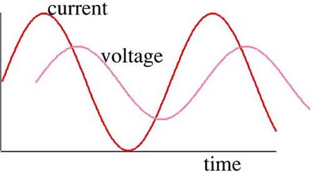
Figure 3-7. The sine-wave current through and voltage across an ideal circuit element will have exactly the same frequency but different amplitudes and some phase shift.
TIP
When we take the ratio of two sine waves, we need to account for the ratio of the amplitudes and the phase shift between the two waves.
What does it mean to take the ratio of two sine waves, the voltage and the current? The ratio of two sine waves is not a sine wave. It is a pair of numbers that contains information about the ratio of the amplitudes and the phase shift, at each frequency value. The magnitude of the ratio is just the ratio of the amplitudes of the two sine waves:
The ratio of the voltage amplitude to the current amplitude will have units of Ohms. We refer to this ratio as the magnitude of the impedance. The phase of the ratio is the phase shift between the two waves. The phase shift has units of degrees or radians. In the frequency domain, the impedance of a circuit element or combination of circuit elements would be of the form: at 20 MHz, the magnitude of the impedance is 15 Ohms and the phase of the impedance is 25 degrees. This means the impedance is 15 Ohms and the voltage wave is leading the current wave by 25 degrees.
The impedance of any circuit element is two numbers, a magnitude and a phase, at every frequency value. Both the magnitude of the impedance and the phase of the impedance may be frequency dependent. The ratio of the amplitudes may vary with frequency or the phase may vary with frequency. When we describe the impedance, we need to specify at what frequency we are describing the impedance.
In the frequency domain, impedance can also be described with complex numbers. For example, the impedance of a circuit can be described as having a real component and an imaginary component. The use of real and imaginary components allows the powerful formalism of complex numbers to be applied, which dramatically simplifies the calculations of impedance in large circuits. Exactly the same information is contained in the magnitude and the phase information. These are two different and equivalent ways of describing impedance.
With this new idea of working in the frequency domain, and dealing only with sine waves of current and voltage, we can take another look at impedance.
We apply a sine wave of current through a resistor and we get a sine wave of voltage across it that is simply R times the current wave:
We can describe the sine wave of current in terms of sine and cosine waves or in terms of complex exponential notation.
When we take the ratio of the voltage to the current for a resistor, we find that it is simply the value of the resistance:
The impedance is independent of frequency and the phase shift is zero. The impedance of an ideal resistor is flat with frequency. This is basically the same result we saw in the time domain, still pretty boring.
When we look at an ideal capacitor in the frequency domain, we will apply a sine-wave voltage across the ends. The current through the capacitor is the derivative of the voltage, which is a cosine wave:
This says the current amplitude will increase with frequency, even if the voltage amplitude stays constant. The higher the frequency, the larger the amplitude of the current through the capacitor. This suggests the impedance of a capacitor will decrease with increasing frequency. The impedance of a capacitor is calculated from:
Here is where it gets confusing. This ratio is easily described using complex math, but most of the insight can also be gained from sine and cosine waves. The magnitude of the impedance of a capacitor is just 1/ωC. All the important information is here. As the angular frequency increases, the impedance of a capacitor decreases. This says that even though the value of the capacitance is constant with frequency, the impedance gets smaller with higher frequency. We see this is reasonable because the current through the capacitor will increase with higher frequency and hence its impedance will be less.
The phase of the impedance is the phase shift between a sine and cosine wave, which is –90 degrees. When described in complex notation, the –90 degree phase shift is represented by the complex number, –i. In complex notation, the impedance of a capacitor is –i/ωC. For most of the following discussion, the phase adds more confusion than value and will generally be ignored.
A real decoupling capacitor has a capacitance of 10 nF. What is its impedance at 1 GHz? First, we assume this capacitor is an ideal capacitor. A 10-nF ideal capacitor will have an impedance of 1/(2 π × 1 GHz × 10 nF) = 1/(6 × 109 × 10 x 10-9) = 1/60 ~ 0.016 Ohms. This is a very small impedance. If the real decoupling capacitor behaved like an ideal capacitor, its impedance would be about 10 milliOhms at 1 GHz. Of course, at lower frequency, its impedance would be higher. At 1 Hz, its impedance would be about 16 MegaOhms.
Let's use this same frequency-domain analysis with an inductor. When we apply a sine wave current through an inductor, the voltage generated is:
This says that for a fixed current amplitude, the voltage across an inductor gets larger at higher frequency. It takes a higher voltage to push the same current amplitude through an inductor. This would hint that the impedance of an inductor increases with frequency.
Using the basic definition of impedance, the impedance of an inductor in the frequency domain can be derived as:
The magnitude of the impedance increases with frequency, even though the value of the inductance is constant with frequency. It is a natural consequence of the behavior of an inductor that it is harder to shove AC current through it with increasing frequency.
The phase of the impedance of an inductor is the phase shift between the voltage and the current which is +90 degrees. In complex notation, a +90 degree phase shift is i. The complex impedance of an inductor is Z = iωL.
In a real decoupling capacitor, there is inductance associated with the intrinsic shape of the capacitor and its board-attach footprint. A rough estimate for this intrinsic inductance is 2 nH. We really have to work hard to get it any lower than this. What is the impedance of just the series inductance of the real capacitor that we will model as an ideal inductor of 2 nH, at a frequency of 1 GHz?
The impedance is Z = 2 × π × 1 GHz × 2 nH = 12 Ohms. When it is in series with the power and ground distribution and we want a low impedance, for example less than 0.1 Ohms, 12 Ohms is a lot. How does this compare with the impedance of the ideal-capacitor component of the real decoupling capacitor? In the last problem, the impedance of the ideal capacitor element at 1 GHz was 0.01 Ohm. The impedance of the ideal inductor component is more than 1000 times higher than this and will clearly dominate the high-frequency behavior of a real capacitor.
We see that for both the ideal capacitor and inductor, the impedance in the frequency domain has a very simple form and is easily described. This is one of the powers of the frequency domain and why we will often turn to it to help solve problems.
The value of the resistance, capacitance, and inductance of ideal resistors, capacitors, and inductors are all constant with frequency. For the case of an ideal resistor, the impedance is also constant with frequency. However, for a capacitor, its impedance will decrease with frequency, and for an inductor, its impedance will increase with frequency.
The impedance behavior of real interconnects can be closely approximated by combinations of these ideal elements. A combination of ideal circuit elements is called an equivalent electrical circuit model, or typically, just a model. The drawing of the circuit model is often referred to as a schematic.
An equivalent circuit model has two features: it identifies how the circuit elements are connected together (called the circuit topology) and it identifies the value of each circuit element (referred to as the parameter values or parasitic values).
Chip designers, who like to think they produce drivers with perfect, pristine waveforms, view all interconnects as parasitics in that they can only screw up their wonderful waveforms. To the chip designer, the process of determining the parameter values of the interconnects is really parasitic extraction, and the term has stuck in general use.
TIP
It is important to keep in mind that whenever we draw circuit elements, they are always ideal circuit elements. We will have to use combinations of ideal elements to approximate the actual performance of real interconnects.
There will always be a limit to how well we can predict the actual impedance behavior of real interconnects, using an ideal equivalent circuit model. This limit can often be found only by measuring the actual impedance of an interconnect and comparing it to the predictions based on the simulations of circuits containing these ideal circuit elements.
There are always two important questions to ask of every model: how good is it and what is its bandwidth? Remember, its bandwidth is the highest sine-wave frequency at which we get good agreement between the measured impedance and the predicted impedance. As a general rule, the closer we would like the predictions of a circuit model to be to the actual measured performance, the more complex the model may have to be.
TIP
It is good practice to always start the process of modeling with the simplest model possible and grow in complexity from there.
Take, for example, a real decoupling capacitor and its impedance as measured from one of the capacitor pads, through a via and a plane below it, coming back up to the start of the capacitor. This is the example shown previously in Figure 3-3. We might expect that this real device could be modeled as a simple ideal capacitor. But, at how high a frequency will the real capacitor still behave like an ideal capacitor? The measured impedance of this real device, from 10 MHz to 5 GHz, is shown in Figure 3-8, with the impedance predicted for an ideal capacitor superimposed.
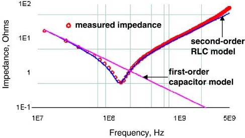
Figure 3-8. Comparison of the measured impedance of a real decoupling capacitor and the predicted impedance of a simple first-order model using a single C element and a second-order model using an RLC circuit model. Measured with a GigaTest Labs Probe Station.
It is clear that this simple model works really well at low frequency. This simple model of an ideal capacitor with a value of 0.67 nF is a very good model. It's just that it gives good agreement only up to about 70 MHz. Its bandwidth is 70 MHz.
If we expend a little more effort, we can create a more accurate circuit model with a higher bandwidth. A more accurate model for a real decoupling capacitor is an ideal capacitor, inductor, and resistor in series. Choosing the best parameter values, we see in Figure 3-8 that the agreement between the predicted impedance of this model and the measured impedance of the real device is excellent, all the way up to the bandwidth of the measurement, 5 GHz in this case.
We often refer to the simplest model we create as a first-order model, as it is the first starting place. As we increase the complexity, and hopefully, better agreement with the real device, we refer to each successive model as the second-order model, third-order model, and so on.
Using the second-order model for a real capacitor would let us accurately predict every important electrical feature of this real capacitor as it would behave in a system with application bandwidths at least up to 5 GHz.
There is a well-defined and relatively straightforward formalism to describe the impedance of combinations of ideal circuit elements. This is usually referred to as circuit theory. The important rule in circuit theory is that when two or more elements are in series, that is, connected end-to-end, the impedance of the combination, from one end terminal to the other end terminal, is the sum of the impedances of each element. What makes it a little complicated is that when in the frequency domain, the impedances that are summed are complex and must obey complex algebra.
In the previous section, we saw that it is possible to calculate the impedance of each individual circuit element by hand. When there are combinations of circuit elements it gets more complicated. For example, the impedance of an RLC model approximating a real capacitor is given by:
We could use this analytic expression for the impedance of the RLC circuit to plot the impedance versus frequency for any chosen values of R, L, and C. It can conveniently be used in a spreadsheet and each element changed. When there are five or ten elements in the circuit model, the resulting impedance can be calculated by hand, but it can be very complicated and tedious.
However, there is a commonly available tool that is much more versatile in calculating and plotting the impedance of any arbitrary circuit. It is so common and so easy to use, every engineer who cares about impedance or circuits in general, should have access to it on their desktop. It is SPICE.
SPICE stands for Simulation Program with Integrated Circuit Emphasis. It was developed in the early 1970s at UC Berkeley as a tool to predict the behavior of transistors based on the as-fabricated dimensions. It is basically a circuit simulator. Any circuit we can draw with R, L, C, and T elements can be simulated for a variety of voltage or current-exciting waveforms. It has evolved and diversified over the past 30 years, with over 30 vendors each adding their own special features and capabilities. There are a few either free versions or student versions for less than $100 that can be downloaded from the Web. Some of the free versions have limited capability but are excellent tools to learn about circuits.
In SPICE, only ideal circuit elements are used and every circuit element has a well-defined, precise behavior. There are two basic types of elements: active and passive. The active elements are the signal sources, current or voltage waveforms, or actual transistor or gate models. The passive elements are all the ideal circuit elements described above. One of the distinctions between the various forms of SPICE is the variety of ideal circuit elements they provide. Every version of SPICE includes at least the R, L, C, and T (transmission-line) elements.
SPICE simulators allow the prediction of the voltage or current at every point in a circuit, simulated either in the time-domain or the frequency domain. A time-domain simulation is called a transient simulation and a frequency-domain simulation is called an AC simulation. SPICE is an incredibly powerful tool.
For example, a driver connected to two receivers located very close together can be modeled with a simple voltage source and an RLC circuit. The R is the impedance of the driver, typically about 10 Ohms. The C is the capacitance of the interconnect traces and the input capacitance of the two receivers, typically about 5 pF total. The L is the total loop inductance of the package leads and the interconnect traces, typically about 7 nH. The set-up of this circuit in SPICE and the resulting time-domain waveform, showing the ringing that might be found in the actual circuit, is shown in Figure 3-9.

Figure 3-9. Simple equivalent circuit model to represent a driver and receiver fanout of two, including the packaging and interconnects, as set up in Agilent's Advanced Design System (ADS), a version of SPICE, and the resulting simulation of the internal-voltage waveform and the voltage at the input of the receivers. The rise time simulated is 0.5 nsec. The lead and interconnect inductance plus the input-gate capacitance dominate the source of the ringing.
TIP
If the circuit schematic can be drawn, SPICE can simulate the voltage and current waveforms. This is the real power of SPICE for general electrical engineering analysis.
SPICE can be used to calculate and plot the impedance of any circuit in the frequency domain. Normally, it plots only the voltage or current waveforms at every connection point, but a trick can be used to convert this into impedance.
One of the circuit elements SPICE has in its toolbox for AC simulation is a constant-current sine-wave-current source. This current source will output a sine wave of current, with a constant amplitude, at a predetermined frequency. When running an AC analysis, the SPICE engine will step the frequency of the sine-wave-current source from the start frequency value to the stop frequency value with a number of intermediate frequency points.
It generates the constant-current amplitude by outputting a sin wave voltage-amplitude sine wave. The amplitude of the voltage wave is automatically adjusted to result in the specified constant amplitude of current.
To build an impedance analyzer in SPICE, we set the current source to have a constant amplitude of 1 Amp. No matter what circuit elements are connected to the current source, SPICE will adjust the voltage amplitude to result in 1-Amp current amplitude through the circuit. If the constant-current source is connected to a circuit that has some impedance associated with it, Z(ω), then to keep the amplitude of the current constant, the voltage it applies will have to adjust. The voltage applied to the circuit, from the constant-current source, with a 1-Amp current amplitude, is V(ω) = Z(ω) × 1 Amp. The voltage across the current source, in volts, is numerically equal to the impedance of the circuit attached, in Ohms.
For example, if we attach a 1-Ohm resistor across the terminals, in order to maintain the constant current of 1 Amp, the voltage amplitude generated must be V = 1 Ohm × 1A = 1 v. If we attach a capacitor with capacitance C, the voltage amplitude at any frequency will be V = 1/ωC. Effectively, this circuit will emulate an impedance analyzer. Plotting the voltage versus the frequency is a measure of the magnitude of the impedance versus frequency for any circuit. The phase of the voltage is also a measure of the phase of the impedance.
To use SPICE to plot an impedance profile, we construct an AC constant-current source with amplitude of 1 A and connect the circuit under test across the terminals. The voltage measured across the current source is a direct measure of the impedance of the circuit. An example of a simple circuit is shown in Figure 3-10. As a trivial example, we connect a few different circuit elements to the impedance analyzer and plot their impedance profiles.
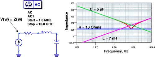
Figure 3-10. Left: An impedance analyzer in SPICE. The voltage across the constant-current source is a direct measure of the impedance of the circuit connected to it. Right: An example of the magnitude of the impedance of various circuit elements, calculated with the impedance analyzer in SPICE.
We can use this impedance analyzer to plot the impedance of any circuit model. Impedance is complex. It has not only magnitude information but also phase information. We can plot each of these separately in SPICE. The phase is also available in an AC simulation in SPICE. In Figure 3-11, we illustrate using the impedance analyzer to simulate the impedance of an RLC circuit model, approximating a real capacitor, plotting the magnitude and phase of the impedance across a wide frequency range.
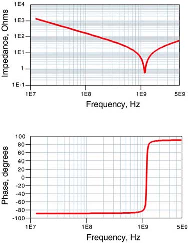
Figure 3-11. Simulated magnitude and phase of an ideal RLC circuit. The phase shows the capacitive behavior at low frequency and the inductive behavior at high frequency.
It is exactly as expected. At low frequency, the phase of the impedance is –90 degrees, suggesting capacitive behavior. At high frequency the phase of the impedance is +90 degrees, suggesting inductive behavior.
As pointed out in Chapter 1, equivalent circuit models for interconnects and passive devices can be created based either on measurements or on calculations. In either case, the starting place is always some assumed topology for the circuit model. How do we pick the right topology? How do we know what is the best circuit schematic with which to start?
The strategy for building models of interconnects or other structures is to follow the principle that Albert Einstein articulated when he said, “Everything should be made as simple as possible, but not simpler.” Always start with the simplest model first, and build in complexity from there.
Building models is a constant balancing act between the accuracy and bandwidth of the model required and the amount of time and effort we are willing to expend in getting the result. In general, the more accuracy required, the more expensive the cost in time, effort, and dollars. This is illustrated in Figure 3-12.
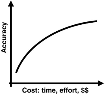
Figure 3-12. Fundamental trade-off between the accuracy of a model and how much effort is required to achieve it. This is a fundamental relationship for most issues in general.
TIP
When constructing models for interconnects, it is always important to keep in mind that sometimes an OK answer, now, is better than a more accurate answer late. This is why Einstein's advice should be followed: start with the simplest model first and build in complexity from there.
When the interconnect structure is electrically short, the simplest circuit model to start with is one composed of lumped circuit elements. When it is uniform and electrically long, the best circuit model to start with is an ideal transmission line model. This property of electrical length is described in a later chapter.
The simplest lumped circuit model is just a single R, L, or C circuit element. The next simplest are combinations of two of them, and then three of them, and so on. The key factor that determines when we need to increase the complexity of a model is the bandwidth of the model required. As a general trend, the higher the bandwidth, the more complex the model. However, every high-bandwidth model must still give good agreement at low frequency; otherwise it will not be accurate for transient simulations that can have low-frequency components in the signals.
For discrete passive devices, such as surface-mount technology (SMT) terminating resistors, decoupling capacitors, and filter inductors, the low-bandwidth and high-bandwidth ideal circuit model topologies are illustrated in Figure 3-13. As we saw earlier for the case of decoupling capacitors, the single-element circuit model worked very well at low frequency. The higher-bandwidth model for a real decoupling capacitor worked even up to 5 GHz for the specific component measured. The bandwidth of a circuit model for a real component is not easy to estimate except from a measurement.
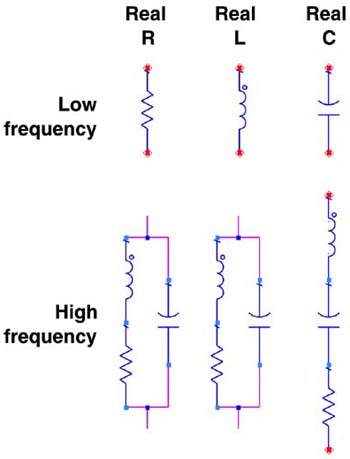
Figure 3-13. Simplest starting models for real components or interconnect elements, at low frequency and for higher bandwidth.
For many interconnects that are electrically short, simple circuit models can also be used. The simplest starting place for a printed-circuit trace over a return plane in the board, which might be used to connect one driver to another, is a single capacitor. Figure 3-14 is an example of the measured impedance of a one-inch interconnect and the simulated impedance of a first-order model consisting of a single C element model. In this case, the agreement is excellent up to about 1 GHz. If the application bandwidth was less than 1 GHz, a simple ideal capacitor could be used to accurately model this one-inch-long interconnect.

Figure 3-14. Measured impedance of a one-inch-long microstrip trace and the simulated impedance of a first- and second-order model. The first-order model is a single C element and has a bandwidth of about 1 GHz. The second-order model uses a series LC circuit and has a bandwidth of about 2 GHz.
For a higher bandwidth model, a second-order model consisting of an inductor in series with the capacitor can be used. The agreement of this higher-bandwidth model is about 2 GHz.
As we show in a later chapter, the best model for an electrically long, uniform interconnect is an ideal transmission line model. This T element works at low frequency and at high frequency. Figure 3-15 illustrates the excellent agreement between the measured impedance and the simulated impedance of an ideal T element across the entire bandwidth of the measurement.
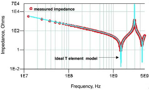
Figure 3-15. Measured impedance of a one-inch-long microstrip trace and the simulated impedance of an ideal T element model. The agreement is excellent up to the full bandwidth of the measurement. Agreement is also excellent at low frequency.
An ideal resistor-circuit element can model the actual behavior of real resistor devices up to surprisingly high bandwidth. There are three general technologies for resistor components, such as those used for terminating resistors: axial lead, SMT, and integrated passive devices (IPDs). The measured impedance of a representative of each technology is shown in Figure 3-16.
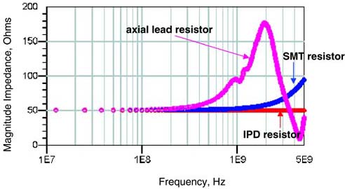
Figure 3-16. Measured impedance of three different resistor components, axial lead, surface-mount (SMT), and integrated passive device (IPD). An ideal resistor element has an impedance constant with frequency. This simple model matches each real resistor at low frequency but has limited bandwidth depending on the resistor technology.
An ideal resistor will have an impedance that is constant with frequency. As can be seen, the IPD resistors match the ideal resistor-element behavior up to the full-measurement bandwidth of 5 GHz. SMT resistors are well approximated by an ideal resistor up to about 2 GHz, depending on the mounting geometry and board stack-up, and axial-lead resistors can be approximated to about 500 MHz by an ideal resistor. In general, the primary effect that arises at higher frequency is the impact from the inductive properties of the real resistors. A higher-bandwidth model would have to include inductor elements and maybe also capacitor elements.
Having the circuit-model topology is only half of the solution. The other half is to extract the parameter values, either from a measurement or with a calculation. Starting with the circuit topology, we can use rules of thumb, analytic approximations, and numerical-simulation tools to calculate the parameter values from the geometry and material properties for each of the circuit elements. This is detailed in the next chapters.
Impedance is a powerful concept to describe all signal-integrity problems and solutions.
Impedance describes how voltages and currents are related in an interconnect or component. It is fundamentally the ratio of the voltage across a device to the current through it.
Real components that make up the actual hardware are not to be confused with ideal circuit elements that are the mathematical description of an approximation to the real world.
Our goal is to create an ideal circuit model that adequately approximates the impedance of the real physical interconnect or component. There will always be a bandwidth beyond which the model is no longer an accurate description, but simple models can work to surprisingly high bandwidth.
The resistance of an ideal resistor, the capacitance of an ideal capacitor, and the inductance of an ideal inductor are all constant with frequency.
Though impedance has the same definition in the time and frequency domains, the description is simpler and easier to generalize for C and L components in the frequency domain.
The impedance of an ideal R is constant with frequency. The impedance of an ideal capacitor varies as 1/ωC and the impedance of an ideal inductor varies as ωL.
SPICE is a very powerful tool to simulate the impedance of any circuit or the voltage and current waveforms expected in both the time and frequency domains. Every engineer who deals with impedance should have a version of SPICE available to him or her on his or her desktop.
When building equivalent circuit models for real interconnects, it is always important to start with the simplest model possible and build in complexity from there. The simplest starting models are single R, L, C, or T elements. Higher-bandwidth models use combinations of these ideal circuit elements.
Real components can have very simple equivalent circuit models with bandwidths in the GHz range. The only way to know what the bandwidth of a model is, however, is to compare a measurement of the real device to the simulation of the impedance using the ideal circuit model.