
TIP
If a signal is traveling down an interconnect and the instantaneous impedance the signal encounters at each step ever changes, some of the signal will reflect and some of the signal will continue down the line distorted. This principle is the driving force that creates most signal-quality problems on a single net.
These reflections and distortions give rise to a degradation in signal quality. In some cases, this looks like ringing. The undershoot, when the signal level drops, can eat into the noise budget and contribute to false triggering. One example of the reflection noise generated from impedance discontinuities at the ends of a short-length transmission line is shown in Figure 8-1.
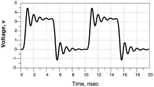
Figure 8-1. “Ringing” noise at the receiver end of a 1-inch-long controlled-impedance interconnect created because of impedance mismatches and multiple reflections at the ends of the line.
Reflections occur whenever the instantaneous impedance the signal sees changes. This can be at the ends of lines or wherever the topology of the line changes, such as at corners, vias, tees, connectors, and packages. By understanding the origin of these reflections and arming ourselves with the tools to predict their magnitude, we can engineer a design with acceptable system performance.
TIP
For optimal signal quality, the goal in interconnect design is to keep the instantaneous impedance the signal sees as constant as possible.
First, this means keeping the characteristic impedance of the line constant. Hence, the growing importance in manufacturing controlled-impedance boards. All the other tricks, such as minimizing stub lengths, using daisy chains rather than branches, and using point-to-point topology, are all methods to keep the instantaneous impedance constant.
Second, this means managing impedance changes with topology design and adding discrete resistors to maintain a constant instantaneous impedance for the signal.
As a signal propagates down a transmission line, it sees an instantaneous impedance for each step along the way. If the interconnect is a controlled impedance, then the instantaneous impedance will be equal to the characteristic impedance of the line. If the instantaneous impedance should ever change, for whatever reason, some of the signal will reflect back in the opposite direction and some of it will continue with a different amplitude. We call all locations where the instantaneous impedance changes impedance discontinuities or just discontinuities.
The amount of signal that reflects depends on the magnitude of the change in the instantaneous impedance. This is illustrated in Figure 8-2. If the instantaneous impedance in the first region is Z1 and the instantaneous impedance in the second region is Z2, the magnitude of the reflected signal compared to the incident signal will be given by:
where:
V reflected = the reflected voltage
Vincident = the incident voltage
Z1 = the instantaneous impedance of the region where the signal is initially
Z2 = the instantaneous impedance of the section where the signal just enters
ρ = the reflection coefficient, in units of rho

Figure 8-2. Whenever a signal sees a change in the instantaneous impedance, there will be some reflected signal, and the transmitted signal will be distorted.
The greater the difference in the impedances in the two regions, the greater the amount of reflected signal. For example, if a 1-v signal is moving on a 50-Ohm characteristic-impedance transmission line, it will see an instantaneous impedance of 50 Ohms. If it hits a region where the instantaneous impedance changes to 75 Ohms, the reflection coefficient will be (75 – 50)/(75 + 50) = 20%, and the amount of reflected voltage will be 20% × 1 v = 0.2 v.
For every part of the waveform that hits the interface, exactly 20% of it will reflect back. This is true no matter the shape of the waveform. In the time domain, it can be a sharp edge, a sloping edge, or even a Gaussian edge. Likewise, in the frequency domain, where all waveforms are sine waves, each sine wave will reflect and the amplitude and phase of the reflected wave can be calculated from this relationship.
It is often the reflection coefficient, ρ (or rho), that is of interest. The reflection coefficient is the ratio of the reflected voltage to the incident voltage.
TIP
The most important thing to remember about the reflection coefficient is that it is equal to the ratio of the second impedance minus the first, divided by their sum. This distinction is particularly important in determining the sign of the reflection coefficient.
When considering signals on interconnects, keeping track of their direction of travel on the interconnect is critically important. If a signal is traveling down a transmission line and hits a discontinuity, a second wave will be generated at the discontinuity. This second wave will be superimposed on the first wave, but will be traveling back toward the source. The amplitude of this second wave will be the incident voltage times rho.
The reflection coefficient describes the fraction of the voltage that reflects back to the source. In addition, there is a transmission coefficient that describes the fraction of the incident voltage that is transmitted through the interface into the second region. This property of signals to reflect whenever the instantaneous impedance changes is the source of all signal-quality problems related to signal propagation on one net.
To minimize signal-integrity problems that arise because of this fundamental property, we must implement the following four important design features for all high-speed circuit boards:
Use controlled impedance interconnects.
Provide at least one termination at the ends of a transmission line.
Use a routing topology that minimizes the impact from multiple branches.
Minimize any geometry discontinuities.
But what causes the reflection? Why does a signal reflect when there is a change in the instantaneous impedance it sees? The reflected signal is created to match two important boundary conditions.
Consider the interface between two regions, labeled as region 1 and region 2, each with a different instantaneous impedance. As the signal hits the interface, we must see only one voltage between the signal- and return-path conductors and one current loop flowing between the signal- and return-path conductors. Whether we look from the region 1 side or change our perspective and look from the region 2 side, we must see the same voltage and the same current on either side of the interface. We must not have a voltage discontinuity across the boundary, because this would mean an infinitely large electric field in the boundary. We must not have a current discontinuity, as this would mean an infinitely large magnetic field in the boundary.
Without the creation of a reflected voltage heading back to the source and while maintaining the same voltage and current across the interface, we would have the condition of V1 = V2 and I1 = I2. But, I1 = V1/Z1 and I2 = V2/Z2. If the impedances of the two regions are not the same, there is no way all four conditions can be met.
To keep harmony in the universe, a new voltage is created in the first region that reflects back to its source. Its sole purpose is to take up the mismatched current and voltage between the incident and transmitted signals. Figure 8-3 illustrates what happens at the interface.

Figure 8-3. As the incident signal tries to pass through the interface, a reflected voltage and current are created to match the voltage and current loops on both sides of the interface.
The incident voltage, Vinc, moves toward the interface, while the transmitted voltage, Vtrans, moves away from the interface. A new voltage is created as the incident signal tries to pass through the interface. This new wave is traveling only in region 1, back to the source.
The condition of the same voltages on both sides of the interface requires:
The condition on the currents is a little more subtle. The total current at the interface, in region 1, is due to two current loops, each traveling in opposite directions and circulating in opposite directions. At the interface, the direction of the incident current loop is clockwise. The direction of the reflected current loop is counterclockwise. If we define the positive direction as clockwise, then the net current at the interface in region 1 is Iinc – Irefl. In region 2, the current loop is clockwise and is just Itrans. The condition of the same current viewed from either side of the interface is:
The final condition is that the ratio of voltage to the current in each region is the impedance of each region:
Using these last relationships, we can rewrite the condition of the current as:
With a little bit of algebra, we get:
and
and finally,
which is the definition of the reflection coefficient. Using the same approach, we can derive the transmission coefficient as:
Dynamically, what actually creates the reflected voltage? No one knows. We only know that if it is created, we are able to match the same voltage on one side of the interface with that on the other side. The voltage is continuous over the interface. Likewise, the current loop is exactly the same on both sides of the interface. The current is continuous across the interface. The universe is in balance.
There are three important special cases to consider for transmission line terminations. In each case, the transmission line characteristic impedance is 50 Ohms. The signal will be traveling in this transmission line from the source and hit the far end with a particular termination.
When the second impedance is an open, as is the case when the signal hits the end of a transmission line with no termination, the instantaneous impedance at the end is infinite. The reflection coefficient is (infinite – 50)/(infinite + 50) = 1.
TIP
It is important to keep in mind that in the time domain, the signal is sensitive to an instantaneous impedance. It is not necessary that the second region be a transmission line. It might also be a discrete device that has some impedance associated with it, such as a resistor, capacitor, inductor, or some combination thereof.
This means a second wave of equal size to the incident wave will be generated at the open but will be traveling in the opposite direction—back to the source.
If we look at the total voltage appearing at the far end, where the open is, we will see the superposition of two waves. One, with an amplitude of 1 v, will be traveling toward the open end. The other, also with an amplitude of 1 v, will be traveling in the opposite direction. When we measure the voltage at the far end, we measure the sum of these two voltages, or 2 v. This is illustrated in Figure 8-4.
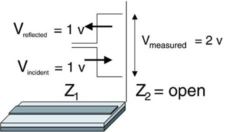
Figure 8-4. If the second impedance is an open, the reflection coefficient is 1. At the open, there will be two oppositely traveling waves superimposed.
TIP
It is often said that when a signal hits the end of a transmission line, it doubles. While this is technically true, it is not what is really happening. The total voltage, the sum of the two traveling waves, is twice the incident voltage. However, if we think of it as a doubling, we misscalibrate our intuition. It is better to think of the voltage at the far end as the sum of the incident and the reflected voltage.
The second special case is when the far end of the line is shorted to the return path. The impedance at the end is 0 in this case. The reflection coefficient is (0 – 50)/(0 + 50) = –1. When a 1-v signal is incident to the far end, a –1-v signal is generated by the reflection. This second wave propagates back through the transmission line to the source.
The voltage that would be measured at the shorting discontinuity is the sum of the incident voltage and the reflected voltage, or 1 v + –1 v = 0. This is reasonable, because if we really have a short at the far end, by definition, we can't have a voltage across a short. We see now that the reason it is 0 v is that it is the sum of two waveforms, a positive one traveling in the direction from the source and a negative one traveling back toward it.
The third important impedance at the far end to consider is when the impedance matches the characteristic impedance of the transmission line. In this example, it could be created by adding a 50-Ohm resistor to the end. The reflection coefficient would be (50 – 50)/(50 + 50) = 0. There would be no reflected voltage from the end. The voltage appearing across the 50-Ohm termination resistor would just be the incident-voltage wave.
If the instantaneous impedance the signal sees does not change, there will be no reflection. By placing the 50-Ohm resistor at the far end, we have matched the termination impedance to the characteristic impedance of the line and reduced the reflection to zero.
For any resistive load at the far end, the instantaneous impedance the signal will see will be between 0 and infinity. Likewise, the reflection coefficient will be between –1 and +1. Figure 8-5 shows the relationship between terminating resistance and reflection coefficient for a 50-Ohm transmission line.
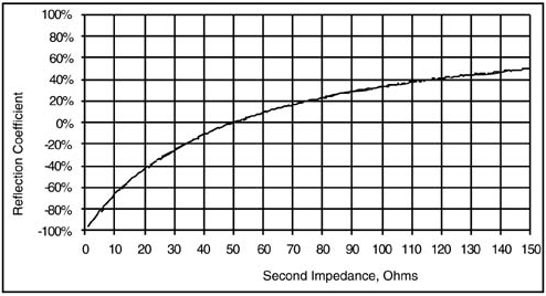
Figure 8-5. Reflection coefficient for the case of the first impedance being 50 Ohms and a variable impedance for the second region.
When the second impedance is less than the first impedance, the reflection coefficient is negative. The reflected voltage from the termination will be a negative voltage. This negative-voltage wave propagates back to the source.
TIP
When the second impedance is less than the first impedance, the voltage appearing across the resistor will always be less than the incident voltage.
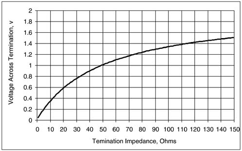
For example, if the transmission line characteristic impedance is 50 Ohms and the termination is 25 Ohms, the reflection coefficient is (25 – 50)/(25 + 50) = –1/3. If 1 v were incident to the termination, a –0.33 v will reflect back to the source. The actual voltage that would appear at the termination is the sum of these two waves, or 1 v + –0.33 v = 0. 67 v.
Figure 8-6 shows the measured voltage that would appear across the termination for a 1-v incident voltage and a 50-Ohm transmission line. As the termination impedance increases from 0 Ohms, the actual voltage measured across the termination increases from 0 v up to 2 v when the termination is open.
When a signal is launched into a transmission line, there is always some impedance of the source. For typical CMOS devices, this can be about 5 Ohms to 20 Ohms. For older-generation transistor transistor logic (TTL) gates, this can be as high as 100 Ohms. The source impedance will have a dramatic impact on both the initial voltage launched into the transmission line and the multiple reflections. When the reflected wave finally reaches the source, it will see the output-source resistance as the instantaneous impedance right at the driver. The value of this output-source impedance will determine how the reflected wave reflects again from the driver.
If we have a model for the driver, either SPICE or IBIS based, a good estimate of the output impedance of the driver can be extracted with a few simple simulations. We assume an equivalent circuit model for the driver is an ideal voltage source in series with a source resistor, illustrated in Figure 8-7. We can extract the output voltage of the ideal source when driving a high-output impedance. If we connect a low impedance like 10 Ohms to the output, and measure the output voltage across this terminating resistor, we can back out the internal-source resistance from:
where:
Rs = the source resistance of the driver
Rt = the terminating resistance connected to the output
Vo = the open-circuit output voltage from the driver
Vt = the voltage across the terminating resistor

To calculate the source resistance, we simulate the output voltage from the driver in two cases: when a very high resistance is attached (e.g., 10 kOhms) and when a low impedance is attached (e.g., 10 Ohms). An example of the simulated voltage using a behavioral model for a common CMOS driver, is shown in Figure 8-8. The open-circuit voltage is 3.3 v, and the voltage with the 10-Ohm resistor attached is 1.9 v. From the equation above, the output-source impedance can be calculated as 10 Ohms × (3.3 v/1.9 v – 1) = 7.3 Ohms.
As shown in the previous chapter, the actual voltage launched into the transmission line, or the incident voltage to the transmission line, is determined by the combination of the source voltage and the voltage divider made up of the source impedance and the transmission line.
Knowing the time delay of the transmission lines, TD, and the impedances of each region where the signal will propagate, and knowing the initial voltage from the driver, we can calculate all the reflections at all the interfaces and predict the voltages that would be measured at any point in time.
For example, if the source voltage, driving an open termination, were 1 v and the source impedance were 10 Ohms, the actual voltage launched into a 1-nsec-long, 50-Ohm transmission line would be 1 v × 50/(10 + 50) = 0.84 v. This 0.84-v signal would be the initial incident voltage propagating down the transmission line.
Suppose the end of the transmission line was an open termination. The 0.84-v signal would hit the end of the line 1 nsec later and a +0.84-v signal would be generated by the reflection, traveling back to the source. At the end of the line, the total voltage measured across the open will be the sum of the two waves, or 0.84 v + 0.84 v = 1.68 v.
When the 0.84-v reflected wave hits the source end, another 1 nsec later, it will see an impedance discontinuity. The reflection coefficient at the source is (10 – 50)/(10 + 50) = –0.67. With a 0.84-v signal incident on the interface, a total of 0.84 v × –0.67 = –0.56 v will reflect back to the end of the line. Of course, this new wave will reflect again from the far end. A step voltage change of –0.56 v will reflect back. Measured at the far end, across the open, will be four simultaneous waves: 2 × 0.84 v or 1.68 v from the first wave, and 2 × –0.56 v or –1.12 v from the second reflection for a total voltage of 0.56 v.
The –0.56-v wave will hit the source impedance and reflect yet again. The reflected voltage will be +0.37 v. At the far end, there will be the 0.56 v from the first two waves plus the new set of incident and reflected 0.37-v waves, for a total of 0.56 v + 0.37 v + 0.37 v = 1.3 v. Keeping track of these multiple reflections is straightforward but tedious. Before the days of simple, easy-to-use simulation tools, these reflections were diagramed using “bounce” or “lattice” diagrams. An example is shown in Figure 8-9.

Figure 8-9. Lattice or bounce diagram used to keep track of all the multiple reflections and the time-varying voltages at the receiver on the far end.
When the source impedance is less than the characteristic impedance of the transmission line, we see that the reflection at the source end will be negative. This will contribute to the effect we normally call ringing. Figure 8-10 shows the voltage waveform at the far end of the transmission line for the previous example, when the rise time of the signal is very short compared to the time delay of the transmission line. This analysis was done using a SPICE simulator to predict the waveforms at the far end, taking into account all the multiple reflections and impedance discontinuities.

Figure 8-10. Simulated voltage at the far end of the transmission line described with the previous lattice diagram. Simulation performed with SPICE.
Two important features should be apparent. First, the voltage at the far end eventually approaches the source voltage, or 1 v. This must be the case, because we have an open and we must ultimately see the source voltage across an open.
The second important effect is that the actual voltage across the open exceeds the voltage coming out of the source. The source has only 1 v, yet we would measure as much as 1.68 v at the far end. How was this higher voltage generated? The higher voltage is really generated by the resonance of the distributed L and C of the transmission line.
Using the definition of the reflection coefficient above, the reflected signal from any arbitrary impedance can be calculated. When the terminating impedance is a resistive element, the impedance is constant and the reflected voltages are easy to calculate. When the termination has a more complicated impedance behavior (such as a capacitive or inductive termination, or some combination of the two), calculating the reflection coefficient and how it changes as the incident waveform changes is difficult and tedious if done by hand. Luckily, there are simple, easy-to-use circuit-simulation tools that make this calculation much easier.
The reflection coefficients and the resulting reflected waveforms from arbitrary impedances and for arbitrary waveforms can be calculated using either SPICE circuit simulators or behavioral simulators. With both tools, sources are created, ideal transmission lines are added, and terminations are connected. The voltage appearing across the termination and any other nodes can be calculated as the incident waveform hits the end and reflects from all the various discontinuities.
There are many possible combinations of source impedance, transmission line characteristic impedance, time delay, and end termination. Each of these can be easily varied using a simulation tool. Figure 8-11 shows the simulated voltage across the termination as the rise time of the signal is increased from a 0.1 nsec to 1 nsec and, in a separate simulation, the signal waveform as the source terminating resistance is varied from 0 Ohms to 90 Ohms.
Figure 8-11. Examples of the variety of simulations possible with SPICE. Top: for a 10-Ohm driver and 50-Ohm characteristic-impedance line, showing the far-end voltage with different rise times for the signal. Bottom: changing the series-source terminating resistor and displaying the voltage at the far end.
In addition to simulating the waveforms associated with transmission line circuits, it is possible to measure the reflected waveforms from physical interconnects using a specialized instrument usually referred to as a time domain reflectometer, or a TDR. This is the appropriate instrument to use when characterizing a passive interconnect that does not have its own voltage source. Of course, when measuring the actual voltages in an active circuit, a fast oscilloscope with a high-impedance probe is the best tool.
A TDR will generate a short rise-time step edge, typically between 35 psec and 150 psec, and measure the voltage at an internal point of the instrument. Figure 8-12 is a schematic of the workings inside a TDR. It is important to keep in mind that a TDR is nothing more than a fast step generator and a very fast sampling scope.
Figure 8-12. Schematic of the inside of a TDR. A very fast pulse generator creates a fast rising-voltage pulse. It travels through a precision 50-Ohm resistor in series with a short length of 50-Ohm coax cable to the front panel where the DUT is connected. The total voltage at an internal point is measured with a very fast sampling oscilloscope and displayed on the front screen.
The voltage source is a very fast step generator, which outputs a step amplitude of about 400 mV. Right after the voltage source is a calibrated resistor of 50 Ohms. This assures that the source impedance of the TDR is a precision 50 Ohms. After the resistor is the actual detection point where the voltage is measured by a fast sampling amplifier. Connected to this point is a short-length coax cable that brings the signal to the front-panel SMA connector. This is where the DUT is connected. The signal from the source enters the DUT and any reflected voltage is detected at the sampling point.
Before the step signal is generated, the voltage measured at the internal point will be 0 v. Where the voltage is actually measured, the signal encounters a voltage divider. The first resistor is the internal calibration resistor. The second resistor is the transmission line internal to the TDR. As the 400-mV step reaches the calibration resistor, the actual voltage measured at the detection point will be the result after going through the voltage divider.
The voltage detected is 400 mV × 50 Ohms/(50 Ohms + 50 Ohms) = 200 mV. This voltage is measured initially and is displayed by the fast sampling scope. The 200-mV signal continues moving down the internal coax cable to the DUT.
If the DUT is a 50-Ohm termination, there is no reflected signal and the only voltage present at the sampling point is the forward-traveling wave of 200 mV, which is constant. If the DUT is an open, the reflected signal from the DUT is +200 mV. A short time after launch, this 200-mV reflected-wave signal comes back to the sampling point, and what is measured and displayed is the 200-mV incident voltage + the 200-mV reflected wave. The total voltage displayed is 400 mV.
If the DUT is a short, the reflected signal from the DUT will be –200 mV. Initially, the 200-mV incident voltage is measured. After a short time, the reflected –200-mV signal comes back to the source and is measured by the sampling head. What is measured at this point is the 200-mV incident plus the –200-mV reflected signal, or 0 voltage. The measured-TDR plots of these cases are shown in Figure 8-13.
Figure 8-13. Measured-TDR response when the DUT is an open and a short. Data measured with an Agilent 86100 DCA and displayed with TDA Systems IConnect software.
TIP
The TDR will measure the reflected voltage from any interconnect attached to the front SMA connector of the instrument and how this voltage changes with time as the signal propagates down the interconnect, reflecting from all discontinuities.
As the transmitted signal continues down the DUT, if there are other regions where the instantaneous impedance changes, a new reflected voltage will be generated and will travel back to the internal measurement point to be displayed. In this sense, the TDR is really indicating changes in the instantaneous impedance the signal encounters and when the signal encounters it.
Since the incident signal must travel down the interconnect and the reflected signal must travel back down the interconnect to the detection point, the time delay measured on the front screen is really a round-trip delay to any discontinuity.
For example, if a uniform 4-inch-long, 50-Ohm transmission line is the DUT, we will see an initial small reflected voltage at the entrance to the DUT because it is not exactly 50 Ohms, and then a larger reflected signal when the incident signal reaches the open at the far end and reflects back to the detection point. This time delay is the round-trip time delay of the transmission line. If the transmission line is not 50 Ohms, then multiple reflections will take place at both ends of the line. The TDR will display the superposition of all the voltage waves that make it back to the internal measurement point. An example of the TDR response from a 50-Ohm transmission line and a 15-Ohm transmission line, both open at the far end, is shown in Figure 8-14.
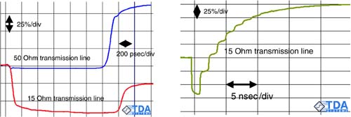
Figure 8-14. Measured TDR response of 4-inch-long transmission lines open at the far end: 50 Ohms and 15 Ohms. Left: time base of 200 psec/div. Right: reflections from the 15-Ohm line on expanded time base, 5 nsec/div. Measured with Agilent 86100 DCA and a GigaTest Labs Probe Station and displayed with TDA Systems IConnect.
The combination of understanding the principles and leveraging simulation and measurement tools will allow us to evaluate many of the important impedance discontinuities a signal might encounter. We will see that many of them are important and must be carefully engineered or avoided, while some of them are not important and can be ignored in some cases.
Wherever a signal sees an impedance change, there will be a reflection. Reflections can have a serious impact on signal quality. Predicting the impact on the signals from the discontinuities and engineering acceptable design alternatives is an important part of signal-integrity engineering.
Even if a circuit board is designed with controlled-impedance interconnects, there is still the opportunity for a signal to see an impedance discontinuity from such features as:
The ends of the line
A package lead
An input-gate capacitance
A via between signal layers
A corner
A stub
A branch
A test pad
A gap in the return path
A neck down in a via field
A crossover
When we model these effects, there are three common equivalent-circuit models we can use to electrically describe the unintentional discontinuity: an ideal capacitor, an ideal inductor, or a short-length ideal transmission line (either in series or in shunt). These possible equivalent circuit models are shown in Figure 8-15. These circuit elements can occur at the ends of the line or in the middle.
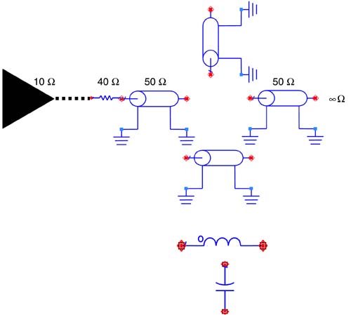
Figure 8-15. Transmission line circuit used to illustrate the specific impedance from the three types of discontinuities, short transmission line in series and shunt, shunt capacitive, and series inductive.
The two most important parameters that influence the distortion of the signal from the discontinuity are the rise time of the signal and how large the discontinuity is. For an inductor and capacitor, their instantaneous impedance depends on the instantaneous rate at which either the current is changing or the voltage is changing. As the signal passes across the element, the slope of the current and the voltage will change with time and the impedance of the element will change in time. This means the reflection coefficient will change with time and with the specific features of the rise or fall time. The peak reflected voltage will scale with the rise time of the signal.
In general, the impact of a discontinuity is further complicated by the impedance of the driver and the characteristic impedance of the initial transmission line influencing the multiple bounces.
Any impedance discontinuity will cause some reflection and distortion of the signal. It is not impossible to design an interconnect with absolutely no reflections. How much noise can we live with and how much noise is too much? This depends very strongly on the noise budget and how much noise voltage has been allocated to each source of noise.
TIP
These factors as well as the impact from the discontinuity itself can only be fully taken into account by converting the physical structure that creates the discontinuity into its equivalent electrical-circuit model and performing a simulation. Rule-of-thumb estimates can only provide engineering insight and offer rough guidelines for when a problem might arise.
TIP
Unless otherwise specified, as a rough rule of thumb, the reflection noise level should be kept to less than 10% of the voltage swing. For a 3.3-v signal, this is 330 mV of noise. Some noise budgets might be more conservative and allocate no more than 5% to reflection noise. The tighter the noise budget, typically, the more expensive the solution. Often, the noise allocated to one source may be tightened up because the fix to correct it is less expensive to implement, while another might be loosened because it is more expensive to fix. As a rough rule of thumb, we should definitely worry about the reflection noise if it approaches or exceeds 10% of the signal swing. In some designs, less than 5% may be too much.
By evaluating a few simple cases, we can see what physical factors influence the signal distortions and how to engineer them out of the design before they become problems. Ultimately, the final evaluation of whether a design is acceptable or not must come from a simulation. This is why it is so important that every practicing engineer with a concern about signal integrity have easy access to a simulator to be able to evaluate specific cases.
The simplest transmission line circuit has a driver at one end, a short length of controlled-impedance line, and a receiver at the far end. As we saw previously, the signal will bounce around between the high-impedance open at the far end and the low impedance of the driver at the near end. When the length of the line is long, these multiple bounces will cause signal-quality problems, which we lump in the general category of ringing. But if the line is short enough, though the reflections will still happen, they may be smeared out with the rising or falling edge and may not pose a problem. Figure 8-16 illustrates the received waveform as the time delay, TD, of the 50-Ohm transmission line is changed from 20% of the rise time, 30% of the rise time, and 40% of the rise time.
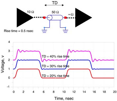
Figure 8-16. 100-MHz clock signal at the far end of an unterminated transmission line as its length is changed from 20% of the rise time, to 30% and 40% of the rise time. When the time delay of the transmission line is greater than 20% of the rise time, ringing noise may cause a problem.
When the TD of the interconnect is 0.1 nsec long, all the reflections take place but they rattle around back and forth every 0.2 nsec, the round-trip time of flight. If this is short compared with the rise time, the multiple bounces will be smeared over the rise time and will be barely discernible, not posing a potential problem. In the previous figure, as a rough estimate, it appears that when the TD is less than 20%, the reflections are virtually invisible, but if the TD is greater than 20% of the rise time, the ringing begins to play a significant role.
TIP
We use, as a rough rule of thumb, the threshold of TD > 20% of the rise time as the boundary of when to start worrying about ringing noise due to an unterminated line. If the TD of the transmission line is greater than 20% of the rise time, ringing will play a role and must be managed, otherwise it will potentially cause a signal-integrity problem. If the TD < 20% of the rise time, the ringing noise may not be a problem and the line may not require termination.
For example, if the rise time is 1 nsec, the maximum TD for a transmission line that might be used unterminated is ~ 20% × 1 nsec = 0.2 nsec. In FR4, the speed of a signal is about 6 inches/nsec, so the maximum physical length of an unterminated line is roughly 6 inches/nsec × 0.2 nsec = 1.2 inches.
This allows us to generalize a very useful rule of thumb that the maximum length for an unterminated line before signal-integrity problems arise is roughly:
where:
Lenmax = the maximum length for an unterminated line, in inches
RT = the rise time, in nsec
TIP
This is a very useful and easy to remember result. As a rough rule of thumb, the maximum length of an unterminated line (in inches) is the rise time (in nsec).
If the rise time is 1 nsec, the maximum unterminated length is about 1 inch. If the rise time is 0.1 nsec, the maximum unterminated length is 0.1 inch. As we shall see, this is the most important general rule of thumb to identify when ringing noise will play a significant role. This is also why signal integrity is becoming a significant problem in recent years and might have been avoided in older generation technologies.
When clock frequencies were 10 MHz, the clock periods were 100 nsec and the rise times were about 10 nsec. The maximum unterminated line would be 10 inches. This is longer than virtually all traces on a typical mother board. Back in the days of 10-MHz clocks, though the interconnects always behaved like transmission lines, the reflection noise never caused a problem and the interconnects were “transparent” to the signals. We never had to worry about impedance matching, terminations, or transmission line effects.
However, the form factor of products is staying the same, and lengths of interconnects are staying fixed, but rise times are decreasing. Therefore, it is inevitable that we reach a high enough clock frequency with a short enough rise time that virtually all the interconnects on a board will be longer than the maximum possible unterminated length and termination will be important.
These days, with rise times of signals as short as 0.25 nsec, the maximum unterminated length of a transmission line before ringing noise becomes important is about 0.25 inch. Virtually 100% of all interconnects are longer than this. A termination strategy is a must in all of today's and future-generation's products.
We have identified the origin of the ringing as the impedance discontinuities at the source and the far end and the multiple reflections back and forth. If we eliminate the reflections from at least one end, we can minimize the ringing.
TIP
Engineering the impedance at one or both ends of a transmission line to minimize reflections is called terminating the line. Typically one or more resistors are added at strategic locations.
When one driver drives one receiver, we call this a point-to-point topology. There are four techniques to terminate a point-to-point topology illustrated in Figure 8-17. The most common method is using a resistor in series at the driver. This is called source-series termination. The sum of the terminating resistor and the source impedance of the driver should add up to the characteristic impedance of the line.
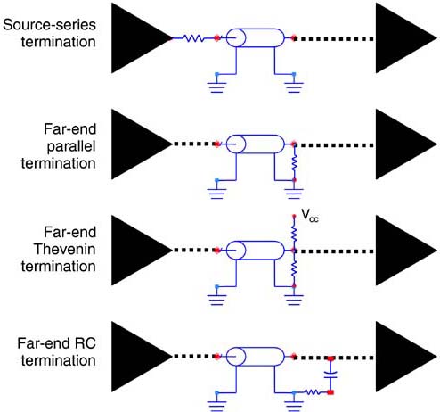
Figure 8-17. Four common termination schemes for point-to-point topologies. The top one, source-series termination, is the most commonly used approach.
If the driver-source impedance is 10 Ohms and the characteristic impedance of the line is 50 Ohms, then the terminating resistor should be about 40 Ohms. With this terminating resistor in place, the 1-v signal coming out of the driver will now encounter a voltage divider composed of the 50-Ohm total resistance and the 50-Ohm transmission line. In this case, 0.5 v will be launched into the transmission line.
At first glance, it might seem that half the source voltage will not be enough to affect any triggering. However, when this 0.5-v signal hits the open end of the transmission line, it will again see an impedance discontinuity. The reflection coefficient at the open is 1, and the 0.5-v incident signal will reflect back to the source with an amplitude of 0.5 v. At the far end, the total voltage across the open termination will be the 0.5-v incident voltage and the 0.5-v reflected voltage, or a total of 1 v.
The 0.5-v reflected signal travels back to the source. When it reaches the series terminating resistance, the impedance it sees looking into the source is the 40 Ohms of the added series resistor plus the 10 Ohms of the source, or 50 Ohms. It is already in a 50-Ohm transmission line; therefore the signal will encounter no impedance change and there will be no reflection. The signal will merely be absorbed by the terminating resistor and the source resistor.
At the far end, all that is seen is a 1-v signal and no reflections. Figure 8-18 shows the waveform at the far end for the case of no terminating resistor and the 40-Ohm source-series terminating resistor.
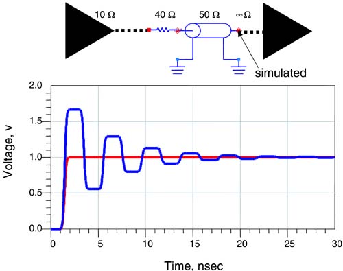
Figure 8-18. Voltage signal of a fast edge, at the far end of the transmission line with and without the source series terminating resistor.
TIP
Understanding the origin of the reflections allows us to engineer a solution to eliminate reflections at one end and prevent ringing. The resulting waveform is very clean and free of signal-quality problems.
At the near end, coming out of the source, right after the source-series terminating resistor, the initial voltage that would be measured is just the incident voltage launched into the transmission line. This is about half the signal voltage. Looking at the source end, we would have to wait for the reflected wave to come by to bring the total voltage up to the full voltage swing. For a time equal to the round-trip time of flight, the voltage at the source end, after the series resistor, will encounter a shelf. The longer the round-trip time delay of the transmission line compared to the rise time, the longer the shelf will last. This is a fundamental characteristic of source-series terminated lines. An example of the measured voltage at the source end is shown in Figure 8-19.

Figure 8-19. 100-MHz clock signal, measured at the source end of the transmission line with a source-series resistor as the length of the line is increased. Rise time of the signal is 0.5 nsec.
As long as there are no other receivers near the source to see this shelf, it will not cause a problem. It is when other devices are connected near the source, that the shelf may cause a problem and other topologies and termination schemes might be required.
In the following examples, we are always assuming the source impedance has been matched to the 50-Ohm characteristic impedance of the initial transmission line.
Many times the line width of a trace on a board must neck down, as it might in going through a via field or routing around a congested region of the board. If the line width changes for a short length of the line, the characteristic impedance will change, typically increasing. How much change in impedance and over what length might start to cause a problem?
There are three features that determine the impact from a short transmission line segment: the time delay (TD) of the discontinuity, the characteristic impedance of the discontinuity (Z0), and the rise time of the signal (RT). When the time delay is long compared to the rise time, in other words, the discontinuity is electrically long, the reflection coefficient will saturate. The maximum value of the reflection coefficient will be related to the reflection from the front of the discontinuity:
For example, if the neck down causes an impedance change from 50 Ohms to 75 Ohms, the reflection coefficient would be 0.2. Some examples of the reflected and transmitted signals from electrically long transmission line discontinuities are shown in Figure 8-20.
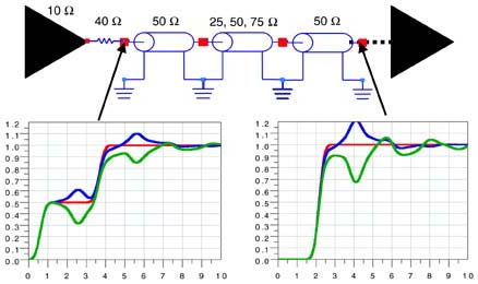
Figure 8-20. Reflected and transmitted signal in a transmission line circuit with an electrically long but uniform discontinuity, as the impedance of the discontinuity is changed.
These impedance discontinuities cause the signal to rattle around, contributing to reflection noise. This is why it is so important to design interconnects with one, uniform characteristic impedance. To keep the reflection noise to less than 5% of the voltage swing requires keeping the characteristic-impedance change to less than 10%. This is why the typical spec for the control of the impedance in a board is for +/– 10%.
Note that whatever the reflection is from the first interface, it will be equal but of opposite sign from the second interface, since Z1 and Z2 would be reversed. If the discontinuity can be kept short, the reflections from the two ends might cancel and the impact on signal quality can be kept negligible. Figure 8-21 shows the reflected and transmitted signal with a short-length discontinuity that is 25 Ohms. If the TD of the discontinuity is shorter than 20% the rise time, the discontinuity may not cause problems. This gives rise to the same general rule of thumb as before; that is, the maximum acceptable length for an impedance discontinuity is:
where:
Lenmax = the maximum length for a discontinuity, in inches
RT = the rise time, in nsec

Figure 8-21. Reflected and transmitted signal in a transmission line circuit with an electrically short but uniform discontinuity, as the time delay of the discontinuity is increased from 0% to 40% of the rise time.
TIP
If the TD of the discontinuity can be kept shorter than 20% of the rise time, the impact from the discontinuity may be negligible. This is the same rule of thumb that the length of the discontinuity, in inches, should be less than the rise time of the signal, in nsec.
For example, if the rise time is 0.5 nsec, neck downs shorter than 0.5 inch may not cause a problem.
Often, a branch is added to a uniform transmission line to allow the signal to reach multiple fan outs. When the branch is short, it is called a stub. A stub is commonly found on BGA packages to allow bussing all the pins together so the bonding pads can be gold plated. The busses are broken off during manufacturing, leaving small, short-length stubs attached to each signal line.
The impact from a stub is complicated to analyze because of all the many reflections that must be taken into account. As the signal leaves the driver, it will first encounter the branch point. Here it will see a low impedance from the parallel combination of the two transmission line segments, and a negative reflection will head back to the source. A fraction of the signal will continue down both branches. When the signal in the stub hits the end of the stub, it will reflect back to the branch point, again reflecting back to the end and rattling around in the stub. At the same time, at each interaction with the branch point, some fraction of the signal in the stub will head back to the source and to the far end. Each interface acts as a point of reflection.
The only practical way of evaluating the impact of a stub on signal quality is by using a SPICE or a behavioral simulator. The two important factors that determine the impact of the stub on signal quality are the rise time of the signal and the length of the stub. In this example, we assume the stub is located in the middle of the transmission line and has the same characteristic impedance as the main line. Figure 8-22 shows the simulated reflected signal and transmitted signal as the stub length is increased from 20% of the rise time to 60% of the rise time.

Figure 8-22. Reflected and transmitted signal in a transmission line circuit with a short stub in the middle, while the time delay of the stub is increased from 20% to 60% of the rise time.
TIP
As a rough rule of thumb, if the stub length is kept shorter than 20% of the spatial extent of the rise time, the impact from the stub may not be important. Likewise, if the stub is longer than 20% of the rise time, it may have an important impact on the signal and must be simulated to evaluate whether it will be acceptable.
For example, if the rise time of the driver is 1 nsec, a stub with a time delay shorter than 0.2 nsec might be acceptable. The length of the stub would be about 1 inch. Once again, the rule of thumb is:
where:
Lstubmax = the maximum acceptable stub length, in inches
RT = the signal rise time, in nsec
This is a simple, easy-to-remember rule of thumb. For example, for a 1-nsec rise time, keep stubs shorter than 1 inch. If the rise time is 0.5 nsec, keep stubs shorter than 0.5 inch. It is clear that as rise times decrease, it gets harder and harder to engineer stubs short enough to not impact signal integrity.
In BGA packages, it is often not possible to avoid plating stubs used in the manufacture of the packages. These stubs are typically less than 0.25 inch long. When the rise time of the signals is longer than 0.25 nsec, these plating stubs may not cause a problem, but as rise times drop below 0.25 nsec, they definitely will cause problems and it may be necessary to pay extra for packages that are manufactured without plating stubs.
All real receivers have some input-gate capacitance. This is typically on the order of 2 pF. In addition, the receiver's package-signal lead might have a capacitance to the return path of about 1 pF. If there is a bank of three memory devices at the end of a transmission line, there might be as much as a 10-pF load at the end of the transmission line.
When a signal travels down a transmission line and hits an ideal capacitor at the end, the actual instantaneous impedance the signal sees, which determines the reflection coefficient, will change with time. After all, the impedance of a capacitance, in the time domain, is related to:
where:
Z = the instantaneous impedance of the capacitor
C = the capacitance of the capacitor
V = the instantaneous voltage in the signal
If the rise time is short compared with the charging time of the capacitor, then initially, the voltage will rise up very fast and the impedance will be low. But as the capacitor charges, the voltage across it gets smaller and the dV/dt slows down. As the capacitor charges up, the rate at which the voltage across it changes will slow down. This will cause the impedance of the capacitor to increase dramatically. If we wait long enough, the impedance of a capacitor, after it has charged fully, is open.
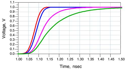
This means the reflection coefficient will change with time. The reflected signal should suffer a dip and then move up to look like an open. The exact behavior will depend on the characteristic impedance of the line (Z0), the capacitance of the capacitor, and the rise time of the signal. The simulated reflected and transmitted voltage behavior for a 2-pF, 5-pF, and 10-pF capacitance is shown in Figure 8-23.
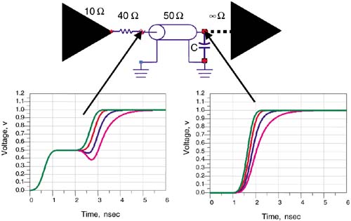
Figure 8-23. Reflected and transmitted signal in a transmission line circuit with a capacitive load at the far end, for a 0.5-nsec rise time and capacitances of 0, 2 pF, 5 pF, and 10 pF.
The long-term response of the transmitted voltage pattern looks like the charging of a capacitor by a resistor. The presence of the capacitor filters the rise time and acts as a “delay adder” for the signal at the receiver. We can estimate the new rise time and the increase in time delay for the signal to transition through the midpoint (i.e., the delay adder), because it is very similar to the charging of an RC circuit, where the voltage increases with an exponential time constant:
This time constant is how long it takes for the voltage to rise up to 1/e or 37% of the final voltage. The 10%–90% rise time is related to the RC time constant by:
At the end of a transmission line with a capacitive load, it looks like the voltage is charging up with an RC behavior. The C is the capacitance of the load. The R is the characteristic impedance of the transmission line, Z0. The 10–90 rise time for the transmitted signal, if dominated by the RC charging, is roughly:
For example, if the transmission line has a characteristic impedance of 50 Ohms and the capacitance is 10 pF, the 10–90 charging time will be 2.2 × 50 Ohms × 10 pF = 1.1 nsec. If the initial-signal rise time is short compared with this 1.1-nsec charging time, the presence of the capacitive load at the end of the line will dominate and will now determine the rise time at the receiver. If the initial rise time of the signal is long compared to the 10–90 charging rise time, the capacitor at the end will add a delay to the rise time, roughly equal to the 10–90 rise time.
TIP
Always be aware of the 10–90 RC rise time, which is based on the characteristic impedance of the line and the typical capacitive load of the input receiver. When the 10–90 rise time is comparable to the initial-signal rise time, the capacitive load at the far end will affect the timing.
A typical case is with a capacitance of 2 pF and characteristic impedance of 50 Ohms. The 10–90 rise time is about 2.2 × 50 × 2 = 0.2 nsec. When rise times are 1 nsec, this additional 0.2-nsec delay adder is barely discernible and may not be important. But when rise times are 0.1 nsec, the 0.2-nsec RC delay can be a significant delay adder. When driving multiple loads grouped at the far end, it is important to include the RC delay adder in all timing analysis.
A test pad, a via, a package lead, or even a small stub attached to the middle of a trace will act like a lumped capacitor. Figure 8-24 shows the reflected voltage and the transmitted voltage when a capacitor is added to the middle of a trace. Since the capacitor has a low impedance initially, the signal reflected back to the source will have a slight negative dip. If there were a receiver connected near the front end of the trace, this dip may cause problems as it would look like a nonmonotonic edge.
Figure 8-24. Reflected and transmitted signal in a transmission line circuit with a small capacitive discontinuity in the middle of the trace for a 0.5-nsec rise time and capacitances of 0, 2 pF, 5 pF, and 10 pF.
The transmitted signal initially might not experience a large impact on the first pass of the signal, but after the signal reflects from the end of the line, it will head back to the source. It will then hit the capacitor again and some of the signal, now with a negative sign, will reflect back to the far end. This reflection back to the receiver will be a negative voltage and will pull the received signal down, causing undershoot.
The impact of an ideal capacitor in the middle of a transmission line will depend on the rise time of the signal and the size of the capacitance. The larger the capacitor, the lower the impedance it will have and the larger the negative reflected voltage, which will contribute to a larger undershoot at the receiver. Likewise, the shorter the rise time, the lower the impedance of the capacitor and the greater the undershoot. If a certain capacitance, Cmax, is barely acceptable for a certain rise time, RT, and if the rise time were to decrease, the maximum allowable capacitance would have to decrease as well. It is as though the ratio of RT/Cmax must be greater than some value to be acceptable.
This ratio of the rise time to the capacitance has units of Ohms. But what is it the impedance of? The impedance of a capacitor, in the time domain, is:
If the signal were a linear ramp, with a rise time, RT, then the dV/dt would be V/RT and the impedance of a capacitor would be:

where:
Zcap = the impedance of the capacitor, in Ohms
C = the capacitance of the discontinuity, in nF
RT = the rise time of the signal, in nsec
It is as though the capacitor between the signal and return paths is a shunting impedance, of Zcap, during the time interval of the rise time. This shunting impedance across the transmission line causes the reflections. This is illustrated in Figure 8-25. In order for this impedance to not cause serious problems, we would want its impedance to be large compared to the impedance of the transmission line. In other words, we would want Zcap >> Z0. As a starting place, this can be translated as Zcap > 5 × Z0. The limit on the capacitance and rise time is translated as:
where:
Zcap = the impedance of the capacitor during the rise time, in nsec
Z0 = the characteristic impedance of the transmission line, in Ohms
RT = the rise time, in nsec
Cmax = the maximum acceptable capacitance, in nF, before reflection noise may be a problem

Figure 8-25. Describing the capacitive discontinuity shunting a transmission line as a shunt impedance, during the time interval when the edge passes by.
For example, if the characteristic impedance is 50 Ohms, the maximum allowable capacitance is:
where:
RT = the rise time in nsec
Cmax = the maximum acceptable capacitance, in nF, before reflection noise may be a problem
This is the origin of a very simple rule of thumb.
TIP
To keep capacitive discontinuities from causing excessive undershoot noise, keep the capacitance, in pF, less than four times the rise time, with the rise time in nsec.
If the rise time is 1 nsec, the maximum allowable capacitance would be 4 pF. If the rise time is 0.25 nsec, the maximum allowable capacitance discontinuity before undershoot problems might arise would be 0.25 × 4 = 1 pF. Likewise, if the capacitive discontinuity is 2 pF, the shortest rise time we might be able to get away with is 2 pF/4 = 0.5 nsec.
This rough limit suggests that if the rise time of a system is 1 nsec, it may be possible to get away with capacitive discontinuities on the order of 4 pF. Likewise, if the capacitance of an empty connector is 2 pF, for example, then this might be acceptable if rise times were longer than 0.5 nsec. However, if the rise time is 0.2 nsec, there may be a problem and it is critical to simulate the performance before committing to hardware. It may be worth the effort to look for alternative connectors or designs.
A capacitive load will cause the first-order problem of undershoot noise at the receiver. There is a second, more subtle impact from a capacitive discontinuity: the received time of the signal at the far end will be delayed. The capacitor combined with the transmission line acts as an RC filter. The 10–90 rise time of the transmitted signal will be increased, and the time for the signal to pass the 50% voltage threshold will be increased. The 10–90 rise time of the transmitted signal is roughly:
The increase in delay time for the 50% point is referred to as the delay adder and is roughly:
where:
RT10–90 = the 10% to 90% rise time, in nsec
ΔTD = the increase in time delay, in nsec for the 50% threshold
Z0 = the characteristic impedance of the line, in Ohms
C = the capacitive discontinuity, in nF
The factor of 1/2 is there because the first half of the line charges the capacitor while the back half is discharging the capacitor, so the effective impedance charging the capacitor is really half the characteristic impedance of the line.
For example, in a 50-Ohm line, the increase in the 10–90 rise time of the transmitted signal for a 2-pF discontinuity will be about 50 × 2 pF = 100 psec. The 50% threshold delay adder will be about 0.5 × 50 × 2 pF = 50 psec. Figure 8-26 shows the simulated rise time and delay in the received signal reaching the 50% threshold for three different capacitive discontinuities. The capacitor values of 2 pF, 5 pF, and 10 pF have an expected delay adder of 50 psec, 125 psec, and 250 psec. This estimate is very close to the actual simulated values.

Figure 8-26. The resulting increase in delay time at the receiver for different values of a capacitive discontinuity in the middle of a 50-Ohm trace with a rise time of the signal of 50 psec. The estimates of the delay adders based on the simple rule of thumb are 50 psec, 125 psec, and 250 psec.
It is very difficult to keep some capacitive discontinuities, which are created by test pads, connector pads, and via holes, to less than 1 pF. Every 1-pF pad will add about 0.5 × 50 × 1 pF = 25 psec of added delay and increase the rise time of the signal. In very high-speed serial links, such as OC-48 data rates and above, where the rise time of the signal may be 50 psec, every via pad or connector has the potential of adding 25 psec of delay and increasing the rise time of the signal by 50 psec. One via can easily double the rise time causing significant timing problems.
One way of minimizing the impact of delay adders is to use a low characteristic impedance. The lower the characteristic impedance, the less the delay adder for the same capacitive discontinuity.
As a signal passes down a uniform interconnect, there is no reflection and no distortion of the transmitted signal. If the uniform interconnect has a 90-degree bend, there will be an impedance change and some reflection and distortion of the signal. It is absolutely true that a 90-degree corner in an otherwise uniform trace will be an impedance discontinuity and affect the signal quality. Figure 8-27 is the measured TDR response of a 50-psec rise-time signal, reflecting off the impedance discontinuity of two 90-degree bends in close proximity. This is an easily measured effect.
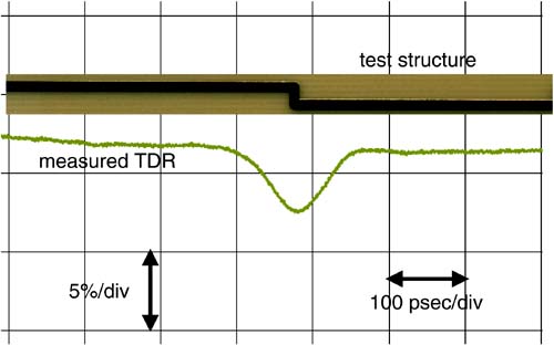
Figure 8-27. Measured TDR response of a uniform 50-Ohm line, 65 mils wide, with two 90-degree corners in close proximity. The rise time of the source is about 50 psec. Measured with an Agilent DCA 86100 and GigaTest Labs Probe Station.
Converting the 90-degree turn into two 45-degree bends will reduce this effect and using a rounded bend of constant width will reduce the impact from a corner even more. But, is the distortion from a corner a problem? Is the magnitude of the discontinuity large enough to worry about, and in what cases might a corner pose a problem? The only way to know the answer is to “put in the numbers,” and the only way to do this is to understand the root cause of why a corner affects signal integrity.
It is sometimes thought that a 90-degree bend causes the electrons to accelerate around the bend, resulting in excess radiation and distortion. As we saw in an earlier chapter, the electrons in a wire are actually moving at the slow speed of about 1 cm/sec. In fact, the presence of the corner has no impact at all on the speed of the electrons. It is true that there will be high electric fields at the sharp point of the corner, but this is a DC effect and is due to the sharp radius of the outside edge. These high DC fields might cause enhanced filament growth and lead to a long-term reliability problem, but they will not affect the signal quality.
TIP
The only impact a corner has on the signal transmission is due to the extra width of the line at the bend. This extra width acts like a capacitive discontinuity. It is this capacitive discontinuity that causes a reflection and a delay adder for the transmitted signal.
If the trace were to make the turn with a constant width, the width of the line would not change and the signal would encounter the same instantaneous impedance at each point around the turn and there would be no reflection. We can roughly estimate the extra metal a corner represents; Figure 8-28 illustrates that a corner will represent a small fraction of a square of extra metal. It is definitely less than one square, and as a very rough approximation, might be on the order of half a square of metal.
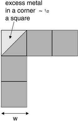
The capacitance of a corner can be estimated from the capacitance of a square and the capacitance per length of the trace:
The capacitance per length of the line is related to the characteristic impedance of the line:
So an estimate of the capacitance of a corner is roughly:
where:
Ccorner = the capacitance per corner
CL = the capacitance per length, in pF/inch
w = the line width of the line, in inches
Z0 = the characteristic impedance of the line, in Ohms
εr = the dielectric constant of the dielectric
For example, in the 0.065-inch-wide trace measured above, the estimated capacitance in each of the two 90-degree bends is about 40/50 × 2 × 0.065 = 0.1 pF = 100 fF. Since there are two in close proximity, the total capacitance of the discontinuity is estimated as about 200 fF. Using the measured TDR response, we can estimate the excess capacitance caused by the discontinuity. Figure 8-29 shows the comparison of the measured response and the simulated response of a uniform line with a lumped capacitance of 200 fF in the middle. The excellent agreement suggests the discontinuity caused by the two corners can be modeled as a 200-fF capacitor. This is very close to the 200-fF capacitance suggested by the simple model.

Figure 8-29. Measured and simulated TDR response of a uniform 50-Ohm line, 65 mils wide, with two 90-degree corners in close proximity. The rise time of the source is about 50 psec. The simulated response, based on a capacitance of 0.2 pF, is shifted down slightly for clarity. Measured with an Agilent DCA 86100 and GigaTest Labs Probe Station and simulated with TDA Systems IConnect software.
We can generalize this estimate into a simple, easy-to-remember rule of thumb:
TIP
In a 50-Ohm transmission line, the capacitance associated with a corner, in fF, is equal to 2 × the line width in mils.
As the line width gets narrower, while keeping the 50-Ohm impedance, the capacitance of a corner will decrease and its impact will be less significant. For a typical signal line in a high-density board, 5 mils wide, the capacitance of a corner is about 10 fF. The reflection noise from a 10-fF capacitor will be important for rise times on the order of 0.010 pF/4 ~ 3 psec. The delay adder from a 10-fF capacitance will be about 0.5 × 50 × 0.01 pF = 0.25 psec. It is unlikely the capacitance of a corner will play a significant signal-integrity role for 5-mil-wide lines.
If a via connects a signal line to a test point or connects signal lines on adjacent layers but continues through the entire board, the barrel of the via may have excess capacitance to the various planes in the board. This will cause a via often to look like a lumped capacitive load to a signal. The capacitance of a via will depend very strongly on the barrel size, the clearance holes, and the size of the pads on the top and bottom of the board. It can range from 0.1 pF to more than 1 pF. Any vias touching the signal line will probably look like a capacitive discontinuity, and in high-speed serial connections, are a chief limitation to the signal quality of the line.
Figure 8-30 shows the measured TDR response of a uniform line with and without a single through-hole via in the middle of a 15-inch-long line in a 10-layer board. The trace impedance is about 58 Ohms and the line width is nominally 8 mils. The rise time of the signal is about 50 psec. In this trace, the capacitance associated with both the SMA connector's via and the through-hole via in the middle of the line is about 0.4 pF. The difference in reflected voltage between the two vias is due to the rise-time degradation of the signal from dielectric losses as the signal propagates to the middle of the board and back. The changing reflected voltage along the line is a measure of the impedance variation due to manufacturing process variations.

Figure 8-30. Measured TDR response of a uniform transmission line with and without a through-hole via in the middle, creating a capacitive discontinuity. The connector via at the front of both lines is also a capacitive discontinuity. Sample provided courtesy of Doug Brooks, UltraCAD. Measured with an Agilent DCA 86100, GigaTest Labs Probe Station, and TDA Systems IConnect software.
This particular via can be approximated as a capacitance of about 0.4 pF. We would expect a delay adder from this single via to be about 0.5 × 50 × 0.4 pF = 10 psec. The transmitted signal in Figure 8-31 shows a 9-psec increase in delay time compared to a signal traveling through an identical line with no via. This is very close to the estimate based on the simple rule of thumb.
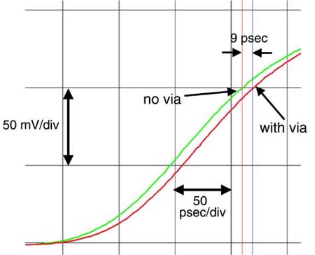
Figure 8-31. Measured transmitted signal after traveling 15 inches in a uniform transmission line and an identical line with a single through-hole via, showing a delay adder of 9 psec. Sample courtesy of Doug Brooks, UltraCAD. Measured with an Agilent DCA 86100, GigaTest Labs Probe Station, and TDA Systems IConnect software
When there is one small capacitive load on a transmission line, the signal will be distorted and the rise time degraded. Each discrete capacitance acts to lower the impedance the signal sees in its proximity. If there are multiple capacitive loads distributed on the line (for example, 2-pF connector stubs spaced every 1.2 inches for a buss, or 3-pF package and input-gate capacitances distributed every 0.8 inch for a memory buss) and if the spacing is short compared to the spatial extent of the rise time, the reflections from each capacitive discontinuity may smear out. In this case, it appears as though the characteristic impedance of the line has been reduced. The transmission line with a distribution of uniformly spaced capacitive loads is called a loaded line.
Each discontinuity will look like a region of lower impedance. When the rise time is short compared to the time delay between the capacitances, each discontinuity acts like a discrete discontinuity to the signal. When the rise time is long compared to the time delay between them, the lower impedance regions overlap and the average impedance of the line looks lower.
An example of the reflected signal from a loaded line with three different rise times is shown in Figure 8-32. In this example, there are five 3-pF capacitors distributed every 1 inch on a nominal 50-Ohm line. The last 10 inches of the line are unloaded. Each capacitor has an intrinsic 10–90 rise time of about 2.2 × 0.5 × 50 Ohms × 3 pF = 150 psec. Even though the initial rise time in the first example is 50 psec, after the first capacitor, the rise time is increased to 150 psec and longer after each capacitor.
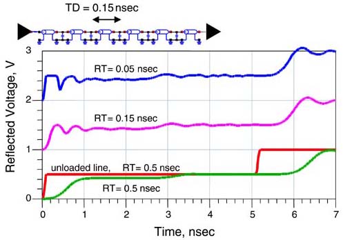
Figure 8-32. Reflected signal from a loaded line with the time delay between the 3-pF capacitors of 0.15 nsec. As the rise time increases, the reflection from each capacitor smears out.
The first few capacitors are visible as discrete discontinuities, but the later ones are smeared out by the long rise time of the transmitted signal. When the rise time of the signal is long compared to the time delay between the capacitive discontinuities, the uniformly distributed capacitive loads act to lower the apparent characteristic impedance of the line. In such a loaded line, it is as though the capacitance per length of the line has been increased by the added board features. The higher capacitance per length means a lower characteristic impedance and a longer time delay.
In a uniform, unloaded transmission line, the characteristic impedance and time delay are related to the capacitance per length and inductance per length as:
where:
Z0 = the characteristic impedance of the unloaded line, in Ohms
LL = the inductance per length of the line, in pH/inch
C0L = the capacitance per length of the unloaded line, in pF/inch
Len = the length of the line, in inches
TD0 = the time delay of the unloaded line, in psec
When there are uniformly distributed capacitive loads, each of C1 and spaced a distance of d1, the distributed capacitance per length of the line is increased from C0L to (C0L +Cl/d1). This changes the characteristic impedance of the line and its time delay to:

where:
Z0 = the characteristic impedance of the unloaded line, in Ohms
ZLoad0 = the characteristic impedance of the loaded line, in Ohms
LL = the inductance per length of the line, in pH/inch
C0L = the capacitance per length of the unloaded line, in pF/inch
C1 = the capacitance of each discrete capacitor, in pF
d1 = the distance between each discrete capacitor, in inches
Len = the length of the line, in inches
TD0 = the time delay of the unloaded line, in psec
TDLoad = the time delay of the loaded-line region
In a 50-Ohm line, the capacitance per length is about 3.4 pF/inch. When the added distributed capacitive load is comparable to this, the characteristic impedance and time delay can be changed significantly. For example, if 3-pF loads from the input-gate capacitance of a memory bank are spaced every 1 inch in a multidrop buss, the additional loaded capacitance per length is 3 pF/inch. The loaded characteristic impedance is decreased to 0.73 × Z0 and the time delay is increased to 1.37 × TD0.
Since the characteristic impedance of the line is reduced, the terminating resistance should be reduced as well. Alternatively, in the region where the distributed capacitive loads are positioned, the line width could be reduced so the unloaded impedance is higher. When the loads are attached, the loaded line impedance would be closer to the target value of the impedance.
Just about every series connection added to a transmission line will have some series loop inductance associated with it. Every via used to change signal layers, every series terminating resistor, every connector, and every engineering change wire will have some extra loop inductance. The signal will see this loop inductance as an additional discontinuity above and beyond what is in the transmission line.
If the discontinuity is in the signal path, the loop inductance will be dominated by the partial self-inductance of the signal path, though there will still be some partial mutual inductance with the return path. If the discontinuity is in the return path, the partial self-inductance of the return path will dominate the loop inductance. In either case, it is the loop inductance to which the signal is sensitive, because the signal is a current loop propagating down the line between the signal and return paths.
A series loop inductance will initially look like a higher impedance to an incident, fast rise-time signal. This will cause a positive reflection back to the source. Figure 8-33 shows the measured reflected signal from a uniform transmission line that travels over a small gap in the return path.
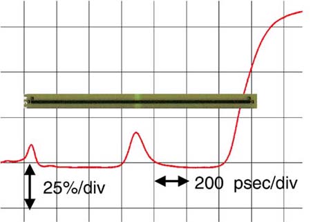
Figure 8-33. TDR-reflected signal from a uniform transmission line with an inductive discontinuity in the middle caused by a gap in the return path. The rise time is about 50 psec and was measured with an Agilent DCA 86100 and a GigaTest Labs Probe Station, analyzed with TDA Systems IConnect software.
Figure 8-34 shows the signal at the receiver and source for different values of an inductive discontinuity. The shape of the signal at the near end, going up and then back down, is called nonmonotonicity. The signal is not increasing at a steady upward pace, monotonically. This feature, by itself, may not cause a signal-integrity problem. However, if there were a receiver located at the near end, and it received a signal increasing past the 50% point and then dropping down below 50%, it might be falsely trigger. Nonmonotonic behavior is to be avoided wherever possible. At the far end, the transmitted signal will show overshoot and a delay adder.

Figure 8-34. Signal at the source and the receiver with a 50-psec rise time interacting with an inductive discontinuity. Inductance values are L = 0, 1 nH, 5 nH, and 10 nH.
In general, the maximum amount of inductance that might be acceptable in a circuit depends on the noise margin and other features of the circuit. This means that each case must be simulated to evaluate what might be acceptable. However, as a rough measure of how much inductance might be too much, we can use the limit of when the series-impedance discontinuity of the discrete inductor increases to more than 20% of the characteristic impedance of the line. At this point, the reflected signal will be about 10% of the signal swing, usually the maximum acceptable noise allocated to reflection noise.
We can approximate the impedance of the inductor if it is small compared to the characteristic impedance and if the rise time is a linear ramp, while the rise time is passing through it, by:
where:
Zinductor = the impedance of the inductor, in Ohms
L = the inductance, in nH
RT = the rise time of the signal, in nsec
The estimate of the maximum acceptable inductive discontinuity is set by keeping the impedance of the inductor less than 20% of the impedance of the line:
where:
Lmax = the maximum allowable series inductance, in nH
Z0 = the characteristic impedance of the line, in Ohms
RT = the rise time of the signal, in nsec
For example, if the characteristic impedance of the line is 50 Ohms and the rise time is 1 nsec, the maximum acceptable series inductance would be about Lmax = 0.2 × 50 × 1 nsec = 10 nH. This suggests a simple rule of thumb.
TIP
As a rough approximation, in a 50-Ohm line, the maximum allowable excess loop inductance (in nH) is 10 times the rise time (in nsec). Likewise, if there is some loop inductance from a discontinuity, the shortest rise time that might be acceptable before reflection noise exceeds the noise budget (in nsec) is L/10 with the inductance (in nH).
If there is a residual loop inductance from a connector of 5 nH, the shortest usable rise time for that connector might be on the order of 5 nH/10 = 0.5 nsec. If the rise time of the signal is 0.1 nsec, all inductive discontinuities should be kept less than 10 × RT = 10 × 0.1 = 1 nH.
Based on this estimate, we can evaluate the useful rise time for an axial lead and an SMT terminating resistor. The series loop inductance in an axial lead resistor is about 10 nH, while in an SMT resistor, it is about 2 nH.
TIP
The shortest rise time at which an axial-lead resistor might be used, before reflection noise causes a problem, is about 10 nH/10 ~ 1 nsec, while for an SMT resistor, it is about 2 nH/10 ~ 0.2 nsec.
When the rise times are in the sub-nsec regime, axial-lead resistors are not suitable components and should be avoided. As rise times approach 100 psec, it will be increasingly important to engineer the use of SMT resistors with as low a loop inductance as possible. The two most important design features of a high-performance SMT resistor are a short length and a return plane as close to the surface as possible. Alternatively, resistors that are integrated into the board or package can have considerably lower loop inductance than 2 nH and might be required.
An inductive discontinuity contributes to reflection noise and also to a delay adder. When the rise time is very short and the transmitted rise time is dominated by the series inductor, the 10–90 rise time of the transmitted signal is approximately:
where:
TD10–90 = the 10–90 rise time of the transmitted signal, in nsec
L = the series loop inductance of the discontinuity, in nH
Z0 = the characteristic impedance of the line, in Ohms
TDadder = the delay adder at the 50% point, in nsec
For example, a 10-nH discontinuity will increase the 10–90 rise time to about 10/50 = 0.2 nsec. The time delay added to the midpoint is roughly half of this or 0.1 nsec. Figure 8-35 shows the simulated time delay of the received signal with discontinuities of 1, 5, and 10 nH.
Sometimes, it is unavoidable to have a series loop inductance in a circuit, as when a specific connector has already been designed in. Left to itself, it may cause excessive reflection noise. There is a technique called compensation that is used to cancel out some of this noise.
The idea is to try to trick the signal into not seeing a large inductive discontinuity, but seeing a section of transmission line that matches the characteristic impedance of the line. After all, an ideal transmission can be approximated to first order, as an n-section of LC network. In this case, the characteristic impedance of any section of the line is given by:
where:
Z0 = the characteristic impedance of the line, in Ohms
LL = the inductance per length of the line, in nH/inch
L = the total inductance of any section of the line, in nH
CL = the capacitance per length of the line, in nF/inch
C = the total capacitance of any section of the line, in nF
An inductive discontinuity can be turned into a transmission line segment by adding a small capacitor to either side. This is illustrated in Figure 8-36. In such a case, the apparent characteristic impedance of the inductor is:

Figure 8-36. Compensation circuit for an inductive discontinuity. Add enough capacitance on either side to make the inductive discontinuity look like part of a 50-Ohm transmission line.
To minimize the reflected noise, the goal is to find values of the capacitors so that the apparent characteristic impedance of the connector, Z1, is equal to the characteristic impedance of the rest of the circuit, Z0. Using the relationship above, the capacitance to add is:
where:
C1 = the compensation capacitance to add, in nF
L1 = the inductance of the discontinuity, in nH
Z0 = the characteristic impedance of the line, in Ohms
For example, if the inductance of the connector is 10 nH and the characteristic impedance of the line is 50 Ohms, the total compensation capacitance to add is 10/502 = 0.004 nF = 4 pF. For optimum compensation, the 4-pF capacitance should be distributed with 2 pF on each side of the inductor.
Figure 8-37 shows the reflected and transmitted signals for the three cases of no connector, an uncompensated connector, and the same connector compensated. Depending on the rise time of the system, the reflected noise can sometimes be reduced by more than 75%.
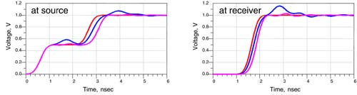
Figure 8-37. Source and transmitted signal for a 10-nH inductive discontinuity and 0.5-nsec rise time. The simulations are for no connector, with connector but no compensation, and for 2-pF capacitance added to each side of the inductor to compensate for the inductance.
This technique applies to all inductive discontinuities such as vias and resistors as well. Depending on the relative amount of capacitance in the pads and the series inductance, a real discontinuity may look capacitive or inductive.
Wherever the instantaneous impedance a signal sees changes, there will be a reflection and the transmitted signal will be distorted. This is the primary source of signal-quality problems associated with a single net.
As a rough rule of thumb, any transmission line longer, in inches, than the rise time, in nsec, will need a termination to prevent excessive ringing noise.
Source-series termination is the most common termination scheme for point-to-point connections. A series resistor should be added so that the sum of the resistor and the source impedance matches the characteristic impedance of the line.
A SPICE or behavioral simulator is essential for every engineer involved with signal integrity. Many are low cost and easy to use. These tools allow simulation of all the multiple bounces due to impedance discontinuities.
As a rough rule of thumb, variations in the characteristic impedance of a line should be kept to less than 10% to keep reflection noise less than 5%.
As a rough rule of thumb, if the length of a short transmission line discontinuity can be kept shorter, in inches, than the rise time of the signal, in nsec, the reflections from the discontinuity might not cause a problem.
As a rough rule of thumb, if the length of a short stub can be kept shorter, in inches, than the rise time of the signal, in nsec, the reflections from the stub might not cause a problem.
A capacitive load at the far end of a line will cause a delay adder but no signal quality noise.
As a rough rule of thumb, a capacitive discontinuity in the middle of a line will cause excessive reflection noise if the capacitance, in pF, is greater than four times the rise time, in nsec.
The delay adder, in psec, for a capacitive discontinuity in the middle of a line will be about 25 times the capacitance, in pF.
A corner contributes a capacitance, in fF, of about two times the line width, in mils.
A uniformly spaced distribution of capacitive loads will lower the effective characteristic impedance of the line.
The magnitude of an acceptable inductive discontinuity, in nH, is about 10 times the rise time of the signal, in nsec.
The impact from an inductive discontinuity can be greatly minimized by adding capacitance on either side of the inductor to fool the signal into seeing a section of a uniform transmission line. In this way, vias can be engineered to be nearly invisible to high-speed signals.