
The electrical description of every interconnect and passive device is based on using just three ideal lumped circuit elements (resistors, capacitors, and inductors) and one distributed element (a transmission line). The electrical properties of the interconnects are all due to the precise layout of the conductors and dielectrics and how they interact with the electric and magnetic fields of the signals.
Understanding the connection between geometry and electrical properties will give us insight into how signals are affected by the physical design of interconnects. This connection in signal integrity and interconnect design.
TIP
The key to optimizing the physical design of a system for good signal integrity is to be able to accurately predict the electrical performance from the physical design and to efficiently optimize the physical design for a target electrical performance.
All the electrical properties of interconnects can be completely described by the application of Maxwell's Equations. These four equations describe how electric and magnetic fields interact with the boundary conditions: conductors and dielectrics in some geometry. In principle, with optimized software and a powerful enough computing platform, we should be able to input the precise layout of a circuit board and all the various initial voltages coming out of the devices, push a button, and see the evolution of all the electric and magnetic fields. In principle. After all, there are no new physics or unknown, mysterious effects involved in signal propagation. It's all described by Maxwell's Equations.
There are some software tools available that, running on even a PC, will allow small problems to be completely simulated by Maxwell's Equations. However, there is no way of simulating an entire board directly with Maxwell's Equations—yet. Even if there were, we would be able to perform only a final system verification telling us that the board met or failed the performance spec. Just being able to solve for all the time-varying electric and magnetic fields doesn't give us insight into what should be changed or done differently in the next design.
TIP
The design process is a very intuitive process. New ideas come from imagination and creativity. These are fed, not by numerically solving a set of equations but by understanding, at an intuitive level, the meaning of the equations and what they tell us.
As we saw in the last chapter, the simplest starting place in thinking about the electrical performance of an interconnect is with its equivalent electrical circuit model. Every model has two parts, the circuit topology and the parameter values of each circuit element. And, the simplest starting place in modeling any interconnect is using some combination of the three ideal lumped circuit elements (resistors, capacitors, and inductors) or the distributed element (an ideal transmission line circuit element).
Modeling is the process of translating the physical design of line widths, lengths, thickness, and material properties, into the electrical view of R, L, and C elements. Figure 4-1 shows this relationship between the physical view and the electrical view for the special case of a generic RLC model.

Figure 4-1. The physical worldview and the electrical worldview of the special case of a microstrip interconnect, illustrating the two different perspectives.
Once we have established the topology of the circuit model for an interconnect, the next step is to extract the parameter values. This is sometimes called parasitic extraction. The task then is to take the geometry and material properties and ask how they translate into the equivalent parameter values of the ideal R, C, L, or T elements. We will use rules of thumb, analytic approximations, and numerical simulation tools to do this.
In this chapter, we look at how resistance is determined by the geometry and material properties. In the next three chapters, we look at the physical basis of capacitance, inductance, and transmission lines.
When we take the two ends of any conductor, such as a copper trace on a board, and apply a voltage across them, we get a current through the conductor. Double the voltage and the current doubles. The impedance across the ends of the real copper trace behaves very much like an ideal resistor. It has an impedance that is constant in time and frequency.
TIP
When we extract the resistance of an interconnect, what we are really doing is first implicitly assuming that we will model the interconnect as an ideal resistor.
Once we've established the circuit topology to be an ideal resistor element, we apply one of the three analysis techniques to extract the parameter value based on the specific geometry of the interconnect. The initial accuracy of the model will depend on how well we can translate the actual geometry into one of the standard patterns for which we have good approximations, or how well we can apply a numerical simulation tool. When we want just a rough, approximate, ball-park number, we can apply a rule of thumb.
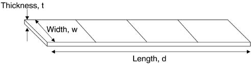
There is only one good analytical approximation for the resistance of an interconnect. This approximation is for a conductor that has a uniform cross section down its length. For example, a wire bond, a hook-up wire, and a trace on a circuit board have the same diameter or line width all down their length. This approximation will be a good match in these cases. Figure 4-2 illustrates the geometrical features for this approximation.
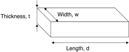
Figure 4-2. Description of the geometrical features for an interconnect that will be modeled by an ideal R element. The resistance is between the two end faces, spaced a distance, d, apart.
For the special case of a conductor with the same cross section down its length, the resistance can be approximated by:
where:
R = the resistance, in Ohms
ρ = the bulk resistivity of the conductor, in Ohm-cm
d = the distance between the ends of the interconnect, in cm
A = the cross-section area, in cm2
For example, if a wire bond has a length of 0.2 cm, or about 80 mils, and a diameter of 0.0025 cm, or 1 mil, and is composed of gold with a resistivity of 2.5 microOhm-cm, then the resistance from one end to the other will be:
TIP
This is a good rule of thumb to remember: the resistance of a 1-mil-diameter wire bond, 80 mils long, is about 0.1 Ohms.
This approximation says that the value of the resistance will increase linearly with length. Double the length of the interconnect and the resistance will double. It also varies inversely with the cross-sectional area. If we make the cross section larger, the resistance decreases. This matches what we know about water flowing through a pipe. A wider pipe means less resistance to water flow. A longer pipe means more resistance.
The parameter value of the resistance of the equivalent ideal resistor depends on the geometry of the structure and its material property (that is, its bulk resistivity). If we change the shape of the wire, the equivalent resistance will change. If the cross section of the conductor changes down its length, like it does in a lead frame of a plastic quad flat pack (PQFP), we must find a way to approximate the actual cross section in terms of a constant cross section, or we cannot use this approximation.
Consider a lead in a 25-mil pitch, 208-pin PQFP. The lead has a total length of 0.5 inch but changes its shape and does not have a constant cross section. It always has a thickness of 3 mils, but its width starts out at 10 mils and widens to 20 mils on the outside edge. How are we to estimate the resistance from one end to the other? The key term in this question is estimate. If we need the most accurate result, we would probably want to take a precise profile of the shape of the conductor and use a 3D-modeling tool that would calculate the resistance of each section, taking into account the changes in width.
The only way we can use the approximation above is if we have a structure with a constant cross section. We must approximate the real variable-width PQFP lead with a geometry that has a constant cross section. One way of doing this is to assume that the lead tapers uniformly down its length. If it is 10 mils wide on one end and 20 mils wide at the other, the average width is 15 mils. As a first pass approximation, we can assume a constant cross section of 3 mils thick and 15 mils wide. Then, using the resistivity of copper, the resistance of the lead is:
It is important to be careful with the units and always be consistent. Resistance will always be measured in Ohms.
Bulk resistivity is a fundamental material property that all conductors have. It has units of Ohms-length, such as Ohms-inches or Ohms-cm. This is very confusing. We might expect resistivity to have units of Ohms/cm, and in fact, we often see the bulk resistivity incorrectly reported with these units. However, do not confuse the intrinsic material property with the extrinsic resistance of a piece of interconnect.
Bulk resistivity must have the units it does so that the resistance of an interconnect has units of Ohms. For resistivity × length / (length × length) to equal Ohms, resistivity must have units of Ohms-length.
TIP
Bulk resistivity is not a property of the structure or object made from a material, it is a property of the material.
Bulk resistivity is an intrinsic material property, independent of the size of the chunk of material we look at. It is a measure of the intrinsic resistance to current flow of a material. The copper in a chunk 1 mil on a side will have the same bulk resistivity as the copper in a chunk 10 inches on a side.
The worse the conductor, the higher the resistivity. Usually, the Greek letter ρ is used to represent the bulk resistivity of a material. There is another term, conductivity, that is sometimes used to describe the electrical resistivity of a material. Usually, the Greek letter σ is used for the conductivity of a material. It is not surprising that a more conductive material will have a higher conductivity. Numerically, resistivity and conductivity are inversely related to each other:
While the units of resistivity are Ohms-m, for example, the units for conductivity are 1/(Ohms-m). The unit of 1/Ohms is given the special name Siemens. The units of conductivity are Siemens/meter. Figure 4-3 lists the values of many common conductors used in interconnects and their resistivity. It is important to note that the bulk resistivity of most interconnect metals will vary as much as 10% due to different processing conditions. For example, the bulk resistivity of copper is reported as between 1.5 and 1.8 µOhms-cm, depending on whether it is electroplated, electrolessly deposited, sputtered, rolled, extruded, or annealed. The more porous it is, the higher the resistivity. If it is important to know the bulk resistivity of the conductor to better than 10%, it should be measured for the specific sample.

We sometimes use the terms bulk resistivity or volume resistivity to refer to this intrinsic material property. This is to distinguish it from two other resistance-related terms, the resistance per length and the sheet resistance.
When the cross section of the conductor is uniform down the length, such as in any wire or even in a trace on a circuit board, the resistance of the interconnect will be directly proportional to the length. Using the approximation above, we can see that for a uniform cross-section conductor, the resistance per length is constant and given by:
where:
RL = resistance per length
d = interconnect length
ρ = bulk resistivity
A = cross-section area current travels through
For example, for a wire bond with a diameter of 1 mil, the cross section is constant down the length and the cross sectional area is A = π/4 × 1 mil2 = 0.8 × 10⁻⁶ inches2. With a bulk resistivity of gold of roughly 1 µOhm-inch, the resistance per length is calculated as RL = 1 µOhm-inch/0.8 × 10–6 inches2 = 0.8 Ohms/inch ~ 1 Ohm/inch.
This is an important number to keep in mind and is often called a rule of thumb: the resistance per length of a wire bond is about 1 Ohm/inch. The typical length of a wire bond is about 0.1 inch, so the typical resistance is about 1 Ohm/inch × 0.1 inch = 0.1 Ohm. A wire bond 0.05 inches long would have a resistance of 1 Ohm/inch × 0.05 inch = 0.05 Ohm or 50 mOhms.
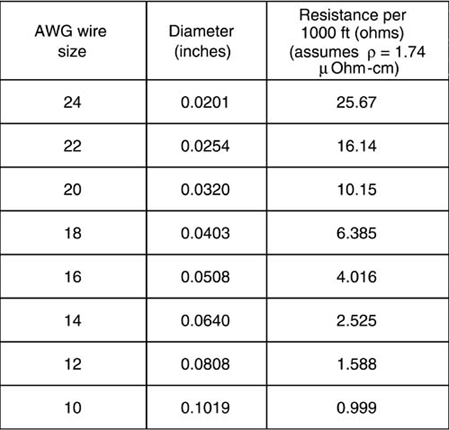
The diameter of wires is measured by a standard reference number referred to as the American Wire Gauge (AWG). Figure 4-4 lists some gauge values and the equivalent diameter. From the diameter and assuming copper wire, we can estimate the resistance per length. For example, 22-gauge wire, typical in many personal computer boxes, has a diameter of 25 mils. Its resistance per length is RL = 1.58 µOhm-cm/(2.54 cm/inch)/(π/4 × 25 mil2) = 1.2 × 10⁻³ Ohms/inch, or about 15 × 10–3 Ohms/foot or 15 Ohms per 1000 ft.
Many interconnect substrates, such as printed circuit boards, cofired ceramic substrates, and thin film substrates, are fabricated with uniform sheets of conductor that are patterned into traces. All the conductors on each layer have exactly the same thickness. For the special case, where the width of a trace is uniform, as illustrated in Figure 4-5, the resistance of the trace is given by:
The first term, (ρ/t), is constant for every trace built on the layer with thickness, t. After all, every trace on the same layer will have the same bulk resistivity and the same thickness. This term is given the special name sheet resistance and is designated by Rsq.
The second term, (d/w), is the ratio of the length to the width. This is the number of squares that can be drawn down the trace. It is referred to as n and is a dimensionless number. The resistance of a rectangular trace can be rewritten as:
where:
Rsq = the sheet resistance
n = the number of squares down the trace
Interestingly, the units of sheet resistance are just Ohms. It has units of resistance, but what resistance does sheet resistance refer to? The simplest way of thinking about sheet resistance is to consider the resistance between the two ends of a section of sheet that is one square in shape (i.e., the length equals the width). In this case, n = 1, and the resistance between the ends of the square trace is just the sheet resistance. Sheet resistance refers to the resistance of one square of conductor.
Surprisingly, whether the square is 10 mils on a side or 10 inches on a side, the resistance across opposite ends of the square is constant. If the length of the square is doubled, we might expect the resistance to double. However, the width would also double and the resistance would be cut in half. These two effects cancel and the net resistance is constant as we change the size of a square.
TIP
All square pieces cut from the same sheet of conductor have the same resistance between opposite ends and we call this resistance the sheet resistance, measured in Ohms, and often referred to as Ohms per square.
The sheet resistance will depend on the bulk resistivity of the conductor and the thickness of the sheet. In typical printed circuit boards, fabricated with layers of copper conductor, the thickness of copper is described by the weight of copper per square foot. This is a holdover from the days when the plating thickness was measured by taking a one-square-foot panel and weighing it. A 1-ounce copper gives 1 ounce of weight of copper per square foot of board. The thickness of 1-ounce copper is about 1.4 mils, or 35 microns. A 1/2-ounce copper has a thickness of 0.7 mil or 17.5 microns. Based on the thickness and the bulk resistivity of copper, the sheet resistance of 1-ounce copper is Rsq = 1.6 × 10⁻⁶ Ohm-cm /35 × 10–4 cm = 0.5 mOhm per sq.
TIP
A simple rule of thumb to remember is the sheet resistance of 1/2-ounce copper is 1 mOhm/sq. A trace 5 mil-wide and 5 inches long has 1000 squares in series and a resistance of 1 Ohm.
Sheet resistance is an important characteristic of the metallization of a layer. If the thickness and the sheet resistance are measured, then the bulk resistivity of the deposited metal can be found. Sheet resistance is measured by using a specially designed four-point probe. The four tips are usually mounted to a rigid fixture so they are held in a line with equal spacing. These four probes are placed in contact with the sheet being measured and connected to a four-point impedance analyzer or Ohmmeter. When a constant current is applied to the outer two points and the voltage is measured between the two inner points, the resistance is measured as Rmeas = V/I. Figure 4-6 illustrates the alignment of the probe points and their connection.

As long as the probes are far from the edge (i.e., at least four probe spacings from any edge), the measured resistance is completely independent of the actual spacing of the probe points. The sheet resistance, Rsq, can be calculated from the measured resistance using:
If we know the sheet resistance of the sheet, we can use this to calculate the resistance per length and the total resistance of any conductor made in the sheet. Typically, a trace will be defined by a line width, w, and a length, d. The resistance per length of a trace is given by:
where:
RL = resistance per length
R = trace resistance
Rsq = sheet resistance
w = line width
d = length of the trace
Figure 4-7 illustrates the resistance per length of different line widths for 1-ounce and 1/2-ounce copper traces. The wider the line, the lower the resistance per length, as expected. For a 5-mil-wide trace, typical of many backplane applications, a 1/2-ounce copper trace would have a resistance per length of 0.2 Ohm/inch. A 10-inch trace would have a resistance of 0.2 Ohm/inch × 10 inches = 2 Ohms.
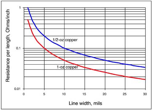
Figure 4-7. The resistance per length for traces with different line widths in 1-ounce copper and 1/2-ounce copper.
It is important to keep in mind that these resistances calculated so far are all resistances at DC, or at least at low frequency. As we show in a later chapter, the resistance of a trace will increase with frequency due to skin-depth-related effects. The bulk resistivity of the conductor does not change, the current distribution through the conductor changes. Higher-frequency signal components will travel through a thin layer near the surface, decreasing the cross-sectional area. For 1-ounce copper traces, the resistance begins to increase at about 20 MHz and will increase roughly with the square root of frequency. It's all related to inductance.
Translating physical features into an electrical model is a key step in optimizing system electrical performance.
The first step in calculating the resistance of an interconnect is assuming the equivalent circuit model is a simple ideal resistor.
The most useful approximation for the end-to-end resistance of an interconnect is R = ρ × length/cross-sectional area.
Bulk resistivity is an intrinsic material property, independent of the amount of material.
If the structure is not uniform in cross section, it must either be approximated as uniform or a field solver should be used to calculate its resistance.
Resistance per length of a uniform trace is constant. A 10-mil-wide trace in 1/2-ounce copper has a resistance per length of 0.1 Ohm/inch.
Every square cut from the same sheet will have the same edge-to-edge resistance.
Sheet resistance is a measure of the edge-to-edge resistance of one square of conductor cut from the sheet.
For 1/2-ounce copper, the sheet resistance is 1 milliOhm/square.
The resistance of a conductor will increase at higher frequency due to skin-depth effects. For 1-ounce copper, this begins above 20 MHz.