
A signal with a very fast edge going into a long transmission line will come out with a longer rise time. As an example, the measured response of a 50-psec signal transported through a 36-inch-long, 50-Ohm backplane line in FR4 is shown in Figure 9-1. The rise-time has been increased to almost 1 nsec. This rise-time degradation is due to the losses in the transmission line and gives rise to intersymbol interference (ISI) and the collapse of the eye diagram.
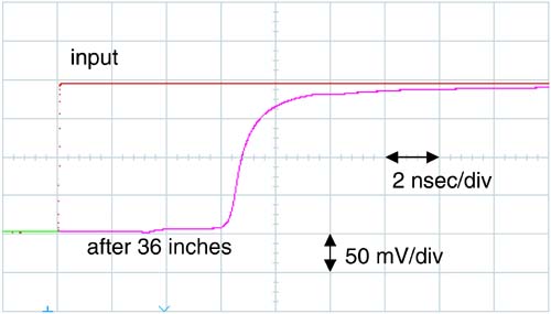
Figure 9-1. Measured input and output signals through a 50-Ohm line, 36 inches long. A 50-psec rise-time signal goes in, while a 1-nsec rise-time signal comes out.
Loss in transmission lines is the principal signal-integrity problem for all signals with clocks higher than 1 GHz, transported for distances longer than 10 inches, such as in high-speed serial links and Gigabit ethernet.
TIP
The reason the rise time is increased in propagating down a real transmission line is specifically because the higher-frequency components of the signal are preferentially attenuated more than the lower frequencies.
The simplest way to analyze the frequency-dependent losses is in the frequency domain. On the other hand, the problems created by lossy lines are time-domain dependent, and ultimately the final response must be analyzed in the time domain. In this chapter, we look first in the frequency domain to understand the loss mechanisms and then switch to the time domain to evaluate the impact on the signal-integrity response.
If the losses were independent of frequency and low-frequency components were attenuated the same as high-frequency components, the entire signal waveform would uniformly decrease in amplitude, but the rise time would stay the same. This is illustrated in Figure 9-2. The effect of the attenuation could be compensated with some gain at the receiver. The rise time, the timing, and the jitter would have remained unaffected by the constant attenuation.
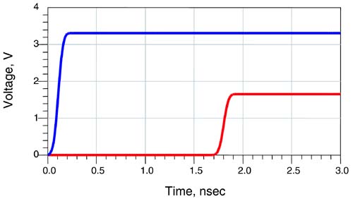
Figure 9-2. Simulated signal propagation of a 100-psec rise-time signal with losses that are independent of frequency. The only impact is a scaling of the signal.
As a signal propagates down a real lossy transmission line, the amplitudes of the higher-frequency components are reduced and the low-frequency components stay about the same. The bandwidth of the signal is decreased because of this selective attenuation. As the bandwidth of the signal decreases, the rise time of the signal increases. It is the frequency dependence of the losses that specifically drives the rise-time degradation.
If the rise-time degradation were small compared to the period for one bit, the bit pattern would be very constant and independent of what came previously. By the time one bit cycle ended, the signal would have stabilized and reached the final value. The voltage waveform for one bit in the stream would be independent of what the previous bit was, whether it was a high or a low and for how long it was high or low. In this case, there would be no ISI.
However, if the rise-time degradation increases the received rise time significantly, the actual voltage level for a bit will depend on how long the signal was at a previous high or low state. If the bit pattern was high for a long time previously and the signal drops down for one bit and then up, the low voltage will not have had time to fall all the way to the lowest voltage. The precise voltage levels achieved by a single bit will depend on the previous bit pattern. This is called intersymbol interference, or ISI, and is illustrated in Figure 9-3.
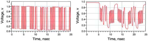
Figure 9-3. 5-GHz clock-driven pseudorandom bit stream. Left: bit pattern when the rise time is much shorter than the bit period. Right: bit pattern when the rise time is comparable to the bit pattern, causing pattern-dependent voltage levels or intersymbol interference
The important consequence of frequency-dependent loss and rise-time degradation is ISI: the precise waveform of the bit pattern will depend on the previous bits that have passed by. This will significantly affect the ability to tell the difference between a low and high level signal by the receiver, increasing the bit error rate.
TIP
In addition, the time for the signal to reach the switching threshold will change depending on the previous data pattern. ISI is a significant contributor to jitter. If the rise time were short compared to the bit period, there would be no ISI.
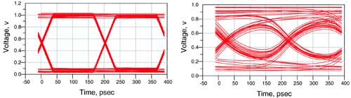
One of the common metrics for describing the signal quality of a high-speed serial link, at the receiver, is an eye diagram. A pseudorandom bit stream, whose pattern represents all possible bit-stream patterns, is simulated or measured, using the clock reference as the trigger point. Each received cycle is taken out of the bit stream and overlaid on the previous cycle and hundreds of cycles are superimposed. This set of superimposed waveforms is called an eye diagram because it looks like an open eye.
The closing of the eye diagram is a measure of the bit error rate. The smaller the opening, the higher the bit error rate. Therefore, a large opening allows the possibility of a low bit error rate and good signal quality. The horizontal width of the cross-over region that separates eye openings is a measure of the jitter. A direct consequence of frequency-dependent lossy lines and an indirect measure of the ISI is the collapse of the opening of the eye. Figure 9-4 shows the same 5-GHz clocked waveform, with and without losses, shown by the collapse of the eye diagram.
The first-order approximate model for a transmission line is an n-section LC model. This approximation is often referred to as the lossless model. It accounts for the two important features of a transmission line: characteristic impedance and time delay, but offers no process to account for the loss of the voltage as the signal propagates.
The losses need to be added to this model so that the received waveform can be accurately predicted. There are five ways energy can be lost to the receiver while the signal is propagating down a transmission line:
Radiative loss
Coupling to adjacent traces
Impedance miss matches
Conductor loss
Dielectric loss
While radiative loss is important when it comes to EMI, the amount of energy typically lost to radiation is very small compared to the other loss processes, and this loss mechanism will have no impact on lossy lines.
Coupling to adjacent traces is important and can cause rise-time degradation. This effect can be very accurately modeled and the resulting waveforms on both the active and the quiet lines predicted. In tightly coupled transmission lines, the signal on one trace will be affected by the energy coupled to the adjacent one and must be included in a critical net simulation to accurately predict performance and the transmitted signal. This topic is covered in the next chapter.
TIP
Impedance discontinuities can have a dramatic impact in distorting the transmitted signals. This will have the direct consequence of degrading the rise time of the received signal. Even a line with no loss will show rise-time degradation from impedance discontinuities. This is why it is so important to have accurate models for the transmission lines, board vias, and connectors, to accurately predict the signal quality from simulations. And this is why it is so important to minimize discontinuities in the design of high-speed interconnects.
If the rise time is degraded due to the removal of high-frequency components, where did the high-frequency components go? After all, capacitive or inductive discontinuities will not in themselves absorb energy. The high-frequency components are reflected back to the source and ultimately get absorbed and dissipated in any terminating resistors or the source impedance of the driver.
Figure 9-5 is an example of the 5-GHz clocked signal from above, as transmitted through a short, ideal, lossless transmission line with four via pads in series, each of 1-pF load, contributing a total of 4-pF capacitive load. The resulting 50% point rise-time degradation expected is about 1/2 × 50 × 4 pF = 100 psec, equal to half the bit period. Impedance discontinuities and their impact on rise-time degradation are covered in the previous chapter.

Figure 9-5. Eye diagrams of a 5-GHz clocked pseudorandom bit stream. Left: little loss. Right: same bit pattern still with no loss, but a 4-pF capacitive discontinuity from four through-hole vias.
The last two loss mechanisms represent the primary causes of attenuation in transmission lines, not taken into account by other models. Conductor loss refers to energy lost in the conductors in both the signal and the return paths. This is ultimately due to the series resistance of the conductors. Dielectric loss refers to the energy lost in the dielectric due to a specific material property—the dissipation factor of the material.
TIP
In general, with typical 8-mil-wide traces and 50-Ohm transmission lines in FR4, the dielectric losses are greater than the conductor losses at frequencies above about 1 GHz. For high-speed serial links with clock frequencies at or above 2.5 GHz, the dielectric losses dominate. This is why the dissipation factor of the laminate materials is such an important property.
The series resistance a signal sees in propagating down the signal and return paths is related to the conductors' bulk resistivity and the cross section through which the current propagates. At DC, the current distribution in the signal conductor is uniform and the resistance is:
where:
R = the resistance of the line, in Ohms
ρ = the bulk resistivity of the conductor, in Ohm-inches
Len = the length of the line, in inches
w = the line width, in inches
t = the thickness of the conductor, in inches
The DC current distribution in the return path, if it is a plane, is widely spread out through the cross section and the resistance is much smaller than the signal path's resistance and can be ignored.
For a typical 5-mil-wide trace, with 1.4-mil-thick copper (1-ounce copper), 1 inch in length, the resistance in the signal path at DC is about R = 0.72 × 10⁻⁶ Ohms-inches × 1 inch/(0.005 × 0.0014) = 0.1 Ohm.
The bulk resistivity of copper, and virtually all other metals, is absolutely constant with frequency until frequencies near 100 GHz. At first glance, we might expect the resistance of a trace to be constant with frequency. After all, this is how an ideal resistor behaves. However, as described in a previous chapter, the current will redistribute itself at higher frequencies due to skin-depth effects.
At a high frequency, the cross section through which current will be flowing in a copper conductor is in a thickness approximately equal to the skin depth, δ:
where:
δ = the skin depth, in microns
f = the sine-wave frequency, in GHz
In copper, at 1 GHz, the current in the signal path of a microstrip, for example, is concentrated in a layer about 2.5 microns thick, on either side of the trace. At 10 MHz, or 0.01 GHz, it would be concentrated in a layer about 25 microns thick. This is a rough approximation. The actual current distribution in both the signal and return paths can always be calculated with a 2D field solver. An example of the current distribution in a microstrip and a stripline for sine waves at 10 MHz is shown in Figure 9-6.
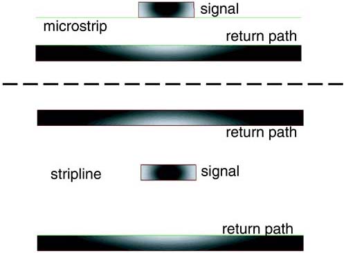
Figure 9-6. Current distribution in 1-ounce copper, for near 50-Ohm lines, at 10 MHz, showing onset of current redistribution due to skin-depth effects. Top: microstrip. Bottom: stripline. The lighter the color, the higher the current density. Simulated with Ansoft's 2D Extractor.
For 1-ounce copper, with a geometrical thickness of 35 microns, the skin depth is thinner for all frequencies above about 10 MHz. The current distribution is driven by the requirement of the current to find the path of least impedance, or at higher frequencies, the path of lowest loop inductance. This is translated into two trends: the current in each conductor wants to spread out as far apart as possible to minimize the partial self-inductance of each conductor, and simultaneously, the oppositely directed current in each conductor will move as close together as possible to maximize the partial mutual inductance between the two currents.
TIP
This means that for all important signal-frequency components, the current distribution in most PC-board interconnects is always going to be skin-depth limited, and the resistance will always be frequency dependent for frequency components above 10 MHz.
The resistance of a signal will depend on the actual cross section of the conductor transporting current. At higher frequencies, the current will be using a thinner section of the conductor and the resistance will increase with frequency. The frequency dependence of skin depth will cause a frequency dependence to resistance. It is important to note that the resistivity of copper, and most conductors, is very constant with frequency. What is changing is the cross section through which the current flows. Above about 10 MHz, the resistance per length of the signal path will be frequency dependent.
In this regime of skin-depth-limited current, if the current were flowing in just the bottom half of the conductor, the resistance of a conductor would be approximated by:
where:
R = the resistance of the line, in Ohms
ρ = the bulk resistivity of the conductor, in Ohm-inches
Len = the length of the line, in inches
w = the line width, in inches
δ = the skin depth of the conductor, in inches
As seen in the previous figure, the current flows in more than just the bottom half of the conductor, even for microstrip. There is substantial current also in the top of the conductor. These two regions are in parallel. To first order, the resistance of the signal path can be approximated as 0.5 × R, to take into account the two parallel paths in the signal path. The current distribution in the signal path of the microstrip and stripline are very similar.
Skin depth is driven by the need for the currents to take the path of the lowest impedance, which is dominated by the loop inductance at higher frequencies. This mechanism also drives the current in the return path to redistribute and change with frequency. At DC, the return current will be distributed all throughout the return plane. When in the skin-depth-limited regime, the current distribution in the return path will concentrate close to the signal path, near the surface, so as to minimize the loop inductance.
To first order, in a microstrip, the width of the current distribution in the return path is roughly three times the width of the signal path, as observed in the previous figure. This resistance in the return path is in series with the resistance of the signal path. At frequencies above about 10 MHz, we would expect the total series resistance of the transmission line to be 0.5R + 0.3R = 0.8R. The total resistance of the signal path in a microstrip is expected to be about:
where:
R = the resistance of the line, in Ohms
ρ = the bulk resistivity of the conductor, in Ohm-inches
Len = the length of the line, in inches
w = the line width, in inches
δ = the skin depth of the conductor, in inches
0.8 = a factor due to the specific current distribution in the signal and return paths
Figure 9-7 compares this simple first-order model with the results from a 2D field solver, which calculates the precise current distribution at each frequency. The agreement at both low-frequency and skin-depth-limited frequencies is excellent for so simple a model. The total resistance per length of a stripline should be slightly lower. This is also compared in the figure.

Figure 9-7. Calculated resistance vs. frequency of a 5-mil-wide, near 50-Ohm microstrip and stripline based on a field solver and the simple approximation of DC resistance and skin-depth-limited current. The circles are the microstrip and the squares are the stripline calculated with Ansoft's 2D Extractor field solver. The line is the simple first-order model of DC resistance and skin-depth-limited resistance.
So far, all we have pointed out is that the series resistance of the conductors in a transmission line will increase with increasing frequency. The question of how this frequency-dependent resistance affects loss is addressed later in this chapter.
An ideal capacitor with air as the dielectric has an infinite DC resistance. Apply a DC voltage and no current will flow through it. However, if a sine wave of voltage, V = V0 sin(wt), is applied, a cosine wave of current will flow through the capacitor, determined by the capacitance and the frequency. The current through an ideal capacitor is given by:
where:
I = the current through the capacitor
C0 = the capacitance of the capacitor
ω = the angular frequency, in radians/sec
V0 = the amplitude of the voltage sine wave applied across the capacitor
There is no loss mechanism in an ideal capacitor. The current that flows through the capacitor is exactly 90 degrees out of phase with the voltage sine wave. If the ideal capacitor were filled with an insulator with a dielectric constant of εr, the capacitance would increase to C = εr × C0.
TIP
The current through an ideal capacitor, when filled with an ideal lossless dielectric, will be increased by a factor equal to the dielectric constant. All of the current will be exactly 90 degrees out of phase with the voltage, no power will be dissipated in the material, and there is no dielectric loss.
However, real dielectric materials have some resistivity associated with them. When a real material is placed between the plates of a capacitor with a DC voltage across it, there will be some DC current that flows. This is usually referred to as leakage current. It can be modeled as an ideal resistor. The leakage resistance that is due to the material between two conductors making up a microstrip transmission line can be approximated with the parallel-plate approximation as:
The amount of leakage current that flows through this resistance is:
where:
Ileakage = the leakage current through the dielectric
V = the applied DC voltage
Rleakage = the leakage resistance associated with the dielectric
ρ = the bulk-leakage resistivity of the dielectric
σ = the bulk-leakage conductivity of the dielectric (ρ = 1/σ)
Len = the length of the transmission line
w = the line width of the signal path
h = the dielectric thickness between the signal and return paths
The leakage current, since it is going through a resistor, has current that is precisely in phase with the voltage. This current will dissipate power in the material and contribute to loss. The power dissipated by a resistor, with a constant voltage across it, is:
where:
P = the power dissipated, in watts
V = the voltage across the resistor, in Volts
R = the resistance, in Ohms
σ = the conductivity of the material
For most dielectrics, the bulk resistivity is very high, typically 1012 Ohm-cm, so the leakage resistance through a typical 10-inch-long, 50-Ohm transmission line, with w ~ 2 × h, is very high (on the order for 1011 ohms). The resulting DC power loss through this resistance will be insignificant, or less than 1 nWatt.
However, for most materials, the bulk-leakage resistivity of the material is frequency dependent, getting smaller at higher frequencies. This is due to the origin of the leakage current. There are two ways of getting leakage current through a dielectric. The first is ionic motion. This is the dominant mechanism for DC currents. The reason the DC current is low in most insulators is that the density of mobile charge carriers (i.e., ions in the case of most insulators) is very small and their mobility is so low. This is compared with the high density of free electrons in a metal and their very high mobility.
The second mechanism for current flow in a dielectric is by the re-orientation of permanent electric dipoles in the material. When a voltage is applied across a capacitor, an electric field is generated. This field will cause some randomly oriented dipoles in the dielectric to align with the field. The motion of the negative end of the dipole toward the positive electrode and the positive end of the dipole to the negative electrode looks like a transient current through the material. This is illustrated in Figure 9-8.
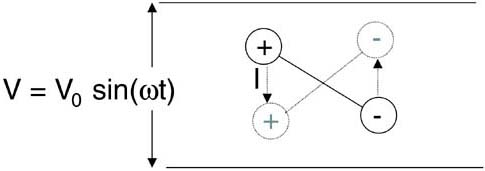
Figure 9-8. Re-orientation of the permanent dipoles in the dielectric when the external field changes is an AC current through the dielectric.
Of course, the dipoles move only a very short distance and for only a very short time. If the voltage applied is a sine wave, then the dipoles will be sinusoidally rotated back and forth. This motion gives rise to an AC current. The higher the sine-wave frequency, the faster the charges will rotate back and forth and the higher the current. The higher the current, the lower the bulk resistivity at that frequency. The resistivity of the material is decreasing with increasing frequency.
The conductivity of the material is exactly the inverse of the resistivity, σ = 1/ρ. Just as the bulk resistivity relates to the ability of the material to resist the flow of current, the bulk conductivity relates to the ability of the material to conduct current. A higher conductivity means the material conducts better. The bulk resistivity of a dielectric decreases with frequency, and the bulk conductivity increases with frequency. If the movements of the dipoles are able to follow the externally applied field and move the same distance for the same applied field, the current they create, and the bulk conductivity of the material, will increase linearly with frequency.
Most dielectrics behave in this way: their conductivity is constant from DC until some frequency is reached and then it begins to increase and continues increasing, proportional to frequency. Figure 9-9 shows the bulk conductivity of FR4 material, with the transition frequency of about 10 Hz.
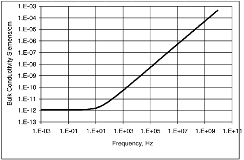
Figure 9-9. Simulated bulk conductivity of FR4 material from DC-leakage current and the AC-dipole motions.
At frequencies above this transition frequency, where the motion of dipoles plays a significant role, there can be very high-leakage current through a real capacitor, as frequency is increased. This current will be in phase with the voltage and will look like a resistor. At higher frequencies, the leakage resistance will go down and the power dissipated up causing the dielectric to heat up.
TIP
Effectively, the rotation of the dipoles translates electrical energy into mechanical energy. The friction of the motion of the dipoles with their neighbors and the rest of the polymer backbone causes the material to heat up, ever so slightly.
The actual heat energy absorbed in normal cases is so small as to contribute to a negligible temperature rise. For the case of the previous 10-inch-long, 50-Ohm microstrip, even at 1 GHz, the leakage resistance of the dielectric is less than 1 kOhm, and the power dissipated is less than 10 mWatts. However, this is not always the case for dielectric loss. The notable exception is a microwave oven. The 2.45-GHz radiation is transferred from electrical energy in the microwaves to mechanical motion and heat by the rotation of water molecules, which strongly absorb the radiation.
In transmission lines, the dielectric's dipoles will suck energy out of the signal and cause less signal at the far end. It is not enough energy to heat the substrate very much, but it is enough to cause rise-time degradation. The higher the frequency, the higher the AC-leakage conductivity, and the higher the power dissipation in the dielectric.
At low frequency, the leakage resistance of a dielectric material is constant and a bulk conductivity is used to describe the electrical properties of the material. This bulk conductivity is related to the density and mobility of ions in the material.
At high frequency, the conductivity increases with frequency due to the increasing motion of the dipoles. The more dipoles in the material that can rotate, the higher the bulk conductivity of the material. The farther the dipoles can move with an applied field, the higher the conductivity. To describe this new material property that measures the dipoles in a material, a new material electrical property must be introduced. This new material property, relating to dipole motion, is called the dissipation factor of the material:
where:
σ = the bulk AC conductivity of the dielectric
f = the sine-wave frequency, in Hz
ε0 = the permittivity of free space, 8.89 × 10⁻¹⁴ F/cm
εr = the relative dielectric constant, dimensionless
tan(δ) = the dissipation of the material, dimensionless
The dissipation factor, usually written as the tangent of the loss angle, tan(δ), is a measure of the number of dipoles in the material and how far each of them can rotate in the applied field:
where:
tan(δ) = the dissipation factor
n = the number density of dipoles in the dielectric
p = the dipole moment, a measure of the charge and separation of each dipole
θmax = how far the dipoles rotate in the applied field
As the frequency increases, the dipoles move the same distance, but faster, so the current increases and the conductivity increases. This is taken into account by the frequency term. It is important to note that in the definition of the dissipation factor, as the tangent of an angle, δ, the angle, δ, is completely unrelated and separate from the skin-depth term, which, unfortunately, also uses the Greek letter δ to describe it. It is an unfortunate coincidence that both terms relate to two different, unrelated loss processes in transmission lines. Don't confuse them.
In real materials, the dipoles can't really move the same for all applied frequencies. This slight, second-order variation of the dipole motions with frequency is taken into account by the frequency variation of θmax, which causes the dissipation factor to be slightly frequency dependent. The ability of the dipoles to move in the applied field is strongly dependent on how they are attached to the polymer-backbone chain and on the mechanical resonances of the other molecules nearby. At high enough frequency, the dipoles will not be able to respond as fast as at lower frequency and we would, therefore, expect the dissipation factor to decrease.
There is a whole field of study, called dielectric spectroscopy, that studies the frequency dependence of both the dissipation factor and the dielectric constant as a way of analyzing the mechanical properties of the polymer chains. Monitoring the dissipation factor and its frequency dependence is sometimes a measure of the degree of cure of a polymer. The more highly cross-linked the polymer, the tighter the dipoles are held and the lower the dissipation factor.
As a rough rule of thumb, the more tightly the dipoles are held by the polymer, the lower the dielectric constant and the lower the dissipation factor. The polymers with lowest dielectric constants (i.e., Teflon, silicone rubber, and polyethylene) all have very low dissipation factors. Figure 9-10 lists some commonly used interconnect dielectrics and their dissipation factors and dielectric constants.

In most interconnect materials, the dissipation factor of the material is mostly constant with frequency. Often this small variation with frequency can be neglected and a constant value used to accurately predict the loss behavior. However, there may be variations in the dissipation factor from lot to lot, from board to board, and even across the same board, due to variations in the processing of the laminate material. If the material absorbs moisture from humidity, the higher density of absorbed water molecules will increase the dissipation factor. In Polyimide or Kapton flex films, humidity can more than double the dissipation factor.
TIP
To completely describe the electrical properties of a dielectric material, two material terms are required. The dielectric constant of the material describes how the material increases the capacitance and decreases the speed of light in the material. The dissipation factor describes the number of dipoles and their motion and is a measure of how much the conductivity increases proportional to the frequency. Both terms may be weakly frequency dependent and will vary from lot to lot and board to board.
Since both terms affect electrical performance, to accurately predict perform-ance, it is important to know how these material properties vary with frequency and how they vary from board to board. If there is uncertainty in the material properties, there will be uncertainty in the performance of the circuits. Some techniques to measure these material properties at high frequency are presented later in this chapter.
Describing a term like dissipation factor as tan(δ) is a bit confusing. Why describe it as the tangent of an angle? What is it the angle of?
TIP
To use the term tan (δ) and to describe lossy lines, neither the origin of the term nor the angle to which it refers is important. It is simply a material property that relates to the number of freely moving dipoles in a material and how far they can move with frequency.
However, to use this term to evaluate the underlying mechanism for the origin of loss and to look at how to design materials to control their dissipation factor, it is important to look deeper at the real origin of dissipation factor.
A dielectric material has two important electrical material properties. One property, the relative dielectric constant, which we introduced in an earlier chapter, describes how dipoles re-align in an electric field to increase capacitance. This term describes how much the material will increase the capacitance between two electrodes and the speed of light in the material. However, it does not tell us anything about the losses in the material. A second, new material-property term, the dissipation factor, is needed to describe how the dipoles slosh back and forth and contribute to a resistance with current that is in phase with the applied-voltage sine wave.
However, both of these terms relate to the number of dipoles, how large they are and how they are able to move. When viewed in the frequency domain with applied sine-wave voltages, one term relates to the motion of the dipoles that are out of phase with the applied field and contributes to increasing capacitance, while the other term relates to the motion of the dipoles that are in phase with the applied voltage and contribute to the losses.
The current through a real capacitor, with an applied sine-wave voltage, can be described by two components. One component of the current is exactly out of phase with the voltage and contributes to the current we think of passing through an ideal lossless capacitor. The other current component is exactly in phase with the applied-voltage wave and looks like the current passing through an ideal resistor, contributing to loss.
To describe these two currents, the out-of-phase and the in-phase components, a formalism has been established based on complex numbers. It is intrinsically a frequency-domain concept because it involves the use of sine-wave voltages and currents. To take advantage of the complex number formalism, we change the dielectric constant and make it a complex number. Using the complex number formalism, the applied voltage can be written as:
The current through a capacitor is related to the capacitance by:
Using the complex number formalism, the current through the capacitor, in the frequency domain, can be written as:
This relationship describes the current through an ideal, lossless capacitor as i out of phase with the applied voltage. The i describes the phase between the current and the voltage as 90 degrees out of phase.
If the capacitor, with an empty capacitance of C0, is filled with a material that has a dielectric constant, εr, then the current through the ideal capacitor is:
Now, here's the first trick. To describe these two material properties (i.e., the dielectric constant that influences currents out of phase and the dissipation factor that influences currents in phase with the voltage), we change the definition of the dielectric constant. If the dielectric constant is a single, real number, the only current generated is i, out of phase with the voltage. If we make the dielectric constant a complex number, the real part of it will still relate to the current i out of phase, but the imaginary term will convert some of the voltage into a current in phase with the voltage and relate to the losses.
Here is the second trick. If we just describe the new complex dielectric constant as a real and imaginary term, for example, a + ib, when it is multiplied by the factor of i from the voltage, the i from the b term will convert the i term from the voltage into –1. This would make the real part of the current negative, or 180 degrees out of phase from the current. To bring the real part of the current exactly in phase with the voltage, we define the complex dielectric constant with the negative of its imaginary term. The complex dielectric constant is defined in the form:
where:
εr = the complex dielectric constant
εr' = the real part of the complex dielectric constant
εr'' = the imaginary part of the complex dielectric constant
We introduce the minus sign in the definition of the complex dielectric constant so that in this formalism, the real part of the current comes out as positive and exactly in phase with the voltage. The real part of the new, complex dielectric constant is actually what we have been calling simply the dielectric constant.
TIP
We see now that what we have traditionally called the dielectric constant is actually the real part of the complex dielectric constant. The imaginary part of the complex dielectric constant is the term that creates the current in phase with the voltage and relates to the losses.
Using this definition, the current through an ideal, lossy capacitor is given by:
where:
I = the current though an ideal, lossy capacitor, in the frequency domain
ω = the angular frequency, = 2 π × f
C0 = the empty space capacitance of the capacitor
V = the applied sine-wave voltage, V = V0 exp(iωt)
εr = the complex dielectric constant
εr' = the real part of the complex dielectric constant
εr'' = the imaginary part of the complex dielectric constant
By turning the dielectric constant into a complex number, the relationship between the in-phase and out-of-phase currents is compact. Using complex notation, we can generalize the current through a real capacitor. What makes it a little confusing is that the imaginary component of the current, which is 90 degrees out of phase with the voltage and contributes to the capacitive current with which we have been familiar, is actually related to the real part of the complex dielectric constant. The real part of the current, which is in phase with the voltage, behaves like a resistor, and contributes to loss, is actually related to the imaginary part of the dielectric constant.
As a complex number, the dielectric constant has a real part and an imaginary part. We can describe this number as a vector in the complex plane, as shown in Figure 9-11. The angle of the vector with the real axis is called the loss angle, δ. As previously noted, the use of the Greek letter δ to label the loss angle is an unfortunate coincidence with the selection of the same Greek letter to label the skin depth. These two terms are completely unrelated, as the loss angle relates to the dielectric material and the skin depth relates to the conductor properties.
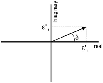
Figure 9-11. The complex dielectric constant plotted in the complex plane. The angle the dielectric-constant vector makes with the real axis is called the loss angle, δ.
The tangent of the loss angle is the ratio of the imaginary to the real component of the dielectric constant:
and
It is conventional that rather than using the imaginary part of the dielectric constant directly, the tangent of the loss angle, tan(δ), is used. In this way, the real part of the dielectric constant and tan(δ), and their possible frequency dependence, completely describe the important electrical properties of an insulating material. We also, by habit, omit the distinction that it is the real part of the dielectric constant and simply refer to it as the dielectric constant.
From the relationship above, we can relate the AC-leakage resistance of the transmission line to the imaginary part of the dielectric constant and the dissipation factor as:
In any geometrical configuration of conductors, the same geometrical features that affect the capacitance between the conductors also affect the resistance, but inversely. This is most easily seen for a parallel-plate configuration. The resistance and capacitance are given by:
Combining these two forms for the resistance between the conductors results in the connection between the bulk-AC conductivity of the material and the dissipation factor:
where:
σ = the bulk-AC conductivity of the dielectric material
ε0 = the permittivity of free space = 8.89 × 10⁻¹⁴ F/cm
εr' = the real part of the dielectric constant
εr'' = the imaginary part of the dielectric constant
tan(δ) = the dissipation factor of the dielectric
δ = the loss angle of the dielectric
R = the AC-leakage resistance between the conductors
C = the capacitance between the conductors
h = the dielectric thickness between the conductors
A = the area of the conductors
ω = angular frequency = 2 × π × f, with f = the sine-wave frequency
TIP
Even though the dissipation factor itself is only weakly frequency dependent, once again, we see that the bulk-AC conductivity of a dielectric will increase linearly with frequency due to the ω term. Likewise, since the power dissipated by the leakage resistance is proportional to the bulk-AC conductivity, the power dissipation will also increase linearly with frequency. This is the fundamental origin of the main problem lossy lines create for signal integrity.
The two loss processes for attenuating signals in a transmission line are the series resistance through the signal- and return-path conductors and the shunt resistance through the lossy dielectric material. Both of these resistors have resistances that are frequency dependent.
It is important to note that an ideal resistor has a resistance that is constant with frequency. We have shown that in an ideal lossy transmission line, the two resistances used to describe the losses are more complicated than simple ideal resistors. The series resistance increases with the square root of frequency due to skin-depth effects. The shunt resistance decreases with frequency due to the dissipation factor of the material and the rotation of dipole molecules.
In a previous chapter, we introduced a new, ideal circuit element, the ideal distributed transmission line. It was described by a characteristic impedance and a time delay. This model distributes the properties of the transmission line throughout its length. An ideal lossy distributed transmission line model will add to this lossless model two loss processes: series resistance increasing with the square root of frequency and shunt resistance decreasing inversely with frequency. This is the basis of the new ideal lossy transmission line that is implemented in many simulators. The two factors that are specified, in addition to the characteristic impedance and time delay, are the dissipation factor and resistance per length, RL, of the form:
where:
RL = the resistance per length of the conductors
RDC = the resistance per length at DC
RAC = the coefficient of the resistance per length that is proportional to f0.5
To gain insight into the behavior of ideal lossy lines, we can start with the approximation of a transmission line as an n-section LC circuit and add the loss terms and evaluate the behavior of the circuit model.
In a previous chapter, we showed that an ideal, distributed lossless transmission line can be approximated with an equivalent circuit model consisting of lumped-circuit-model sections with a shunt C and series L. This model is sometimes called the first order model of a transmission line, an n-section lumped-circuit model, or a lossless model of a transmission line. A piece of it is shown in Figure 9-12.
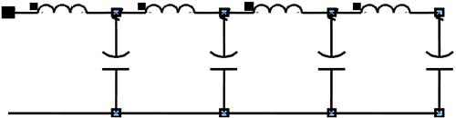
Figure 9-12. Four sections of an n-section LC model as an approximation of an ideal lossless, distributed transmission line.
This model is an approximation. However, it can be a very accurate approximation, to very high bandwidth, by using enough sections. We showed that the minimum number of sections required to achieve a bandwidth, BW, for a time delay, TD, is given by:
where:
n = the number of sections for an accurate LC model
BW = the bandwidth of the model, in GHz
TD = the time delay of the transmission line being approximated, in nsec
For example, if the bandwidth required for the model is 2 GHz, and the time delay of the line is 1 nsec, which is about 6 inches long physically, the minimum number of sections required for an accurate model is n ~ 10 × 2 × 1 = 20.
However, a significant limitation to this ideal lossless model is that it would still always be a lossless model. Using this first-order equivalent circuit model as a starting place, we can modify it to account for the losses. In each section, we can add the effect of the series resistance and the shunt resistance. A small section of the n-section lumped-circuit approximation for an ideal lossy transmission would have four terms that describe it:
C = the capacitance
L = the loop self-inductance
Rseries = the series resistance of the conductors
Rshunt = the dielectric-loss shunt resistance
If we double the length of the transmission line, the total C doubles, the total L doubles, and the total Rseries doubles. However, the total Rshunt is cut in half. If we double the length of the line, there is more area through which the AC-leakage current can flow, so the shunt resistance decreases.
For this reason, it is conventional to use the conductance of the dielectric-leakage resistance, rather than the resistance, to describe it. The conductance, denoted by the letter G, is defined as G = 1/R. Based on the resistance, the conductance is:
If the length of the transmission line doubles, the shunt resistance is cut in half but the conductance doubles. When we use G to describe the losses, we still model the losses as a resistor whose resistance decreases with frequency; we just use the G parameter to describe it. Using the conductance instead of the shunt resistance, the four terms that describe a lossy transmission line all scale with length. It is conventional to refer to their values per unit length. These four terms are referred to as the line parameters of a transmission line:
RL = series resistance per length of the conductors
CL = capacitance per length
LL= series loop inductance per length
GL= shunt conductance per length from the dielectric
We will use this ideal, second-order n-section lumped circuit model to approximate an ideal lossy transmission line, which in turn is an approximation to a real transmission line. An example of the equivalent n-section RLGC transmission-line model is shown in Figure 9-13.

Figure 9-13. Four sections of an n-section RLGC model for an ideal lossy transmission line; an approximation of an ideal distributed lossy transmission line.
The number of sections we use will depend on the length of the line and the bandwidth of the model. The minimum number of sections required is still roughly 10 × BW × TD.
This is an equivalent circuit model. We can apply circuit theory to this circuit and predict the electrical properties. The mathematics is complicated, because coupled, second-order differential equations are involved, but also because the equations are complex and the resistances have values which vary with frequency. The easiest domain in which to solve the equations is the frequency domain. We assume that signals are sine waves of voltage and, from the impedance, the sine waves of current can be calculated. The results only will be discussed.
In a lossless line, the resistance and conductance are equal to zero. This lossless circuit model would predict an interconnect that propagates a signal undistorted. The instantaneous impedance the signal sees at each step along the way is equal to the characteristic impedance of the line:
The speed of a signal is given by:
where:
Z0 = the characteristic impedance
v = the speed of the signal
CL = the capacitance per length
LL = the inductance per length
In this model, the ideal L, C, and Z0 terms as well as the time delay are all constant with frequency. These are the only terms that define the ideal, lossless transmission line. A signal entering at one end of the line will exit the other end, with no change in amplitude. The only impact on a sine wave other than a reflection due to a possible impedance change would be a phase shift in transmission.
However, when the R and G terms are added to the model, the behavior of the ideal lossy transmission line is slightly different from the ideal lossless transmission line. When the differential equations are solved, the results are rather complicated. The solution, in the frequency domain, makes no assumption on how CL, LL, RL, or GL varies with frequency. At each frequency, they may change, or they may be constant.
The final solution ends up with three important features:
The characteristic impedance is frequency dependent and complex.
The velocity of a sine-wave signal is frequency dependent.
A new term is introduced that describes the attenuation of the sine-wave amplitude as it propagates down the line. This attenuation is also frequency dependent.
When the dust clears, the exact values for the characteristic impedance, velocity, and attenuation per length are given by:

where:
Z0 = the characteristic impedance
v = the speed of a signal
αn = the attenuation per length of the amplitude, in nepers/length
ω = the angular frequency of the sine wave, in radians/sec
RL = series resistance per length of the conductors
CL = capacitance per length
LL= series loop inductance per length
GL= shunt conductance per length from the dielectric
These are formidable, and though they can be implemented in a spreadsheet, are difficult to use to gain useful engineering insight. To simplify the algebra, one of the approximations that is commonly made is that the lines are lossy, but not too lossy. This is called the low-loss approximation. The approximation is that the series resistance, RL, is RL<< ωLL and the shunt conductance, GL, is GL << ωCL.
This approximation assumes the impedance associated with the series resistance of the conductors is small compared with the series impedance associated with the loop inductance. Likewise, the shunt current through the leakage resistance of the dielectric is small compared to the shunt current through the capacitance between the signal and return paths.
For 1-ounce copper traces, the series resistance above about 10 MHz will increase with the square root of frequency and ωLL will increase linearly with frequency. At some frequency, this approximation will be good and it will get better at higher and higher frequencies.
The DC resistance per length of a 1-ounce copper trace is:
where:
RL = the resistance per length, in Ohms/inch
w = line width, in mils
Above 10 MHz, the current will flow in a thinner cross section, and rather than the geometrical thickness of 34 microns for 1-ounce copper, the skin depth will determine the thickness of the current distribution. The skin depth for copper is:
where:
δ = the skin depth, in microns
f = the sine-wave-frequency component, in MHz
The AC resistance per length of a 1-ounce copper trace, above about 10 MHz, is about:
where:
RL = the resistance per length, in Ohms/inch
δ = the skin depth, in microns
t = the geometrical thickness, in microns
w = the line width, in mils
f = the sine-wave-frequency component, in MHz
ω = the sine-wave-frequency component, in radians/sec
The inductance per length is roughly 9 nH/inch for a 50-Ohm line. The low-loss regime happens when ωLL >> RLor:
where:
RL = the resistance per length, in Ohms/inch
ω = the sine-wave-frequency component, in radians/sec for the low-loss regime
f = the sine-wave-frequency component, in Hz for the low-loss regime
w = the line width, in mils
TIP
This is a startling result. The conclusion is that for line widths wider than 3 mils, the low-loss regime is for sine-wave-frequency components well above 2 MHz. In this regime, the impedance of the series resistance is much less than the reactance of the series inductance. For lines wider than 3 mils, the low-loss regime begins at even lower frequencies. The very lossy regime is actually in the low frequency, below the frequency where skin depth plays a role.
The conductance will roughly increase linearly with frequency and the capacitance will be roughly constant with frequency. The low-loss regime happens when GL << ωCL. This is when tan(δ) << 1. For virtually all interconnect materials, the dissipation factor is less than 0.02, and the interconnect is always in the low-loss regime.
TIP
The low-loss regime for circuit-board interconnects with 3-mil-wide traces and wider is for frequencies well above 2 MHz, which is where most important frequency components are.
The conclusion is that the low-loss approximation is a very good approximation for all important frequency ranges of interest in high-speed digital applications.
In an ideal lossy transmission line, the characteristic impedance becomes frequency dependent and is complex. The characteristic impedance is given by:
With a bit of algebra, after the dust clears, the real part and imaginary part of the characteristic impedance are given by:


where:
Re(Z0) = the real part of the characteristic impedance
Imag(Z0) = the imaginary part of the characteristic impedance
RL = series resistance per length of the conductors
CL = capacitance per length
LL= series loop inductance per length
GL= shunt conductance per length from the dielectric
ω = the angular frequency
In the low-loss regime, the characteristic impedance reduces to:
The low-loss approximation for the characteristic impedance is exactly the same as for the lossless characteristic impedance. The terms that affect the characteristic impedance vary as R2 and G2 compared to ω2L2 or ω2C2. Our assumption of the low-loss regime is seen to introduce less than 1% errors, when we are at frequencies above 10 times the boundary of roughly 2 MHz for a 3-mil-wide line.
We can use the magnitude of the characteristic impedance as a rough measure of the impact from the losses. The magnitude is given by:
Figure 9-14 plots the magnitude of the complex characteristic impedance of a 3-mil-wide, 50-Ohm microstrip in FR4 using the exact relationship above. This includes the conductor loss and the dielectric loss. We see that for frequencies above about 10 MHz, the complex characteristic impedance is very close to the lossless value. This transition frequency will move toward lower frequency for wider and less lossy lines.
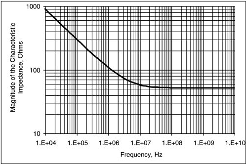
Figure 9-14. The magnitude of the complex characteristic impedance of a 50-Ohm lossy microstrip in FR4 shows that above about 10 MHz, the lossy characteristic impedance is very close to the lossless impedance. The low-loss regime is above 10 MHz.
As described earlier, there may be some frequency dependence to the inductance from skin-depth effects. Above about 100 MHz, the skin depth is much thinner than the geometrical thickness and the inductance is constant with frequency above this point. There may be some frequency dependence of the capacitance due to the real part of the dielectric constant changing with frequency. These terms may contribute to a slight frequency dependence of the characteristic impedance. In real interconnects, the impact from these effects is usually not noticeable.
A consequence of the solution to the circuit model of a lossy transmission line is that the velocity of a sine wave is complicated. The velocity is given by:

In the low-loss regime, where the impedance of the resistance is much less than the reactance of the inductance and the dissipation factor is << 0.1, the velocity can be approximated by:
This is exactly the same result as for a lossless line.
TIP
The conclusion is that in the low-loss regime, the velocity of a signal is not affected by the losses.
Using the exact form for the velocity, we can evaluate just how constant the velocity is and at what point the speed will vary with frequency. This effect is called dispersion and in this case the dispersion is caused by loss. Figure 9-15 shows the frequency dependence to the speed of a signal for a worst case of 3-mil-wide line in an FR4 50-Ohm microstrip, including both the dielectric and conductor losses.

Figure 9-15. Dispersion due to losses for a 3-mil-wide, 50-Ohm line in FR4. Plotted is the ratio of the lossy velocity to the lossless velocity.
The impact from the losses is to slow down the lower frequencies more than the higher frequencies. At lower frequencies, the series resistive impedance dominates over the series reactive impedance from the loop inductance. As well, the line looks more lossy and the signal speed is reduced. When speed varies with frequency, we call this dispersion. It arises from two mechanisms: frequency-dependent dielectric constants and losses.
Dispersion will cause the highest frequency components to travel faster than the low-frequency components. In the time domain, the fast edge will arrive first, followed by a slowly rising tail, effectively increasing the rise time. However, if the losses are ever large enough to have a noticeable impact on rise-time degradation, the impact from the attenuation will usually be far larger than the impact from dispersion.
The dominant effect on a signal from the losses in a line is a decrease in amplitude as the signal propagates down the length of the line. If a sine-wave-voltage signal with amplitude, Vin, is introduced in a transmission line, its amplitude will drop as it moves down the length. Figure 9-16 shows what the sine wave might look like at different positions, if we could freeze time and look at the sine wave as it exists on the line. This is for the case of a 1-GHz sine wave on a 40-inch-long, 50-Ohm microstrip in FR4 with a 10-mil-wide trace.

Figure 9-16. Amplitude of a 1-GHz sine-wave signal as it would appear on a 10-mil-wide, 50-Ohm transmission line in FR4.
The amplitude drops off not linearly, but exponentially, with distance. This can be described with an exponent either to base e or to base 10. Using base e, the output signal is given by:
where:
V(d) = the voltage on the line at position d
d = the position along the line, in inches
Vin = the amplitude of the input voltage wave
An = the total attenuation, in nepers
αn = the attenuation per length, in nepers/inch
When using the base e, the units of attenuation are dimensionless, but are still labeled as nepers, after John Napier, the Scotsman who is credited with the introduction of the base e exponent published in 1614. One confusing aspect of Napiers is the spelling. Napiers, napers, and nepers all refer to the same unit and are commonly used alternative spellings of his name. Though dimensionless, we use the label to remind us it is the attenuation using base e.
For example, if the attenuation were 1 napier, the final amplitude would be exp(–1) = 37% of the input amplitude. If the attenuation were 2 napiers, the output amplitude would be exp(–2) = 13% of the input voltage.
Likewise, given the input and output amplitude, the attenuation can be found from:
There is some ambiguity about the sign. In all passive interconnects, there will never be any gain. The output voltage is always smaller than the input voltage. An exponent of 0 will have exactly the same output amplitude as input amplitude. The only way to get a reduced amplitude is by having a negative exponent. Should the minus sign be placed explicitly in the exponent or be part of the attenuation? Both ways are conventionally done. The attenuation is sometimes referred to as –2 napiers or 2 napiers. Since it is always referred to as an attenuation, there is no ambiguity.
It is more common to describe attenuation using a base 10 than a base e. The output amplitude is of the form:
where:
V(d) = the voltage on the line at position d
d = the position along the line, in inches
Vin = the amplitude of the input voltage wave
AdB = the total attenuation in dB
αdB = the attenuation per length, in dB/inch
20 = the factor to convert dB into amplitude, described below
TIP
The units used to describe attenuation are in decibels, or dB. These units are used throughout engineering and wherever they appear, they leave confusion in their wake. Understanding the origin of this unit will help remove the confusion.
The decibel was created over 100 years ago by Alexander Graham Bell. He started his career as a physician studying and treating children with hearing problems. To quantify the degree of hearing loss, he developed a standardized set of sound intensities and quantified individuals' ability to hear them. He found that the sensation of loudness depended not on the power intensity of the sound, but on the log of the power intensity. He developed a scale of loudness that started with the quietest whisper that could be heard as a unit of 0 and the sound that produced pain as 10.
All other sounds were distributed on this scale, in a log ratio of the actual measured power level. If the loudness increased from 1 to 2, for example, the loudness was perceived to have doubled. However, the actual power level in the sound was measured as having increased by 102/101= 10. What Bell established is that the quality of perceived loudness change depends not on the power-level change, but on a unit that is proportional to the log of the power-level change.
The units of the Bell scale of loudness were called Bells, with 0 Bells as the quietest whisper that can be heard. The actual power density at the ear has since been quantified for each sound level. The quietest sound level that can be perceived at our peak sensitivity at about 2 kHz is the start of the scale, 0 Bell. It corresponds to a power density of 10–12 watts/m2. For the loudest sound just at the pain threshold, 10 Bells, the power level is 10–2 watts/m2.
As the Bell scale of perceived loudness gained wide acceptance, the last L was dropped and it become the Bel scale of perceived loudness. Over time, it was found that the range of the scale, 0 Bels to 10 Bels, was too small given the incredible range of perceived loudness. Instead of loudness measured in Bels, the scale was changed to decibels, where the preface “deci” means 1/10. The perceived loudness scale now starts with 0 decibels at the low end for the whisper and has 100 decibels at the onset of pain. The decibel is usually abbreviated as dB.
TIP
Over the years, the decibel scale has been adopted for other applications in addition to loudness, but in every case, the decibel has retained its definition as the log of the ratio of two powers. The most important property of the decibel scale is that it always refers to the log of the ratio of two powers.
In virtually all engineering applications, the log of the ratio of two powers, P1 and P0, is also measured in Bels: the number of Bels = log(P1/P0). Since 1 Bel = 10 decibels, the ratio, in dB, is:
For example, if the power increases by a factor of 1000, the increase, in Bels, is log(1000) = 3 Bels. In dB, this is 10 × 3 Bels = 30 dB. A decrease in the power level, where the output power is only 1% the input power, is log(10–2) = –2 Bels, or 10 × –2 Bels = –20 dB.
When the power level changes by any arbitrary factor, the change can be described in dB, but requires a calculator to calculate the log value. If the power doubles, the change in dB is 10 × log(2) = 10 × 0.3 = 3 dB. We often use the expression “a 3 dB change,” which refers to a doubling in the power level. If the change were to drop by 50%, the change in dB would be 10 × log(0.5) = –3 dB.
The ratio of the actual power levels can be extracted from the ratio in dB by:
The first step is to convert the dB into Bels. This is the exponent to base 10. For example, if the ratio in dB is 60, the power level ratio is 1060/10 = 106 = 1,000,000. If the dB value is –3 dB, the power level ratio is 10–3/10 = 10–0.3 = 0.5 or 50%
There are two rules about the dB scale that are important to always keep in mind:
The dB scale always refers to the log of the ratio of two powers or energies.
When measured in dB, the exponent to base 10 of the ratio of two powers is just the dB/10.
The distinction about power is important whenever the ratio of two other quantities is measured. When the ratio, r, of two voltages is measured, for example, V0 and V1, the units are dimensionless: r = log(V1/V0). But we cannot use dB to measure the ratio, since the dB units refer to the ratio of two powers or energies. A voltage is not an energy, it is an amplitude.
We can refer to the ratio of the powers associated with the two voltage levels, or rdB = 10 × log(P1/P0). How are the power levels related to the voltage levels? The energy in a voltage wave is proportional to the square of the voltage amplitude, or P ~ V2.
The ratio of the powers, in dB, is:

TIP
Whenever the ratio of two amplitudes is measured in units of dB, it is calculated by taking the log of the ratio of their associated powers. This is equivalent to multiplying the log of the ratio of the voltages by 20.
For example, a change in the voltage from 1 v to 10 v, measured in dB, is 20 × log(10/1) = 20 dB. The voltage increased by only a factor of 10. However, the underlying powers corresponding to the 1 v and 10 v increased by a factor of 100. This is reflected by the 20-dB change in the power level. dB is always a measure of the change in power. When the amplitude decreases to half its original value, or reduced by 50%, the ratio of the final to the initial value, in dB, is 20 × log(0.5) = 20 × –0.3 = –6 dB. If the voltage is reduced by 50%, the power in the signal must have decreased by (50%)2 or 25%. If the ratio of two powers is 25% in dB, this is 10 × log(0.25) = 10 × –0.6 = –6 dB.
TIP
When referring to an energy or power, the factor of 10 is used in calculating the dB value. When referring to an amplitude, a factor of 20 is used. An amplitude is a quantity such as voltage, a current, or an impedance.
From the ratio in dB, the actual ratio of the voltages can be calculated as:
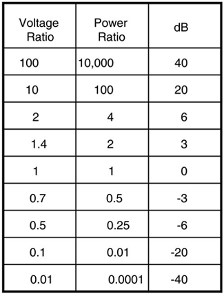
For example, if the ratio in dB is 20 dB, the ratio of the amplitudes is 1020/20 = 101 = 10. If the ratio in dB is –40 dB, the ratio of the voltages is 10–40/20 = 10–2 = 0.01. If the ratio in dB is negative, this means the final value is always less than the initial value. Figure 9-17 lists a few examples of the ratio of the voltages, their associated powers, and the ratio in dB.
When a sine-wave signal propagates down a transmission line, the amplitude of the voltage decreases exponentially. The total attenuation, measured in dB, increases with length. In FR4, a typical attenuation of a 1-GHz signal might be 0.1 dB/inch. In propagating 1 inch, the attenuation is 0.1 dB and the signal amplitude has dropped to Vout/Vin = 10–0.1/20 = 99%. In propagating 10 inches, the attenuation is 1 dB and the amplitude has dropped to Vout/Vin = 10–1/20 = 89%.
The attenuation is a new term that describes a special property of lossy transmission lines. It is a direct result of the solution of the second-order, lossy RLCG circuit model. The attenuation per length, usually denoted by alpha, αn, in nepers/length, is given by:
In the low-loss approximation, it is approximated by:
There is a simple conversion from a ratio of two voltages in nepers to the same ratio in dB. If rn is the ratio of the two voltages in nepers and rdB is the ratio of the same voltages in dB, then, since they equal the same ratio of voltages:
Using this conversion, the attenuation per length of a transmission line, in dB/length, is:
where:
αn = the attenuation of the amplitude, in nepers/length
αdB = the attenuation, in dB/length
RL = series resistance per length of the conductors
CL = capacitance per length
LL = series loop inductance per length
GL = shunt conductance per length from the dielectric
Z0 = the characteristic impedance of the line, in Ohms
Surprisingly, though this is the attenuation in the frequency domain, there is no intrinsic frequency dependence to the attenuation.
TIP
If the series resistance per length of the conductors were constant with frequency and the shunt dielectric conductance per length were constant with frequency, the attenuation of the transmission line would be constant with frequency. Every frequency would see the same amount of loss.
Every frequency would be treated exactly the same in propagating through the transmission line. Though the amplitude of the signal would decrease as it propagates through the transmission line, the bandwidth would be preserved and the rise time would be unchanged. The result would be the same rise time coming out of the line as going in.
However, as we saw earlier, this is not how real lossy transmission lines on typical laminate substrates behave. In the real world, to a very good approximation, the resistance per length will increase with the square root of frequency due to skin depth, and the shunt conductance per length will increase linearly with the frequency due to the dissipation factor of the dielectric. This means the attenuation will increase with frequency. Higher frequency sine waves will be attenuated more than lower frequency sine waves. This is the primary mechanism that will decrease the bandwidth of signals when propagating down a lossy line.
There are two parts to the attenuation per length. The first part relates the attenuation from the conductor. The attenuation from just the conductor loss is:
The second part of the attenuation relates to the losses from just the dielectric materials:
The total attenuation is:
where:
αcond = the attenuation per length from just the conductor loss, in dB/length
αdiel = the attenuation per length from just the dielectric loss, in dB/length
αdB = the total attenuation, in dB/length
RL = series resistance per length of the conductors
CL = capacitance per length
LL = series loop inductance per length
GL = shunt conductance per length from the dielectric
Z0 = the characteristic impedance of the line, in Ohms
In the skin-depth-limited regime, the resistance per length of a stripline was approximated above as:
or for frequency in GHz:
where:
RL = the resistance per length, in Ohms/inch
δ = the skin depth, in microns
t = the geometrical thickness, in microns (for 1-ounce copper)
w = the line width, in mils
f = the sine-wave-frequency component, in GHz
Combining these results, the attenuation from just the conductor is approximately:
The total attenuation from the conductor for the entire length of transmission line is:
where:
RL = the resistance per length, in Ohms/inch
w = the line width, in mils
f = the sine-wave-frequency component, in GHz
Z0 = the characteristic impedance of the line, in Ohms
Acond = the total attenuation from just the conductor loss, in dB
Len = the length of the transmission line, in inches
For example, at 1 GHz, a 50-Ohm line with a line width of 10 mils, will have an attenuation per length from just the conductor of αcond = 36/(10 × 50) × 1 = 0.07 dB/inch. If the line is 36 inches long, typical of a backplane application, the total attenuation from one end to the other would be 0.07 dB/inch × 36 inches = 2.5 dB. The ratio of the output voltage to the input voltage is Vout/Vin = 10–2.5/20 = 75%. This means that there will only be 75% of the amplitude left at the end of the line for 1-GHz frequency components as a result of just the conductor losses. Higher-frequency components will be attenuated even more. Of course, this is an approximation. A more accurate value can be obtained using a 2D field solver that allows calculation of the precise current distribution and how it changes with frequency.
Figure 9-18 compares this estimate for the attenuation from just the conductor loss to the calculated attenuation for the case of a 10-mil-wide, 50-Ohm microstrip trace using a 2D field solver. The approximation is a reasonable estimate.
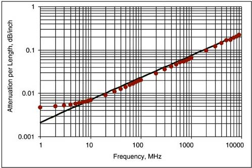
Figure 9-18. Calculated attenuation per length of a 10-mil-wide, 50-Ohm microstrip assuming only conductor loss and no dielectric loss, comparing the simple model above (line) and the simulation using Ansoft's SI2D field solver (circles).
As shown previously, for all geometries, the conductance per length is related to the capacitance per length as:
Likewise, for all geometries, the characteristic impedance is related to the capacitance as:
From these two relationships, the attenuation per length from just the dielectric material can be rewritten as:

where:
αdiel = the attenuation per length from just the dielectric loss, in dB/length
GL = the conductance per length
ω = the angular frequency, in radians/sec
tan(δ) = the dissipation factor
CL = the capacitance per length
Z0 = the characteristic impedance
εr = the real part of the dielectric constant
c = the speed of light in a vacuum
If we use units of inches/nsec for the speed of light, and GHz for the frequency, the attenuation per length from just the dielectric becomes:
where:
αdiel = the attenuation per inch from just the dielectric loss, in dB/inch
f = the sine-wave frequency, in GHz
tan(δ) = the dissipation factor
εr = the real part of the dielectric constant
What is interesting is that the attenuation is independent of the geometry. If the line width is increased, for example, the capacitance will increase so the conductance will increase, but the characteristic impedance will decrease. The product stays the same.
TIP
The attenuation due to the dielectric is only determined by the dissipation factor of the material. The attenuation due to the dielectric cannot be changed from the geometry; it is completely based on a material property.
This is not an approximation, but due to the fact that all the geometrical terms that affect the shunt conductance inversely affect the characteristic impedance, the product is always independent of geometry.
FR4 has a dissipation factor of roughly 0.02. At 1 GHz, the attenuation per length of a transmission line using FR4 would be about 2.3 × 1 × 0.02 × 2 = 0.09 dB/inch. This should be compared with the result above of 0.07 dB/inch for the attenuation per inch from the conductor for a 50-Ohm line and with a 10-mil width. At 1 GHz, the attenuation from the dielectric is slightly greater than the attenuation from the conductor. At even higher frequency, the attenuation from the dielectric will only get larger faster than the attenuation from the conductor. This means that if the dielectric loss dominates at 1 GHz, it will become more important at higher frequency and the conductor loss will become less important at higher frequency.
The attenuation from the dielectric will increase faster with frequency than the attenuation from the conductor. There is some frequency above which the attenuation will be dominated by the dielectric. Figure 9-19 shows the attenuation per length for a 50-Ohm line with an 8-mil-wide trace in FR4, comparing the attenuation from the conductor, from the dielectric, and for the total combined attenuation per length. For 50-Ohm traces wider than 8 mils, the transition frequency where dielectric and conductor losses are equal is less than 1 GHz. Above 1 GHz, the dielectric loss dominates. If the line width is narrower than 8 mils, the transition frequency is above 1 GHz.
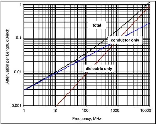
Figure 9-19. Attenuation per inch in a 50-Ohm microstrip with an 8-mil-wide trace, separating the attenuation from the conductor, the dielectric, and the total. In this geometry, with FR4, at frequencies above 1 GHz, the dielectric losses dominate the total losses.
When referring to the losses in a transmission line, there are many terms used in the industry, and unfortunately used interchangeably, even though they all refer to different quantities.
The following are some of the terms used and their real definitions:
Loss: This is the generic term referring to all aspects of lossy lines.
Attenuation: This is specific measure of the total attenuation of a line, which is a measure of the decrease in power of the transmitted signal (when measured in dB) or the decrease in amplitude (when described as a percentage transmitted signal). When measured in dB, the total attenuation of a signal will increase linearly with the length of the line. When measured in percent voltage at the output, it will decrease exponentially with increasing line length.
Attenuation per length: This is the total attenuation of the power, measured in dB, normalized to the length of the line, which is constant as long as the line parameters of the transmission line are constant. The attenuation per length is intrinsic and does not depend on the length of the interconnect.
Dissipation factor: This is the specific, intrinsic material property of all dielectrics which is a measure of the number of dipoles and how far they can move in an AC field. This is the material property which contributes to dielectric loss and may be slightly frequency dependent.
Loss angle: This is the angle, in the complex plane, between the complex dielectric constant vector and the real axis.
tan (δ): The tangent of the loss angle, which is also the ratio of the imaginary part of the complex dielectric constant to the real part of the complex dielectric constant, is also known as the dissipation factor.
Real part of the dielectric constant: The real part of the complex dielectric constant is the term associated with how a dielectric will increase the capacitance between two conductors, as well as how much it will slow down the speed of light in the material. It is an intrinsic material property.
Imaginary part of the dielectric constant: The imaginary part of the complex dielectric constant is the term associated with how a dielectric will absorb energy from electric fields due to dipole motion. It is an intrinsic material property related to the number of dipoles and how they move.
The dielectric constant: Normally associated with just the real part of the complex dielectric constant, the dielectric constant relates how a dielectric will increase the capacitance between two conductors.
The complex dielectric constant: This is the fundamental intrinsic material property that describes how electric fields will interact with the material. The real part describes how the material will affect the capacitance, the imaginary part describes how the material will affect the shunt leakage resistance.
When referring to the loss in a transmission line, it is important to distinguish the term to which we are referring. The actual attenuation is frequency dependent. However, the dissipation factor of the material, or other properties of the material, are generally only slowly varying with frequency. Of course, the only way to know this is by measuring real materials.
The ideal model of a lossy transmission line introduced here has three properties:
A characteristic impedance that is constant with frequency.
A velocity that is constant with frequency.
An attenuation that has a term proportional to the square root of frequency and another term proportional to the frequency.
The assumption here is that the dielectric constant and dissipation factor are constant with frequency. This does not have to be the case, it just happens that it is the case for most materials, or is a pretty good approximation in most cases. In real materials that have a frequency-dependent material property, it usually varies so slowly with frequency that it can be considered constant over wide-frequency ranges. The only way to know how it varies is to measure it.
Unfortunately, at frequencies in the GHz range, where knowing the material properties is important, there is no instrument that is a dissipation-factor meter. We cannot put a sample of the material in a fixture and read out the final dissipation factor at different frequencies. Instead, a slightly more complicated method must be used to extract the intrinsic material properties from laminate samples.
The first step is to build a transmission line with the laminate, preferably a stripline, so there is uniform dielectric everywhere around the signal path. In order to probe the transmission line, there will be vias at both ends. Using microprobes, the behavior of sine-wave voltages can be measured with minimal impact from the probes.
A vector network analyzer (VNA) can be used to send in sine waves and measure how they are reflected and transmitted by the transmission line. The ratio of the reflected to the incident sine wave is called the return loss or S11, and the ratio of the transmitted to the incident sine wave is called the insertion loss or S21.
These two terms, at every frequency, completely describe how sine waves interact with the transmission line. At each frequency, S11 or S21, called S or scattering parameters, describe the reflected or transmitted sine-wave amplitude and phase compared with the incident amplitude and phase. The further restriction in this definition is that reflected and transmitted sine waves are measured when a 50-Ohm source and load are connected to the ends of the transmission line.
If the characteristic impedance of the transmission line is different from 50 Ohms, there will be significant reflections, and depending on the length of the line, there will be periodic patterns in the S parameters, as the sine waves find resonances due to the length of the line and impedance discontinuities. However, we can account for all of these effects if we know the characteristic impedance of the line and the model for the vias or connectors on the ends.
The actual measured insertion loss in a 4-inch length of 50-Ohm transmission line is shown in Figure 9-20. The transmitted signal, S21, in dB, drops off roughly as the frequency increases, as expected. In this example, the transmission line is roughly 50 Ohms, and the vias do not contribute a very noticeable effect until above 8 GHz. The measured insertion loss is a rough approximation of the attenuation. When S21 is displayed in dB, the slope of the attenuation is seen to be pretty constant, as expected by the simple model.

Figure 9-20. Measured insertion loss of a 4-inch-long, nearly 50-Ohm stripline made from FR4 measured with a GigaTest Labs Probe Station.
For a perfectly matched transmission line with no vias, S21 is exactly a measure of the attenuation as a function of frequency. However, in practice, this is almost impossible to engineer, so we must interpret S21 based on a model for the transmission-line test structure, which includes the vias.
To account for the electrical effects of the vias at the ends, we can model them as a simple pi circuit with a C-L-C topology. The real transmission-line test structure can be modeled with an ideal circuit model as shown in Figure 9-21. This model is fully defined in terms of just eight parameter values:
Cvia1 = the capacitance of the first part of the via
Lvia = the loop inductance associated with the via
Cvia2 = the capacitance of the second part of the via
Z0 = the lossless characteristic impedance
εr = the real part of the dielectric constant, assumed to be constant over frequency
len = the length of the transmission line, in this case, measured with a ruler as 4 inches
tan(δ) = the dissipation factor of the laminate, assumed to be constant over frequency
αcond/f0.5 = the term related to conductor loss and normalized to the square root of the frequency
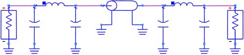
Figure 9-21. Circuit topology to model this 4-inch-long transmission line, including the VNA ports and vias at the two ends of the ideal lossy transmission line.
If we knew the values for each parameter of this model, we could simulate its insertion loss. If we had the right topology and we knew the values of each parameter, we should get very good agreement between the measured insertion loss and the simulated insertion loss.
After optimization, the best set of parameter values for each of the eight terms in the model, for this particular measured transmission line, is:
Cvia1 = 0.025 pF
Lvia = 0.211 nH
Cvia2 = 0.125 pF
Z0 = 51.2 Ohms
εr = 4.05
len = 4 inches
tan(δ) = 0.015
αcond/f0.5 = 3 dB/m/sqr(f)
In Figure 9-22, we show the comparison of the simulated insertion loss and the actual measured insertion loss using the ideal circuit model and these parameter values, which are all constant across the entire measurement bandwidth.
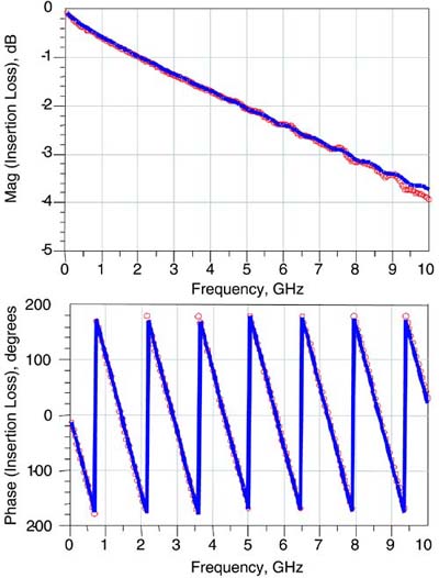
Figure 9-22. Comparing the measured and simulated insertion loss of a 4-inch-long, nearly 50-Ohm transmission line made from FR4.
The agreement is excellent between the measured insertion loss and the predicted insertion loss based on the simple ideal circuit model. This gives us confidence we have a good topology and parameter values and can conclude that the dielectric constant is 4.05 and the dissipation factor is 0.015. The assumption they are both constant across the entire measurement bandwidth of 10 GHz fits the measured data.
In Figure 9-23, the measurement bandwidth is extended up to 20 GHz for this same sample. There is excellent agreement between the measured response and the predicted response, assuming a constant dielectric constant and dissipation factor, up to about 14 GHz. Above this frequency, it appears as though the actual dissipation factor of the laminate is increasing and the dielectric constant is decreasing very slightly. From this measurement, we can identify the limit to the assumption about constant material properties. For this FR4 sample, the assumption of constant material properties is good to about 14 GHz.

Figure 9-23. Measured and simulated insertion loss extended up to 20 GHz showing 14 GHz as the bandwidth of the model. Above this frequency, it appears the actual dissipation factor may be increasing with frequency.
TIP
The fact that we get such excellent agreement between the measured insertion loss compared with the simple ideal lossy transmission-line model supports the use of this simple model to describe the high-frequency properties of real lossy transmission lines. The only caveat is that for different material systems, it is important to measure the specific material properties.
If we start with the spectrum of an ideal square wave and preferentially attenuate the higher-frequency components more than the low-frequency components, the bandwidth of the transmitted signal—the highest sine-wave frequency that is significant—will decrease. The longer we let the wave propagate, the more the attenuation of the higher-frequency components and the lower the bandwidth.
The entire concept of bandwidth as the highest sine-wave-frequency component that is significant is inherently only a rough approximation. As we have stated previously, if a problem is so sensitive to bandwidth that knowing its value to within 20% is important, the bandwidth term should not be used. Rather, the entire spectrum of the signal and actual insertion or return loss behavior of the interconnect across the whole frequency range should be used. However, the concept of bandwidth is very powerful in helping to feed our intuition and provide insight into the general behavior of interconnects.
There is a simple and fundamental connection between the bandwidth of an interconnect and the losses in the transmission line. The longer the line, the greater the high-frequency losses and the lower the bandwidth of the line. Being able to estimate the loss-limited bandwidth of an interconnect will allow us to establish some performance requirements on how much attenuation is too much and what material properties might be acceptable.
As we showed in an earlier chapter, the bandwidth of a signal is the highest frequency that has less than –3-dB amplitude compared to an ideal square-wave amplitude. At each distance, d, down the transmission line, we can calculate the frequency that has a 3-dB attenuation and is the bandwidth of the signal at that point. This frequency will be the intrinsic bandwidth of the transmission line, BWTL.
Assuming we are in a frequency regime where dielectric loss dominates, so we can ignore the resistive loss, the total attenuation at a frequency, f, and having propagated a distance, d, is:
where:
AdB = the total attenuation, in dB
αdiel = the attenuation per length from just the dielectric, in dB/inch
εr = the real part of the complex dielectric constant
d = the length of the transmission line, in inches
f = the frequency of the sine wave, in GHz
tan(δ) = the material's dissipation factor
The intrinsic bandwidth of the transmission line, BWTL, corresponds to the frequency that has an attenuation of just 3 dB. By substituting BWTL for the frequency, f, and the attenuation as 3 dB, the connection between the bandwidth and interconnect length can be found as:
where:
BWTL = the intrinsic bandwidth of the interconnect, in GHz, for a length, d, in inches
εr = the real part of the complex dielectric constant
d = the length of the transmission line, in inches
f = the frequency of the sine wave, in GHz
tan(δ) = the material's dissipation factor
This says, the longer the interconnect length, the lower the bandwidth and the lower the frequency at which the attenuation has increased to 3 dB. Likewise, the higher the value of the dissipation factor, the lower the bandwidth of the interconnect.
The rise time of an ideal square wave is 0, and the bandwidth of its spectrum is infinite. If we do something to the spectrum to decrease the bandwidth, the rise time will increase. The resulting rise time, RT, is:
where:
RT = the rise time, in nsec
BW = the bandwidth, in GHz
In a lossy interconnect, given its intrinsic bandwidth as limited by the dissipation factor of the material, we can calculate the resulting rise time of the waveform after propagating down the transmission line:
where:
RTTL = the intrinsic rise time of the transmission line, in nsec
εr = the real part of the complex dielectric constant
d = the length of the transmission line, in inches
f = the frequency of the sine wave, in GHz
tan(δ) = the material's dissipation factor
For example, a transmission line using FR4, and having a dissipation factor of 0.02, would have an intrinsic interconnect rise time for a 1-inch length of line of about 0.27 × 0.02 × 2 × 1 = 10 psec. For a length of 10 inches, the intrinsic interconnect rise time would be about 100 psec. If a 1-psec rise-time signal were sent into such a transmission line, after traveling 10 inches, its rise time would have been increased to about 100 psec due to all the high-frequency components being absorbed by the dielectric and converted into heat.
TIP
As a rough rule of thumb, the rise time of a signal propagating down an FR4 transmission line will increase its rise time by about 10 psec/inch of travel.
The actual rise time of the signal will get longer and longer as the signal propagates down the line. This intrinsic interconnect rise time is dominated by the length of the line and the dissipation factor of the laminate, and it is the shortest rise time the interconnect will support. Figure 9-24 shows the intrinsic interconnect rise time for a variety of laminate materials. It can range from 10 psec/inch in FR4 to less than 1 psec/inch in some Teflon-based laminates.

Figure 9-24. Intrinsic interconnect rise time for various laminate materials, assuming the bandwidth is limited only by dielectric loss.
In these examples, we are assuming that the line width is wide enough that the chief limitation to attenuation is the dielectric. Of course, if the line is very narrow, especially for low-loss materials, the intrinsic rise time of the interconnect will be larger than the estimate based only on dielectric loss.
When the rise time that enters is not 1 psec but some longer value, RTin, even comparable to the intrinsic rise time, the resulting output rise time, RTout, is related to the intrinsic interconnect rise time, by:
where:
RTout = the rise time coming out of the interconnect
RTin = the rise time of the signal going into the interconnect
RTTL = the intrinsic interconnect rise time
This is only a rough approximation, assuming the shape of the rising edge is Gaussian. As an example, Figure 9-25 shows a roughly 41-psec input-rise-time signal entering an 18-inch-long, FR4 transmission line. The intrinsic interconnect rise time is about RTTL = 10 psec/inch × 18 inches = 180 psec. We would expect the output rise time to be about:
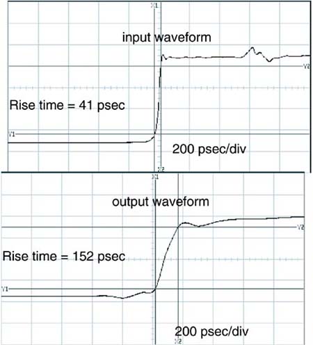
Figure 9-25. Measured rise-time degradation through an 18-inch length of FR4 trace with roughly a 50-Ohm characteristic impedance. Measured with an Agilent 54120 TDR.
In fact, what is measured is a rise time of about 150 psec, close to this estimate.
If the intrinsic interconnect rise time is much smaller than the input rise time, the output rise time is roughly the same and is unchanged. The relative change in the output rise time to the input rise time is:
To increase the output rise time by 25%, the intrinsic rise time has to be at least about 50% of the input rise time.
In FR4, with an intrinsic-rise-time degradation of about 10 psec/inch, or 0.01 nsec/inch, there is a simple rule of thumb relating the rise time and the interconnect length at which the lossy effects will be important:
TIP
This suggests that for a lossy transmission line to not appreciably degrade the rise time of the signal by more than about 25%, the intrinsic interconnect rise time must be less than 50% of the input rise time. If the initial rise time of the signal is 100 psec, the intrinsic interconnect rise time should be less than 50 psec. If it is longer, we will end up with an output rise time grossly increased.
where:
RTTL = the intrinsic interconnect rise time, in nsec/inch
RTsignal = the rise time of the signal, in nsec
d = the interconnect length, in inches, where lossy effects are important
For example, if the rise time is 1 nsec, for transmission lines longer than 50 inches, the lossy effects will degrade the rise time and potentially cause ISI problems. If the lengths are shorter than 50 inches, the lossy effects in FR4 may not be a problem. However, if the rise time were 0.1 nsec, lossy effects may be a problem for lengths longer than only 5 inches.
This is why most mother-board applications with dimensions on the order of 12 inches and typical rise times of 1 nsec do not experience problems with lossy effects. However, for backplanes, where lengths are > 36 inches and rise times are less than 0.1 nsec, lossy effects can often dominate performance.
TIP
This suggests a simple rule of thumb for estimating when to worry about lossy lines. In FR4, when the length of the line (in inches) is > 50 × the rise time (in nsec), the lossy effects may play a significant role.
Of course, this analysis is only a rough approximation. We have been assuming that we can actually use the 10–90 rise time to describe the output signal. In fact, the actual waveform gets distorted in a complex way since the higher frequency components are decreased gradually and the actual spectrum of the transmitted signal will change.
This simple rule of thumb describing the rise-time degradation through a lossy line is meant only as a way of estimating the point at which lossy-line properties will start to affect the signal quality. At this point, to accurately predict the actual waveforms and signal-quality effects, a lossy-line transient simulator should be used.
If high-frequency components are attenuated more than low-frequency components, the rise time will increase as the signal propagates. Rise time is usually defined as the time for the edge to transition between 10% and 90% of the final values. This assumes the edge profile of the signal looks somewhat Gaussian, with the middle as the fastest slope region. For this waveform, the 10%–90% rise time makes sense and has value.
However, due to the nature of the attenuation in lossy lines, the rise time is distorted and the waveform is not a simple Gaussian edge. The initial part of the waveform is faster and there is a long tail to the rising edge. If we use just one number, like the 10–90 rise time, to describe the rise time, we will have a distorted sense of when the signal has reached a level associated with a trigger threshold. In the lossy regime, rise time has less meaning and is more of a rule of thumb indicator only.
Figure 9-26 is an example of the measured input waveform and output waveform through a 15-inch-long lossy transmission line in FR4 having a dissipation factor of about 0.01. The resulting rising-edge waveform is not very Gaussian.
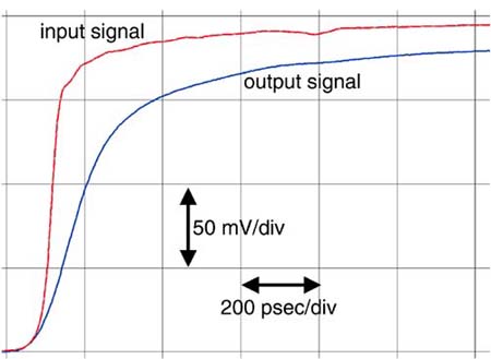
Figure 9-26. Measured rise-time degradation through a 15-inch length of FR4 trace with roughly a 50-Ohm characteristic impedance. Sample supplied by Doug Brookes and measured with an Agilent 86100, a GigaTeest Labs Probe Station, and analyzed with TDA Systems IConnect.
In comparing the actual measured S parameters of real lossy transmission lines, in the frequency domain, with the predictions of ideal lossy transmission-line models, it is clear that the simple, ideal models can work very well at frequencies at least above 10 GHz, providing we have the correct material properties.
This ideal lossy transmission-line model should be a good model to predict the time-domain behavior of real transmission lines as well. The basis of this ideal lossy transmission line model is that the series resistance is proportional to the square root of the frequency and the shunt conductance is proportional to the frequency. This is how most real lossy lines behave.
However, this is not how an ideal resistor behaves. An ideal resistor element is constant with frequency. If we use a time-domain simulator that simply has ideal resistor elements for both the series resistance and the shunt conductance, it will not be able to accurately simulate the effects of a lossy line. If the resistance is constant with frequency, the attenuation will be constant with frequency and there will be no rise-time degradation. The output rise time will look identical to the input rise time, just with slightly less amplitude.
TIP
A simulator with only a model of a resistor element with resistance constant with frequency is worthless as a lossy-line simulator. It will miss the most important impact on performance.
Using a lossy-line simulator with the ideal lossy-line model having a frequency dependent resistance and conductance, the time-dependent waveform can be evaluated. An example of a transient simulation using a lossy-line simulator is shown in Figure 9-27.
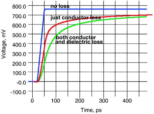
Figure 9-27. Simulated transmitted signals at the output of a 30-inch-long transmission line for a roughly 50-psec rise-time input signal with no loss, with conductor loss for an 8-mil-wide trace, and with combined conductor and dielectric loss for a dissipation factor of 0.02, showing the increasing rise-time degradation. Simulation performed with Mentor Graphics Hyperlynx.
If a similar interconnect were used with a 1-GHz clock, the resulting signal at the far end would look similar to that shown in Figure 9-28, comparing the lossless simulation with the lossy simulation for the case of 20 inches long and 40 inches long.
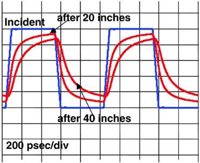
Figure 9-28. Simulated transmitted signals at the output of a 20-inch- and a 40-inch-long transmission line for a 1-GHz clock, assuming 50-Ohm line, 8-mil-wide trace, and FR4 dielectric. These signals are compared to the received signal if there were no losses. Simulation performed with Mentor Graphics Hyperlynx.
The most effective way of evaluating the impact of a lossy transmission line is by displaying the transmitted signal in an eye diagram. This shows the degree to which each bit pattern can be discerned for all combinations. A pseudorandom bit pattern is synthesized, and the transmitted signal through the interconnect is simulated. Each bit is overlaid with the previous one, synchronized to the clock. If there is no ISI, the eye pattern will be perfectly open. In other words, each bit, no matter what the previous pattern was, would look the same and be identical to the previous bit. Its eye diagram would look like just one cycle.
The degree of ISI from losses and other effects, such as capacitive discontinuities of vias, will collapse the eye diagram. If the eye collapses more than the noise margin of the receiver, the bit error rate will increase and may cause faults.
Figure 9-29 shows the simulated eye diagram for the case of a 50-Ohm, 36-inch-long backplane trace in FR4 with no losses or discontinuities, and then successively turning on the resistive loss, the dielectric loss, and one 0.5-pF via at either end of the line. The line width in this example is 4 mils. The stimulating source has a bit period of 200 psec, corresponding to a bit rate of 5 Gbps.

Figure 9-29. Simulated transmitted signals at the output of a 36-inch- long, 50-Ohm FR4 backplane trace, successively adding the effects of conductor loss, dielectric loss, and two vias. Simulation performed with Mentor Graphics Hyperlynx.
In the final simulation which includes the losses and capacitive load from the vias, the eye is substantially closed and would not be usable at this bit rate. For acceptable performance, the transmission line would have to be improved or signal-processing techniques used to enhance the opening of the eye diagram.
There are three board-design factors that influence the quality of the eye diagram:
Capacitive discontinuities from the vias
Conductor loss
Dielectric loss
If the rise-time degradation is a problem, these are the only board-level features that will affect the performance.
The first step is to design the sensitive lines with a minimum number of vias. Then optimize the hole size, antipad clearance holes, and capture pads in order to match the via capacitance to the loop inductance of the signal and return paths so the via approximates the impedance of the transmission line. This will minimize the rise-time degradation. This is similar to the compensation technique for connectors, discussed in an earlier chapter.
The total capacitance of the via between the signal and return paths should be:
For example, if the loop inductance associated with the signal via and its return path is 0.3 nH, which is a typical value in a 6-layer board, and the impedance of the line in which the via is embedded is 50 Ohms, the total capacitance of the via should be Cvia = 0.3/2500 = 0.12 pF. This should be distributed between the top and bottom surfaces of the via. This value is smaller than that for most fabricated vias.
TIP
In general, because of the size of the capture pads typically used for the top and bottom surfaces, fabricated vias have excess capacitance. If they are designed with minimal pads and extra large clearance holes in the planes, they will be better matched to the transmission line and cause less rise-time degradation.
The line width of the signal trace will be the dominant term affecting the attenuation from the conductor losses, providing the dielectric thickness is changed to keep the impedance of the line at a fixed target. A wider line width will decrease the conductor loss. If the line width is increased, the dielectric thickness would have to increase as well. This is not always practical and thus sets a limit to how wide a line can be used.
Depending on the bandwidth of interest, there is little impact from making the line too wide, because the dielectric loss may dominate. Figure 9-30 shows the impact on the attenuation per length of a 50-Ohm line, with FR4 dielectric. If decreasing attenuation is important, the first goal is to use wide lines and avoid line widths less than 5 mils if at all possible. However, making the line width wider than 10 mils does not significantly decrease the attenuation because of the dielectric losses in the FR4.
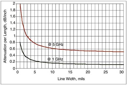
Figure 9-30. Total attenuation per length for a 50-Ohm line in FR4, as the line width is increased, assuming the dielectric thickness is also increased to keep the impedance constant.
TIP
This suggests that with FR4-laminate lines, the optimum line width for minimal attenuation is around 5 mils to 10 mils wide.
If vias are optimized and the line width is kept to 10 mils, the only other term to adjust is the dissipation factor of the laminate. Figure 9-31 shows a similar attenuation curve for two different dissipation-factor materials, both at 5 GHz. A lower-dissipation factor will always contribute to a lower attenuation. Again, we see there is a point of diminishing returns in increasing the line width even for a low-loss laminate. Much beyond 20 mils, the attenuation is dominated by the laminate material. This is why an important element to predicting high-speed performance of interconnects is having accurate values for the material properties.
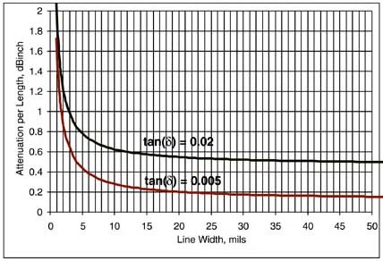
If the interconnect losses cause the eye to close, there is a trick that can be done to open the eye back up. If we send a sharp voltage step through the interconnect, it will be distorted by the time it exits the interconnect. If we can predict the degree of distortion, we can predistort the signal so that after propagating down the interconnect, the signal will approximate the sharp voltage step.
There are two ways of distorting the waveform. The fast-rising edge, which has the high-frequency components, will be attenuated more than the slow rising edge. If we take out some of the low-frequency components, we will equalize its spectrum to the high-frequency components that will be left at the end. This can be done with a simple filter. When we filter out the low-frequency components to match them to the attenuated high-frequency components, we call this equalization.
Alternatively, we can add extra high-frequency components to the initial signal, so that by the time the edge reaches the far end, these higher frequency components have attenuated back in line with the low-frequency components. This is called pre-emphasis.
Using either technique requires that the distortions of the interconnect are predictable and reproducible. This can happen only if the material properties of the laminate are known.
The fundamental problem caused by lossy lines is rise-time degradation, which results in pattern-dependent noise, also called intersymbol interference, or ISI.
The frequency-dependent losses in circuit-board interconnects arise from the conductor losses and dielectric losses.
The rise time of a signal is increased when propagating down a lossy line because the higher frequencies are attenuated more than the low frequencies. This results in a decrease in the bandwidth of the propagating signal.
At about 1 GHz, for line widths of about 8 mils, the contributions from the two losses are comparable. At a higher frequency, the dielectric losses increase in a manner that is proportional to the frequency, while the conductor losses increase in a manner that is proportional to the square root of the frequency.
The characteristic impedance of the line and the speed of a signal are not affected by the losses above just a few MHz.
At frequencies above 1 GHz, the dielectric losses dominate and the dielectric's dissipation factor is the most important material term that describes the lossy behavior of a material. Better materials will have a lower dissipation factor. FR4, with a dissipation factor of about 0.02, is the worst behaving material.
The lossy behavior of a transmission line is very accurately predicted with a lossy-line model that uses a resistance per length proportional to the square root of frequency and a shunt conductance that is proportional to frequency. This model accounts for ISI.
In addition to the material losses, any impedance discontinuities such as via pads, can degrade the rise time and contribute to ISI. The chief impact from a via is not from the inductance of the via, but from the excess capacitance of the capture pads and the capacitance between the barrel and internal planes of the board. Matching the capacitance to the inductance for a 50-Ohm line can make the via disappear.
As a rough rule of thumb, the dielectric losses in FR4 will degrade the rise time by about 10 psec per inch of travel. After 10 inches, the rise time can be increased to 100 psec.