OTA Design
This chapter is devoted to simplified design with operational transconductance amplifiers, or OTAs. An OTA is similar to the op-amps described in Chapter 3. However, OTAs and op-amps are not always interchangeable. For that reason, an explanation of unique characteristics found in OTAs is in order. The OTA not only includes the usual differential inputs of an op-amp, but also contains an additional control input in the form of an amplifier bias current or IABC. This control increases flexibility of the OTA for use in a wide range of applications.
The characteristics of an ideal OTA are similar to those of an ideal op-amp except that the OTA has an extremely high output impedance. Because of this difference, the output signal of an OTA is best described in terms of current that is proportional to the difference between the voltages at the two inputs (inverting and noninverting). The OTA transfer characteristics (or input/output relationships) are best defined in terms of transconductance rather than voltage gain. Transconductance (usually listed as gm or g21) is the ratio between the difference in current output (Iout) for a given difference in voltage input (Ein). Except for the high output impedance and the definition of input/output relationships, OTA characteristics are similar to those of a typical op-amp.
4.1 Basic OTA Circuits
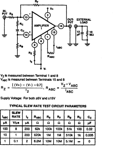
Figure 4-1 shows a simplified circuit diagram of an OTA (one of three identical circuits in the Harris CA3060). The output signal is a “current” that is proportional to the OTA transconductance (established by the IABC) and the differential input voltage. The OTA can either source or sink current at the output, depending on the polarity of the input signal.
4.2 Definition of OTA Terms
The following is a summary of terms commonly found in OTA literature:
Amplifier bias current or IABC is the current supplied to the amplifier bias terminal to establish the operating point (such as the IABC current at the base of Q3 in Fig. 4-l).
Amplifier supply current or IA is the current drawn by the amplifier from the positive supply source. The total supply current (which includes the sum of the amplifier supply current, the amplifier bias current, and the regulator bias current) is not to be mistaken for the amplifier supply current.
Bias regulator current is the current flowing from the zener bias regulator (such as at terminal 2 of Fig. 4-1) set by an external source, which establishes the operating conditions of the bias regulator.
Bias terminal voltage or VABC is the voltage existing between the amplifier bias terminal and the negative supply voltage terminal (such as between the IABC terminal and terminal 8 of Fig. 4-1).
Peak output current or IOM is the maximum current drawn from a short circuit on the amplifier output (positive IO) or the maximum current delivered into a short-circuit load (negative IO). Peak-to-peak current swing is twice the peak output current.
Peak output voltage or VOM is the maximum positive voltage swing (VOM+) or the maximum negative voltage swing (VOM–) for a specific supply voltage and amplifier bias.
Power consumption of P is the product of the sum of the supply voltage and the supply current, or (V+ plus V–) × IA. This is not the total power consumed by an operating circuit. The power in the regulator must also be included for total power consumed.
Zener regulator voltage or VZ is the regulator voltage (such as across terminals 1 and 8 of Fig. 4-1), measured with current flowing in the bias regulator.
Unlike conventional op-amps, the characteristics of OTAs can be altered by adjusting IABC. In effect, many of the OTA characteristics can be programmed to meet specific design problems. The following is a summary of the effects of IABC on typical OTAs. Note that the characteristics listed here for OTAs are the same as for op-amps (Chapter 3).
Input offset current is directly affected by IABC, and increases almost in direct proportion with increases in IABC. The same is essentially true for input bias current, amplifier supply current, device dissipation, transconductance, and peak output current.
Input offset voltage is not drastically affected by variations in IABC. A possible exception is when the OTA is operated at high temperatures. The same is essentially true of peak output voltage, which is set (primarily) by supply voltage, as is the case with a conventional op-amp.
Input and output capacitance, as well as amplifier bias voltage, increase with IABC, but not in direct proportion. That is, a large increase in IABC produces a small increase in input/output capacitance and amplifier bias voltage.
Input and output resistances both decrease with increases in IABC.
4.3 Basic OTA Design Procedures
Figure 4-2 shows a basic OTA circuit, complete with external circuit components. The following paragraphs provide a specific design example for the circuit.

FIGURE 4-2 Basic OTA circuit (20-dB amplifier) (Harris Semiconductor, Linear & Telecom ICs, 1994, p. 2–58)
Assume that the circuit is to provide a closed-loop gain of 10 (20 dB), the input offset voltage must be adjustable to zero, current drain must be as low as possible, the supply voltage is ± 6 V, maximum input voltage is ±50 mV, input resistance is 20 k, and load resistance is 20 k.
4.3.1 Transconductance
As in the case of a conventional op-amp, closed-loop gain is set by the ratio of feedback resistance RF to input resistance RS. With RS specified as 20 k and a desired closed-loop gain of 10, the value of RF is 10 × 20, or 200 k.
The next step is to calculate the required transconductance (gm or g21) to provide a suitable open-loop gain. Assume that the open-loop gain AOL must be at least 10 times the closed-loop gain. With a closed-loop gain of 10, then open-loop gain must be 10 × 10, or 100.
Open-loop gain is related directly to load resistance RL and transconductance. However, the actual load resistance is the parallel combination of RL and RF, or about 18 k (RL × RF/RL + RF). With an AOL of 100 and an actual load of 18 k, the gm should be 100/18,000, or about 5.5 millimho (mmho).
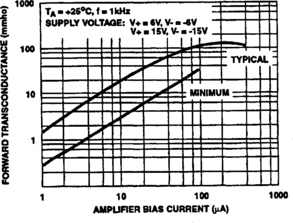
The transconductance is set by IABC. With a data sheet curve similar to that of Fig. 4-3, select an IABC from the minimum-value curve to assure that the OTA provides sufficient gain. As shown in Fig. 4-3, for a gm of 5.5 mmho, the required IABC is approximately 20 µA.
4.3.2 Output Swing
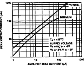
Before going on to find the value of RABC that produces 20 µA of IABC, make certain that 20 µA will provide the required output swing. With an input of ±50 mV and a gain of 10, the output swing is ±0.5 V. This output appears across the output load of about 18 k. With a 0.5-V swing and approximate load of 18 k, the total amplifier-current output is about 0.5/18 k, or 27.7 µA. With a data sheet curve similar to that seen in Fig. 4-4, use the minimum-value curve to check that an IABC of 20 µA produces an IOM of at least 27.7 µA. As shown by Fig. 4-4, an IABC of 20 µA produces an IOM of about 40 µA, well above the required 27.7 µA.
4.3.3 Calculating RABC
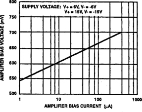
As shown in Fig. 4-2, RABC is connected to the +6-V supply. With this arrangement, RABC and diode D1 are in series between the +V and –V supplies, and there is a total of 12 V across the series components (Fig. 4-1). The drop across D1, which is VABC, can be found by reference to a curve similar to that of Fig. 4-5, which shows that an IABC of 20 µA produces a VABC of about 0.63 V. The drop across RABC is 12 – 0.63 V, or 11.37 V. For a drop of 11.37 V and an IABC of 20 A, the value of RABC is 11.37/20, or about 568 k. Use the next lowest standard resistor of 560 k, as shown in Fig. 4-2, to assure that the minimum IABC is 20 µA.
4.3.4 Input Offset Circuit
The next step is to calculate values for the input-offset adjustment circuit ROFFSET and the resistors at the noninverting input. To reduce the loading effect of the offset circuit on the power supply, the values should be selected as in the case of an op-amp. For example, the value the resistor between the input and ground should be about equal to the parallel combination of RF and RS, or about 18 k.
With a data sheet curve similar to that of Fig. 4-6, find the input offset current. As shown, for an IABC of 20 µA the input offset current should be a maximum of 200 nA. With 200 nA flowing through the input/ground (18 k) resistor, the voltage across the resistor is 200 nA × 18 k, or 3.6 mV. This 3.6 mV must be added to the maximum input-offset voltage possible for the OTA. The data sheet shows a maximum input-offset of 5 mV. Thus, the maximum voltage required at the noninverting input is 5 mV + 3.6 mV, or 8.6 mV.
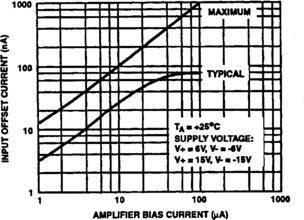
FIGURE 4-6 Input offset current versus amplifier bias current (Harris Semiconductor, Linear & Telecom ICs, 1994, p. 2–55)
The current necessary to provide a possible offset voltage of 8.6 mV across the 18-k resistor is about 0.48 µA. This current must flow through the resistor connected between the input and the ROFFSET pot. A possible ±6 V is available from ROFFSET to the resistor. However, for a more stable circuit, assume that ± 1 V is available to the resistor. With 1 V available and a required current of 0.48 µA, the value of the resistor is about 2 M. Use the next larger standard value of 2.2 M. The value of ROFFSET is not critical. A larger value of ROFFSET draws less current from the supplies. As a guideline, the maximum value of ROFFSET should be less than twice the value of the 2.2-M resistor, or less than 4.4 M in this case. Use a standard value of 4 M.
4.3.5 Capacitance Effects
Because the IC operates at low power, the external circuits must be high impedance. In designing such circuits, particularly feedback amplifiers, stray circuit capacitance must always be considered because of the adverse effect on frequency response and stability. For example, a 10-k load with a stray capacitance of 15 pF has a time constant to 1 MHz. Figure 4-7 shows how a 10-k/15-pF load modifies the frequency characteristics of the IC.

FIGURE 4-7 Effect of capacitive loading on frequency response (Harris Semiconductor, Linear & Telecom ICs, 1994, p. 2–59)
Capacitive loading also has an effect on slew rate. Because the peak output current is established by the amplifier bias current (Fig. 4-4), the maximum slew rate is limited to the maximum rate at which the capacitance can be charged by the IOM. Slew rate = dV/dt = IOM/CL, where CL is the total load capacitance, including strays. This relationship is shown graphically in Fig. 4-8.

4.3.6 Phase Compensation
Phase compensation of the IC is not required in most applications. When needed, compensation can be accomplished with an RC network at the input of the amplifier as shown in Fig. 4-9. (Compare this circuit to that shown in Fig. 3-17 for op-amps.) The values shown in Fig. 4-9 provide stable operation for the critical unity-gain condition, assuming that capacitive loading on the output is 13 pF or less. Input phase compensation is recommended to maintain the highest possible slew rate.