
Amplifier Circuit Basics
This chapter is devoted to basic amplifier circuits and characteristics. It is possible to design amplifier circuits “from scratch.” However, amplifiers are available in integrated circuit (IC) form, and it is generally simpler to use such ICs.
The data sheets for IC amplifiers often show the connections and provide all necessary design parameters to convert the IC to a complete amplifier by adding external components. This chapter describes the functions and operation of IC amplifiers to help you understand the data sheet information.
For our purposes, the function of an amplifier is to increase the amplitude of a voltage, current, or power. Secondary functions are to isolate signal sources from other circuits and to provide impedance matching. In both discrete and IC amplifiers, an input signal (consisting of a voltage or current having a definite waveform) produces a corresponding output signal with the same waveform, but in amplified form. Thus, an amplifier is a circuit which develops a voltage or current (or power) that has an amplitude greater than the control factor (or input).
1.1 Amplifier Circuit Classifications
There are many ways to classify amplifier circuits. One method is to classify the amplifier as to basic circuit connections. Depending on the circuit configuration, three basic classifications are applied to two-junction or bipolar transistors: common emitter, common base, and common collector. Note that the word grounded can be substituted for the word common in describing the three amplifier circuit configurations. Also note that in this book, the word transistor implies a two-junction or bipolar transistor. Field-effect transistor amplifiers are identified as FET amplifiers.
Amplifiers also can be classified in terms of operating point (or bias that establishes operating point). There are four commonly used operating point classifications: class A, class B, class AB, and class C. There also is a class D used to indicate the operating point of a square-wave amplifier. However, we are not concerned with such circuits in this book, except for the response of amplifier circuits to square waves. This is because square waves often are used to test amplifier characteristics and performance (as discussed in Chapter 2).
Another method of amplifier circuit classification is based on the function to be performed by the amplifier. Using this system, there are voltage amplifiers and power amplifiers. When more than one transistor is used for either function, the circuit is sometimes referred to as a compound amplifier.
Amplifiers are sometimes grouped according to frequency of operation: AF (audio frequency), RF (radio frequency), VF (video frequency), and IF (intermediate frequency). The frequency system is further broken down into narrowband (where amplification is limited to a specific frequency or a narrow range of frequencies), wideband (where a wide range of frequencies is amplified at or about the same level), tuned (where amplification is limited to a specific frequency, or to a narrow range, by tuning controls), and untuned (where the frequency range is set by nonadjustable component values).
Amplifiers also can be classified by the type of signals being amplified. For example, there are AC (alternating-current), DC (direct-current), and pulse amplifiers. From a practical standpoint, the DC amplifier also amplifies AC signals. (However, the reverse is not true.) Furthermore, many AC and DC amplifiers pass pulse or square-wave signals without difficulty.
Note that the term “DC amplifier” can mean either direct-coupled amplifier or direct-current amplifier. This confusion arises from the fact that all direct-current amplifiers must be direct coupled. That is, there must be no capacitors between stages. However, note that direct-coupled amplifiers are not limited to direct-current amplification. In general, direct-coupled amplifiers operate with alternating current and pulse signals, as well as with direct current. Note that most IC amplifiers contain many direct-coupled or d-c amplifier stages.
In addition to the various classifications, amplifiers can be assigned some specific title that is descriptive of the function or circuit configuration. A few of these are the operational amplifier (or op-amp), differential amplifier, chopper-stabilized, Norton, current-feedback, wideband, programmable op-amp, operational-transconductance amplifier (or OTA), high-speed, video, and instrumentation. In this book, we are concerned with amplifiers that are readily available in IC form.
1.2 Common-Emitter Amplifier
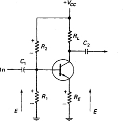
Figure 1-1 shows NPN and PNP transistors connected in a theoretical common-emitter circuit. Figure 1-2 shows a practical common-emitter or circuit operated from a single power supply. In both the theoretical and practical configurations, the base-emitter circuit is forward biased, with the base-collector circuit reverse biased. The common-emitter circuit is the most widely used amplifier configuration. The emitter is common to both the input and output circuits, and is frequently called the grounded element (although the emitter is not always connected to ground).


One reason for the popularity of the common-emitter amplifier is because both current gain and voltage gain are possible (as shown by the characteristics of Fig. 1-1). This combination results in a large power gain. For example, if the output impedance is 10 times greater than the input impedance, there is a power gain of 10, even if the base-emitter (input) and emitter-collector (output) currents are equal (no current gain). Because it is possible to control a large output current with a small input current in a common-emitter circuit, there is also current gain.
C1 is a coupling capacitor used to block out any DC components in the input signal developed across R1. Note that R1 also provides a closed circuit for current flow in the base-emitter circuit. This is essential in any transistor amplifier because a transistor is a current-operated device. Capacitor C2 blocks the steady DC component, but passes the AC output component developed across RL. As shown by the waveforms of Fig. 1-1, there is a 180° phase reversal between input and output signals.
To summarize the common-emitter amplifier, the input signal is applied between base and emitter, and the output signal appears between emitter and collector. This provides a moderately low input impedance and a very high output impedance, with a phase reversal between input and output. The common-emitter amplifier produces the highest power gain of all three amplifier configurations. The voltage and current gains are fairly high. Common-emitter amplifiers are the most often used because there is current gain, voltage gain, resistance gain, and power gain.
1.3 Common-Base Amplifier
The common-base amplifier shown in Fig. 1-3 has no current gain, but does provide power gain. The base is common to both the input and output circuits, and is frequently called the grounded element (although the base is not always connected to ground). The input signal is applied between the base and emitter, and the output signal appears between the base and collector. This provides the lowest possible input impedance and a very high output impedance. The output signal is in phase with the input. C1 and C2 are blocking or coupling capacitors. Resistor R3 provides a closed circuit for the base-emitter circuit. Bias for the base-collector junction is provided by the R1/R2 voltage divider.

To summarize the common-base amplifier, the input signal is applied between the base and emitter, and the output signal appears between base and collector. This provides an extremely low input impedance and a very high output impedance. The output signal is in phase with the input. The common-base amplifier produces high voltage gains and modest power gains, even though there is no current gain. This is possible because of the resistance gain (as discussed in Section 1.5.3).
1.4 Common-Collector Amplifier
The common-collector amplifier shown in Fig. 1-4 is also known as an emitter follower, because the output is taken from the emitter resistance and the output follows the input (in phase relationship). The input signal is applied at the base, and the output signal appears at the emitter. This provides a high input impedance and a very low output impedance. The output signal is in phase with the input. C1 and C2 are blocking or coupling capacitors. Both transistor junctions are biased from a single supply. Resistor R2 provides a closed circuit for the base-emitter current path. Bias for the base-collector junction is provided by the R1/R2 voltage divider.

To summarize the common-collector amplifier (or emitter follower), the input signal is applied to the base, and the output signal appears at the emitter. This provides extremely high input impedance and very low output impedance (usually set by the value of RL). The output signal is in phase with the input. The common-collector amplifier produces modest current and power gains, even though there is no voltage gain. In general, common-collector current gain (and hence, the power gain) is limited by the current gain (beta) of the transistor, as discussed below.
1.5 Amplifier Gain Basics
Many terms are used to express amplifier gain. For example, there are the terms alpha and beta, in addition to current gain, voltage gain, resistance (or impedance) gain, power gain, voltage amplifier, and power amplifier. The terms are interrelated and are often interchanged (properly and improperly). To minimize this confusion, the following is a summary of how these terms are used throughout this book.
1.5.1 Alpha and Beta
The terms “alpha” and “beta” are applied to transistors connected in the common-base and common-emitter configurations, respectively. Both terms are a measure of current gain for the transistor (but not necessarily for the circuit). Alpha is always less than 1 (typically 0.9 to 0.99). Beta is more than 1 and can be as high as several hundred (or more). The relationships between alpha and beta are shown below:
The terms “alpha” and “beta” do not necessarily represent the current gain of the amplifier circuit in which the transistors are used. Instead, the current gain of the circuit cannot be greater than the alpha or beta of the transistor.
1.5.2 Current Gain
The term “current gain” can be applied to either the transistor or to the amplifier circuit, and is a measure of change in current at the output for a given change in current at the input. For example, when a 1-mA change in input current produces a 10-mA change in output current, the current gain is 10. Because alpha is always less than 1, there is no current gain in common-base amplifier circuits. Instead, there is a slight loss.
1.5.3 Resistance (or Impedance) Gain
The ratio of output resistance (or impedance) divided by input resistance is the resistance gain. For example, if the input resistance is 1 k and the output resistance is 15 k, the resistance gain is 15. The input and output resistances (or impedances) depend on circuit values as well as transistor characteristics.
Resistance gain, by itself, produces no usable gain for the amplifier circuit. However, resistance gain has a direct effect on the voltage and power gains. For example, using the previous values (current gain of 10, resistance gain of 15), it is possible to have a voltage gain of 150. Assume that the input resistance is 1 k and a 1-mV signal is applied at the input. This results in an input current change of 1 µA. With a current gain of 10, the output current is 10 µA. This 10-µA current passes through a 15-k output resistance to produce a voltage change of 150 mV. As a result, the 1-mV signal produces a 150-mV output signal (a voltage gain of 150).
1.5.4 Voltage and Power Gain
Voltage gain is equal to the difference in output voltage divided by the difference in input voltage. Power gain is equal to the difference in output power divided by the difference in input power. Except in common-base amplifiers, power gain is always higher than voltage gain, because power is based on the square of voltage (power = E2/R) as well as on the square of current (I2/R). Using the same values, the input power of the amplifier is 1 × 10⁻⁹, the output power is 1.5 × 10⁻⁶, and the power gain is 1,500. As in the case of current gain, both the voltage gain and power gain depend on transistor characteristics, as well as on circuit values.
1.5.5 Voltage and Power Amplifiers
The functions of a voltage amplifier are to receive an input signal consisting of a small voltage of definite waveform and produce an output signal consisting of a voltage with the same waveform, but much larger in amplitude. For example, as a radio wave cuts across the antenna of a radio receiver, the wave induces a fluctuating voltage in that antenna, usually on the order of microvolts. The voltage amplifier of the receiver amplifies this voltage to produce a similarly fluctuating voltage that is large enough to operate a power amplifier which, in turn, operates the power-consuming loudspeaker.
Most IC amplifiers are voltage amplifiers. One reason for the lack of power amplifiers in IC form is that the ICs must be used with heat sinks, when power exceeds about 1 or 2 W. There are exceptions, of course, and such power ICs are discussed in the related chapters of this book. Because we are dealing primarily with voltage amplifiers, we do not discuss heat sinks. For a comprehensive discussion of heat-sink design and selection, read the author’s Simplified Design of Linear Power Supplies (1994) and Simplified Design of Switching Power Supplies (1995), both published by Butterworth-Heinemann. (Buy both, the author needs the money!)
1.6 Amplifier Bias Networks
The bias networks shown in Figs. 1-2, 1-3, and 1-4 serve more than one purpose. Typically, the bias-circuit resistors (1) set the operating point, (2) stabilize the circuit at the operating points, and (3) set the approximate input-output impedances of the circuit. The following is a summary of these functions.
1.6.1 Amplifier Operating Point
The basic purpose of the bias network is to establish collector-base-emitter voltage and current relationships at the operating point of the amplifier circuit. The operating point is also known as the quiescent point, Q point, no-signal point, idle point, or static point, and is discussed further in Section 1.7.
Because transistors rarely operate at the Q point, the basic bias networks are generally used as a reference or starting point for design. The actual circuit configuration (and especially the bias network values) are generally selected on the basis of dynamic circuit conditions (desired output voltage swing, expected input signal level, and so on).
1.6.2 Bias Stabilization
Once the desired operating point is established, the next function of the bias network is to stabilize the amplifier circuit at this point. Although there are many bias-network configurations, each with advantages and disadvantages, one major factor must be considered for any network. The network must maintain the desired current relationships in the presence of temperature and power-supply changes (and possible transistor replacement). In some cases, frequency changes (and changes caused by component aging) must also be offset by the bias network.
In addition to a shift in operating point, the most undesirable effect of poor bias stabilization is thermal runaway. When current passes through a transistor junction, heat is generated. In turn, this causes more current to flow through the junction, even though the voltage, circuit values, and so on remain the same. The additional current causes even more heat, with a corresponding increase in current flow. If the heat is not dissipated by some means (IC case, heat sinks, etc), the transistor burns out. Adequate bias stabilization prevents any drastic change in junction currents, despite changes in temperature, voltage, and so on (within practical limits).
1.6.3 Input/Output Impedances
The resistors used in bias networks also have the function of setting the input and output impedances of the amplifier circuit. In theory, the input/output impedances of a circuit are set by many factors (transistor beta, transistor input/output capacitance, etc). However, for practical purposes, the input/output impedances of a resistance-coupled amplifier (at frequency up to about 100 kHz) are set by the bias network resistors. For example, the output impedance of the amplifiers shown in Figs. 1-2 through 1-4 are set by the value of resistor RL.
1.6.4 Basic Bias-Stabilization Techniques
Bias stabilization involves negative feedback or inverse feedback. The most common form of such feedback is emitter feedback (also known as inverse-current feedback), such as shown in Fig. 1-5. Note that this circuit is essentially the same as the basic common-emitter amplifiers shown in Fig. 1-2, but with an emitter resistor to provide bias stabilization.
Base current (and, consequently, collector current) depends on the differential in voltage between base and emitter. If the differential voltage is lowered, less base current (and, consequently, less collector current) flows. The opposite is true when the differential is increased. All current flowing through the collector (ignoring collector-base leakage) also flows through the emitter resistor. The voltage across the emitter resistor therefore depends (in part) on the collector current. Should the collector current increase for any reason (an increase in junction temperature, for example), emitter current and the voltage drop across the emitter resistor also increase. This tends to decrease the differential between base and emitter, thus lowering the base current. In turn, the lower base current tends to decrease the collector current and offset the initial collector-current increase.
1.7 Operating-Point Classifications
As discussed, IC amplifiers are often classified as to operating point. The following is a brief summary of the four basic operating-point classifications. In all four cases, the base-collector junction is always reverse biased at the operating point. No base-collector current flows (with the possible exception of reverse leakage current). On the other hand, the base-emitter junction is biased so that base-emitter current flows under certain conditions, and possibly under all conditions. When base-emitter current flows, emitter-collector current also flows.
1.7.1 Class A Amplifier
As shown in Fig. 1-6, a class A amplifier operates only over the linear portion of the transistor characteristic curve. (The curve represents the relationship between base voltage, or input, and collector current, or output.) At no point of the input-signal cycle does the base become so positive or negative that the transistor operates on the nonlinear portion of the curve. The transistor collector current is never cut off nor does the transistor ever reach saturation.
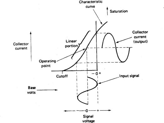
The main advantage of the class A amplifier is the relative lack of distortion. The output waveform follows that of the input waveform, except in amplified form. However, with any class of amplifier there is some distortion, as discussed in Section 1.8. The main disadvantages of class A are relative inefficiency (lower power output for a high-power input dissipated by the transistor) and the inability to handle large signals. Rarely is a class A amplifier over about 35% efficient.
The peak-to-peak output-signal voltage swing of a class A amplifier is limited to less than the total supply voltage. Because the output voltage must swing both positive and negative, peak output is less than half the supply voltage. The input voltage swing of class A is limited by the output voltage swing capability and the voltage-amplification factor. For example, if the output is limited to ±10 V and the voltage-amplification factor is 100, the input is limited to ±0.1 V (100 mV). Because of these limitations, class A amplifiers are generally used as voltage amplifiers rather than power amplifiers. Typically, a class A amplifier is used ahead of a power amplifier.
1.7.2 Class B Amplifier
As shown in Fig. 1-7, a class B amplifier operates only on half of the input signal. Class B operation is produced when the base-emitter bias is set so that the operating point coincides with the transistor cutoff point. For an NPN transistor, this means making the base more negative than for class A operation. (For PNP transistors, class B is produced when the base is more positive than for class A.) Either way, the base-emitter reverse bias is increased for class B operation.
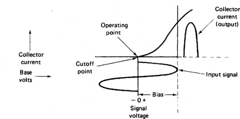
As shown in Fig. 1-7, when the input signal voltage is zero, there is no flow of collector current. During the positive half-cycle of the signal voltage, the collector current rises to the peak and then falls back to zero in step with the variations of that half-cycle. During the negative half-cycle, there is no collector current because the base-emitter reverse bias is always greater than the transistor cutoff voltage. Collector current flows only during half of the input-signal cycle.
There is considerable distortion if a single transistor is operated as class B because the waveform of the resulting collector current does not represent the complete waveform at the input. Class B is generally used when two transistors are connected in push-pull (where each transistor reproduces half of the input). All other factors being equal, it is possible to operate class B at a higher current (or power) rating than class A. As a result, class B amplifiers are generally used as power amplifiers rather than as voltage amplifiers.
1.7.3 Class AB Amplifier
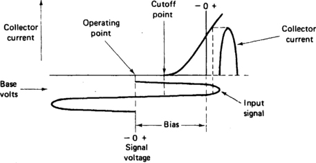
As shown in Fig. 1-8a, true class B operation often results in crossover distortion, because there is no collector-current flow when the base-emitter voltage is below about 0.65 V (for a silicon transistor). During the time when one transistor stops conducting and the other starts conducting, the output waveform is distorted. It is possible to minimize the effects of crossover distortion by operating the amplifier as class AB, where the transistors are forward biased just enough for a small amount of collector current to flow at the Q point. The combined collector currents produce a composite curve that is essentially linear at the crossover point, resulting in a faithful reproduction of the input, as shown in Fig. 1-8b.

1.7.4 Class C Amplifier
As shown in Fig. 1-9, the output of a class C amplifier is distorted from that of the input. Collector current flows only during a portion of the input signal between the cutoff point and the peak. The resulting collector current is a pulse, the duration of which is considerably less than a half-cycle of the input signal. As a result, the waveform of the output cannot resemble that of the input signal, nor can the output be restored by push-pull (as with class B or AB). Generally, class C is limited to those applications where distortion is of no concern (such as in RF amplifiers or video amplifiers in which square waves and pulses are involved).
1.8 Amplifier Distortion Basics
For the purposes of this book, distortion is defined as that condition when the output signal of an amplifier is not identical to the waveform of the input signal. The following paragraphs summarize some common problems. Intermodulation distortion and harmonic distortion are discussed in Chapter 2.
1.8.1 Amplitude Distortion Basics
Amplitude distortion occurs in the transistor and is the result of operating the transistor over the nonlinear portion of the characteristics curve (Fig. 1-6). The usual remedy is to use a bias that places the operating point well within the linear portion, preferably at the center of the linear portion. In addition, the amplitude of the input signal must be small enough so that the positive and negative half-cycles do not drive the transistor beyond the linear portion. Generally, a low input signal and proper operating point (at the center of the linear portion) mean that gain must be sacrificed. To sum up, an overdriven amplifier (used to get maximum gain) almost always results in some amplitude distortion. A low-distortion amplifier generally requires at least two stages to get the same gain as an overdriven amplifier.
1.8.2 Frequency Distortion Basics
Frequency distortion occurs because the input signal rarely, if ever, is at a single frequency. Instead, the input signal usually contains components of several frequencies, making the signal waveform somewhat complex. The amplifier circuit is composed of resistors, capacitors (unless direct coupled), and possibly inductances (coils/transformers). Capacitors and inductances have reactance. Because reactance is a function of frequency, the different signal frequencies produce different reactances and attenuate the signal by different amounts. This produces distortion of the signal waveform from the original.
1.8.3 Phase Distortion Basics
When a signal flows through a capacitance or inductance, the signal is shifted in phase. The degree of this shift is a function of frequency. Because several frequencies are present simultaneously, several phase shifts occur, producing phase distortion. As in the case of frequency distortion, amplifier phase distortion can be minimized by proper design.
1.9 Frequency Limitations in Amplifiers
Every electronic component has some impedance and is thus frequency sensitive. The component does not attenuate (or pass) signals of all frequencies equally. Even a simple length of wire has impedance. Wire, being a conductor, has some resistance. If alternating current is passed through the wire, there is some inductive reactance. If the wire is near another conductor (even PC wiring), there is some capacitance between the two conductors, and thus some capacitive reactance. The reactance and resistance combine to produce impedance which, in turn, varies with frequency. The following is a summary of the effect on amplifier performance caused by frequency limitations.
As shown in Fig. 1-10, all transistors have some capacitance between the junctions (emitter-base and collector-base). This applies to discrete transistors as well as transistors found in IC amplifiers. If any of the elements is common or ground, the remaining elements have some capacitance to ground. Capacitive reactance decreases with an increase in frequency, and vice versa. In the circuit shown in Fig. 1-10, the capacitive reactance drops as frequency increases, producing a short across the input and output. This attenuates the signal and, at some frequencies, the attenuation equals the transistor amplification, so there is no gain.
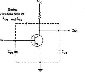
Figure 1-11 is a simplified frequency-response curve or graph for a typical amplifier. (More comprehensive graphs, as well as the procedures for producing such graphs, are discussed in Chapter 2.) The graph shown in Fig. 1-11 is provided here to illustrate the effects of transistor capacitance and coupling methods on amplifier frequency response. Note that the amplifier gain falls off at both the low- and high-frequency ends. The drop in gain (generally called rolloff) at the high end is caused by the transistor capacitance (as shown in Fig. 1-10).

Figure 1-12 shows the effect on amplifier frequency range of coupling capacitors used at the input and output of amplifier stages (to block direct current). The values of such coupling capacitors determine the low-frequency limits of the amplifier circuits. In effect, C1 forms a high-pass (or low-cut) filter with resistor RB, and capacitor C2 forms another low-cut filter with the input resistance of the following stage (or the load).

Input voltage to the low-cut filters is applied across the capacitor and resistor in series. The filter output voltage is taken across the resistance. The relationship of input voltage to output voltage is output voltage = input voltage × (R/Z), where R is the d-c resistance value and Z is the impedance (obtained by the vector combination of series capacitive reactance and d-c resistance).
When the reactance of C1 and/or C2 is about half the corresponding resistance, the output drops to about 90% of the input (or about a 1-dB loss). Using the 1-dB loss as the low-frequency cutoff point, the approximate value of C1 or C2 can be found by capacitance = 1/(3.2 F R), where capacitance is in farads, F is the low-frequency limit in Hz, and R is resistance in ohms. If a 3-dB loss at the low-frequency cutoff point be tolerated, the value of C1 or C2 can be found by capacitance = 1/(6.2 F R).
1.10 Coupling Methods
Figure 1-13 shows the classic coupling methods used in amplifier circuits. All amplifiers require some form of coupling. Even a single-stage amplifier must be coupled to the input and output devices. If more than one stage is involved (as is the case in virtually all IC amplifiers), there must be interstage coupling. The coupling methods shown in Fig. 1-13 require resistance and could be called resistance-coupled. However, the term “resistance-coupled” is generally used to indicate that the amplifier does not have inductances or transformers between stages and that the input and/or output impedance is formed by a resistance. Capacitor coupling is often called “resistance-capacitance (or RC) coupling.”
Most IC amplifiers use only direct coupling. One reason for this is because capacitors are difficult to fabricate in IC form. The other reason is that with direct coupling it is possible to amplify direct-current signals (or level shifts) and very low-frequency signals.
1.11 FET Amplifier Basics
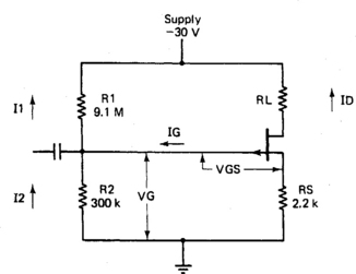
Figure 1-14 shows a basic FET bias circuit. The characteristics of FETs are quite different from those of bipolar transistors. This results in considerable differences in amplifier characteristics. Figure 1-15 summarizes some of these differences.
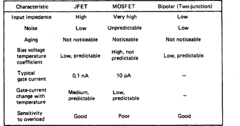
As shown, the FET has several advantages over a bipolar transistor in amplifier applications. The FET is relatively free of noise and is more resistant to the degrading effects of nuclear radiation. The FET is also inherently more resistant to burnout than the bipolar transistor. The high input impedance (typically several megohms) is very useful when the amplifier must be matched to a high-impedance signal source. Because the FET is a voltage-controlled device, in contrast to current-controlled bipolar transistors, the FET can readily be self-biased. When compared with bipolar transistors, the major shortcoming of the FET is a relatively small gain-bandwidth product.
Two types of FETs are commonly used in IC amplifiers, junction (JFET) and metal oxide semiconductor or silicon (MOSFET). As the names imply, JFET uses the characteristics of a reverse-biased junction to control the drain-source current (ID of Fig. 1-14), whereas with a MOSFET the gate is a metal deposit on an oxide layer. The gate is insulated from the source and drain. Because of this insulated gate, the MOSFET is sometime called an insulated-gate FET, or IGFET (but the term “MOSFET” is in more common use).
Both MOSFETs and JFETs operate on the principle of a channel current controlled by an electric field. The control mechanisms for the two are different, resulting in considerably different amplification characteristics. The main difference in the two (from a simplified-design standpoint) is in the gate input characteristics. The input to a JFET amplifier acts like a reverse-biased diode, whereas the input of a MOSFET amplifier is similar to a small capacitor.
1.12 Multistage Amplifiers
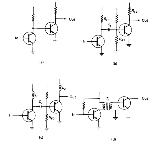
Virtually all IC amplifiers use direct-coupled multistage circuits. When stable voltage gains greater than about 20 are required, two or more transistor-amplifier stages can be used in cascade (where the output of one transistor is fed to the input of a second transistor). In theory, any number of amplifiers or stages can be connected in cascade to increase voltage gain. In practice, the number of stages is usually limited to three. The overall gain of the amplifier is equal (approximately) to the cumulative gain of each stage, multiplied by the gain of the adjacent stage. For example, if each stage in a three-stage amplifier has a gain of 10, the overall gain is (approximately) 1,000 (10 × 10 × 10). The following is a summary of some classic multistage direct-coupled amplifiers. Although these circuits are in discrete form, corresponding circuits are found in IC form.
1.12.1 Direct-Coupled Complementary Amplifier
Figure 1-16 shows a direct-coupled complementary amplifier where Q1 is an NPN transistor with the collector coupled directly to the base of Q2, a PNP transistor. The forward bias for the emitter-base junction of Q1 and the reverse bias for the collector-base junction are taken from the +VCC supply. The emitter of Q2 is connected to +VCC through RE2 (which is bypassed by CE2). The collector resistor RL1, the impedance of Q1, and resistor RE1 form a voltage divider across the VCC supply. (In a typical IC amplifier circuit, capacitors CE1 and CE2 would not be used.) The base of Q2 is less positive (or more negative) than the emitter. Thus, the emitter-base junction of Q2(PNP) is forward biased. The collector of Q2 is grounded through the output load resistor RL2. Because the negative terminal of the power supply (–VCC) is also grounded, reverse bias for the collector-base junction of Q2 is established.
1.12.2 Three-Stage Complementary Amplifier
Figure 1-17 shows a three-stage complementary amplifier. Note that the increased stabilization for any complementary amplifier occurs because any change in collector current (because of temperature, power-supply variation, etc) is opposed by an equal change in collector current for the following stage. Of course, NPN and PNP stages must be used alternately, as shown.

1.12.3 Direct Coupling Between Unlike Stages
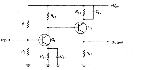
Figure 1-18 shows how to use direct coupling between unlike stages (between a common-emitter amplifier and an emitter follower, in this case). Here, the collector of Q1 is direct coupled to the base of Q2, which is connected as a common-collector (emitter-follower). Forward bias for the emitter-base junction of Q2 is taken from the power supply through RL, which also serves as the collector load for Q1. Output is taken across RE2, which is the emitter resistor for Q2. This circuit is particularly useful when the output must be at a low impedance. The value of RE2 sets the approximate output impedance of the circuit.

1.12.4 Darlington Compound
Figure 1-19 shows the basic Darlington circuit (known as the Darlington compound) together with two practical versions of the circuit. The Darlington compound is an emitter follower (or common collector) driving a second emitter follower. The main reason for using a Darlington compound is to produce high current (and power gain). For example, Darlington compounds are often used to raise the power of a signal from a voltage amplifier to a level suitable to drive a final power amplifier.
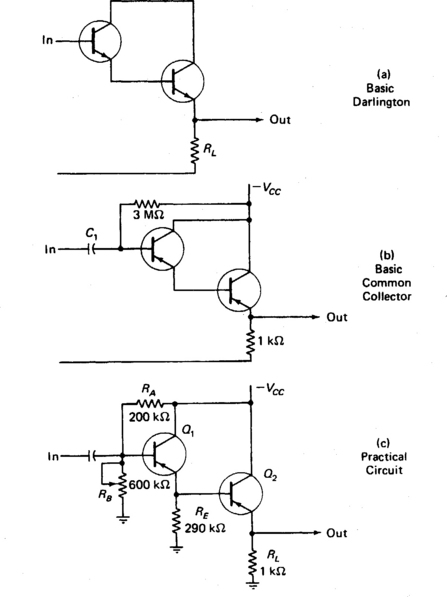
When the Darlington compound is used as a common collector, as shown in Fig. 1-19, the output impedance is about equal to the load resistance RL. The input impedance is approximately equal to beta2 × RL. The current gain is about equal to the average beta of the two transistors, squared. However, from a simplified-design standpoint, power gain is the primary reason for using a Darlington compound.
1.13 Bipolar/FET Direct-Coupled Amplifiers
In certain applications, bipolar transistors and FETs are combined in a single IC to form amplifier circuits. The classic example is where FET stages are used at the input, followed by bipolar stages. Such an arrangement takes advantage of both the FET and bipolar transistor characteristics.
An FET is essentially a voltage-operated device, permitting large voltage swings with low currents. This makes it possible to use high resistance values (resulting in high impedances) at the input and between stages. In turn, these high resistance values permit use of low-value coupling capacitors (if required). When an FET is used as the input stage, the amplifier input impedance is high. This places a small load on the signal source.
Bipolar transistors are essentially current-operated devices, permitting large currents at about the same voltage levels as the FET. Thus, with equal supply voltages and signal-voltage swings, the bipolar transistor can supply much more current gain (and power gain) than the FET. Because currents are high, bipolar transistor impedances are low, thus providing a low output impedance when the final amplifier stages are bipolar.
1.13.1 Typical Bipolar/FET Direct-Coupled Amplifier
Figure 1-20 shows a direct-coupled amplifier using a JFET input stage and a bipolar transistor pair as the output. Note that local feedback is used in the FET stage (provided by RS), as well as overall feedback (provided by R4). Input impedance is set by the value of R2. Output impedance is set by the combination of R4 and RS. However, because RS is quite small in comparison to R4, the output impedance is essentially equal to R4.

1.13.2 Nonblocking Bipolar/FET Direct-Coupled Amplifier
Figure 1-21 shows a nonblocking bipolar/MOSFET direct-coupled amplifier. Generally, a direct-coupled amplifier does not require any coupling capacitors. One exception is a coupling capacitor at the input to isolate the amplifier from direct current (when the signal is composed of both direct current and alternating current). When a coupling capacitor is used at the gate of a JFET, a condition known as blocking occurs.

Blocking occurs because the gate junction of a JFET is similar to that of a diode. This simulated “diode” acts to rectify the incoming signal. If a capacitor is connected in series with the diode (gate junction), large signals can charge the capacitor. On one half-cycle, the diode is forward biased and charges rapidly. On the opposite half-cycle, the diode is reverse biased and discharges slowly. If the signal and charge are large enough, the amplifier can be biased at or beyond cutoff until the capacitor discharges. Thus, the amplifier can be blocked to incoming signals for a period of time.
One method of eliminating the blocking problem is to use a MOSFET at the input, as shown in Fig. 1-21. Because the gate of a MOSFET acts essentially as a capacitor (rather than a diode), there is no rectification of the signal and no blocking occurs.
1.14 Chopper Stabilization
A major problem with any direct-coupled amplifier is that the circuit responds the same way to a change in power-supply voltage as to a change in the d-c signal level. This effect can be minimized by feedback, temperature-compensating diodes, and complementary circuits (see Section 1.12.2). However, none of these methods can compensate for a constantly changing or drifting power supply (from whatever cause) when the signal is also direct current.
One method for overcoming the voltage-change problems of direct-coupled amplifiers is to convert the d-c signal to an equivalent a-c signal (through modulation). The a-c signal is amplified in a gain-stabilized a-c amplifier and then reconverted to direct current (through demodulation). During amplification, the signal is not affected by drift. Such a system is shown in Fig. 1-22 where the amplifier input is switched alternately to both sides of a transformer. This periodically inverts the polarity of the signal applied to the amplifier, thus converting d-c to a-c. Note that although mechanical switches are shown in Fig. 1-22, the switching system is solid-state for present-day IC amplifiers.

In the circuit shown in Fig. 1-22, a second pair of contacts at the output establishes the ground level for a storage capacitor in series with the output. The output storage capacitor becomes charged to a level corresponding to the amplitude of the output square wave. Synchronous detection preserves the polarity of the input voltage and recovers both positive and negative voltages with the correct polarity. The synchronous modulation and demodulation is known as chopping or chopper stabilization. A direct-coupled amplifier with a chopper circuit offers drift-free amplification of low-level signals in the microvolt region.
One problem with chopper stabilization is frequency response. If the input is pure direct current, there is no problem. However, if the input is very low-frequency alternating current, the chopper frequency must be higher than the signal frequency. If not, the input signal waveform can be distorted or completely lost. For example, if both the input signal and chopping frequency are 100 Hz, and if the amplifier input is shorted at the same instant as the positive swing of the input signal, the amplifier sees only the negative portion of the input.
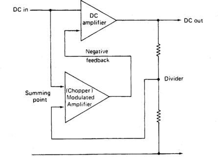
Figure 1-23 shows another method of chopper stabilization. Here, a chopper-modulated amplifier is used to correct the direct-coupled amplifier for voltage change or drift. Note that the input-signal direct current is amplified through a conventional d-c amplifier. A portion of the amplified output is tapped off from a divider network and compared with the original input signal. The divider network reduces the output by the same amount that is amplified by the d-c amplifier. Thus, the divider output should be equal to the input level at the summing point. Any difference at the summing point (caused by voltage change, drift, etc) is amplified through the modulated amplifier and then applied to the main-channel d-c amplifier as negative feedback to cancel the drift.
1.15 Differential Amplifiers
Figure 1-24 shows a basic differential amplifier. Figure 1-25 shows a more practical differential amplifier (typical of the circuits found in IC form). In both cases, the output signals are the result of a signal difference between two inputs. In theory, no output is produced by a differential amplifier when the input signals are identical. An output is produced only when there is a difference in input signals.

The two most common uses for differential amplifiers are as the input circuit for an operational amplifier or op-amp (see Chapter 3) and as an amplifier for laboratory meters, oscilloscopes, and recorders. Such instruments are operated in areas where many signals may be radiated (power-line radiation, stray signals from generators, and the like). Test leads connected to the input terminals pick up these radiated signals, even when the leads are shielded.
If a single-ended (nondifferential) input is used, the undesired signals are picked up and amplified along with the desired signal input. With a differential input, both leads pick up the same radiated signal at the same time. Because there is no difference between the radiated signals at the two inputs, there is no amplification of the undesired inputs.
Signals common to both inputs (such as radiated signals) are known as common-mode signals. The ability of a differential amplifier to prevent conversion of a common-mode signal into a difference signal (which produces an output) is expressed as the common-mode rejection ratio (CMR or CMRR). In the circuit shown in Fig. 1-24, a common-mode signal drives both bases in phase with equal-amplitude a-c voltages, and the circuit acts as though the transistors are in parallel to cancel the output. In effect, one transistor cancels the other.
Non-common-mode signals are applied to either of the bases (Q1 or Q2). The inverting input is applied to the base of Q2 and the noninverting input is applied to the base of Q1. With a signal applied only to the inverting input, and with the non-inverting input grounded, the output is an amplified and inverted version of the input. For example, if the input is a positive pulse, the output is a negative pulse. If the noninverting input is used with the inverting input grounded, the output is an amplified version of the input (but without inversion). The emitter resistor introduces emitter feedback to both transistors simultaneously. This reduces the common-mode signal gain without reducing the differential-signal gain in the same proportion.
1.15.1 IC Differential Amplifier
The circuit shown in Fig, 1-25 is basically a single-stage differential amplifier (Q2 and Q4) with input emitter followers (Q1 and Q5) and constant-current source Q3 in the emitter-coupled leg. Note that the single emitter resistor of Fig. 1-24 circuit is replaced by Q3 in the circuit of Fig. 1-25 and that direct coupling is used throughout the IC circuits.
The use of a transistor such as Q3 is typical for IC differential circuits (especially those found as the first stage in an op-amp). The circuit of Q3 is known as a temperature-compensated constant-current source. All current for the differential amplifier is fed through Q3 connected between the emitters of the differential amplifier and the negative power supply (VEE).
If there is an increase in current, a larger voltage is developed across Q3. This larger current acts to reverse bias the base/emitter junction, thus reducing current through Q3. Because all current for the differential amplifier is passed through Q3, current to the amplifier is also reduced. If there is a decrease in current, the opposite occurs, and the amplifier current increases. Thus, the differential amplifier is maintained at a constant current level.
Transistor Q3 is also temperature compensated by the diodes connected in the base-emitter bias network. These diodes have the same (approximate) temperature characteristics as the base-emitter junction and offset any change in Q3 base-emitter current flow that results from temperature change. The feedback resistors R4 and R5 increase linearity of the circuit. The output impedance between each output (terminals 8 and 10) and ground is essentially the value of the collector resistor R1 and R2 in the differential stage.
1.15.2 Common-Mode Definitions
The terms common-mode and common-mode rejection are used frequently in differential-amplifier applications. All manufacturers do not agree on the exact definition of common-mode rejection. For example, one manufacturer defines CMR (sometimes listed as CMrej) or CMRR as the ratio of differential gain (usually large) to common-mode gain (usually a fraction). That is, an amplifier may have a large gain of differential signals (different signals at each input terminal, or one input terminal grounded and the opposite input terminal with a signal), but little gain (possibly a loss) of common-mode signals (same signals at both terminals).
Another manufacturer defines CMR as the relationship of change in the output voltage to the change in the input common-mode voltage producing the change, divided by the open-loop gain (amplifier gain without feedback). For example, using the latter definition, assume that the common-mode input (applied to both terminals simultaneously) is 1 V, the resultant output is 1 mV, and the open-loop gain is 100. The CMR is then (output/input)/open-loop gain, or (0.001/1)/100 = 0.00001. This can be expressed as a CMR of 100,000 (or 100 dB).
Another method to calculate CMR is to divide the output signal by the open-loop gain to find an equivalent differential input signal. Then the common-mode input signal is divided by this equivalent differential input signal. Using the same figures as in the previous CMR calculation: 0.001/100 = 0.00001, equivalent differential input signal; 1/0.00001 = 100,000, or 100 dB.
No matter what basis is used for calculation, CMR is an indication of the degree of circuit unbalance in the differential stages because a common-mode input signal should be amplified identically in both halves of the circuit. A large common-mode output for a given common-mode input indicates a large imbalance (poor CMR). As with amplifier gain, CMR usually decreases (imbalance increases) when frequency increases.
1.15.3 Floating Inputs
Because a differential amplifier is sensitive only to the difference between two input signals (in theory), the signal source need not be grounded and can be floating. As a result, differential amplifiers are often used in test-equipment applications where the signal source is from a bridge (such as a bridge-type transducer) and the power supply is grounded. The differential amplifier also allows injection of a fixed d-c voltage into either channel to permit establishment of a new voltage reference level at the output (some point other than 0 V). This is sometimes known as zero suppression.
A floating-input circuit can create problems. When the input is floating, cable shielding between the amplifier and signal source may be connected to PC-board ground rather than to signal ground. However, both AC and DC voltages can exist between two widely separated earth grounds, causing current to flow. Such currents are known as ground currents, and the circuits producing the current flow are known as ground loops.
1.15.4 Basic Ground-Current Condition
Figure 1-26 shows the basic ground-current condition (where a bridge-type transducer is used with a differential amplifier, in this example). The signal source is connected to the transducer earth ground (local ground or physical ground). This ground point is connected to the amplifier ground through the cable shielding. The amplifier ground is connected to one of the differential inputs through the internal capacitance (represented as Cd) of the amplifier, even though there may be no d-c connection between ground and the input terminal of a floating-input amplifier.

The same differential input terminal is connected to the signal source through the signal leads and the transducer elements (bridge resistors, in this example). As a result, the a-c ground currents are mixed with the signal currents. This can produce an imbalance of the differential amplifier. In addition, radiated signals picked up by the shield appear as undesired differential signals rather than common-mode signals, and produce an undesired output.
1.15.5 Typical IC Differential Amplifier
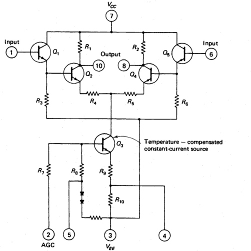
Figure 1-27 shows a differential amplifier in IC form. Transistors Q2 and Q4 amplify (differentially) the input signal applied between pins 9 and 10. The emitter-follower input buffering, provided by Q1 at the noninverting input and Q3 at the inverting input, is used to get the high input impedance needed to minimize the input capacitance and reduce the dependence of offset and impedance variations on device current gains.
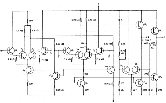
Transistor Q5 serves as a temperature-compensated current source, used primarily to provide a high common-mode rejection ratio. A common-mode feedback loop is incorporated around the input stage to provide Q-point operating stability for the input devices, and thus ensure a more predictable input common-mode voltage swing. The base of Q7 and collector of Q8 are bonded to pins 1 and 7 (as are the base of Q9 and collector of C10 to pins 2 and 6) to provide for open-loop frequency compensation capacitors (see Chapter 3) or for external adjustment controls.
A resistive level shifter follows the input stage to maintain the desired voltage levels at the overall IC output. (Level shifters are discussed further in Section 1.15.8.) The second differential-gain stage also contains emitter-follower buffering to minimize losses in the resistive level shifter and loading of the first-stage collectors.
Low output impedance and large output swing are provided at the output by differential emitter followers Q15/Q17. To improve peak negative swing of the amplifier, a current source Q18 (rather than an emitter resistor) is used to bias the emitter follower.
Stabilization of the output Q point is obtained by a local common-mode feedback loop incorporating a separate differential amplifier stage Q13/Q14. This circuit holds average-voltage output at ground potential (for split-supply operation) and at VCC/2 (for single power-supply operation). Changes in output Q point (no-signal drift) are minimized by temperature-compensation diodes D2/D3 in the base circuits of the feedback differential amplifier.
1.15.6 Differential Amplifiers as IC Op-Amps
The most common type of IC op-amp uses a balanced differential-amplifier circuit, such as shown in Fig. 1-28. The basic purpose of such a circuit is to produce an output signal that is linearly proportional to the difference between two signals applied at the input. The circuit shown provide an overall open-loop gain of about 2,500. In a theoretical differential amplifier, no output is produced when the signals at the inputs are identical, so differential amplifiers are particularly used for op-amps (common-mode signals are eliminated or greatly reduced).
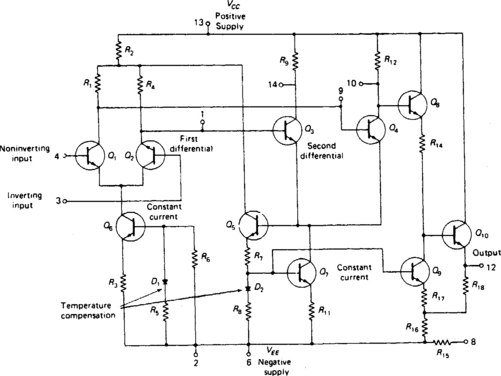
1.15.7 Typical IC Op-Amp Circuit
As shown in Fig. 1-28, the op-amp consists basically of two differential amplifiers and a single-ended output circuit in cascade. The pair of cascaded differential amplifiers provides most of the gain. The inputs to the op-amp are applied to the bases of emitter-coupled transistors Q1 and Q2 in the differential amplifier. With the non-inverting input grounded and signals applied only to the inverting input, the output is an amplified and inverted version of the input. For example, if the input is a positive pulse, the output is a negative pulse. If the noninverting input is used with the inverting input grounded, the output is an amplified version of the input (without inversion). Transistors Q1 and Q2 develop driving signals for the second differential amplifier.
Transistor Q6, a constant-current source, is included in the first differential stage to provide bias stabilization for Q1 and Q2. If there is an increase in supply voltage (which normally increases the current through Q1/Q2), the reverse bias on Q6 increases. This reduces the Q1/Q2 current and offsets the effect of the initial supply-voltage increases.
Diode D1 provides thermal compensation for the first differential stage. If there is an increase in operating temperature of the IC (which normally increases current through Q1/Q2), there is a corresponding current flow through D1, because the diode is fabricated on the same silicon chip as the transistors. The increase in D1 current also increases the reverse bias of Q6, thus offsetting the initial change in temperature.
The emitter-coupled transistors Q3 and Q4 in the second differential amplifier are driven push-pull by the outputs from the first differential amplifier. Bias stabilization for the second differential amplifier is provided by current transistor Q7. Compensating diode D2 provides thermal stabilization for the second differential amplifier and also for the current transistor Q9 in the output stage.
Transistor Q5 develops negative feedback to reduce common-mode error signals that are developed in the emitters of transistors Q3/Q4. Because the second differential-amplifier stage is driven push-pull, the signal at this point (the emitters) is zero when the first differential-amplifier stage and the base-emitter circuits of the second stage are matched, and there is no common-mode input.
A portion of any common-mode, or error, signal that appears at the emitters of transistors Q3/Q4 is developed by transistor Q5 across resistor R2 (the common-collector resistor for transistors Q1, Q2, and Q5) in the proper phase to reduce the error. The emitter circuit of transistor Q5 also reflects a portion of the same error signal into current transistor Q7 in the second differential stage so that the initial error signal is further reduced.
Transistor Q5 also develops feedback signals to compensate for common-mode effects produced by variations in the supply voltage. For example, assume a decrease in the voltage at the emitters of Q3/Q4. This negative-going change in voltage is reflected by the emitter circuit of Q5 to the bases of current transistors Q7/Q9. Less current then flows through these transistors.
The decrease in collector current of Q7 results in a reduction of the current through Q3/Q4, and the collector voltages of these transistors tend to increase. This tendency partially cancels the decrease that occurs with the reduction of the positive supply voltage.
The partially canceled decrease in collector voltage of Q4 is coupled directly to the base of Q8 and is transmitted by the emitter of Q8 to the base of Q10. At this point, the decrease in voltage is further canceled by the increase in the collector voltage of Q9. Because of the feedback stabilization provided by Q5, the IC op-amp has high common-mode rejection, excellent open-loop stability, and low sensitivity to power-supply variations.
The output from the op-amp is taken from the emitter of Q10 so that the d-c level of the output signal is substantially lower than that of the differential-amplifier output at the collector of Q4. In this way, the circuit shifts the output d-c level to the same level as the input (when no signal is applied).
1.15.8 DC Level-Shifting Problems
In any cascade direct-coupled amplifier, the d-c level rises through successive stages toward the supply voltage. In linear ICs, the d-c voltage builds up through the NPN stages in the positive direction and must be shifted in the negative direction if large output-signal swings are required. For example, if the supply voltage is 10 V and the output is at 9 V under no-signal conditions, the maximum output voltage swing is limited to less than 1 V.
With multi-stage high-gain ICs, such as op-amps or any circuit that uses external feedback, it is especially important to provide for compensation of the d-c level shift. Such amplifiers must have equal (and preferably zero) input and output d-c levels so that the d-c coupling of the feedback connection does not shift any bias point. For example, if the input is at 0 V but the output is at 3 V, this 3 V is reflected back through an external feedback resistor and changes the input to a 3-V level.
The use of an output stage, such as shown in Fig. 1-28, is a common technique for preventing a d-c level shift between the output and input of an IC. Transistor Q8 operates as an input buffer, and transistor Q9 is essentially a current sink for Q8. The shift in d-c level is done by the voltage drop across R14 (produced by the collector current of Q9). Feedback through R18 results in a decrease of the voltage drop across R14 for negative-going output swings and an increase for positive-going output swings.
The circuit of Fig. 1-28 provides many connections to internal circuit components. For example, feedback may be coupled from the output to the input to stabilize gain (or to compensate for common-mode effects that result from variations in supply voltage). Also, the additional connections (such as at the collectors of Q1, Q2, Q3, Q4, and Q9) provide a variety of input/output points for the phase-lead and phase-lag compensation techniques described in Chapter 3.