
Audiofrequency Amplifier Design
This chapter is devoted to simplified design with audiofrequency (AF) ICs. Although such ICs are used primarily for consumer electronics, they can be adapted to any application where a number of AF amplifier functions are available in a single IC. Also note that the ICs discussed here are not necessarily limited to AF operation.
8.1 Low-Distortion Wideband Power Op-Amp
Figures 8-1 and 8-2 show the circuit schematic and performance characteristics, respectively, for a classic power op-amp (the National Semiconductor LH0101). This device has a gain bandwidth of 4 MHz and an output current of 2 A, and includes circuits to eliminate the crossover distortion discussed in Section 1.7.3. This IC has long been used when a high-current, low-distortion output is required in a single package.
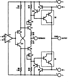
FIGURE 8-1 Power op-amp schematic (National Semiconductor, Linear Applications Handbook, 1994, p. 619)
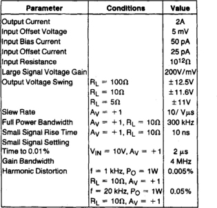
FIGURE 8-2 Power op-amp characteristics (National Semiconductor, Linear Applications Handbook, 1994, p. 618)
8.1.1 Power Amplifier Circuit
As shown in Fig. 8-1, the IC contains three stages: an op-amp, a buffer, and a power-output stage. The op-amp is used at the input to provide the usual differential input. The buffer stage, consisting of Q3, Q5, Q10, and Q11, is a current amplifier with unity voltage gain. Connected as a class AB amplifier, the buffer functions to provide distortion-free drive during zero crossing. (Buffer bandwidth is in excess of 50 MHz to ensure no bandwidth-induced distortion.)
The buffer output is currently limited by Q7/Q8 to no more than 50 mA. However, the power-stage Darlington transistors Q1/Q2 are designed to turn on when the load current reaches about 25 mA. Any additional current demand is sustained by Q1/Q2 up to the rated output load. The reserve drive of the buffer stage is used to smooth the turn-on delay of Q1/Q2, thus providing protection against crossover distortion.
Transistors Q6 and Q9 function as current-sense devices to protect the output stages. Current-sense resistors are connected between the supply pins and the SC pins (1 and 8) to program the limit threshold. An approximate 0.6-V differential at the base-emitter junctions of Q6/Q9 turns these transistors on. When Q6/Q9 are turned on, transistors Q4/Q12 are driven into conduction to draw off excess base current from the output Darlingtons Q1/Q2, and thus prevent the output stages from operating too high a current.
8.1.2 Crossover Distortion Performance
Figures 8-3, 8-4, and 8-5 show the crossover-distortion performance in the presence of both small-signal and large-signal inputs.
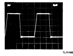
FIGURE 8-3 Power op-amp large-signal pulse response (National Semiconductor, Linear Applications Handbook, 1994, p. 620)

FIGURE 8-4 Power op-amp small-signal sine-wave response (National Semiconductor, Linear Applications Handbook, 1994, p. 620)

FIGURE 8-5 Power op-amp small-signal triangular-wave response (National Semiconductor, Linear Applications Handbook, 1994, p. 620)
Figure 8-3 shows the response to a large-signal input pulse when the IC is driving a 10-ohm load. As shown, there is no noticeable crossover distortion.
Figure 8-4 shows the response to a small-signal sine-wave input pulse when the IC is driving a 10-ohm load. Again, there is no crossover distortion at the zero-crossing point.
Figure 8-5 shows the response to a small-signal triangular input when the IC is driving a 1-ohm load (very heavy current!). Notice that there is a slight indication of crossover distortion at the zero-crossing point, but very little considering the output current.
8.1.3 Circuit Layout Considerations
As is the case with any power application, it is always necessary to pay close attention to the PC trace connections in which high current is carried. Critical connections should be short to minimize voltage drop on the trace. For example, a 10-milliohm PC trace carrying 2 A develops a 20-mV error voltage. It is important to be aware of where this error is generated and how the error affects circuit accuracy.
Ground connections are probably the most important, if not the most troublesome. Not only can grounds contribute to circuit error, but (in many situations) the circuit can become unstable if the layout produces excessive phase shift. Figure 8-6 shows one correct technique for circuit grounding. The heavy lines represent high-current paths. Note that the signal ground is also returned to the supply ground.

8.1.4 Limiting Output Current
Figure 8-7 shows current-sense resistors (RSC) connected between the supply and the SC terminals to limit output current. As discussed, when 0.6 V is developed across these resistors, the output-limiting circuit is triggered. Figure 8-7 also shows the equation for calculating the correct values of the RSC resistors for a specific output-current limit (ISC).

FIGURE 8-7 Current-limit protection (National Semiconductor, Linear Applications Handbook, 1994, p. 621)
Because of the currents involved, it is quite possible that the RSC resistors will be less than 1 ohm. This brings up a possible problem with solder connections and socket contacts. The resistances from such connections and contacts become important and must not be overlooked. Even a good solder joint can show 5 milliohms of resistance. Typical socket contacts have about 10 milliohms. Even the resistances of interconnecting traces can become significant if the traces are long.
For example, in the circuit shown in Fig. 8-7, the pair of solder joints at each end of the 0.3-ohm RSC contributes more than 3% error. Add this to a possible 10% variation in current-sense transistor threshold and a temperature coefficient of −2 mV/°C for the threshold, and you have a 20% to 25% accuracy for the current limit. As a result, when designing the current limit, do not set the limit too close to the worst-case peak current under any normal operating conditions.
If the threshold is intermittently exceeded, even for a very short time, the signal can be distorted. In the worst case, the circuit can be triggered into oscillation, particularly when the circuit is driving a capacitive load (Section 8.8). (Such distortion and oscillation can occur in other op-amps having similar current-sense circuits.) Although the current-limit circuit has enough gain to produce a sharp response if the limit is exceeded, allow a 20% margin above the worst-case operating condition.
8.1.5 Safe Operating Areas
Figure 8-8 is reproduced from the data sheet and shows the safe operating areas, both with and without heat sinks. Do not operate the IC beyond the boundaries defined in Fig. 8-8! For example, if the output voltage is 10 V, the absolute maximum output current is something less than 1 A if the IC is operated without a heat sink and with an ambient temperature of 25°C.

8.1.6 Power-Derating Curves
Figure 8-9 is reproduced from the data sheet and shows the power-derating factors, again both with and without heat sinks. Do not operate the IC beyond the boundaries defined in Fig. 8-9. For example, if the ambient temperature is 25°C and the IC is operated without a heat sink, the maximum permitted power dissipation is about 5 W. If the ambient temperature is increased to 75°C and the IC is operated without a heat sink, the maximum permitted power dissipation is reduced to about 2 or 3 W.

8.1.7 Heat Sink Calculations
As discussed in Section 1.5.5, heat sinks are not covered in this book because most of the IC described are voltage amplifiers rather than power amplifiers. However, the following paragraphs summarize the calculations for heat sinks as they apply to this particular IC amplifier.
Note that both the safe-operating (Fig. 8-8) and power-derating (Fig. 8-9) curves assume that the heat sink is infinite. That is, the thermal resistance RØ is zero and the heat sink will dissipate all heat. Unfortunately, heat sinks have some thermal resistance from the sink to ambient air RØSA. This must be added to the thermal resistance of the IC from the junction to case RØJC. Both RØSA and RØJC are rated in terms of °C/W, indicating how much the temperature will rise for each watt of power dissipated. The smaller the °C/W figure, the more efficient the heat dissipation.
In addition, as shown in Fig. 8-6, the metal case of the IC (a TO-3 case) is electrically connected to the amplifier output. Unless the application permits direct mounting to a heat sink, insulating material must be placed between the case and sink to provide electrical insulation. The thermal resistance of the insulator material and any thermal-joint compound used between the case and sink (RØCS) must also be added to find the total °C/W figure.
When all three thermal-resistance factors are added (RØJC + RØCS + RØSA), the result is the total thermal resistance from junction to ambient and is a measure of how much the temperature will rise from the ambient for each watt dissipated by the IC.
To find the maximum permitted power dissipation for the IC, subtract the ambient from the maximum permitted junction temperature (150°C for the LH0101, and a safe figure for most silicon power ICs), and then divide by the total thermal resistance. For example, assume that the IC is to be operated at 25°C without a heat sink and that the junction to ambient RØJA is 30°C/W for the case. (This is a safer factor than the 25°C/W RØJA shown in Fig. 8-9.) Under these conditions, the maximum permitted power dissipation is
(150°C – 25°C)/30°C/W = 4.16 W.
This is about the same as shown in Fig. 8-9. Keep in mind that the power dissipation is a combination of load power and the quiescent power dissipated by IC circuits.
Now assume that the IC is operated at 25°C with a heat sink, that the sink has a RØSA of 3.5°C/W, that the IC RØJC is a safer 2.5°C/W (instead of the 2°C/W shown in Fig. 8-9), and that the total RØCS (insulator and thermal compound) is 0.5°C/W (a realistic figure). This produces a total junction to ambient RØJA of 6.5°C/W (2.5 + 0.5 + 3.5). Under these conditions, the maximum permitted power is (150°C – 25°C)/6.5°C/W = 19.23 W. This is a far more realistic figure than the infinite heat sink values shown in Figs. 8-8 and 8-9.
8.1.8 Driving Inductive Loads
The IC is suitable for driving most inductive loads, including speaker voice-coils and motors. However, in some applications, the IC should be protected from the harmful effects of energy stored in the inductor. Such a condition exists when power is removed from the circuit at an instant when a high current is flowing through the inductor. A back-emf may be large enough to forward bias internal junctions at a current sufficient to destroy the IC. Figure 8-10 shows a simple circuit (two diodes) to prevent this condition.

FIGURE 8-10 Driving inductive loads (National Semiconductor, Linear Applications Handbook, 1994, p. 622)
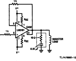
Another possible problem is loop instability and oscillation. In theory, an inductive load does not cause amplifier loop instability. However, if the circuit Q is high enough and stray capacitances are within a critical range, the load circuit can break into oscillation. As shown in Fig. 8-11, a series RC damping circuit of 10 ohms and 0.01 µF across the inductor usually eliminates any possible oscillation. In some applications where it is desirable to prevent power-on surges from actuating an inductive load (for example, a motor valve actuator or disk-drive read/write head servo loop), the same RC damping circuit provides an alternate conductive path to suppress surge current.
8.1.9 Driving Capacitive Loads
Capacitive loads tend to create an undesirable frequency response at the frequency where open-loop gain approaches unity gain. The result is a reduction of phase margin. For example, a 500-pF load capacitor reduces a no-load phase margin of 58° down to 45°. A 1,000-pF capacitor reduces the phase margin to 40°. If the capacitive load is increased to 0.01 µF, the phase margin is reduced to 22°, which could easily result in oscillation (Chapter 3).
Figure 8-12 shows a compensation technique to restore stability when the IC is used to drive capacitive loads. The value of capacitor C1 should be such that the capacitive reactance is one-fifth the resistance of R2 at the unity-gain crossover frequency of the IC (4 MHz). R1 and R2 set the closed-loop gain in the usual manner.

FIGURE 8-12 Driving capacitive loads (National Semiconductor, Linear Applications Handbook, 1994, p. 623)
Note that if the load capacitance is increased beyond a certain point, there is no need for C1. This is because the time constant is so large that the circuit cannot oscillate. The load-capacitance value for the IC is approximately 0.1 µF or larger. Any load capacitance greater than this should not require a compensation capacitor C1.
8.1.10 Low-Distortion 40-W Audio Amplifier
Figure 8-13 shows two LH0101 ICs connected to provide a low-distortion 40-W audio amplifier. Figure 8-14 shows the amplifier characteristics. Figure 8-15 shows the total harmonic distortion versus frequency for the circuit. The ICs are connected as a bridge amplifier to get maximum output power for a given set of supply voltages (18 V). The heat sink used is a Thermalloy type 6141, which is rated at 3°C/W to 5°C/W.

FIGURE 8-13 Bridge audio power amplifier (National Semiconductor, Linear Applications Handbook, 1994, p. 626)


8.2 Gated Linear Amplifier
Figures 8-16 and 8-17 show the circuit schematic and performance characteristics, respectively, for a gated linear amplifier (the GEC Plessey ZN424P). Figure 8-18 shows offset and frequency-compensation connections for the IC. The amplifier has both low noise and low distortion, making it suitable for audio-amplifier applications, with an output up to ±11 V. However, the IC can also operate at 5 V, making it suitable for digital work.

FIGURE 8-16 Gated linear amplifier schematic (GEC Plessey Semiconductors, Professional Products, 1991, p. 1–78)

FIGURE 8-17 Gated linear amplifier characteristics (GEC Plessey Semiconductors, Professional Products, 1991, p. 1–80)
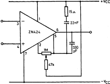
FIGURE 8-18 Gated linear amplifier offset/frequency compensation (GEC Plessey Semiconductors, Professional Products, 1991, p. 1–81)
8.2.1 Design Considerations
Although the characteristics given in Fig. 8-17 are based on a supply voltage of ±12 V, the IC will operate at supply voltages from ±2 V to ± 18 V over a temperature range of 0 to +70°C. The absolute maximum internal power dissipation is 250 mW. Maximum storage temperature is −65 to +125°C. Maximum differential input voltage is 5 V.
When operating with low supply voltages, the output bias current can be maintained at about 3 mA by connecting an external resistor between the gating input (pin 8) and +VCC. This disables the gating function and produces an output current approximately equal to
where R is the parallel combination of the external and internal (23-k) resistors.
Frequency stability at the maximum unity-gain frequency (1 MHz) is achieved by connecting a 22-nF capacitor and a 15-ohm resistor in series between the balance/shaping terminal (pin 5) and +VCC (pin 1), and a 330-pF capacitor between pin 5 and the output (pin 6), as shown in Fig. 8-18.
The input offset voltage is nulled by connecting a 1-M potentiometer between the balance/shaping terminal (pin 5) and the balance terminal (pin 2). As shown in Fig. 8-18, the potentiometer wiper is connected through a 47-k resistor to +VCC.
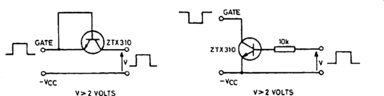
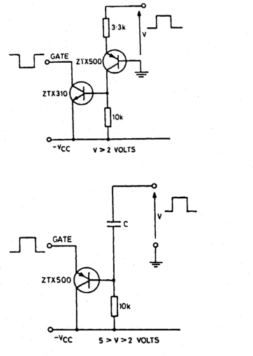
The IC is gated off by shunting the current-source bias current to the negative supply. Figures 8-19 and 8-20 show four methods for gating. The methods shown in Fig. 8-19 required a drive voltage that is referenced to –VCC. The drive pulse can be from another ZN424P or from logic when a single supply is used. The methods shown in Fig. 8-20 allow the drive pulse to be referenced from ground or other convenient point. When the IC is gated, the input-output coupling capacitance is about 1 pF.
8.2.2 Design Example
Figure 8-21 shows the IC connected in the basic noninverting unity-gain configuration. Direct feedback is accomplished by connecting output pin 6 to the inverting input pin 3 in the usual manner. The circuit can be converted to provide voltage gain by the addition of external components. Figure 8-22 shows the values for these external components to produce various amounts of closed-loop voltage gain.

FIGURE 8-21 Gating amplifier connected for noninverting unity gain (GEC Plessey Semiconductors, Professional Products, 1991, p. 1–83)
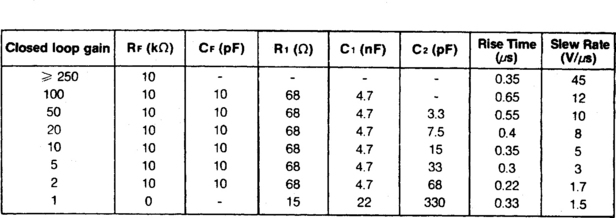
FIGURE 8-22 External component values for noninverting amplifier (GEC Plessey Semiconductors, Professional Products, 1991, p. 1–88)
Note that R1 and C1, referred to in Fig. 8-22, are connected in series between pins 1 and 5, as shown in Fig. 8-21. In addition, C2 is connected between pins 5 and 6. The values given in Fig. 8-22 should stabilize the circuit with less than 10% overshoot. The rise times and slew rates given in Fig. 8-22 are guidelines when the supply current is maintained at about 5 mA (by connecting an external resistor between pin 8 and +VCC, as described).
8.3 Ultra Low-Noise Preamplifier
Figures 8-23 and 8-24 show the internal circuits of an ultra low-noise preamplifier (the GEC Plessey SL561B/C). Figure 8-25 shows the electrical characteristics. The IC is designed as a high-gain, low-noise preamplifier for use in audio and video systems at frequencies up to 6 MHz. The noise performance is optimized for source impedances between 20 ohms and 1 k, making the device suitable for use with transducers (such as magnetic tape heads, photoconductive IR detectors, and dynamic microphones).

FIGURE 8-23 Internal functions of ultra low-noise preamplifier (TO-5 package) (GEC Plessey Semiconductors, Professional Products, 1991, p. 1–89)

FIGURE 8-24 Internal functions of ultra low-noise preamplifier (DIP package) (GEC Plessey Semiconductors, Professional Products, 1991, p. 1–89)

FIGURE 8-25 Electrical characteristics of ultra low-noise preamplifier (GEC Plessey Semiconductors, Professional Products, 1991, p. 1–90)
8.3.1 Design Considerations
The upper cutoff frequency or bandwidth of the amplifier can be reduced from 6 MHz to any desired value by a capacitor (C1) connected from pin 6 to ground, as shown in the typical applications schematic of Fig. 8-26. The cutoff frequencies for various values of C1 are shown in Fig. 8-27. Capacitor C1 does not degrade noise performance or output swing. As shown, the high-frequency rolloff is about 6 dB/octave. The characteristics shown in Fig. 8-27 are based on a VCC of 5 V, a source impedance of 50 ohms, a load impedance of 10 k, and an ambient temperature of 25°C using the test circuit shown in Fig. 8-28.
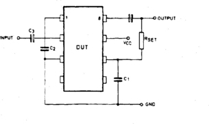
FIGURE 8-26 Ultra low-noise preamplifier application circuit (GEC Plessey Semiconductors, Professional Products, 1991, p. 1–89)
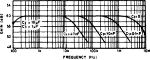
FIGURE 8-27 Gain/frequency characteristics (GEC Plessey Semiconductors, Professional Products, 1991, p. 1–91)

The low-frequency response is set by capacitors C2 and C3 (Figs. 8-26 and 8-27). Capacitor C2 decouples an internal feedback loop. If the value of C2 is close to that of C3, an increase in gain at low frequencies can occur. For a flat response, either make C2 0.05 µF less than C3 or make C2 5 µF greater than C3.
The voltage gain can be set by resistor RSET connected between pin 6 and the output. Figure 8-29 shows the values of RSET required to produce various voltage gains, from 10 to 60 dB. Note that certain minimum values of C1 are required for the voltage gains. This is because RSET increases the feedback around the output stage, and stability problems can result if the bandwidth is not reduced.
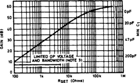
FIGURE 8-29 Values of RSET required to produce voltage gains (GEC Plessey Semiconductors, Professional Products, 1991, p. 1–91)
As shown in Fig. 8-30, the input stage is a common emitter without emitter degeneration (to improve the noise performance). When the voltage gain is set for less than 40 dB, the input stage (rather than the output) determines the maximum output voltage swing. For a distortion of less than 10%, the input voltage should be restricted to less than 5 mV, as shown in Fig. 8-31.

FIGURE 8-30 Ultra low-noise preamplifier schematic (GEC Plessey Semiconductors, Professional Products, 1991, p. 1–91)
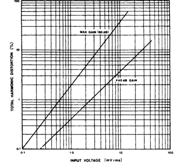
FIGURE 8-31 Ultra low-noise preamplifier THD (GEC Plessey Semiconductors, Professional Products, 1991, p. 1–92)
If larger voltage swings are required into low-impedance loads, the quiescent current of the output emitter-follower can be increased (from the normal 0.5 mA) by a resistor from pin 8 to ground. This resistor must not be less than 200 ohms to avoid exceeding current ratings of the output transistor.
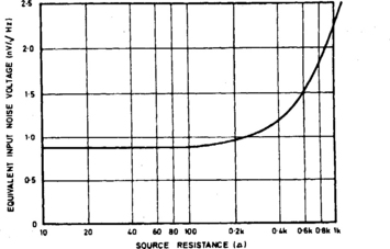
Figure 8-32 shows the equivalent input noise voltage for the amplifier. From this, the input noise voltage and current generators can be derived as follows: en = 0.8 nV/![]() In = 2.0 pA/
In = 2.0 pA/![]() So-called “flicker” or 1/f noise is not normally a problem.
So-called “flicker” or 1/f noise is not normally a problem.
8.4 No-Design Audio Amplifiers
This section is devoted to IC audio amplifiers that can be put to immediate use without design. These ICs are simply connected to power sources and turned on. Besides the input and output devices, the only external components required are coupling/decoupling capacitors and possibly volume controls. All the ICs are available from Philips Semiconductors.
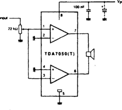
8.4.1 Stereo IC Audio Amplifier
Figure 8-33 shows a single IC connected to provide stereo amplification for low-power applications (small speakers or headphones). The circuit operates with battery supplies, from 6 V down to 1.6 V, and draws low quiescent current (typically 3.2 mA, with a 3-V supply). Closed-loop voltage gain is 26 dB with the connections shown. Output is 2 × 0.075 W with a 4.5-V supply, operating into 32-ohm loads. The output is reduced to 2 × 0.035 W when the supply is reduced to 3 V (with 32-ohm loads).

8.4.2 BTL IC Audio Amplifier
Figure 8-34 shows a single IC connected in the BTL (bridge-tied load) mode. This configuration provides low-voltage operation without sacrifice of output power (and is similar to the IC amplifier circuit shown in Fig. 8-13). The circuit seen in Fig. 8-34 operates with battery supplies from 6 V down to 1.6 V, and draws low quiescent current (typically 3.2 mA with 3-V supply). Closed-loop gain is 32 dB with the connections as shown (a floating differential input, 3-V supply, and 32-ohm load). The output is reduced to 0.14 W when the supply is reduced to 3 V (with a 32-ohm load).
8.4.3 BTL IC Audio Amplifier with Built-in Volume Control
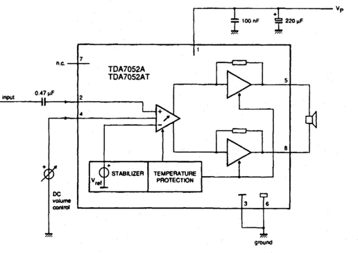
Figure 8-35 shows a single IC connected in the BTL mode, with a DC volume control. Again, this mode provides low-voltage operation without sacrifice of output power. The wide supply range (4.5 to 18 V) makes the circuit suitable for a broad range of applications (battery-powered radios, telephone sets, etc). The IC amplifier has a built-in DC volume control, with a log-characteristic range of more than 80 dB. When the DC control voltage (pin 4) drops below 0.3 V, the amplifier is muted so there are no switch-on/off clicks. The TDA7052A provides an output of 1 W, with a 6-V supply into an 8-ohm load, or 2-W output when the supply is raised to 12 V, into a 32-ohm load. The TDA7052AT output is 0.5 W with a 6-V supply, into a 16-ohm load. Both ICs include internal voltage-stabilization and temperature-protection circuits. The IC cuts off if the junction temperature reaches a level where there might be damage to the IC.
8.4.4 BTL IC Audio Amplifier with External Volume Control
Figure 8-36 shows a single IC connected in the BTL mode with an external volume control. This circuit is similar to that of Fig. 8-35, except that no built-in volume control is provided, so a conventional external AC volume control is needed. The supply range is from 3 to 18 V. The circuit provides an output of 1 W, with a 6-V supply, into an 8-ohm load, or 2-W output when the supply is raised to 11 V, into a 25-ohm load. Fixed, closed-loop voltage gain is 39 dB (6-V supply, 8-ohm load).

8.4.5 BTL Stereo IC Audio Amplifier
Figure 8-37 shows a single IC connected in the BTL mode to provide stereo amplification. The circuit has two conventional external AC volume controls, one for each stereo channel. The supply range is from 3 to 18 V. The circuit provides 1-W per channel output, with a 6-V supply, into 8-ohm stereo loads, or 2-W per channel output, with an 11-V supply, into 25-ohm loads. Fixed, closed-loop voltage gain is 39 dB (6-V supply, 8-ohm load).

8.4.6 BTL IC Audio Amplifier with 3.4-W Output
Figure 8-38 shows a single IC connected in the BTL mode with a built-in DC volume control. The circuit is similar to that of Fig. 8-35, except that the output is 3.4 W, with a 12-V supply, into a 16-ohm load.

8.4.7 BTL IC Audio Amplifier with 3-W Output
Figure 8-39 shows a single IC connected in the BTL mode with a conventional external AC volume control. The circuit is similar to that of Fig. 8-36, except that the output is 3 W, with an 11-V supply, into a 16-ohm load.

8.4.8 BTL Stereo IC Audio Amplifier with 3-W Output
Figure 8-40 shows a single IC connected in the BTL mode to provide stereo amplification. The circuit has two conventional external AC volume controls, one for each stereo channel. The supply range is from 3 to 18 V. The circuit provides 3-W per channel output, with an 11-V supply, into 16-ohm loads. Fixed, closed-loop voltage gain is 39 dB (11-V supply, 16-ohm loads).
