
Special-Purpose Amplifier Design
This chapter is devoted to simplified design with special-purpose IC amplifiers. These ICs (and the related application circuits shown here) are selected because they can be put to immediate use without design or with minimum design. The circuits are simply connected as shown and turned on. Besides the input and output devices, the only typical external components required are coupling/decoupling capacitors. When other external components are needed, values are provided for a given test result or design goal. This is supplemented with full information on how the external-component values affect the test/design results (so that other results can be obtained).
9.1 Gain-Controlled Microphone Preamplifier/VOGAD
Figures 9-1 and 9-2 show the circuit schematic and typical test/application diagram, respectively, for a microphone preamplifier/VOGAD with gain control (the GEC Plessey SL6270). This IC combines the functions of an audio amplifier and voice-operated gain-adjusting device (VOGAD). The IC is designed to accept signals from a low-sensitivity microphone and to produce an essentially-constant output signal over a 50-dB range of input signals. The dynamic range, frequency response, attack time, and decay time are all controlled by external components.

FIGURE 9-1 Gain-controlled microphone preamplifier/VOGAD (GEC Plessey, Professional Products, 1991, p. 1–146)
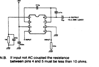
FIGURE 9-2 Gain-controlled microphone preamplifier/VOGAD test/applications (GEC Plessey, Professional Products, 1991, p. 1–147)
9.1.1 Input Characteristics
Input to the IC can be single-ended or differential, but must be capacitor coupled. In the single-ended mode, the signal can be applied to either input (pin 4 or pin 5), with the remaining input decoupled to ground as shown. Input signals of less than a few hundred microvolts are amplified normally. However, when the input level is increased, the AGC begins to take effect, and the output is held almost constant at 90 mV rms over an input range of 50 dB.
Both the dynamic range and sensitivity can be reduced by reducing the main-amplifier voltage gain. For example, if a 1-k resistor is connected between pins 7 and 8 (in parallel with the internal 10-k resistor), both the dynamic range and sensitivity are reduced by about 20 dB. (Values less than 680 ohms for the external resistor are not recommended.)
9.1.2 Frequency Response
Figure 9-3 shows the typical open-loop frequency response for the IC. Figure 9-4 shows how the closed-loop frequency response (bandwidth) and voltage gain can be set by external components.
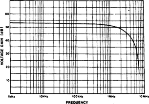
FIGURE 9-3 Typical open-loop frequency response (GEC Plessey, Professional Products, 1991, p. 1–148)

FIGURE 9-4 Setting closed-loop frequency response (GEC Plessey, Professional Products, 1991, p. 1–147)
The closed-loop voltage gain is set by the ratio of external feedback and input resistances in the usual manner.
The low-frequency response is set by the input, output, and coupling capacitors. In normal operation, the coupling capacitor between pins 2 and 7 (that passes the signal between the internal preamp and main amplifiers) is set at 2.2 µF to provide a −3 dB point at 300 Hz.
The high-frequency response is set by a capacitor in parallel with the feedback resistance. In normal operation, the capacitor between pins 7 and 8 is set at 4.7 nF to provide an upper frequency limit of 3 kHz.
With the values as shown in Fig. 9-4, the voltage gain is about 14, with a reasonably constant level between 300 Hz and 3 kHz. (This is the typical voice-audio range.) The external capacitor values can be increased or decreased to provide a different frequency range.
9.1.3 Attack and Decay Times
The attack time (or time required for the output to return to within 10% of the original level, following a 20-dB increase in input) is about 20 ms when the values shown in Fig. 9-4 are used. Attack time is determined by the value of the AGC capacitor CT at pin 1 (Fig. 9-1). Attack time increases when the value of CT is increased, at approximately 0.4 ms/µF of capacitance value. As a result, a 47-µF CT capacitor produces 18.8 ms of attack time.
The decay time is determined by the discharge rate of the CT capacitor through the parallel RT capacitor (at pin 1). With a value of 1 M as shown, the decay rate is about 20 dB/s. The decay rate decreases with decreases in RT value.
9.2 Audio Amplifier with Muting
Figure 9-5 shows the circuit schematic and external connections for an audio amplifier with a built-in muting function. Figure 9-6 shows the characteristics. This IC (a GEC Plessey SL6310) is essentially an op-amp, but can be used as an audio amplifier with both high-state and low-state muting.
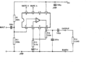

FIGURE 9-6 Audio amplifier with muting characteristics (GEC Plessey, Professional Products 1991 p. 1–150)
9.2.1 Muting Function
Muting signals are applied at both mute A (pin 7) and mute B (pin 8) terminals. For normal operation, the mute A pin is left open-circuit or is connected to a voltage within 0.65 V of VCC (through a 100-k resistor). When the voltage on pin 7 is reduced to within 1 V of ground (through a 100-k resistor), the IC is muted.
9.2.2 Voltage Gain and Frequency Response
Because the IC is essentially an op-amp, the voltage gain and frequency response can be controlled by external components in the usual manner. Figure 9-7 shows typical gain versus frequency characteristics.

Voltage gain is set by the ratio (R3 + R4)/R3 and should be between 3 and 30 for best results (good stability).
The low-frequency rolloff point is set by the value of the capacitor in series with resistor R3.
The high-frequency limit is set by the IC characteristics (Fig. 9-7), but can be reduced by connecting a capacitor across R4.
9.3 Low-Noise High-Frequency Amplifier
Figures 9-8 and 9-9 show the circuit schematic and PC-board layout, respectively, for a low-noise amplifier capable of operating beyond 300 MHz. This IC (the GEC Plessey SL560) contains three high-performance transistors connected in a unique circuit. As shown in Fig. 9-8, there are multiple-input options, as well as gain-set and current-set provisions. This arrangement permits maximum flexibility with a minimum of external components.
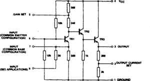

FIGURE 9-9 PC-board layout for low-noise amplifier (GEC Plessey, Professional Products, 1991, p. 1–63)
9.3.1 Circuit Description
The input transistor TR1 is normally operated in the common-base mode. This provides a well-defined low-input impedance. Transistor TR1 provides the full voltage gain. The output at the collector of TR1 is buffered by the two emitter-followers TR2 and TR3. Note that there are two common-base inputs: a direct input at pin 7 and a 50-ohm input at pin 8.
To get maximum bandwidth, the capacitance at the collector of TR1 must be kept at a minimum. For this reason, the collector of TR1 is not brought out of the package (to avoid bonding-pad and can capacitances). However, the collector load of TR1 is split, with the tap brought out to pin 5. An external rolloff capacitor can be connected at pin 5 to alter the gain-frequency and bandwidth characteristics, as described in Chapter 3.
The input transistor TR1 can also be operated in the common-emitter mode by decoupling pin 7 and using pin 6 as the input. In this configuration, the noise figure is about 2 dB when the source resistance is 200 ohms.
9.3.2 PC-Board Layout Considerations
No matter what operating mode is selected, care must be taken to avoid high-frequency instability. Figure 9-9 shows a recommended PC-board layout for both common-base and common-emitter modes. As always, keep capacitor leads as short as possible and use small capacitors where practical. A ground plane is strongly recommended.
9.3.3 Common-Base Line Driver
Figure 9-10 shows the IC connected as a common-base 200-MHz line driver, with 50-ohm input and output. Figure 9-10 also shows the input standing wave ratio plot versus frequency for the common-base circuit. Note that only three external components are required (three 10-nF capacitors).
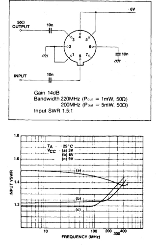
To get the 50-ohm input, pin 8 is connected to the input through a 10 nF coupling capacitor. This applies the input signal to the emitter of TR1 through an internal 30-ohm resistor. To get the 50-ohm output, pin 2 is connected to pin 1 and ground. This shorts the internal 2-k resistor at the emitter of TR3. The output is taken from the junction of the internal 200-ohm resistor and the emitter of TR3.
Because no rolloff capacitor is required, pin 5 is connected to +6 V, along with the normal power input at pin 4. This shorts the internal 560-ohm resistor at the collector of TR1 and sets the voltage gain at about 14 dB (for the common-base mode). When pin 5 is left open (no connection) the gain increases. This is not recommended for common-base operation.
The common-base configuration is achieved by connecting pin 6 to ground through a 10-nF capacitor (instead of directly to ground). Pin 7 is left open in this configuration, but is used when inputs other than 50 ohms are required. Pin 1 is connected to ground, and pin 4 is connected to power or VCC (which can be as high as + 15 V).
9.3.4 Common-Emitter Low-Noise Preamplifier
Figure 9-11 shows the IC connected as a common-emitter low-noise preamplifier. Figure 9-11 also shows the gain-frequency response for this configuration. Again, three 10-nF coupling-decoupling capacitors are required, plus a 10-k resistor at the input (thus increasing the input impedance).

FIGURE 9-11 Common-emitter low-noise preamplifier (GEC Plessey, Professional Products, 1991, p. 1–65)
In this configuration, pin 2 is not connected, allowing the 2.2-k resistance at the emitter of TR3 to appear at the output (pin 3). Pin 5 is also not connected, placing both the 560-ohm and 240-ohm resistors in the collector of TR1. This raises the amplifier gain to the 32- to 35-dB range (depending on the supply voltage at pin 4).
The common-emitter configuration is achieved by connecting pin 7 to ground through a 10-nF capacitor and by leaving pin 8 disconnected. (Note that Fig. 9 referred to in Fig. 9-11 is the gain-frequency graph of Fig. 9-11.)
9.3.5 Common-Emitter Wideband Amplifier
Figure 9-12 shows the IC connected as a common-emitter wideband amplifier, with a − 1-dB rolloff at 6 MHz and 300 MHz. Figure 9-12 also shows the gain-frequency response for this configuration. Note that additional external components are required to get the high- and low-end rolloffs shown in the response curve.

In this configuration, pin 2 is not connected, allowing the 2.2-k resistance at the TR3 emitter to appear at the output (pin 3). Pin 5 is connected to VCC, along with the power input at pin 4. Again, this shorts the internal 560-ohm resistor at the TR1 connector and sets voltage gain at about 14 dB (depending on the value of VCC).
The common-emitter configuration is achieved by connecting pin 7 to ground through an RC filter network and by leaving pin 8 disconnected. This RC filter combines with the RC feedback network between input pin 6 and output pin 3 to produce the wideband frequency response (with 1-dB rolloff at both 6 MHz and 300 MHz).
9.4 Low-Noise Wideband Amplifier with External Gain Control
Figures 9-13 and 9-14 show the circuit schematic and test circuit, respectively, for a low-noise, wideband amplifier with external gain control. This IC (the GEC Plessey SL550) is a general-purpose wideband linear amplifier with remote gain control.

FIGURE 9-13 Low-noise wideband amplifier with gain control (GEC Plessey, Professional Products, 1991, p. 1–56)

At a frequency of 60 MHz, the IC noise figure is a typical 1.8 dB from a 200-ohm source. The gain-control provision can be used for swept-gain applications, and makes the IC suitable for use in linear IF strips or as a low-noise preamp for log IF strips.
The external gain control is performed in the feedback loop of the main amplifier (at pins 2 and 3). The main amplifier is buffered at both the input and output. As a result, the noise figure and output voltage swing are only slightly degraded when the gain is reduced. The gain control has a specified accuracy of ± 1 dB. The input transistor can be connected in the common-emitter or common-base modes (at pins 11 and 12). The quiescent current of the output emitter-follower can be increased to permit operation with low-impedances loads.
9.4.1 Input Impedance
The input capacitance, which is typically 12 pF at 60 MHz, is independent of frequency. The input resistance, which is about 1.5 k at 10 MHz, decreases with frequency and is typically 500 ohms at 60 MHz.
9.4.2 Gain-Control Input
Gain control is normally provided by applying a current into pin 2. There is a forward-biased diode between pin 2 and ground. As a result, the voltage at pin 2 varies between 600 mV (with a current of 1 μA) to 800 mV (with a current of 2 mA). The amplifier gain is varied by applying a voltage in this range to pin 3. Figure 9-15 shows the relationship between control current and amplifier gain. Note that the gain can be fixed when pins 2 and 3 are connected to the power (VCC) through a fixed resistor.

To avoid problems associated with control-voltage sensitivity and with operation over a wide temperature range, the diode at pin 2 should be used to convert a control current to a voltage that is applied to pin 3. This is done by connecting both pins 2 and 3 to the AGC voltage source as shown.
9.4.3 Minimum Supply Current
If the full output swing is not required, or if high impedance loads are being driven, the current consumption can be reduced by omitting R1 shown in Fig. 9-14. The function of R1 is to increase the quiescent current of the output emitter-follower. A typical value of R1 is 750 ohms. With this value, the output voltage swing is about 0.3 Vrms and supply current is a typical 15 mA. When R1 is omitted, the output voltage swing drops to about 0.15 Vrms and supply current drops to a typical 11 mA.
9.4.4 High-Impedance Current Output
A high-impedance current output can be obtained by taking the output from pin 6 and leaving pin 7 open circuit (disconnected). Under these conditions, the maximum output current is 2 mA peak and the output impedance is 350 ohms.
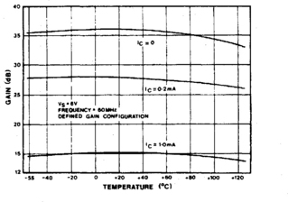
9.4.5 Decreasing Gain Variation with Temperature
The gain variation with temperature can be reduced (at the expense of noise figure) by including the internal 30-ohm resistor in the emitter of the input transistor. This is done by decoupling pin 13 (with a 10-nF capacitor to ground) and leaving pin 12 open circuit. The IC then operates in the common-emitter mode with the input at pin 11. The IC can also be operated in the common-emitter mode by decoupling pin 12 and leaving pin 13 open circuit, as shown in Fig. 9-14. This improves the noise figure, but does degrade the gain-temperature relationship, as shown in Figs. 9-16 and 9-17.

9.4.6 Low-Input Impedance
A low-input impedance (about 25 ohms) can be obtained by connecting the input transistor for common-base operation. This is done by decoupling pin 11 and applying the input to pin 12 (with pin 13 open circuit).
9.4.7 High-Frequency Stability
As always, care must be taken to keep all capacitor leads short and a ground plane should be used. The main concern is stray inductance or capacitance between the input and output. The 30-ohm resistor (at pin 14) shown in Fig. 9-14 eliminates high-frequency instability because of strays (which are common in a plug-in test system). If the IC is soldered directly into a PC board, the 30-ohm resistor can be reduced in value or possibly omitted completely.
9.4.8 Two-Stage Wideband Amplifier
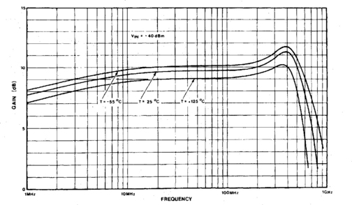
Figure 9-18 shows two SL550s connected in series to form a wideband amplifier. Note that the input stage is connected for common-emitter operation (input applied at pin 11), with the output stage connected in the common-base mode (input applied at pin 12). In both cases, pin 13 is left open circuit. The bandwidth is approximately 5 to 130 MHz, with a noise figure slightly 2 dB.
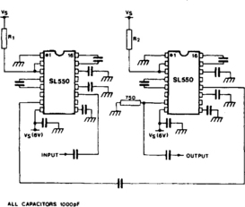
With a 750-ohm resistor at pin 7, the output voltage swing is about 0.3 Vrms. Supply current for the output IC is about 15 mA and about 11 mA for the input IC (no resistor at pin 7). Stable gains up to about 65 dB can be obtained by proper selection of R1 and R2. Use Fig. 9-15 to find the control current required to produce a given gain for each stage. For example, a current of 1 mA should produce a gain of about 22 dB in each stage. The values for R1 and R2 need not be the same. However, in no case should the current at pin 2 exceed 10 mA or the current at pin 3 exceed 1 mA.
9.5 True-Log IF Amplifier
Figures 9-19 and 9-20 show the circuit schematic and typical test/applications, respectively, for a true-log IF amplifier (the GEC Plessey SL531). Figure 9-21 shows the electrical characteristics. The IC is designed for use in logarithmic IF amplifiers of the true-log type. The input and log output of a true-log amplifier are at the same frequency (there is no detection of the signal). In successive-detection log amplifiers (see Section 9.6), the log output is detected.


As shown in Fig. 9-21, the small-signal gain is a typical 10 dB and bandwidth is over 500 MHz. At high signal levels, the gain of a single stage drops to unity. A cascade of individual stages gives a close approximation to log characteristics at center frequencies between 10 and 200 MHz.
An important feature of the IC (from a simplified design standpoint) is that the phase shift is nearly constant with signal level. This means that any phase information on the input signal is preserved through the IF strip.
9.5.1 Circuit Description
For small-signal inputs (where the input signal is less than 0.2 V), the IC has a nominal gain of 10 dB. When the input is large signal (input signals between 0.2 and about 0.8 V), the gain drops to unity. This is done by operating a limiting amplifier and a unity-gain amplifier in parallel. Transistors TR1 and TR4 form the limiting amplifier, with current being supplied by TR5. Transistors TR2 and TR3 form the unity-gain amplifier. The gain is set by the 130-ohm emitter resistors. The outputs of both stages are summed in the 300-ohm resistor. Transistor TR7 acts as an emitter-follower output buffer. Note that the constant phase-shift and amplitude characteristics are provided by the unity-gain amplifier (TR2/TR3). Current for this amplifier is provided by transistor TR6.
9.5.2 Supply Voltage Options
An on-chip resistor (at pin 8) can be used to drop the supply voltage, instead of the external 180-ohm resistor shown in Fig. 9-20 (thus minimizing parts count). However, the extra dissipation of the internal resistor (166 ohms) reduces the maximum operating temperature to 100°C from the 125°C maximum with the external resistor.
It is also possible to use a 6-V supply connected directly to pins 1 and 2 instead of the nominal 9-V supply with an external resistor. However, the omission of a dropping resistor in the supply might cause feedback on the line. RF chokes (between stages) can be used in the supply line to eliminate feedback problems.
9.5.3 Layout Precautions
The internal 200-pF decoupling capacitors (pins 1 and 5) help prevent high-frequency instability. However, normal high-frequency layout precautions still apply. (Coupling capacitors should be physically small and be connected with short leads.) It is most important that the ground connections be made with short leads to a continuous ground plane.
9.5.4 Low-Frequency Response
Figure 9-22 shows the small-signal frequency response when the IC is connected as shown in Fig. 9-20. The low-frequency response is determined by the on-chip decoupling capacitors, but can be extended with external decoupling capacitors connected at pins 1 and 5 (to ground).
9.5.5 Six-Stage Log IF Strip
Figure 9-23 shows six SL531s connected as a 6-stage true-log IF strip. An SL560 (see Section 9.3) is used as a unity-gain buffer. The output of the log strip is attenuated (ahead of the SL560) to provide a nominal 0-dBm output into 50 ohms.
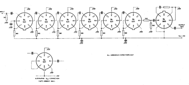
The supply voltage is fed to each stage through an external 180-ohm resistor. This allows operation at temperatures up to 125°C ambient. If the ambient temperature can be limited to + 100°C, then the internal resistor can be used to reduce the external parts count. Use the alternate VCC connection shown, where pin 8 is connected directly to +9 V and pin 1 is connected to pin 2.
Interstage coupling is simple and requires a single capacitor between stages. However, it is important to provide extra decoupling on pin 1 of the first stage to prevent possible feedback on the supply line. No connection is necessary to pin 5 unless operation below 10 MHz is required.
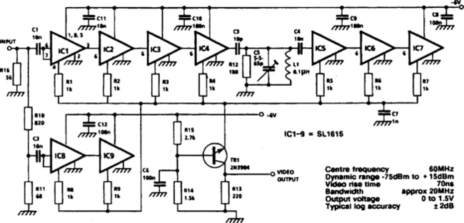
9.6 Successive-Detection Log Amplifier
Figures 9-24 and 9-25 show the circuit schematic and typical applications diagram, respectively, for a wideband successive-detection log amplifier (the GEC Plessey SL1615). Figure 9-26 shows the electrical characteristics. The IC is designed for use in logarithmic IF amplifiers of the successive-detection type (where the output is detected). There is also a separate RF output. The IC is best suited for IF strips operating in the 10- to 60-MHz center-frequency range and provides amplification, limiting, and detection of the input signal. When more than one IC is used, no coupling capacitor is required between stages.
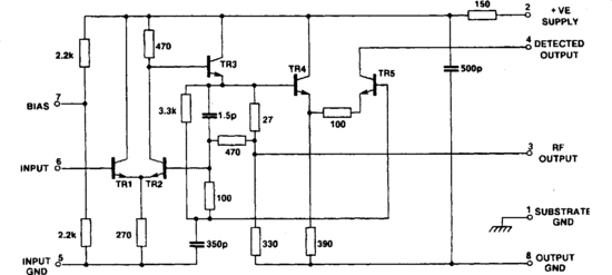


FIGURE 9-26 Successive-detection log amplifier characteristics (GEC Plessey, Professional Products, 1991, p. 1–29)
9.6.1 Design Considerations
Although the interconnections are simple, as shown in Fig. 9-25, there are certain precautions to be observed. The following is a summary of these precautions.
The supply line is provided with an internal 500-pF decoupling capacitor (at pin 2, through a 150-ohm resistor). This capacitor is of the junction type and has a low breakdown voltage. If the supply voltage exceeds 7.5 V, breakdown can occur and the positive supply current will increase rapidly.
The supply line also requires an external decoupling capacitor as shown. The value of the capacitor depends on the number of stages involved. If there are six or more stages, the minimum capacitance is 30 nF. For IF strips with less than six stages, the minimum values for the supply-line decoupling capacitors are 5 stages = 10 nF, 4 stages = 3 nF, and 3 stages = 1 nF.
Note that the ICs have two signal ground leads (input at pin 5 and output at pin 8). There is also a substrate ground at pin 1. This is to avoid the introduction of common-ground lead inductance between the input and output circuits. (As usual, use a ground plane to avoid any stray inductance between input and output.)
When there are seven stages involved, the seventh stage of an untuned cascade produces virtually full output on noise. This noise can be reduced by inserting a single tuned circuit in the chain. Because there is a large mismatch between stages and because the log output must be preserved, a simple parallel or series circuit cannot be used. Figure 9-27 shows a suitable network. The value of C5 is adjusted so that the C5 admittance equals the loss conductance across the tuned circuit. (In effect, C5 is adjusted until the output is at the correct log value for a given input.)
9.7 Single-Chip Successive-Detection Log/Limiting Amplifier
Figures 9-28 and 9-29 show the circuit schematic and typical test/applications diagram, respectively, for multistage log/limiting amplifier contained within a single IC. Figure 9-30 shows the electrical characteristics. The IC (the GEC Plessey SL3522) can operate over an input frequency range of 100 to 600 MHz and produce a log/linear output for signals between −68 to +7 dBm, with a log accuracy of ± 1 dB.

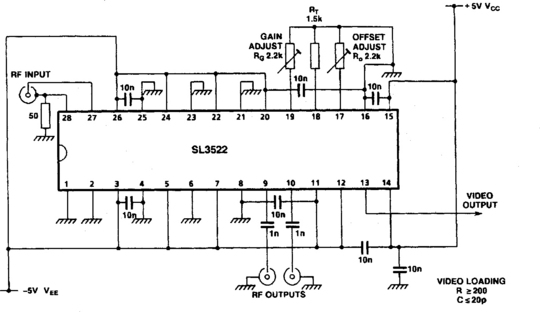
FIGURE 9-29 Single-chip log/limiting amplifier test/applications (GEC Plessey, Professional Products, 1991, p. 1–5)
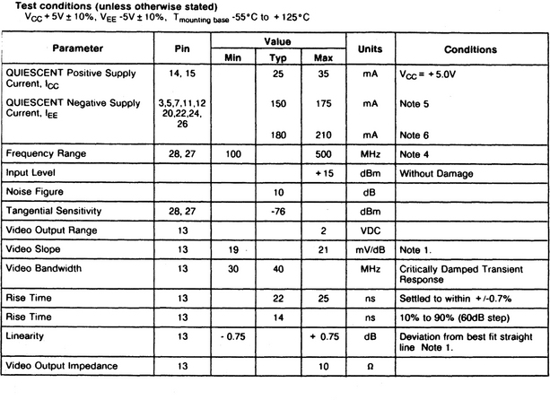

FIGURE 9-30 Single-chip log/limiting amplifier characteristics (GEC Plessey, Professional Products, 1991, p. 1–4)
As shown in Fig. 9-28, the IC contains six gain stages, seven detector stages, a limiting RF-output buffer, and a video-output amplifier. The power-supply connections to each section are isolated from each other to increase stability. Each of the gain stages and the detector stages has about 12 dB of gain. On-chip RF decoupling (not shown) also aids stability.
The limiting RF-output buffer provides a balanced limited-output level of 0 dBm on each RF-output line (pins 9 and 10) for signal levels in excess of −65 dBm (with the input applied at pins 27 and 28). The RF-output buffer can be isolated from the other parts of the amplifier circuit by disconnecting the RF-output buffer ground (pin 8). This feature aids stability in applications that do not require a limited RF output.
The video amplifier provides a positive-going output signal proportional to the log of the amplitude of an RF input applied at pins 27 and 28, as shown in Fig. 9-29. The gain and offset of the video amplifier can be adjusted by means of three resistors, RG, RT, and RO, which are connected to the gain-adjust terminal (pin 19), trim reference terminal (pin 18), and offset-adjust terminal (pin 17), respectively.
With RT set at 1.5 k, RG can be set to any value between 1 k and 2.2 k to get a ±20% log-slope range. Resistor RO can be set to any value between 1 and 2.2 k to get an offset in the range between 0.5 and + 1 V.
The RF-input terminals (pins 27 and 28) have a 50-ohm on-chip terminating resistor connected between them. In turn, pins 27/28 are capacitively coupled to the input gain stage. The RF input can be driven balanced or single-ended.
The IC consumes about 1.1 W of power when all parts of the circuit are powered from a ±5-V supply. Because the circuit uses a class A differential configuration, the power consumption of the RF gain stages, detectors, and RF-output buffers are independent of input signal level. However, the video output (pin 13) is single-ended and the power consumption of the video amplifier varies with RF-input signal level (pins 27/28).
If the IC is to be operated with the RF-output buffer disabled (RF-output buffer ground pin 8 left floating), the power consumption drops to about 0.95 W (when all other parts of the circuit are powered from a ±5-V supply).
9.7.1 RF-Output Buffer
The IC produces an output with 70 dB of broadband RF gain and 3-dB bandwidth at 450 MHz. When the RF-output buffer is powered up, this output appears at the RF-output terminals (pins 9 and 10). Operating the IC with the RF-output buffer powered down removes the RF output, but leaves a log output at pin 13.
Note that the RF-output ground terminal (pin 8) is the positive supply to the RF-output buffer. If pin 8 is left open circuit, the RF-output buffer powers down and saves 30 mA of power consumption from the VEE (–5 V) supply.
The RF-output VEE terminal (pin 11) must always be connected to the VEE supply, even if the RF-output buffer is powered down (by leaving pin 8 open). Note that with pin 8 connected to ground and pin 11 connected to VEE, as shown in Fig. 9-29, the RF-output buffer is operating and there are RF outputs at pins 9 and 10. If the RF-output buffer is used instead of (or in addition to) the video output, extra care must be taken in layout. For example, if the RF output should leak back to the RF input, the IC might become unstable. This is not likely to happen when only the video output at pin 13 is used.
9.7.2 Layout Suggestions
The following manufacturer’s suggestions should be followed when connecting the device in any application (RF output, video output, or both).
1. The IC should be mounted on a ground plane and all supply decoupling capacitors should be surface-mount, RF-quality, low-loss chip capacitors. The capacitor leads should be kept as short as possible.
2. The RF VEE terminals (pins 3, 5, 7, 20, 22, 24, and 26) should connect to a low-impedance copper plane. A two-layer PC board can provide such a connection.
3. The load current at the video-output terminal (pin 13) should be returned to the video-output VCC terminal (pin 14) through a 10-nF capacitor connected to the return line of the video load. This avoids any common-impedance path.
The video-output VEE terminal (pin 12) should be decoupled directly to the video-output VCC terminal (pin 14) with a 10-nF capacitor.
The unscreened lead length at the RF input should be kept to a bare minimum. If being driven single-ended, the RF-input return line should be isolated from (but kept in very close proximity to) the ground plane and connected to the ground plane through a 50-ohm chip (or bead) resistor at pin 28, as shown in Fig. 9-29. This resistor is not required when the RF input is differential.
If the IC is operated with the RF-output buffer powered up, care must be taken to present both the RF-output terminals (pins 9 and 10) with matched loads. Ideally, each pin should be loaded with a 50-ohm terminated transmission line. The IC stability is very sensitive to imbalance at the output. Driving highly reactive SWR loads is not recommended for stability reasons.
Although the RF-output terminals (pins 9 and 10) are shown with 1-nF blocking capacitors in Fig. 9-29, the outputs can be operated with a DC load to ground. However, a DC offset of about −400 mV will exist on each RF-output pin. In addition, when the outputs are operated with a DC load to ground, it is not possible to power-down the RF-output buffer.
The RF-input terminals (pins 27 and 28) are isolated from the input amplifier by two 20-pF on-chip capacitors. There is a 50-ohm on-chip termination resistor connected across pins 27 and 28. This makes it possible to operate the RF input single-ended, or differential, to suit a variety of applications.
9.7.3 Gain and Offset Trimming
Gain and offset trimming are unilaterally independent. That is, adjustment of gain has an effect on the offset, but adjustment of offset does not affect the gain.
The gain and offset control is achieved by adjusting RG and RO, respectively. The control depends on the difference between RG and RT or between RO and RT. (RT is the trim-reference resistor.)
Differing temperature coefficients in all three resistors will lead to variations in gain and offset over the temperature range. As a result, it is recommended that resistors of identical type be used for gain-offset trimming.
9.7.4 Video Performance
To get the specified video-transient performance (Fig. 9-30), make certain that the trim-reference resistor (connected at pin 18) has a parasitic capacitance less than 5 pF. This resistor should have a nominal value of 1.5 k. In addition, the video load should be at least 200 ohms resistive, with not more than 20 pF of shunt capacitance, as shown in Fig. 9-29.