Chapter 11
In this chapter a complete preamplifier is described, to bring to life the various circuit blocks described in other chapters. The design is basically that of the ‘Precision Preamplifier 96’ published in Electronics World in July–September 1996 [1]. The description here is fairly concise because most of the circuit blocks are fully described in the relevant chapters of this book.
Architecture and Philosophy
The preamplifier architecture is as established in Chapter 6. The moving-magnet (MM) phono amplifier gain is +29 dB, raising an input of 5 mVrms (all gains and levels are at 1 kHz) to a line-out level of 150 mVrms nominal, matching equipment levels that appear to have reached some sort of consensus on this value.
The separate moving-coil (MC) stage will accept inputs of 0.1 or 0.5 mV and gives an output of 5 mV that is suitable for the MM input stage. The MC stage provides flat gain, while the MM stage performs the RIAA equalization for both modes. The MM stage is followed by a third-order subsonic filter, which also implements the IEC Amendment. There are an odd number of half-5532s, so the single 5534 is placed in the MM stage, where its somewhat lower noise is put to best use. The MC input amplifier is fully described in Chapter 8, and the MM input amplifier and subsonic filter is fully described in Chapter 7. Full schematics of these circuit blocks are given there.
The phono amplifier stages feed one input of the input selector switch bank, which is followed by the unbuffered recording output, the recording input, and the monitoring switch that selects between them (see Figure 11.1). The principle of low-crosstalk input select switching is covered in Chapter 16.

Figure 11.1: Block diagram of the complete preamplifier
The next stage is an input buffer to give low-impedance drive to the tone-control stage. It has a gain variable over a small range by the balance control; its gain is +1.1 dB with balance central. The tone-control stage that follows has fully variable turnover frequencies and a non-interrupting tone-cancel facility. The tone control phase-inverts, but this is reversed by the active gain control system (AGS) after it. The maximum gain of the AGS is +17 dB, giving a maximum output of 1 Vrms for a line input of 150 mVrms.
The philosophy of this design is to achieve low noise by minimizing circuit impedances so the contribution of Johnson noise is reduced, and the conditions are set for best bipolar op-amp noise performance. The balance control, tone control, and volume control are all active gain configurations to eliminate even small compromises resulting from attenuation-then-amplification (increased noise) or amplification-then-attenuation (reduced headroom). Absolute phase is preserved for all input and outputs.
Another design aim was to make as many components in the design as possible the same value, to simplify procurement. All the pots are 10 kΩ linear; most sizeable non-electrolytics are 470 nF, most small electrolytics are 10 μF 50 V, and all large ones are 220 μF 35 V. This philosophy has to be abandoned in areas where critical parameters are set, such as in the RIAA network and tone-control stage.
The Line Inputs
The input is selected by a push-button switch bank rather than a rotary control, as this allows a four-pole configuration to be used that much improves the rejection of unselected inputs. This is fully described in Chapter 16 on signal switching.
The CD input stands out from other line sources in that its nominal level is usually high at 2 Vrms. This is possible because digital sources have rigidly defined maximum output levels, so they can be high to improve noise performance, since there is no danger of the analog output section clipping. However, this means a direct line input cannot be used without the trouble of resetting volume and recording-level controls when CD is selected. To minimize this problem a 16 dB passive attenuator, as shown in Figure 16.1b, is placed in the CD input path. The assumption is that a CD output has a low impedance, and will have no problem driving a 10 kΩ input impedance. The divider resistance values can therefore be made low to minimize the noise degradation. The output impedance of the attenuator is 1.4 kΩ, which generates −120.9 dBu of Johnson noise as opposed to −135.2 dBu from a direct 50 Ω source. This is still much less than the preamp internal noise so the noise performance is not worsened. Inter-source crosstalk is improved simply by back-grounding the CD attenuator output when not in use, so only a two-pole switch is required for good isolation of this source.
The High-Impedance Input Buffer
It can be argued that the input impedance of a preamplifier should be high to allow for interfacing to valve equipment whose output may be taken from a valve anode, where even light loading compromises distortion and available output swing. A plausible minimum input impedance for this is 100 kΩ; many preamplifier designs fall well short of this.
This stage therefore has to provide both a high input impedance and a variable gain for the balance control. This is a vernier balance control that alters relative channel gain by only +4.5, −1.1 dB, a difference of 6 dB; this is sufficient to move the stereo image completely from one side to the other. Since the minimum gain of this non-inverting stage is unity, the nominal gain with balance control central is +1.1 dB, and the maximum gain of the active gain stage (AGS) is chosen to allow for this. The active nature of the balance control means that the signal never receives unwanted attenuation that must be undone later with noisy amplification.
The input buffer is shown in Figure 11.2. A high input impedance is obtained simply by using a 470 kΩ biasing resistor R2, accepting that the bias current through this will give a negative output offset of 95 mV typical; this is not big enough to significantly reduce headroom. The gain law is modified by R3 to give as little gain as possible in the central control position. Maximum gain is set by R4, and DC gain held to unity by C4; R1 and C2 make up an EMC filter. The noise output of the buffer/balance stage is of the same order as the test-gear and cannot be measured directly – a subtraction method gives a noise output of about −116 dBu with balance central.

Figure 11.2: The high-input-impedance buffer, with variable gain for balance control
An important point is that the significant bias current of the op-amp inverting input is not allowed to flow through the balance pot; this would make it noisy. The bias current has a separate DC path through R3, while the AC feedback goes through C3.
The Tone-Control Stage
The tone-control stage is described here rather than in Chapter 10, because it is specialized in that it aims at very good noise performance. The design is not a conventional Baxandall tone control. It has break frequencies variable over a 10:1 range, which makes the facility much more useful for correcting speaker deficiencies. This extra flexibility may fly right in the face of subjectivist thinking, but I can live with that. Variable boost/cut and frequency enables any error at the top or bottom end to be corrected to at least a first approximation. It makes a major difference.
Certain features of the tone control may make it more acceptable to those prey to doubts about its sonic correctness. The tone-control range is ±10 dB, rather than the ±15 dB standard in mixing consoles. The response is built entirely from simple 6 dB/octave circuitry, with inherently gentle slopes. The stage is naturally minimum phase, and so the amplitude curves uniquely define the phase response. The maximum phase-shift does not exceed 40° at full boost. This is a return-to-flat (RTF) tone control, meaning that the curves do not plateau or shelve at their boosted or cut level, but smoothly return to unity gain outside the audio band. Boosting 10 kHz is one thing, but boosting 200 kHz is quite another, and could lead to some interesting stability or EMC problems. The RTF time-constants are fixed so the boost/cut range is necessarily less at the frequency extremes, where the RTF effect starts to overlap the variable boost/cut frequencies.
The basic principle is shown in Figure 11.3. The overall stage gives a unity-gain inversion except when the selective responses of the side-chain paths allow signal through. In the treble and bass frequency ranges where the side-chains pass signal, the boost/cut pots VR2, VR4 can give either gain or attenuation. When a wiper is central, there is a null at the middle of the boost/cut pot, no signal through that side-chain, and the gain is unity.
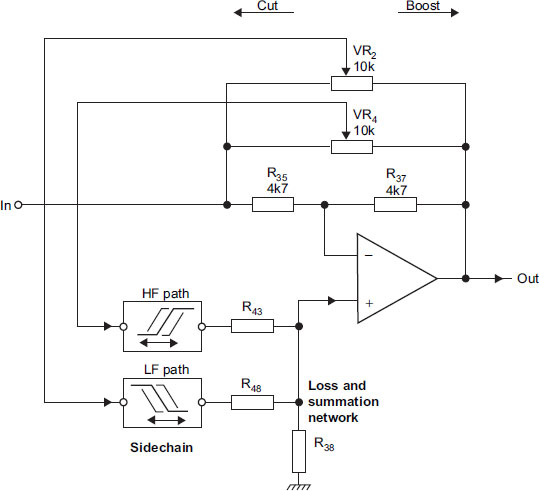
Figure 11.3: The principle of the tone-control stage. The response only deviates from unity gain at frequencies passed by the HF or LF paths
If the pot is set so the side-chain is fed from the input then there is a partial cancellation of the forward signal; if the side-chain is fed from the output then there is a partial cancellation of the negative feedback, or to put it another way, positive feedback is introduced to counteract part of the NFB through R37. This apparently ramshackle process actually gives boost/cut curves of perfect symmetry, though this is purely cosmetic, because you can’t use both sides of the curve at once, so it hardly matters if they are exact mirror images.
The tone-control stage acts in separate bands for bass and treble, so there are two parallel selective paths in the side-chain. These are simple RC time-constants, the bass path being a variable-frequency first-order low-pass filter, and the associated bass control only acting on the frequencies this lets through. Similarly the treble path is a variable-frequency high-pass filter. The filtered signals are summed and returned to the main path via the non-inverting input, and some attenuation must be introduced to limit cut and boost. Assuming a unity-gain side-chain, the necessary loss is 9 dB if cut and boost are to be limited to ±10 dB. This is implemented by R43, R48, and R38 in Figures 11.4–11.6. The side-chain has unity gain, and so has no problems with clipping before the main path does, so it is very desirable to put the 9 dB loss after the side-chain, where it attenuates side-chain noise. The loss attenuator is made up of the lowest value resistors that can be driven without distortion, to minimize both the Johnson noise thereof and the noise generated by op-amp IC7b.
The tone-cancel switch disconnects the entire side-chain (i.e. five out of six op-amps) from any contribution to the main path, and usefully reduces the stage output noise by about 4 dB, depending on the HF frequency setting. It leaves only IC7b in circuit, which must be retained anyway to undo the gain-control phase inversion. Unlike configurations where the entire stage is bypassed, the signal does not briefly disappear as the cancel switch moves between two contacts. This minimizes transients due to suddenly chopping the waveform and makes valid tone in/out comparisons much easier.
It is very convenient if all the pots in a design are identical, and I am quite proud of having achieved it here. I have used linear 10 kΩ controls throughout to avoid log-pot tolerances. This has required some thoughtful circuit design to give all the controls the logarithmic action that fits our perceptual processes. It is, however, desirable for the balance and the tone-control cut/ boost pots to have central detents, which somewhat goes against the ‘all pots identical’ philosophy.
The basics of the HF path are shown in Figure 11.4. C32 and R41 are the high-pass time-constant, driven at low impedance by unity-gain buffer IC6b. This buffer prevents the high-pass frequency from changing with the boost/cut setting. The effective value of R41 is altered over a 10:1 range by varying the amount of bootstrapping it receives from IC7a, the potential divider effect and the rise in source resistance of VR5 in the center combining to give a reasonable approximation to a logarithmic frequency/rotation law, as shown in Figure 11.8 below. R42 is the frequency end-stop resistor that limits the maximum effective value of R41. C29 is the HF RTF capacitor – at frequencies above the audio band it shunts all the side-chain signal to ground, so the treble control no longer has any further effect.

Figure 11.4: HF path of the tone control
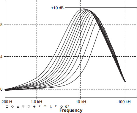
Figure 11.8: AHF boost curves of the tone control
The treble side-chain degrades the noise performance of the tone-control stage by 2−3 dB when connected. As would be expected, the noise contribution is greatest when the HF frequency is set to minimum, and a wider bandwidth from the side-chain is contributing to the main path.
The simplified LF path is shown in Figure 11.5. IC6a buffers the cut/boost control VR2 to prevent boost/frequency interaction. The low-pass time-constant capacitor is C37, and the associated time-constant resistance is a combination of VR3 and R45, R46. The RTF time-constant for the bass path is set by C38 and R47, which block very low frequencies and so limit the lower extent of bass control action. The bass frequency law is made approximately logarithmic by IC8b; for minimum frequency VR3 is set fully anticlockwise, so the input of buffer IC8b is the same as at the C37 end of R46, which is thus bootstrapped and has no effect. When VR3 is fully clockwise, R45, R46 are effectively in parallel with VR3 and the turnover frequency is at a maximum. The presence of R45 gives an approximately logarithmic law (see Figure 11.7). Compared with the HF path, an extra op-amp is required. However, despite this, the bass side-chain contributes very little extra noise to the tone stage. This is because most of its output is rolled off by the low-pass action of C37 at high frequencies, almost eliminating its noise contribution.

Figure 11.5 : LF path of the tone control

Figure 11.7: LF boost curves of the tone control
Once the active elements (here 5532s) have been chosen, and the architecture made sensible in terms of avoiding attenuation-then-amplification, keeping noise gain to a minimum, and so on, the remaining way of improving noise performance is by impedance reduction of the circuitry. The resistances are lowered in value, with capacitances scaled up to suit, by a factor limited only by the op-amp drive capability. This is another good reason to use the 5534/2. Two examples of this process as applied to the tone stage are given here. In each case the noise improvement is for the stage in isolation, set flat with HF frequency at minimum:
In this kind of stage R36, R37 are conventionally 22 kΩ. Using 4k7 instead dropped the noise output by 1.3 dB.
The summation/loss network began life with R43, R48 at 4k7, and R38 at 5k6. Reducing this by a factor of 10, to 470 and 560 Ω respectively, reduced output noise by 0.6 dB.
Neither of these improvements is startling in itself, but both cost nothing, and they all add up. The noise output of the tone stage, plus the line/balance buffer before it, with balance control central and tone cancel pressed, is −107.2 dBu (22 kHz bandwidth). With tone controls active but set flat, noise output at minimum HF frequency is −104.7 dBu, and at maximum HF frequency is −106.7 dBu.
The final tone stage and the AGS are shown in Figure 11.6. The tone section may look rather a mess of pottage, and appear to have more buffers than Clapham Junction, but this modest degree of complexity is required if control interaction is to be wholly eliminated.

Figure 11.6: Full schematic of the tone control and active gain stage
The practical tone circuitry contains more capacitors than the simplified circuits in Figures 11.4 and 11.5, and this reflects a disadvantage of low-noise bipolar input op-amps. The bias currents are non-negligible and must not be allowed to flow through potentiometers if crackling noises are to be avoided when they are moved. These bias currents also tend to cause significant output offset voltages; the source resistances for the two op-amp inputs are not normally the same and so there is no offset cancellation. For this reason all the variable-gain circuit sections have their gain reduced to unity at DC by blocking capacitors. C31 and C35 keep bias currents out of VR2, VR4, necessitating bias resistors R40, R44.
The treble frequency law is corrected by bootstrapping through C33, which keeps the bias current of IC7a out of VR5. Similarly C34 prevents any offset on IC7a output reaching VR5. In the bass path C36 keeps IC8b bias out of VR3, while RTF components C38, C39 and R47 inherently provide DC blocking. The final offsets at the side-chain output are blocked by C40, while the bias voltage on non-inverting input IC7b is blocked by C30. This is essential to prevent the tone-cancel switch clicking. This switch may still appear to click if it switches in or out a large amount of response modification of a non-zero signal, because the abrupt gain change generates a step in the waveform that is heard as a click. This is unavoidable with hard audio switching.
The maximal cut and boost curves over the frequency ranges are shown in Figures 11.7 and 11.8. Figure 11.9 collates the measured extremes of cut and boost at the frequency extremes.

Figure 11.9: Maximum cut and boost curves of the tone control at the frequency setting extremes
The Active Gain Stage
The active gain stage (AGS) used here is the Baxandall configuration [2], which I have used previously in another preamplifier design [3]. The maximum gain is set to +17 dB by the ratio of R52 to R53. This active volume-control stage gives the usual advantages of lower noise at gain settings below maximum, and in the special case of the Baxandall configuration, excellent channel balance that depends solely on the mechanical alignment of the dual linear pot – all mismatches of its electrical characteristics are canceled out, and there are no quasi-log dual slopes to induce anxiety. The noise performance has been improved by an impedance reduction on the gain-definition network R52, R53. The limit on this is the ability of buffer IC5a to drive R52, which has a virtual earth at its other end.
There are the usual complications to deal with the DC: C41 keeps IC7b output offset out of volume control VR6, while C42 blocks IC5a bias current from VR6 wiper. C44 gives final output DC blocking. Details of the volume-control law and other aspects of active gain stage design are given in Chapter 9.
Figure 11.6 includes relay muting on the main outputs. The control circuitry is not shown.
Performance
The THD of the MC stage alone, at 50 times gain, is below 0.001% from 20 Hz to 3 kHz, rising to 0.002% at 20 kHz; this is at a 2 Vrms output, which is of course massive compared with the actual operating level of 5 mVrms. The THD of the MM disc input is well below 0.001% at 8 Vrms output, rising to 0.002% at 20 kHz. The entire rear section has THD below 0.001% at 8 Vrms output at all frequencies. These levels are all much higher than those in real use; distortion is not a problem here.
The crosstalk performance attained depends very much on physical layout. Capacitative crosstalk can be minimized by spacing components well apart, or by simple screening. Resistive crosstalk depends on the thickness of the various ground paths. The crosstalk results depend somewhat on control settings, but under most conditions a prototype built on a double-sided PCB in ground-plane format gave about −100 dB flat across 20 Hz – 20 kHz, with noise contributing to the reading.
The measured noise output of the MM stage was −92.3 dBu (unweighted) with the input loaded with a Shure M75ED. The RIAA-equalized noise output from the disc stage in MC mode was −93.9 dBu for 10 times gain, and −85.8 dBu for 50 times. In the 10 times case the noise in MC mode is actually 1.7 dB lower than in MM mode.
For the rear section of the preamp (i.e. that after the recording monitor switch) the noise performance depends on the control settings. Table 11.1 gives the noise outputs; with the tone control in circuit the HF frequency control is at minimum, the worst case.
Table 11.1 Noise output from preamplifier rear section (dBu)
Tone cancel |
Tone in, flat | |
|---|---|---|
AGS zero gain |
−114.5 |
−114.5 |
AGS unity gain |
−107.4 |
−105.3 |
AGS fully up |
−90.2 |
−86.4 |
The figures for maximum gain may look unimpressive, but remember this is with +17 dB of gain; at normal volume settings the noise output is below −100 dBu. I think this is reasonably quiet.
When the original design was published [1], I invited correspondence on whether it was the quietest preamp yet built, expecting to be challenged at once – I wasn’t. Never, in fact.
References
[1] D. Self, Precision Preamplifier 96, Electronics World (July/August and September 1996).
[2] P. Baxandall, Audio gain controls, Wireless World (November 1980) pp. 79–81.
[3] D. Self, A precision preamplifier, Wireless World (October 1983) p. 31.
Small Signal Audio Design; ISBN: 9780240521770
Copyright © 2010 Elsevier Ltd; All rights of reproduction, in any form, reserved.